US6037839A - BTL amplifying circuit - Google Patents
BTL amplifying circuit Download PDFInfo
- Publication number
- US6037839A US6037839A US09/179,214 US17921498A US6037839A US 6037839 A US6037839 A US 6037839A US 17921498 A US17921498 A US 17921498A US 6037839 A US6037839 A US 6037839A
- Authority
- US
- United States
- Prior art keywords
- output
- transistors
- transistor
- voltage
- driving
- Prior art date
- Legal status (The legal status is an assumption and is not a legal conclusion. Google has not performed a legal analysis and makes no representation as to the accuracy of the status listed.)
- Expired - Lifetime
Links
Images


Classifications
-
- H—ELECTRICITY
- H03—ELECTRONIC CIRCUITRY
- H03F—AMPLIFIERS
- H03F3/00—Amplifiers with only discharge tubes or only semiconductor devices as amplifying elements
- H03F3/20—Power amplifiers, e.g. Class B amplifiers, Class C amplifiers
-
- H—ELECTRICITY
- H03—ELECTRONIC CIRCUITRY
- H03F—AMPLIFIERS
- H03F3/00—Amplifiers with only discharge tubes or only semiconductor devices as amplifying elements
- H03F3/30—Single-ended push-pull [SEPP] amplifiers; Phase-splitters therefor
- H03F3/3081—Duplicated single-ended push-pull arrangements, i.e. bridge circuits
Definitions
- the present invention relates to a balanced transformer less (BTL) amplifying circuit which prevents saturation of a transistor to achieve a large output.
- BTL balanced transformer less
- BTL amplifying circuits are known as electric power amplifying circuits which generate, using input audio signals, signals having mutually inverted phases for use in BTL-driving a load.
- a typical BTL circuit has a structure as is shown in FIG. 3.
- connection point a between driving transistors 4, 5 and the connection point b between output transistors 6, 7 are commonly connected, while the connection point c between driving transistors 8, 9 and the connection point d between output transistors 10, 11 are commonly connected.
- an input amplifier 1 receives a negative input signal
- a negative signal is supplied to a first input transistor 2, while a positive signal is supplied to a second input transistor 3.
- the first input transistor 2 is turned off, upon which the driving transistor 4 is turned on and the driving transistor 5 is turned off.
- the output transistor 6 is turned on and the output transistor 7 is turned off.
- the second input transistor 3 is turned on, upon which the driving transistor 8 is turned off and the driving transistor 9 is turned on.
- the output transistor 10 is turned off and the output transistor 11 is turned on.
- an output current flows through the output transistor 6, a load 12, and the output transistor 11 in this order.
- an input amplifier 1 receives a positive input signal
- a positive signal is supplied to the first input transistor 2
- a negative signal is supplied to the second input transistor 3.
- the first input transistor 2 is turned on, upon which the driving transistor 4 is turned off and the driving transistor 5 is turned on.
- the output transistor 6 is turned off and the output transistor 7 is turned on.
- the second input transistor 3 is turned off, upon which the driving transistor 8 is turned on and the driving transistor 9 is turned off.
- the output transistor 10 is turned on and the output transistor 11 is turned off.
- an output current flows through the output transistor 10, the load 12, and the output transistor 7 in this order.
- the load 12 is BTL-driven by an output current flowing through either the output transistor 6, the load 12, and the output transistor 11 or the output transistor 10, the load 12, and the output transistor 7 in respective orders.
- a saturation voltage on the power source voltage side of the BTL amplifying circuit shown in FIG. 3 is determined at the largest one of the Vce6(sat), Vce4(sat)+Vbe6, and Vbe4+Vce13(sat), wherein Vce6(sat), Vce4(sat), and Vce13(sat) are collector-emitter saturation voltages of the output transistor 6, the driving transistor 4, and the current source transistor 13, respectively, and Vbe6 and Vbe4 are base-emitter voltages of the output transistor 6 and the driving transistor 4, respectively.
- the output transistor 6 is set with large current supplying capacity in order to drive a load, the output transistor 6 resultantly has a large size.
- collector-emitter saturation voltage Vce(sat) of a transistor become smaller with an increasing size of the transistor, when the transistor 6 has a large size, Vce6(sat) and Vbe6 thereof becomes smaller then Vbe4+Vce13(sat) becomes the largest among the aforementioned three voltages. Therefore, the saturation voltage on the power source voltage side of the BLT amplifying circuit is determined at Vbe4+Vce13(sat). Based on a similar concept, the saturation voltage on the power source voltage side of the third and fourth output transistors 10 and 11 are determined according to the base-emitter voltage Vbe8 of the driving transistor 8 and the collector-emitter saturation voltage Vce14(sat) of the current source transistor 14, respectively.
- the saturation voltage of a BTL amplifying circuit When the saturation voltage of a BTL amplifying circuit is determined as above, the upper limit of the swing of an output signal is determined at a value lower than the power source voltage Vcc by Vbe4+Vce13(sat), while the lower limit thereof is determined at a value higher than the earth level by Vbe8+Vce14(sat).
- Vbe+Vce(sat) is not negligible compared to the power source voltage Vcc, the full-swing level of an output signal from the BTL amplifying circuit is remarkably limited. This hinders an increase of an output of a BTL amplifying circuit to achieve a BTL amplifying circuit with a large output.
- the voltage at the connecting point between the first and second driving transistors drops.
- the voltage at the connecting point between the third and fourth driving transistors drops. Therefore, the voltage difference between the collector and emitter voltages of a first current source transistor and that of a second current source transistor can be increased. Further, since first and second resistors are connected, the amount of current flowing between the connecting point between the first and second output transistors and that between the third and fourth driving transistors, and the amount of current flowing between the connecting point between the third and fourth output transistors and that between the first and second driving transistors can be limited.
- the saturation voltage of a BTL amplifying circuit can be determined according to the collector-emitter saturation voltage of an output transistor, the full-swing level of an output signal from the BTL amplifying circuit can be enlarged. This enables achievement of a BLT amplifying circuit with a large output. Further, in particular, since integration results in enlarging the size of the output transistor, the collector-emitter voltage resultantly becomes large. This enables achievement of a still larger output. Still further, since the connection point of output transistors and that of driving transistors are connected via a resistor, oscillation can be prevented.
- FIG. 1 is a diagram showing a circuit according to a preferred embodiment of the present invention
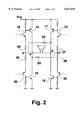
- FIG. 2 is a diagram showing a circuit according to another preferred embodiment of the present invention.
- FIG. 3 is a diagram showing prior art.
- first and second output transistors 15, 16 are SEPP (single ended push pull) connected, and the third and fourth output transistors 17, 18 are also SEPP connected.
- the first and second output transistors 15, 16 are driven by first and second driving transistors 19 and 20, respectively, which are connected at a point a and the connecting point a is connected to the connection point d of the third and fourth output transistors 17, 18.
- the third and fourth output transistors 17, 18 are driven by third and fourth driving transistors 21, 22, respectively, which are connected at a point c and the connecting point c is connected to the connection point b of the first and second output transistors 15, 16.
- a resistor 23 is connected between the connecting points a and d for limiting the current flowing between them.
- a resistor 24 is connected between the connecting points b and c for limiting the current flowing between them. Note that elements corresponding to those in FIG. 3 are given identical reference numerals.
- the amplifier 1 receives a negative input signal, the amplifier 1 outputs a signal, upon which the first input transistor 2 is turned off and the second input transistor 3 is turned on. Similar to the operation described with reference to FIG. 3, the first and fourth output transistors 15, 18 are then turned on.
- the connecting point a between the first and second driving transistors 19, 20 is connected to the connecting point d between the third and fourth output transistors 17, 18, the collector voltage thereof becomes closer to the earth level when the fourth output transistor 18 is turned on. Accordingly, the emitter voltage of the first driving transistor 19 also becomes closer to the earth level. With the emitter voltage of the first driving transistor 19 at the closer level to the earth level, the base voltage of the transistor 19 becomes higher than the value closer to the earth level by Vbe19 , Vbe19 being a base-emitter voltage of the first transistor 19. As a result, the voltage difference between the collector and the emitter of the first current source transistor 13 enlarges, so that the first current source transistor 13 becomes unlikely to be saturated.
- the connecting point c between the third and fourth driving transistors 21, 22 is connected to the connecting point b between the first and second output transistors 15, 16, the emitter voltage of the fourth transistor 22 becomes closer to the power source voltage Vcc when the first output transistor 15 is turned on. Therefore, providing that the base-emitter voltage of the fourth driving transistor 22 is Vbe22, the collector voltage of the second input transistor 3 becomes lower than the voltage closer to the power voltage Vcc by Vbe22. As a result, the voltage difference between the collector and the emitter of the second input transistor 3 enlarges, so that the second input transistor 13 becomes unlikely to be saturated.
- the collector voltage of the fourth output transistor 18 With a larger negative input signal applied to the amplifier 1, the collector voltage of the fourth output transistor 18 becomes much closer to the earth level, and that of the first output transistor 15 becomes much closer to the power voltage Vcc. This results in enlarging the voltage difference between the collector and emitter voltages of the first current source transistor 13 and that of the second input transistor 3. As a result, the first current source transistor 13 and the second input transistor 3 become unlikely to be saturated.
- the saturation voltage of the BTL amplifying circuit shown in FIG. 1 is determined according to the collector-emitter saturation voltages of the first and fourth output transistors 15 and 18.
- the amplifier 1 when a positive input signal is input to the input amplifier 1, the amplifier 1 outputs a signal, upon which the first input transistor 2 is turned on and the second input transistor 3 is turned off. Accordingly, the second and third output transistors 16 and 17 are turned on.
- the connecting point c between the third and fourth driving transistor 21 and 22 is connected to the connecting point b between the first and second output transistors 15 and 16, the collector voltage of the second output transistor 16 becomes closer to the earth level when the second output transistor 16 is turned on. Accordingly, the emitter voltage of the third driving transistor 21 also becomes closer to the earth level, upon which the base voltage thereof becomes higher than the value closer to the earth by Vbe21.
- Vbe21 is a base-emitter voltage of the third driving transistor 21. Therefore, a voltage difference between the collector and the emitter of the second current source transistor 14 enlarges.
- the connecting point a between the first and second driving transistor 19 and 20 is connected to the connecting point d between the third and fourth output transistors 17 and 18, the emitter voltage of the second driving transistor 20 becomes closer to the power voltage Vcc when the third output transistor 17 is turned on. Therefore, assuming that the base-emitter voltage of the second driving transistor 20 is as Vbe22, the collector voltage of the first input transistor 2 becomes lower than the voltage closer to the power voltage Vcc by Vbe20. As a result, a voltage difference between the collector and the emitter of the second input transistor 2 enlarges, so that the first input transistor 2 becomes unlikely to be saturated.
- the collector voltage of the second output transistor 16 With a larger positive input signal, the collector voltage of the second output transistor 16 becomes closer to the earth level, while the collector voltage of the third output transistor 17 becomes closer to the power source voltage Vcc. As a result, voltage differences between the collectors and the emitters of the second driving transistor 14 and the first input transistor 2 further enlarge, so that the second driving transistor 14 and the first input transistor 2 become further unlikely to be saturated.
- the saturation voltage of the BTL amplifying circuit shown in FIG. 1 is determined according only to the collector-emitter saturation voltages of the second and third output transistors 16 and 17.
- resistors 23 and 24 are connected for current limitation. With a negative input signal applied, the resistors 24 and 23 limit the current flowing from the connection point b to the connection point c and from the connection point a to the connection point d, respectively. With a positive input signal applied, on the contrary, they limit the current flowing from the connection point c to the connection point b and from the connection point a to the connection point a.
- connection points a-d and between b-c varies with the same phases. If these points are shorted without providing the resistors 23 and 24, the current flowing between these points will vary remarkably with the same phases. This may cause to increase a base current to be supplied to the output transistors, and thus a current flowing in the output transistors. This results in causing oscillation to the amplifying circuit of FIG. 1.
- the resistors 23, 24 are provided to limit the current flowing between respective connection points so that a steady current can be supplied to the output transistors. This can resultantly prevent oscillation.
- the resistances of the resistors 23, 24 are preferably set at a value which can at least prevent oscillation.
- resistors 25 and 26 are connected between the emitters of the first and second driving transistors 19 and 20 for controlling an idling current; and resistors 27 and 28 are connected between the emitters of the third and fourth transistors 21 and 22 for controlling an idling current.
- the connecting point a' between the resistors 23 and 24 is connected via a resistor 23 to the connecting point d, while connecting point c' between the resistors 27 and 28 is connected via the resistor 24 to the connecting point b.
- the emitter current of the first driving transistor 19 flows via the resistor 25 to the fourth output transistor 18.
- the base voltage of the first driving transistor 19 increases, and the current flowing the first and fourth output transistors 15, 18 thus also increases. This further causes to increase the emitter current of the first transistor 19.
- the base-emitter voltage of the first driving transistor 19 tends to increase.
- the voltage at the resistor 25 drops, and the emitter voltage of the first driving transistor 19 thus increases at a ratio substantially equal to that at which the base voltage thereof increases.
- the voltage difference between the base and the emitter of the first driving transistor 19 remains the same, and the emitter current thereof 19 will not increase.
- the collector current of the first output transistor 15 partly flows via the resistor 28 to the fourth driving transistor 22. Then, the base voltage of the fourth driving transistor 22 drops, and the emitter current thereof tends to increase. When a current to flow to the resistor 38 tends to increase, the voltage at the resistor 28 drops, and the emitter voltage of the fourth driving transistor 22 thereby drops. As a result, the voltage difference between the emitter and the base of the fourth driving transistor 22 remains the same, and the emitter current thereof will not increase.
- the base voltage of the third driving transistor 21 increases, and the emitter current thereof tends to increase.
- the voltage at the resistor 27 drops, and the emitter voltage of the third driving transistor 21 thereby increases.
- the voltage difference between the emitter and the base of the third driving transistor 21 remains the same, and the emitter current thereof will not increase.
- the emitter current thereof tends to increase.
- the voltage at the resistor 26 drops, and the emitter voltage of the second driving transistor 20 thereby drops.
- the voltage difference between the emitter and the base of the second driving transistor 20 remains the same, and the emitter current thereof will not increase.
- resistors 25 to 28 can prevent variation of the emitter current of the respective driving transistors. This enables to prevent variation of an idling current and to achieve additional advantage of preventing deterioration of a distortion ratio of an output signal from a BTL amplifying circuit.
Abstract
Description
Claims (3)
Applications Claiming Priority (2)
| Application Number | Priority Date | Filing Date | Title |
|---|---|---|---|
| JP30056397A JP3253573B2 (en) | 1997-10-31 | 1997-10-31 | BTL amplifier circuit |
| JP9-300563 | 1997-10-31 |
Publications (1)
| Publication Number | Publication Date |
|---|---|
| US6037839A true US6037839A (en) | 2000-03-14 |
Family
ID=17886347
Family Applications (1)
| Application Number | Title | Priority Date | Filing Date |
|---|---|---|---|
| US09/179,214 Expired - Lifetime US6037839A (en) | 1997-10-31 | 1998-10-27 | BTL amplifying circuit |
Country Status (5)
| Country | Link |
|---|---|
| US (1) | US6037839A (en) |
| EP (1) | EP0913930B1 (en) |
| JP (1) | JP3253573B2 (en) |
| KR (1) | KR100394301B1 (en) |
| DE (1) | DE69820836T2 (en) |
Cited By (1)
| Publication number | Priority date | Publication date | Assignee | Title |
|---|---|---|---|---|
| CN1300799C (en) * | 2002-04-02 | 2007-02-14 | 国际商业机器公司 | Sensing position of pin on tape inside cartridge shell |
Families Citing this family (2)
| Publication number | Priority date | Publication date | Assignee | Title |
|---|---|---|---|---|
| JP3881448B2 (en) * | 1998-03-31 | 2007-02-14 | 株式会社東芝 | Power amplifier circuit |
| KR101017733B1 (en) * | 2007-08-27 | 2011-02-28 | 산요 세미컨덕터 컴퍼니 리미티드 | Power amplifier for driving load |
Citations (3)
| Publication number | Priority date | Publication date | Assignee | Title |
|---|---|---|---|---|
| US4355287A (en) * | 1980-09-30 | 1982-10-19 | Rca Corporation | Bridge amplifiers employing complementary field-effect transistors |
| DE3436247A1 (en) * | 1984-10-03 | 1986-04-03 | Blaupunkt-Werke Gmbh, 3200 Hildesheim | Power amplifier |
| US4910477A (en) * | 1989-03-27 | 1990-03-20 | Elantec | Bridge-type linear amplifier with wide dynamic range and high efficiency |
Family Cites Families (2)
| Publication number | Priority date | Publication date | Assignee | Title |
|---|---|---|---|---|
| JPS57208711A (en) * | 1981-06-19 | 1982-12-21 | Hitachi Ltd | Power amplifier having one set inverted output |
| JP3505325B2 (en) * | 1996-09-20 | 2004-03-08 | 三洋電機株式会社 | BTL amplifier circuit |
-
1997
- 1997-10-31 JP JP30056397A patent/JP3253573B2/en not_active Expired - Fee Related
-
1998
- 1998-10-27 US US09/179,214 patent/US6037839A/en not_active Expired - Lifetime
- 1998-10-30 DE DE69820836T patent/DE69820836T2/en not_active Expired - Fee Related
- 1998-10-30 EP EP98308927A patent/EP0913930B1/en not_active Expired - Lifetime
- 1998-10-30 KR KR10-1998-0046348A patent/KR100394301B1/en not_active IP Right Cessation
Patent Citations (3)
| Publication number | Priority date | Publication date | Assignee | Title |
|---|---|---|---|---|
| US4355287A (en) * | 1980-09-30 | 1982-10-19 | Rca Corporation | Bridge amplifiers employing complementary field-effect transistors |
| DE3436247A1 (en) * | 1984-10-03 | 1986-04-03 | Blaupunkt-Werke Gmbh, 3200 Hildesheim | Power amplifier |
| US4910477A (en) * | 1989-03-27 | 1990-03-20 | Elantec | Bridge-type linear amplifier with wide dynamic range and high efficiency |
Cited By (1)
| Publication number | Priority date | Publication date | Assignee | Title |
|---|---|---|---|---|
| CN1300799C (en) * | 2002-04-02 | 2007-02-14 | 国际商业机器公司 | Sensing position of pin on tape inside cartridge shell |
Also Published As
| Publication number | Publication date |
|---|---|
| EP0913930A2 (en) | 1999-05-06 |
| JPH11136048A (en) | 1999-05-21 |
| EP0913930B1 (en) | 2004-01-02 |
| JP3253573B2 (en) | 2002-02-04 |
| EP0913930A3 (en) | 2002-03-20 |
| KR19990037538A (en) | 1999-05-25 |
| DE69820836D1 (en) | 2004-02-05 |
| KR100394301B1 (en) | 2003-09-19 |
| DE69820836T2 (en) | 2004-12-09 |
Similar Documents
| Publication | Publication Date | Title |
|---|---|---|
| US5442320A (en) | Mirror and bias circuit for class AB output stage with large swing and output drive | |
| US7113041B2 (en) | Operational amplifier | |
| US4254379A (en) | Push-pull amplifier circuit | |
| US4922208A (en) | Output stage for an operational amplifier | |
| US6037839A (en) | BTL amplifying circuit | |
| JPH05206751A (en) | Dynamic bias for class-a amplifier use | |
| US4165494A (en) | Bi-state linear amplifier | |
| US5343165A (en) | Amplifier having a symmetrical output characteristic | |
| JPH0369441B2 (en) | ||
| US5157347A (en) | Switching bridge amplifier | |
| US5376900A (en) | Push-pull output stage for amplifier in integrated circuit form | |
| US4803442A (en) | Low power buffer amplifier | |
| US4491804A (en) | Bias circuit which is independent of output device voltage characteristics for biasing an amplifier in class AB operation | |
| JP3505325B2 (en) | BTL amplifier circuit | |
| JPH0230902Y2 (en) | ||
| JP3349334B2 (en) | Differential amplifier | |
| JP2623954B2 (en) | Variable gain amplifier | |
| EP0028229B1 (en) | A balanced amplifier output stage | |
| JP3784910B2 (en) | Output circuit | |
| JPS6119547Y2 (en) | ||
| JP3172310B2 (en) | Buffer circuit | |
| JP2797504B2 (en) | Power amplifier circuit | |
| JP2604530Y2 (en) | Output circuit | |
| JPH0786843A (en) | Amplifier circuit | |
| JPH0786895A (en) | Output circuit |
Legal Events
| Date | Code | Title | Description |
|---|---|---|---|
| AS | Assignment |
Owner name: SANYO ELECTRIC CO., LTD., JAPAN Free format text: ASSIGNMENT OF ASSIGNORS INTEREST;ASSIGNORS:KOKUBO, KENICHI;TATANI, KOJI;TAIRA, TAKAYUKI;REEL/FRAME:009544/0778 Effective date: 19981022 |
|
| STCF | Information on status: patent grant |
Free format text: PATENTED CASE |
|
| FPAY | Fee payment |
Year of fee payment: 4 |
|
| CC | Certificate of correction | ||
| FPAY | Fee payment |
Year of fee payment: 8 |
|
| FEPP | Fee payment procedure |
Free format text: PAYOR NUMBER ASSIGNED (ORIGINAL EVENT CODE: ASPN); ENTITY STATUS OF PATENT OWNER: LARGE ENTITY |
|
| AS | Assignment |
Owner name: SEMICONDUCTOR COMPONENTS INDUSTRIES, LLC, ARIZONA Free format text: ASSIGNMENT OF ASSIGNORS INTEREST;ASSIGNOR:SANYO ELECTRIC CO., LTD.;REEL/FRAME:026594/0385 Effective date: 20110101 |
|
| FPAY | Fee payment |
Year of fee payment: 12 |
|
| AS | Assignment |
Owner name: SEMICONDUCTOR COMPONENTS INDUSTRIES, LLC, ARIZONA Free format text: CORRECTIVE ASSIGNMENT TO CORRECT THE INCORRECT #12/577882 PREVIOUSLY RECORDED ON REEL 026594 FRAME 0385. ASSIGNOR(S) HEREBY CONFIRMS THE ASSIGNMENT;ASSIGNOR:SANYO ELECTRIC CO., LTD;REEL/FRAME:032836/0342 Effective date: 20110101 |
|
| AS | Assignment |
Owner name: DEUTSCHE BANK AG NEW YORK BRANCH, NEW YORK Free format text: SECURITY INTEREST;ASSIGNOR:SEMICONDUCTOR COMPONENTS INDUSTRIES, LLC;REEL/FRAME:038620/0087 Effective date: 20160415 |
|
| AS | Assignment |
Owner name: DEUTSCHE BANK AG NEW YORK BRANCH, AS COLLATERAL AG Free format text: CORRECTIVE ASSIGNMENT TO CORRECT THE INCORRECT PATENT NUMBER 5859768 AND TO RECITE COLLATERAL AGENT ROLE OF RECEIVING PARTY IN THE SECURITY INTEREST PREVIOUSLY RECORDED ON REEL 038620 FRAME 0087. ASSIGNOR(S) HEREBY CONFIRMS THE SECURITY INTEREST;ASSIGNOR:SEMICONDUCTOR COMPONENTS INDUSTRIES, LLC;REEL/FRAME:039853/0001 Effective date: 20160415 Owner name: DEUTSCHE BANK AG NEW YORK BRANCH, AS COLLATERAL AGENT, NEW YORK Free format text: CORRECTIVE ASSIGNMENT TO CORRECT THE INCORRECT PATENT NUMBER 5859768 AND TO RECITE COLLATERAL AGENT ROLE OF RECEIVING PARTY IN THE SECURITY INTEREST PREVIOUSLY RECORDED ON REEL 038620 FRAME 0087. ASSIGNOR(S) HEREBY CONFIRMS THE SECURITY INTEREST;ASSIGNOR:SEMICONDUCTOR COMPONENTS INDUSTRIES, LLC;REEL/FRAME:039853/0001 Effective date: 20160415 |
|
| AS | Assignment |
Owner name: FAIRCHILD SEMICONDUCTOR CORPORATION, ARIZONA Free format text: RELEASE OF SECURITY INTEREST IN PATENTS RECORDED AT REEL 038620, FRAME 0087;ASSIGNOR:DEUTSCHE BANK AG NEW YORK BRANCH, AS COLLATERAL AGENT;REEL/FRAME:064070/0001 Effective date: 20230622 Owner name: SEMICONDUCTOR COMPONENTS INDUSTRIES, LLC, ARIZONA Free format text: RELEASE OF SECURITY INTEREST IN PATENTS RECORDED AT REEL 038620, FRAME 0087;ASSIGNOR:DEUTSCHE BANK AG NEW YORK BRANCH, AS COLLATERAL AGENT;REEL/FRAME:064070/0001 Effective date: 20230622 |