US5886909A - Defect diagnosis using simulation for IC yield improvement - Google Patents
Defect diagnosis using simulation for IC yield improvement Download PDFInfo
- Publication number
- US5886909A US5886909A US08/994,960 US99496097A US5886909A US 5886909 A US5886909 A US 5886909A US 99496097 A US99496097 A US 99496097A US 5886909 A US5886909 A US 5886909A
- Authority
- US
- United States
- Prior art keywords
- defect
- wafer
- defects
- method defined
- simulations
- Prior art date
- Legal status (The legal status is an assumption and is not a legal conclusion. Google has not performed a legal analysis and makes no representation as to the accuracy of the status listed.)
- Expired - Lifetime
Links
Images


Classifications
-
- H—ELECTRICITY
- H01—ELECTRIC ELEMENTS
- H01L—SEMICONDUCTOR DEVICES NOT COVERED BY CLASS H10
- H01L22/00—Testing or measuring during manufacture or treatment; Reliability measurements, i.e. testing of parts without further processing to modify the parts as such; Structural arrangements therefor
- H01L22/20—Sequence of activities consisting of a plurality of measurements, corrections, marking or sorting steps
Definitions
- This invention relates to the field of integrated circuit processing, and more particularly, to the detection and correction of defects that occur during wafer fabrication.
- Defects are major causes of yield loss for all integrated circuit ("IC") products.
- the focus of yield improvement efforts is to identify and eliminate major yield limiters. This is done, in part, by scanning a sample of IC wafers with in-line scanners and classifying defects. The most common defect types are identified, after which an effort is made to find the source of these common defects and fix the problem.
- Identifying a cause of a defect is usually the most time consuming and costly component of yield improvement efforts. Some defect types are not too difficult to diagnose. Easy to diagnose defects include those caused by particles. Such defects are often still present during in-line inspection. Consequently, the particle composition can be determined by known techniques, such as energy dispersion spectroscopy analysis.
- defect types are difficult to diagnose because they leave their imprint by distorting the physical topography of the water surface. These defects may also no longer be present at a step where inspection can be performed, which makes identification difficult. Examples of such defects can include bubbles and particles in the photoresist layer of the IC. As those skilled in the art will appreciate, diagnosis of defects in the photoresist layer is difficult because photoresist can only be inspected after it is developed. Moreover, bubble and particle defects in the photoresist often do not appear as bubbles or particles after the photoresist is developed, but may take on some other distorted shape or appearance, which further complicates diagnosis.
- yield learning typically involves running pre-designed experiments. Such experiments commonly involve processing sets of wafers with different fabrication recipes. Often, the number of wafers used in such experiments is limited, however, in order to save material costs. But if too few wafers are used, experimental results may turn out to be inconclusive thus frustrating defect diagnosis and yield improvement. Defect simulation can thus provide guidance for such experimental work by eliminating some of the competing theories about the causes of certain defects.
- lithography defect simulation has been known to provide insight about how defects of different sizes and types can distort expected wafer profiles.
- defect causes can be identified and verified by comparing the simulation results with observed wafer profiles.
- Both the insight and data gained from lithography simulation such as when and how defects cause shorts or opens, and the nature of the distorted patterns the defects cause, can assist in yield improvement efforts.
- Topography simulations of photoresist bubbles have been performed using the Metropole lithography simulator developed at Carnegie Mellon University. Among the capabilities of this simulator is a two-dimensional modeling of in-line aerial imaging, exposure of photoresist, and development of photoresist. The quantitative accuracy of the defect simulations was verified by simulating particles of various sizes in the photoresist. Experiments were then performed to recreate the photoresist defects in actual IC wafers. These experimental results were found to correlate and match those from the simulations.
- the simulator can be used to run further experiments to observe how a wide variety of defects are likely to impact photoresist profiles.
- the results from simulations of various defects such as the impact of bubbles and particles in the photoresist and on top of the photoresist layer, can then be employed to determine and correlate simulated defects with observed defects. This has been done for individual defects and for similar groupings of related defect types.
- What is needed is a method or technique for cataloging or storing a host of defect simulations that can then be used to diagnose the wide variety of defects encountered in a production environment.
- the catalog would include entries for known defects, and a profile of the simulated effect of such defect in IC processing. Observed defects could then be matched with the simulated defect effects. Once a match of simulated and observed effects is found, the associated cause of the defect can be readily identified.
- Such a catalog or library of defect profiles would help cut down the time required to identify the cause of a defect.
- known techniques can then be applied to correct the particular defect identified.
- the present invention provides a method for defect diagnosis using simulation for wafer yield improvement.
- a method is provided of diagnosing defects that impact topography of an integrated circuit wafer surface.
- An integrated circuit wafer surface is scanned after predetermined processing steps have been performed on the wafer, and any defect data detected from the scanned wafer is stored in a defect profile.
- the stored defect profile is compared against a library of wafer surface defect types based on known wafer defect characteristics to identify a possible cause for the defect profile.
- Predetermined experiments are run in order to narrow the number of feasible defect causes for the defect profile.
- the wafer surface defects can then be fixed according to known techniques based on the specific feasible defect causes identified.
- a method of developing a library of defects in integrated circuits is provided.
- a defect simulator is calibrated to match nominal wafer data for a non-defective integrated circuit.
- Plural defect simulations are executed to determine the effect of changes in size and composition of known defects.
- defect profiles of common defects and their characteristics are developed based on the defect simulations.
- These defect profiles are then stored in a library for later comparison of the defect profiles against actual wafer defects.
- potential defect profiles are classified as feasible or infeasible causes of the actual water defects based on the comparison.
- Predetermined experiments are then performed to narrow down the set of feasible causes for the actual defects.
- a method is provided of diagnosing defects in integrated circuits that impact doping concentrations.
- Integrated circuit wafer electrical test data is first measured, and a determination is made to see if at least one wafer site demonstrates bad wafer electrical test data.
- a simulator is then calibrated to match nominal wafer electrical test data.
- Plural defect simulations are performed, which can be used to compare simulated data with measured wafer electrical test data.
- the defect simulation results are classified as feasible or infeasible causes of the bad wafer electrical test data.
- Predetermined tests are performed to narrow the set of feasible causes of the bad wafer electrical test data by using different known test structures.
- the identified defect can then be fixed according to known techniques.
- the cataloging of a host of defect simulations can be used to diagnose a wide variety of defects encountered in an IC production environment.
- the catalog thus includes entries for known defects, and a profile of the simulated appearance of such defect in IC processing. Defects encountered during manufacturing can then be matched with the simulated defect appearances. Once a match of simulated and observed defect appearances is found, the associated cause of the defect is readily identified.
- the catalog of defect profiles can be stored in a computer memory to further automate the defect detection process. Such a library of defect profiles would help to cut down the time required to identify the cause of a defect, and thus the time and costs associated with IC yield improvement efforts. Once the defect type is identified, known techniques can then be applied to correct a particular defect.
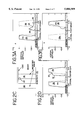
- FIG. 1 is a plan view of a semiconductor integrated circuit wafer after predetermined processing steps have been performed on the wafer.
- FIGS. 2A, 2B, 2C and 2D show a block cross-section and the simulation of a 0.2 ⁇ m bubble in the photoresist layer of the integrated circuit wafer shown in FIG. 1, where FIG. 2(A) shows a bubble located far from the substrate and close to the surface, and FIG. 2(C) shows a bubble close to unexposed areas of the photoresist layer.
- FIGS. 3A and 3B show further simulations of 0.2 ⁇ m bubbles in the photoresist layer, where the bubble shown in FIG. 3(A) is to the left of the bubble shown in FIG. 3(B), and both bubbles are between the bubbles shown in FIGS. 1 and 2.
- FIGS. 4A and 4B show another block cross-section and simulation of a 0.2 ⁇ m bubble in the photoresist layer where the bubble is located closer to the substrate.
- FIGS. 5A and 5B show a block cross-section and the simulation of a 0.1 ⁇ m tungsten particle in a 0.4 ⁇ m space between resist lines.
- FIG. 6 shows another simulation of a 0.1 ⁇ m nitride particle in a 0.4 ⁇ m space between resist lines.
- FIG. 7 shows block cross-sections and the simulations of 0.4 ⁇ m photoresist particles on the wafer surface in differing positions, where FIG. 7(A) shows the effect of a particle in position A, FIG. 7(B) shows the effect of a particle in position B, and FIG. 7(C) shows the effect of a particle in position C.
- FIGS. 8A and 8B show a block cross-section and simulations of 0.4 ⁇ m tungsten particle located on the wafer surface.
- FIGS. 9A and 9B are flow charts of the presently preferred method of the invention, where FIG. 9 (A) illustrates the flow of detecting a defect in wafer topography, and FIG. 9(B) illustrates the flow of detecting a defect in wafer doping concentrations.
- FIG. 1 a semiconductor integrated circuit wafer 10 is shown in FIG. 1.
- the wafer 10 in FIG. 1 is shown in plan view and displays a wafer 10 after predetermined processing steps have been performed on the wafer 10.
- the wafer 10 is examined and simulated after the photoresist layer has been deposited on the wafer surface.
- teachings of the invention can be applied after any number of processing steps have been performed on the wafer 10 depending on the nature of the defect observed and its relative location in the processing steps of the IC wafer 10.
- defects of various kinds are simulated and the simulations are stored for later comparison to observed defects.
- the simulation Prior to the storage of a simulated defect, however, the simulation is first compared against an experimentally created defect. This is done to verify that the simulation in fact accurately represents an actual defect. Once the simulation is confirmed, the profile of the simulated defect can be used for comparison to observed defects encountered during wafer production.
- the Metropole defect simulator developed by Carnegie-Mellon University, is employed to create the simulated defects.
- the propagation of light within the photoresist layer is described by Maxwell's equations, which are solved using a waveguide method so that systems with high numerical aperture ("NA") can be modeled accurately.
- the aerial imaging parameters are preferably set according to existing process recipes. In the presently preferred embodiment, an 5-layer metal, 0.35 micron, Complementary Metal Oxide Semiconductor process is used.
- the photoresist exposure parameters i.e. Dill's parameters, provided by the photoresist manufacturer, Shipley Co. of Marlboro, Mass., were entered into the simulator.
- the parameters that describe the development rate of the presently preferred I-Line photoresist are less exact, but have nevertheless been chosen according to the manufacturer's specifications.
- FIGS. 2-8 Examples of some of the defects detected in the preferred embodiment are shown in FIGS. 2-8.
- FIGS. 2-4 for example, the effects of 0.2 ⁇ m bubbles in the photoresist layer of the wafer 10 are considered. These bubbles can appear in the vicinity of lines 12 (FIG. 1) that are preferably 0.4 ⁇ m wide and preferably separated by 0.4 ⁇ m.
- the thickness of the photoresist (not shown) is also preferably slightly over 1 ⁇ m.
- FIGS. 2(A) and 2(B) are profiles which represent cross-sections of photoresist lines.
- the diagrams outline the physical boundary 14 between air and photoresist 28, the defect 22, and the substrate 20 after the photoresist 28 is developed.
- defects in the form of bubbles 22 located between unexposed areas of photoresist 28 are known to cause bridging 24 effects if located far from the substrate 26 and close to the photoresist surface 28.
- the bubble 22 in the photoresist 28 blocks the exposure of the photoresist 28 beneath the bubble 22. This occurs because of reflections off the bubble 22 itself.
- the simulation of this defect type shown in FIG. 2(A) tracks this known characteristic.
- a photoresist bubble 22 located close to unexposed areas of the photoresist 28 causes notching 30 and widening 32 of photoresist profiles below the bubble 20. Again, the widening of photoresist profiles results because the reflection of light off the bubble 22 blocks exposure of the photoresist 28 below it.
- the simulation shown in FIG. 2(B) accurately represents this type of defect profile.
- the resulting simulation of the defective photoresist profile caused by the appearance of bubbles 22 in the various locations of the photoresist 28 can be stored in a computer and compared with actual wafer profiles, as described in more detail below.
- FIG. 3 the impact of a bubble near the photoresist surface is simulated in various positions.
- the simulations shown in FIGS. 3(A) and 3(B) correspond to bubbles 22 that are located between those shown in FIGS. 2(A) and 2(B).
- the defect location in FIG. 3(A) results in an almost complete development 34 of one of the photoresist lines 28, except for some residual photoresist 36 directly under the bubble.
- Two-dimensional simulations of smaller bubbles in the same location indicate that the bubble results in a very deep notch 38 in the photoresist line 28, with some bridging to the adjacent photoresist line 28 near the sides of the notch 38 (FIG. 3(B)).
- the impact or effect of the bubble 22 is position dependent, and in the worst case such a bubble 22 can result in notching.
- the bubble 22 in FIG. 4 seems to cause a circular notch 44 in a photoresist line 28.
- the notch 44 is a result of reflection and scattering off of the defect towards the top of a nearby photoresist line 28. This scattering also results in a significant lowering of the PAC concentration at the top of the line, which consequently gets developed away 46.
- FIG. 5 a simulated profile resulting from a 0.1 ⁇ m particle 50 that is centered in the exposed space 52 between the two photoresist lines 28 is shown.
- these photoresist lines 28 are preferably 0.4 ⁇ m wide and preferably separated by 0.4 ⁇ m.
- the photoresist 28 under the particle 50 is not fully developed and bridging 54 thus occurs between photoresist lines 28.
- the simulation also shows in phantom lines the nominal appearance of the photoresist lines 28 without any defect.
- the resulting defect profile from these simulations can also be stored and later used for comparison with actual wafer profiles.
- the impact of particles 50 is also position dependent.
- the bridging 54 between lines 28 is more likely when the particle 50 is near the surface 14, and far from the substrate 20. If the particle 50 is not centered in the exposed area, bridging 54 is less likely.
- the composition of the particle 50 also affects the resulting photoresist profile.
- the simulation results shown in FIG. 5 represent tungsten and silicon particles 50, whose index of refraction differs significantly from that of the photoresist 28. If, on the other hand, the index of refraction of the material of the particle 50 is closer to that of photoresist 28, the effect is much less severe.
- 0.1 ⁇ m oxide particles 50 whose index of refraction is slightly below that of the photoresist 28, seem to have no impact on the photoresist profiles. If the index of refraction of the particle 50 is slightly above that of the photoresist 28, such as for nitride particles, only minor notching 56 of the photoresist profiles are observed. These effects can also be simulated (see FIG. 6).
- FIGS. 7(A)-(C) the position of a large 0.4 ⁇ m photoresist particle 70 is varied and the simulated effects are shown.
- the particle 70a is centered over an exposed area 72, it blocks the exposure (FIG. 7(A)).
- the particle 70c is centered over an unexposed area 74 (FIG.
- the exposed area under the particle 70 is not caused by reflections off the substrate 20, which are in turn reflected off the lower surface of the particle 70. Instead, light hitting the sides of the particle 70 is refracted and focused under the particle 70.
- Particles made of other materials with similar refractive properties to photoresist 28, like oxide and nitride, will result in similar photoresist patterns.
- the resulting photoresist profiles can also be used for comparison with actual wafer profiles, as described below.
- This defect pnenomenon is further illustrated by comparing simulation results of a tungsten particle with those of a photoresist particle.
- the tungsten particle results in widening of the photoresist line 28, but has no developed area under the particle 80 (see FIG. 8).
- FIG. 9(A) a flow chart 100 of the process of detecting defects that impact the topography of the wafer 10 surface is presented.
- in-line wafers are scanned and any defect data detected is stored for later comparison.
- the wafers are preferably scanned after predetermined process steps have been performed, as mentioned above.
- a pareto of nominal wafer topography data is developed and stored for later comparison.
- the most common defect types for the stored defect data are chosen. A process of elimination then begins where the chosen defect types are narrowed to identify the most likely cause of the observed defect.
- the elimination process begins by calibrating a simulator at step 108 to match wafer topography for the nominal case.
- the Metropole simulator is used.
- a plurality of defect simulations are executed by varying defect type, i.e., particle and bubble.
- Location (step 111a), size (step 111b) and composition (step 111c) of the defect are also varied as well.
- the simulated defect profiles are then compared at step 112 to the stored defect data. For each simulated defect profile, a comparison is made on whether it is a feasible or infeasible cause of the stored defective profile at step 114. Experiments are then performed at step 116 to narrow the range of feasible causes.
- a solution is identified for the most likely defect profile, and the defect is corrected according to this solution at step 120.
- a flow chart 200 of the process of detecting defects that impact doping concentrations is presented.
- the process begins at step 202 where wafer electrical test ("WET") data is reviewed. If a significant number of wafer sites have high resistance, and the distribution is non-uniform, then the failure analysis routine begins at step 204.
- WET wafer electrical test
- a simulator is calibrated to match nominal WET data. In the presently preferred embodiment, the Metropole simulator is used.
- Plural defect simulations are performed at step 208 by varying particle types and implant types. Varying the position (step 209a), size (step 209b) and composition (step 209c) of the defect are also simulated.
- the simulated electrical data are then compared at step 210 to the measured WET results.
- the simulated defect profiles are classified at step 212 as feasible or infeasible causes of the bad WET data. Tests are performed at step 214 to narrow down the range of feasible causes. Once a likely cause of the bad WET data is determined, a solution is identified at step 216, which is then implemented at step 218.
- the invention provides a less costly and time consuming method for identifying various defects caused during the manufacture of IC wafers.
- a defect simulation tool such as the Metropole simulator
- the impact of many different types of defects on photoresist profiles can be simulated and compared to in-line wafers.
- Defects such as bridging between photoresist lines caused by both very small bubbles and particles in the photoresist, as well as voids in the photoresist, caused by small bubbles or large particles on the photoresist surface, can be simulated and used for comparison to actual wafer defects.
- the automation of the process of detecting causes for observed wafer defects presents a useful advance over prior experimental techniques known in the art.
Abstract
Description
Claims (27)
Priority Applications (1)
| Application Number | Priority Date | Filing Date | Title |
|---|---|---|---|
| US08/994,960 US5886909A (en) | 1997-12-19 | 1997-12-19 | Defect diagnosis using simulation for IC yield improvement |
Applications Claiming Priority (1)
| Application Number | Priority Date | Filing Date | Title |
|---|---|---|---|
| US08/994,960 US5886909A (en) | 1997-12-19 | 1997-12-19 | Defect diagnosis using simulation for IC yield improvement |
Publications (1)
| Publication Number | Publication Date |
|---|---|
| US5886909A true US5886909A (en) | 1999-03-23 |
Family
ID=25541262
Family Applications (1)
| Application Number | Title | Priority Date | Filing Date |
|---|---|---|---|
| US08/994,960 Expired - Lifetime US5886909A (en) | 1997-12-19 | 1997-12-19 | Defect diagnosis using simulation for IC yield improvement |
Country Status (1)
| Country | Link |
|---|---|
| US (1) | US5886909A (en) |
Cited By (21)
| Publication number | Priority date | Publication date | Assignee | Title |
|---|---|---|---|---|
| US6136615A (en) * | 1999-10-29 | 2000-10-24 | Lucent Technologies, Inc. | Migration from control wafer to product wafer particle checks |
| US6327555B1 (en) * | 1998-04-28 | 2001-12-04 | Sony Corporation | Semiconductor simulation method |
| US20010054600A1 (en) * | 1999-03-31 | 2001-12-27 | Goldspring Gregory J. | Method and apparatus for simulating standard test wafers |
| US6349240B2 (en) * | 2000-03-27 | 2002-02-19 | Nec Corporation | Semiconductor device manufacturing system and method of manufacturing semiconductor devices |
| US6507933B1 (en) * | 1999-07-12 | 2003-01-14 | Advanced Micro Devices, Inc. | Automatic defect source classification |
| US20030023454A1 (en) * | 2001-06-25 | 2003-01-30 | Tokyo Electron Limited | Managing system, managing method, host computer, and information collecting/transmitting unit |
| US6556959B1 (en) * | 1999-07-12 | 2003-04-29 | Advanced Micro Devices, Inc. | Method and apparatus for updating a manufacturing model based upon fault data relating to processing of semiconductor wafers |
| US6583870B2 (en) * | 2000-05-30 | 2003-06-24 | Kabushiki Kaisha Toshiba | Simulated defective wafer and pattern defect inspection recipe preparing method |
| US6639663B1 (en) * | 2001-05-23 | 2003-10-28 | Advanced Micro Devices, Inc. | Method and apparatus for detecting processing faults using scatterometry measurements |
| US6694275B1 (en) * | 2000-06-02 | 2004-02-17 | Timbre Technologies, Inc. | Profiler business model |
| US6738954B1 (en) | 1999-12-08 | 2004-05-18 | International Business Machines Corporation | Method for prediction random defect yields of integrated circuits with accuracy and computation time controls |
| US6744266B2 (en) * | 2000-10-02 | 2004-06-01 | Applied Materials, Inc. | Defect knowledge library |
| US20040254752A1 (en) * | 2003-06-10 | 2004-12-16 | International Business Machines Corporation | System for identification of defects on circuits or other arrayed products |
| US6901340B1 (en) * | 2001-04-02 | 2005-05-31 | Advanced Micro Devices, Inc. | Method and apparatus for distinguishing between sources of process variation |
| US7106897B1 (en) | 2002-04-29 | 2006-09-12 | Advanced Micro Devices, Inc. | Universal spatial pattern recognition system |
| US20060230371A1 (en) * | 2005-04-06 | 2006-10-12 | Taiwan Semiconductor Manufacturing Co., Ltd. | Alternative methodology for defect simulation and system |
| US20080092095A1 (en) * | 2003-06-10 | 2008-04-17 | Mary Lanzerotti | Design Structure and System for Identification of Defects on Circuits or Other Arrayed Products |
| US20090119045A1 (en) * | 2007-11-02 | 2009-05-07 | United Microelectronics Corp. | Method of inspecting photomask defect |
| US7599051B1 (en) * | 2006-11-21 | 2009-10-06 | Kla-Tencor Technologies Corporation | Calibration of a substrate inspection tool |
| US20120046778A1 (en) * | 2010-08-20 | 2012-02-23 | Yoshiyuki Shioyama | Defect analyzing method and defect analyzing apparatus |
| CN107784660A (en) * | 2017-11-02 | 2018-03-09 | 武汉新芯集成电路制造有限公司 | Image processing method, image processing system and defect detecting device |
Citations (3)
| Publication number | Priority date | Publication date | Assignee | Title |
|---|---|---|---|---|
| US5585210A (en) * | 1993-04-22 | 1996-12-17 | Samsung Electronics Co., Ltd. | Mask pattern of a semiconductor device and a method of manufacturing fine patterns using the same |
| US5586039A (en) * | 1993-03-29 | 1996-12-17 | Texas Instruments Incorporated | Computer-aided manufacturing support method and system for specifying relationships and dependencies between process type components |
| US5808735A (en) * | 1993-06-17 | 1998-09-15 | Ultrapointe Corporation | Method for characterizing defects on semiconductor wafers |
-
1997
- 1997-12-19 US US08/994,960 patent/US5886909A/en not_active Expired - Lifetime
Patent Citations (3)
| Publication number | Priority date | Publication date | Assignee | Title |
|---|---|---|---|---|
| US5586039A (en) * | 1993-03-29 | 1996-12-17 | Texas Instruments Incorporated | Computer-aided manufacturing support method and system for specifying relationships and dependencies between process type components |
| US5585210A (en) * | 1993-04-22 | 1996-12-17 | Samsung Electronics Co., Ltd. | Mask pattern of a semiconductor device and a method of manufacturing fine patterns using the same |
| US5808735A (en) * | 1993-06-17 | 1998-09-15 | Ultrapointe Corporation | Method for characterizing defects on semiconductor wafers |
Non-Patent Citations (3)
| Title |
|---|
| Article Entitled, Photoresist Defect Diagnosis Using a Rigorous Topography Simulator, Author: Milor et al. * |
| Article Entitled, Photoresist Process Optimization For Defects Using A Rigorous Lithography Simulator, Author: Milor et al. * |
| Article Entitled, The Application Of Lithography Defect Simulation To Submicron CMOS Yield Improvement Efforts, Author: Milor et al. * |
Cited By (32)
| Publication number | Priority date | Publication date | Assignee | Title |
|---|---|---|---|---|
| US6327555B1 (en) * | 1998-04-28 | 2001-12-04 | Sony Corporation | Semiconductor simulation method |
| US20010054600A1 (en) * | 1999-03-31 | 2001-12-27 | Goldspring Gregory J. | Method and apparatus for simulating standard test wafers |
| US6507933B1 (en) * | 1999-07-12 | 2003-01-14 | Advanced Micro Devices, Inc. | Automatic defect source classification |
| US6556959B1 (en) * | 1999-07-12 | 2003-04-29 | Advanced Micro Devices, Inc. | Method and apparatus for updating a manufacturing model based upon fault data relating to processing of semiconductor wafers |
| US6136615A (en) * | 1999-10-29 | 2000-10-24 | Lucent Technologies, Inc. | Migration from control wafer to product wafer particle checks |
| US6738954B1 (en) | 1999-12-08 | 2004-05-18 | International Business Machines Corporation | Method for prediction random defect yields of integrated circuits with accuracy and computation time controls |
| US6349240B2 (en) * | 2000-03-27 | 2002-02-19 | Nec Corporation | Semiconductor device manufacturing system and method of manufacturing semiconductor devices |
| US20020059012A1 (en) * | 2000-03-27 | 2002-05-16 | Nec Corporation | Method of manufacturing semiconductor devices |
| US7054705B2 (en) | 2000-03-27 | 2006-05-30 | Nec Electronics Corporation | Method of manufacturing semiconductor devices |
| US6583870B2 (en) * | 2000-05-30 | 2003-06-24 | Kabushiki Kaisha Toshiba | Simulated defective wafer and pattern defect inspection recipe preparing method |
| CN100353514C (en) * | 2000-05-30 | 2007-12-05 | 株式会社东芝 | Method for stimulating defect chip and defect testing |
| US6694275B1 (en) * | 2000-06-02 | 2004-02-17 | Timbre Technologies, Inc. | Profiler business model |
| US6744266B2 (en) * | 2000-10-02 | 2004-06-01 | Applied Materials, Inc. | Defect knowledge library |
| US6901340B1 (en) * | 2001-04-02 | 2005-05-31 | Advanced Micro Devices, Inc. | Method and apparatus for distinguishing between sources of process variation |
| US6639663B1 (en) * | 2001-05-23 | 2003-10-28 | Advanced Micro Devices, Inc. | Method and apparatus for detecting processing faults using scatterometry measurements |
| US6766209B2 (en) * | 2001-06-25 | 2004-07-20 | Tokyo Electron Limited | Managing system, managing method, host computer, and information collecting/transmitting unit |
| US20030023454A1 (en) * | 2001-06-25 | 2003-01-30 | Tokyo Electron Limited | Managing system, managing method, host computer, and information collecting/transmitting unit |
| US7106897B1 (en) | 2002-04-29 | 2006-09-12 | Advanced Micro Devices, Inc. | Universal spatial pattern recognition system |
| US20080092095A1 (en) * | 2003-06-10 | 2008-04-17 | Mary Lanzerotti | Design Structure and System for Identification of Defects on Circuits or Other Arrayed Products |
| US7752581B2 (en) | 2003-06-10 | 2010-07-06 | International Business Machines Corporation | Design structure and system for identification of defects on circuits or other arrayed products |
| US20060265185A1 (en) * | 2003-06-10 | 2006-11-23 | International Business Machines Corporation | System for identification of defects on circuits or other arrayed products |
| US7346470B2 (en) | 2003-06-10 | 2008-03-18 | International Business Machines Corporation | System for identification of defects on circuits or other arrayed products |
| US20040254752A1 (en) * | 2003-06-10 | 2004-12-16 | International Business Machines Corporation | System for identification of defects on circuits or other arrayed products |
| US7356787B2 (en) * | 2005-04-06 | 2008-04-08 | Taiwan Semiconductor Manufacturing Co., Ltd. | Alternative methodology for defect simulation and system |
| CN100444178C (en) * | 2005-04-06 | 2008-12-17 | 台湾积体电路制造股份有限公司 | Defect simulation and system and method |
| US20060230371A1 (en) * | 2005-04-06 | 2006-10-12 | Taiwan Semiconductor Manufacturing Co., Ltd. | Alternative methodology for defect simulation and system |
| US7599051B1 (en) * | 2006-11-21 | 2009-10-06 | Kla-Tencor Technologies Corporation | Calibration of a substrate inspection tool |
| US20090119045A1 (en) * | 2007-11-02 | 2009-05-07 | United Microelectronics Corp. | Method of inspecting photomask defect |
| US7664614B2 (en) * | 2007-11-02 | 2010-02-16 | United Microelectronics Corp. | Method of inspecting photomask defect |
| US20120046778A1 (en) * | 2010-08-20 | 2012-02-23 | Yoshiyuki Shioyama | Defect analyzing method and defect analyzing apparatus |
| US8965551B2 (en) * | 2010-08-20 | 2015-02-24 | Kabushiki Kaisha Toshiba | Defect analyzing method and defect analyzing apparatus |
| CN107784660A (en) * | 2017-11-02 | 2018-03-09 | 武汉新芯集成电路制造有限公司 | Image processing method, image processing system and defect detecting device |
Similar Documents
| Publication | Publication Date | Title |
|---|---|---|
| US5886909A (en) | Defect diagnosis using simulation for IC yield improvement | |
| US11348222B2 (en) | Methods and systems for inspection of wafers and reticles using designer intent data | |
| US6721695B1 (en) | Method and apparatus for evaluating the runability of a photomask inspection tool | |
| US6784446B1 (en) | Reticle defect printability verification by resist latent image comparison | |
| US7853920B2 (en) | Method for detecting, sampling, analyzing, and correcting marginal patterns in integrated circuit manufacturing | |
| US8194968B2 (en) | Methods and systems for using electrical information for a device being fabricated on a wafer to perform one or more defect-related functions | |
| KR101056142B1 (en) | Computerized method for detecting defects in reticle design data | |
| US6539272B1 (en) | Electric device inspection method and electric device inspection system | |
| TWI767907B (en) | Computer assisted weak pattern detection and quantification system | |
| US7855088B2 (en) | Method for manufacturing integrated circuits by guardbanding die regions | |
| KR100755049B1 (en) | Analysis method of defect on photo mask | |
| KR20100034611A (en) | Method for verification of process window in semiconductor device | |
| KR970011652B1 (en) | Test method of lithography process margin of semiconductor | |
| Askary et al. | Redefining critical in critical dimension metrology | |
| CN117981066A (en) | System and method for weighting defects with co-located modeled flaws | |
| Milor et al. | Photoresist defect diagnosis using a rigorous topography simulator | |
| Reynolds | Assessing polylayer performance of UV defect detection systems |
Legal Events
| Date | Code | Title | Description |
|---|---|---|---|
| AS | Assignment |
Owner name: ADVANCED MICRO DEVICES, INC., CALIFORNIA Free format text: ASSIGNMENT OF ASSIGNORS INTEREST;ASSIGNORS:MILOR, LINDA;PENG, YENG-KAUNG;PHAN, KHOI ANH;AND OTHERS;REEL/FRAME:008940/0883 Effective date: 19971216 |
|
| STCF | Information on status: patent grant |
Free format text: PATENTED CASE |
|
| FPAY | Fee payment |
Year of fee payment: 4 |
|
| FPAY | Fee payment |
Year of fee payment: 8 |
|
| AS | Assignment |
Owner name: GLOBALFOUNDRIES INC., CAYMAN ISLANDS Free format text: AFFIRMATION OF PATENT ASSIGNMENT;ASSIGNOR:ADVANCED MICRO DEVICES, INC.;REEL/FRAME:023119/0083 Effective date: 20090630 |
|
| FPAY | Fee payment |
Year of fee payment: 12 |
|
| AS | Assignment |
Owner name: GLOBALFOUNDRIES U.S. INC., NEW YORK Free format text: RELEASE BY SECURED PARTY;ASSIGNOR:WILMINGTON TRUST, NATIONAL ASSOCIATION;REEL/FRAME:056987/0001 Effective date: 20201117 |