US5809536A - Method for reducing the number of coherency cycles within a directory-based cache coherency memory system uitilizing a memory state cache - Google Patents
Method for reducing the number of coherency cycles within a directory-based cache coherency memory system uitilizing a memory state cache Download PDFInfo
- Publication number
- US5809536A US5809536A US08/763,703 US76370396A US5809536A US 5809536 A US5809536 A US 5809536A US 76370396 A US76370396 A US 76370396A US 5809536 A US5809536 A US 5809536A
- Authority
- US
- United States
- Prior art keywords
- memory
- state
- line
- cache
- shared
- Prior art date
- Legal status (The legal status is an assumption and is not a legal conclusion. Google has not performed a legal analysis and makes no representation as to the accuracy of the status listed.)
- Expired - Lifetime
Links
Images


Classifications
-
- G—PHYSICS
- G06—COMPUTING; CALCULATING OR COUNTING
- G06F—ELECTRIC DIGITAL DATA PROCESSING
- G06F12/00—Accessing, addressing or allocating within memory systems or architectures
- G06F12/02—Addressing or allocation; Relocation
- G06F12/08—Addressing or allocation; Relocation in hierarchically structured memory systems, e.g. virtual memory systems
- G06F12/0802—Addressing of a memory level in which the access to the desired data or data block requires associative addressing means, e.g. caches
- G06F12/0806—Multiuser, multiprocessor or multiprocessing cache systems
- G06F12/0815—Cache consistency protocols
- G06F12/0817—Cache consistency protocols using directory methods
- G06F12/082—Associative directories
Definitions
- the present invention relates to multiprocessor computer systems having multiple data cache memories and a shared memory and, more particularly, to multiprocessor computer systems employing directory-based protocols for maintaining cache coherency.
- System and cache memories used primarily for the temporary storage of data, application software and operating system software, are also being utilized within more sophisticated multiprocessor systems for the storage of parity bits, cache coherency state information, and error detection and/or correction syndrome bits.
- an improved method for performing state cache line replacement operations in a multiprocessor computer system including plurality if data cache memories, a shared system memory, a state cache memory, and employing a centralized/distributed directory-based cache coherency system for maintaining consistency between lines of memory within the shared system memory and the plurality of data cache memories.
- a multiprocessor computer system is described in U.S. patent application Ser. No. 08/762,636, filed concurrently with the present application.
- U.S. patent application Ser. No. 08/762,636 entitled “Method and Apparatus for Caching State Information Within a Directory-Based Coherency Memory System," by Gene F. Young, Roy Stevens, and Larry James, is assigned to NCR Corporation.
- Each data cache memory contains a data cache memory line state with each line of memory saved within the data cache memory, the data cache memory line state being any one of the MESI (Modified-Exclusive-Shared-Invalid) states: MODIFIED, EXCLUSIVE, SHARED, or INVALID.
- the state cache memory contains a system memory line state for a predetermined number of lines of memory saved within the system memory, the system memory line state being any one of the following states: SHARED BUS A, SHARED BUS B, SHARED BOTH, OWNED BUS A and OWNED BUS B.
- the method for performing state cache line replacement operations includes the following steps: establishing a default system memory line state of SHARED for lines of memory represented in said state cache memory; reading the system memory line state for a previously stored state cache entry prior to a replacement of said previously stored state cache entry, said previously stored state cache entry being associated with a line of memory stored in said shared memory and at least one data cache memory; and performing a castout operation to update the line of memory within said shared memory and assigning a data cache memory line state of SHARED to said line of memory in each data cache memory containing said line of memory if said system memory line state for said previously stored state cache entry is OWNED (OWNED BUS A or OWNED BUS B).
- the described method reduces the number of coherency operations caused as a result of replacements in the state cache memory. Since most lines of memory are in a shared state, setting the default state to a shared state, rather than a uncached state, reduces the number of invalidate coherency operations which must be performed during state cache line replacements.
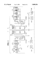
- FIG. 1 is a simple block diagram representation of an eight-processor super high volume (SHV) symmetric multiprocessing (SMP) computer system employing currently available commodity components.
- SHV super high volume
- SMP symmetric multiprocessing
- FIG. 2 is a block diagram representation of system memory 105A and a cache memory for the storage of state information.
- FIG. 3 is a block diagram representation of state cache memory 203 of FIG. 2 providing more detail concerning the structure and operation of state cache 203.
- FIG. 4 is a table illustrating reductions in replacement memory line coherency operations for three possible default memory line states in accordance with the present invention.
- FIGS. 5A and 5B provide a coherency state table for a three bit directory based memory having an "Uncached" default state in accordance with a traditional replacement procedure.
- FIGS. 6A and 6B provide a coherency state table for a three bit directory based memory having a "Shared Both" default state in accordance with a first embodiment of the present invention.
- FIGS. 7A and 7B provide a coherency state table for a three bit directory based memory having a "Shared Agent A" default state in accordance with a second embodiment of the present invention.
- NCR Corporation has developed an advanced multiprocessor architecture utilizing system techniques pioneered by NCR while also advantageously making use of standard high volume (SHV) components, such as Intel Pentium Pro processors, PCI I/O chipsets, Pentium Pro chipsets, Pentium Pro bus topology (P6), and standard memory modules (SIMMs and DIMMs).
- SHV high volume
- Intel Pentium Pro processors PCI I/O chipsets
- Pentium Pro chipsets Pentium Pro bus topology
- SIMMs and DIMMs standard memory modules
- FIG. 1 there is seen an eight-processor SMP system formed of two four-processor building blocks or complexes, identified by reference numerals A and B. Each complex is seen to include identical structure and components, which are identified by reference numerals ending in either an A or a B, for complex "A" and "B", respectively.
- the portion of the system contained in complex A is seen to include up to four processors 101A connected to a high-bandwidth split-transaction processor bus 103A. Associated with each processor 301A is a cache memory 321A.
- a system memory 105A is connected to bus 103A through an advanced dual-ported memory controller 107A.
- the processor bus 103A is connected to the first port of memory controller 107A.
- the second memory controller port connects to a high bandwidth I/O bus 115, also referred to herein as an expansion bus, which provides connection for multiple PCI I/O interfaces 109A. All of these components, with the exception of advanced memory controller 107A, are currently available commodity components.
- processors 101A may be Intel Pentium Pro processors and busses 103A and 115 may be Pentium Pro (P6) bus topology.
- the advanced memory controller (AMC) 107A manages control and data flow in all directions between processor bus 103A and I/O bus 115.
- the I/O bus may contain P6 to PCI I/O Bridges and another AMC ASIC for connectivity to another processor bus, as will be discussed below.
- the AMC 107A also controls access to a coherent DRAM memory array.
- the AMC as presently implemented consists of a control and data slice ASIC pair.
- complex B has a construction identical to complex A.
- the two complexes are interconnected by expansion bus 115, allowing for communication between the processors 101A and 101B, system memories 105A and 105B, as well as shared I/O devices, cache memories, and other components.
- Bus snooping is a method of keeping track of data movements between processors and memory. There are performance advantages to this system with a small number of tightly-coupled processors. If a processor needs data that is available in the data cache of another processor on the same bus, the data can be shared by both processors. Otherwise, the data must be retrieved from main memory 105A or 105B, a more time consuming operation which requires system bus traffic. This method enhances system performance by reducing system bus contention.
- the characteristics of the NCR architecture shown in FIG. 1 include:
- Dual ported memory controllers 107A and 107B permit connection and utilization of dual buses, each operating at 66 MHz with a bandwidth of 64 bits and capable of sustained data transfer rates of 533 MB/s.
- Dual bus approach provides greater scalability through a reduction of bus loadings and provision of a private processor to memory path that can operate independent of IOB to IOB traffic.
- Additional processors and I/O devices can be connected to the expansion bus 115.
- the system as described is able to fill High Availability Transaction Processing (HATP) and Scaleable Data Warehouse (SDW) server needs, while capitalizing on the computer industry's SHV motion.
- HATP High Availability Transaction Processing
- SDW Scaleable Data Warehouse
- data from a given memory location can reside simultaneously in main memory and in one or more data cache memories.
- data in main memory and in data cache memory may not always be the same. This may occur when a microprocessor updates the data contained in its associated data cache memory without updating the main memory and other data cache memories, or when another bus master changes data in main memory without updating its copy in the microprocessor data cache memories.
- system memory modules 105A and 105B To track the data moving between the processors, system memory modules 105A and 105B, and the various data cache memories, the system utilizes a hybrid of memory and cache based coherency. Coherency between system memory and caching agents, i.e., system bus processors with first and possibly second level data caches, is maintained via a combination centralized/distributed directory-based cache coherency.
- a directory-based cache coherency scheme is a method of keeping track of data movements between the processors and memory.
- a memory status table identifies which processors have which lines of memory in their associated data cache memories.
- the status table identifies the location within main memory or processor data cache where the most current copy of the data resides.
- the advantage of this method is that no additional work must be performed until a processor needs data that resides in a data cache that cannot be accessed through snooping.
- Directory-based cache coherency is most effective with a large number of tightly-coupled processors on a system bus.
- the centralized/distributed directory-based cache coherency scheme employed in the system shown in FIG. 1 consists of two directory elements.
- the central element within the directory scheme resides in state cache memories 203A and 203B associated with system memory modules 105A and 105B, respectively. This element is referred to as the Memory Line Status Table (MLST).
- MLST Memory Line Status Table
- Each active (cached) memory line within system memory includes a corresponding entry in the MLST. This corresponding entry contains information indicating whether or not a memory line is cached, and if so, whether it is exclusively owned by one processor (or bus), or shared across multiple processors (or buses).
- the directory scheme and MLST can be set up to identify memory line ownership by system bus or by processor.
- bit-per-bus distinguishes ownership on a bus basis
- more granular "bit-per-processor” MLST distinguishes ownership on a processor basis. Note that the distinction is specific to a memory design and hence transparent to any other device on the system bus.
- Distributed directory elements reside locally within each processor's data cache directory.
- the element associated with a particular processor is referred to as its Processor Line Status Table (PLST).
- PLST Processor Line Status Table
- Each cache line has a corresponding entry in the PLST. From the local processor's perspective, this entry contains information indicating whether or not a line contains a valid copy of a main memory line, and if so, whether or not modifications to that line must be broadcast to the rest of the system.
- each processor's PLST is a slave to special system bus cycles known as Memory Intervention Commands (MICs). These cycles query the PLST as to the local state of a particular line, and/or tell the PLST to change that local state.
- MICs Memory Intervention Commands
- the Modified-Exclusive-Shared-Invalid (MESI) cache coherency protocol is a hardware-implemented protocol for maintaining data consistency between main memory and data cache memories.
- a typical implementation of the MESI hardware cache coherency protocol requires the utilization of cache controllers having the ability to:
- MESI represents four states which define whether a line is valid, if it is available in other caches, and if it has been modified.
- Each line of data in a data cache includes an associated field which indicates whether the line of data is MODIFIED, EXCLUSIVE, SHARED, or INVALID.
- Each cache line is marked in one of the four possible MESI states:
- EXCLUSIVE (PE)--This state indicates a line of data which is exclusively available in only this cache, that this line is not Modified (main memory also has a valid copy), and that the local processor has the freedom to modify this line without informing the system.
- Exclusive data can not be used by any other processor until it is acted upon in some manner. Writing to an Exclusive line causes it to change to the Modified state and can be done without informing other caches, so no memory bus activity is generated. Note that lines in the (PE) state will be marked (MO) in the MLST, as will be described below.
- SHARED (PS)--This state indicates a line of data which is potentially shared with other caches (the same line may exist in one or more caches). Shared data may be shared among multiple processors and stored in multiple caches. A Shared line can be read by the local processor without a main memory access.
- INVALID (PI)--This state indicates a line of data is not available in the cache. Invalid data in a particular cache is not to be used for future processing, except diagnostic or similar uses. A read to this line will be a "miss” (not available). A write to this line will cause a write-through cycle to the memory bus. All cache lines are reset to the (PI) state upon system initialization.
- any writes to the owned line of memory within main memory will result in an immediate update of the same data contained within the processor's data cache memory.
- the Memory Line Status Table marks a memory line in one of three possible states: NOT CACHED (MNC), SHARED (MS), and OWNED (MO).
- MNC NOT CACHED
- MS SHARED
- MO OWNED
- the letter M distinguishes these states from PLST states, which are identified by use of the letter P. Additionally there are bus and/or processor state bits indicating sharing or ownership on either a bus or processor basis.
- MNC Indicates that no cache has a copy of that line. All memory lines must be reset to the (MNC) state upon system initialization.
- SHARED STATE Indicates that one or more caches potentially have a copy of that line.
- OWNED STATE Indicates that one and only one cache potentially has a copy of that line, and that the data in memory potentially does not match it (Memory data is referred to as stale).
- the MLST does not have the most up-to-date information about a particular memory line. For example, the MLST may mark a line as shared by two particular processors since it saw them both read it. However, both processors may have long since discarded that line to make room for new data without informing the MLST (referred to as "silent replacement"). The MLST will naturally "catch up” to the latest state of a particular line whenever an access to that line by some master forces a MIC.
- a write by a third processor to this line will initiate a (now superfluous) MIC to invalidate other cached copies, and will bring the MLST up-to-date.
- the MLST always holds a conservative view of the state of cache lines. That is, a line that is owned or shared by a processor will always be marked correctly in the MLST. "Stale" information in the MLST takes the form of lines marked owned or shared that are no longer present in any processor's data cache.
- MBI INVALIDATE
- MCOI CASTOUT INVALIDATE This cycle is initiated to cause a cache with a potentially modified copy of an addressed line to cast it out to system memory and to go to the invalid state (PI). It occurs in response to certain memory operations that access a memory line marked owned (MO) in the MLST. If the owning cache has the line in the modified (PM) state, it supplies the data and goes invalid. If the owning cache has the line in the exclusive (PE) state, it acknowledges the MBCOI and goes invalid, but does not supply the data. If the owning cache no longer has the line it simply acknowledges the MBCOI to complete the cycle.
- MO memory line marked owned
- PE exclusive
- MBCOS CASTOUT SHARED
- the MLST includes additional bus and/or processor state bits indicating sharing or ownership on either a bus or processor basis.
- the Bit-per-Bus Protocol uses three memory state bits per line to indicate the current state of the line. One bit indicates shared or owned, and the other two depict which bus (A or B) or buses (A and B) have the line shared or owned. Bus ownership indicates that one of the processors on that bus owns the line. Six states are possible: UNCACHED, SHARED BUS A, SHARED BUS B, SHARED BOTH, OWNED BUS A and OWNED BUS B. Note that a line can be owned by only one processor and therefore by only one bus. A shared line can be shared by one or more processors on each bus.
- the Bit-per-Processor Protocol has an MLST consisting of n+1 bits per line (n is equal to the number of processors) to indicate the current state of that line. One bit indicates whether the line is shared (MS) or owned (MO), and the other n bits depict which processor or processors have the line cached.
- a shared line can be shared by one or more processors on either or both buses.
- state cache memories 203A and 203B are sized to store state information for only a portion of the memory lines included in system memory in recognition that rarely will all of system memory be utilized (cached) at any one time.
- the structure and operation of an exemplary state cache memory 203A is illustrated in FIGS. 2 and 3.
- FIG. 2 shows system memory 105A having a size, for example, of one gigabyte (2 29 bytes) divided into 33,554,432 (2 25 ) million memory blocks or lines, each line having a size of 32 bytes.
- Data stored within memory 105A is accessed by submitting a 29-bit address 201.
- the 25 most significant bits within the address identified as "X" bits, identify the memory block or line number.
- the next 4 address bits, identified as "W” bits point to the word within the memory block, while the least significant address bit "B" identifies the byte within a word.
- the cache memory 203A providing for the storage of state information includes two sections identified as the "cache tag RAM” 205A and the “cache data RAM” 207A. Each line entry within state cache memory 203A contains state information saved to the cache data RAM and a four bit tag stored within the cache tag RAM.
- State cache memory 203A is indexed by a subset of the total number of memory address bits.
- the remainder of the address bits, or tag bits, are part of the contents for each entry in the storage device.
- the index bits define the number of entries in the state cache, and the tag bits determine the number of memory lines which can contend for the same entry in the state cache.
- the index bits plus the tag bits define the total number of memory lines which can be supported.
- the reduction in state storage is defined by the number of tag bits. For example, if the number of tag bits is four, then the state storage requirements for this concept are one sixteenth that of the traditional architecture.
- FIG. 3 More detailed information concerning the structure and operation of the state cache 203A is shown in FIG. 3. Entries within the state cache are accessed by submitting the same address 201 used to access main memory 105A. The four most significant bits within the address are identified as tag bits, and the next 21 address bits are identified as index bits. These 25 address bits are the same bits identified as X bits in FIG. 4, and which are used to identify memory blocks within main memory 105A.
- the index field of the address is used to specify the particular entry or line of cache to be checked.
- the tag bits of the address are compared with the tag of the selected cache line. If there is a match, a cache hit occurs and the state bits associated with the selected cache line are retrieved.
- the index field of an address is used to identify a particular entry or line of cache for tag and state information storage.
- the first four address bits are saved to the cache tag RAM while the state information associated with the address are saved to the cache data RAM.
- error detection and/or correction syndrome bits or parity bits could be included in the state cache memory.
- the state cache as described, is a direct mapped cache. Note, however, that the state cache can be associative, sectored, or direct mapped as with data caches.
- the operation of the memory system is as follows: When a read or write operation is requested of the system memory, the state cache is accessed to determine the coherency cycles necessary, dependent on the protocol. If the tag information in the state cache match the corresponding bits of the memory address, then the corresponding coherency cycles are performed and the state updated. If there is not a tag match, then coherency operations for the default state are performed (possibly none), and the new line address and state are allocated to the state cache. Possibly an existing entry will be replaced by the new line. Coherency operations may be required to bring the replaced line state to the default state. These replacement coherency operations are the performance cost for reducing the amount of state storage, but as mentioned above are negligible for a reasonable state cache size and typical workload. Note that the state cache can be associative, sectored, or direct mapped as with data caches.
- state cache memory The memory space saving provided though use of a state cache memory is illustrated in the following example.
- the basic coherency block or line of memory is 32 bytes.
- To store the 4 bit state for all of memory would require 16 MB of state memory (32 million lines times 4 bits per line).
- state memory If each entry in the state memory contains a 4 bit tag, the state memory would contain 8 bits of information per line which is double the traditional amount. However, only one sixteenth as many lines are needed due to the 4 bit tag. Therefore, the total state memory required is 2 MB which is only one eighth of the traditional amount.
- the tradeoff is possible replacements of the state cache entries which are relatively few. In this example, the state cache is equivalent to a 64 MB data cache (2 million entries, each representing 32 byte lines).
- the present invention provides a method for reducing the number of coherency operations caused as a result of replacements in a directory based memory state cache.
- FIG. 4 provides a table showing the replaced line operations for the traditional algorithm and the claimed method with a "Shared Both" or a "Shared Only" default state. Note a shared agent A or shared agent B default has merit if one agent has faster or higher priority access to memory; thus invalidates would be quicker for allocates to the state cache.
- FIGS. 5A and 5B show the coherency state table for a three-bit directory based memory with an uncached default state.
- the tables shown in FIGS. 6A-6B and 7A-7B show the coherency states for "Shared Both" and "Shared Agent A” default states. The states which cause some additional invalidates are shown in bold font.
Landscapes
- Engineering & Computer Science (AREA)
- Theoretical Computer Science (AREA)
- Physics & Mathematics (AREA)
- General Engineering & Computer Science (AREA)
- General Physics & Mathematics (AREA)
- Memory System Of A Hierarchy Structure (AREA)
Priority Applications (4)
| Application Number | Priority Date | Filing Date | Title |
|---|---|---|---|
| US08/763,703 US5809536A (en) | 1996-12-09 | 1996-12-09 | Method for reducing the number of coherency cycles within a directory-based cache coherency memory system uitilizing a memory state cache |
| EP97308075A EP0847011B1 (de) | 1996-12-09 | 1997-10-13 | Verfahren zur Verminderung der Anzahl von Kohärenz-Zyklen in einem verzeichnisbasierten Cachekohärenz-Speichersystem unter Verwendung eines Speicherzustands-Cachespeichers |
| DE69736544T DE69736544T2 (de) | 1996-12-09 | 1997-10-13 | Verfahren zur Verminderung der Anzahl von Kohärenz-Zyklen in einem verzeichnisbasierten Cachekohärenz-Speichersystem unter Verwendung eines Speicherzustands-Cachespeichers |
| JP32604997A JP3974983B2 (ja) | 1996-12-09 | 1997-11-27 | マルチプロセッサ・コンピュータ・システムにおけるデータ整合方法 |
Applications Claiming Priority (1)
| Application Number | Priority Date | Filing Date | Title |
|---|---|---|---|
| US08/763,703 US5809536A (en) | 1996-12-09 | 1996-12-09 | Method for reducing the number of coherency cycles within a directory-based cache coherency memory system uitilizing a memory state cache |
Publications (1)
| Publication Number | Publication Date |
|---|---|
| US5809536A true US5809536A (en) | 1998-09-15 |
Family
ID=25068574
Family Applications (1)
| Application Number | Title | Priority Date | Filing Date |
|---|---|---|---|
| US08/763,703 Expired - Lifetime US5809536A (en) | 1996-12-09 | 1996-12-09 | Method for reducing the number of coherency cycles within a directory-based cache coherency memory system uitilizing a memory state cache |
Country Status (4)
| Country | Link |
|---|---|
| US (1) | US5809536A (de) |
| EP (1) | EP0847011B1 (de) |
| JP (1) | JP3974983B2 (de) |
| DE (1) | DE69736544T2 (de) |
Cited By (24)
| Publication number | Priority date | Publication date | Assignee | Title |
|---|---|---|---|---|
| US5940864A (en) * | 1997-04-14 | 1999-08-17 | International Business Machines Corporation | Shared memory-access priorization method for multiprocessors using caches and snoop responses |
| US6052760A (en) * | 1997-11-05 | 2000-04-18 | Unisys Corporation | Computer system including plural caches and utilizing access history or patterns to determine data ownership for efficient handling of software locks |
| US6055373A (en) * | 1997-04-28 | 2000-04-25 | Ncr Corporation | Computer system including a digital signal processor and conventional central processing unit having equal and uniform access to computer system resources |
| US6189073B1 (en) * | 1995-11-17 | 2001-02-13 | Micron Technology, Inc. | Method of emulating a dual-port memory device using an internally cached static random access memory architecture |
| US6199147B1 (en) * | 1997-08-25 | 2001-03-06 | Hewlett-Packard Company | Distributed-memory multiprocessor computer system with directory-based cache coherency with ambiguous mappings of cached data to main-memory locations |
| US6202132B1 (en) * | 1997-11-26 | 2001-03-13 | International Business Machines Corporation | Flexible cache-coherency mechanism |
| US6378047B1 (en) * | 1997-07-07 | 2002-04-23 | Micron Technology, Inc. | System and method for invalidating set-associative cache memory with simultaneous set validity determination |
| US6405292B1 (en) * | 2000-01-04 | 2002-06-11 | International Business Machines Corp. | Split pending buffer with concurrent access of requests and responses to fully associative and indexed components |
| US6427207B1 (en) * | 1999-05-18 | 2002-07-30 | I.P. First L.L.C. | Result forwarding cache |
| US6438659B1 (en) * | 1997-12-31 | 2002-08-20 | Unisys Corporation | Directory based cache coherency system supporting multiple instruction processor and input/output caches |
| US6519685B1 (en) * | 1999-12-22 | 2003-02-11 | Intel Corporation | Cache states for multiprocessor cache coherency protocols |
| US20040255085A1 (en) * | 2003-06-11 | 2004-12-16 | International Business Machines Corporation | Ensuring orderly forward progress in granting snoop castout requests |
| US20040260887A1 (en) * | 2003-04-11 | 2004-12-23 | Sun Microsystems, Inc. | Multi-node computer system implementing speculative proxy transactions |
| US20080002603A1 (en) * | 2006-06-29 | 2008-01-03 | Intel Corporation | Method and apparatus to dynamically adjust resource power usage in a distributed system |
| US20080005596A1 (en) * | 2006-06-29 | 2008-01-03 | Krishnakanth Sistla | Method and apparatus for dynamically controlling power management in a distributed system |
| US20080065837A1 (en) * | 2006-09-07 | 2008-03-13 | Sodick Co., Ltd. | Computerized numerical control system with human interface using low cost shared memory |
| US20080126750A1 (en) * | 2006-11-29 | 2008-05-29 | Krishnakanth Sistla | System and method for aggregating core-cache clusters in order to produce multi-core processors |
| US20080126707A1 (en) * | 2006-11-29 | 2008-05-29 | Krishnakanth Sistla | Conflict detection and resolution in a multi core-cache domain for a chip multi-processor employing scalability agent architecture |
| US20090063734A1 (en) * | 2005-03-14 | 2009-03-05 | Matsushita Electric Industrial Co., Ltd. | Bus controller |
| US20110138102A1 (en) * | 2009-10-30 | 2011-06-09 | International Business Machines Corporation | Data storage management using a distributed cache scheme |
| US8700863B2 (en) | 2009-03-06 | 2014-04-15 | Fujitsu Limited | Computer system having a cache memory and control method of the same |
| US9477600B2 (en) | 2011-08-08 | 2016-10-25 | Arm Limited | Apparatus and method for shared cache control including cache lines selectively operable in inclusive or non-inclusive mode |
| US9639723B1 (en) * | 2006-11-30 | 2017-05-02 | Patent Navigation | Conditional RFID |
| US20220334971A1 (en) * | 2021-04-14 | 2022-10-20 | Hewlett Packard Enterprise Development Lp | Application of a Default Shared State Cache Coherency Protocol |
Families Citing this family (4)
| Publication number | Priority date | Publication date | Assignee | Title |
|---|---|---|---|---|
| US7124252B1 (en) * | 2000-08-21 | 2006-10-17 | Intel Corporation | Method and apparatus for pipelining ordered input/output transactions to coherent memory in a distributed memory, cache coherent, multi-processor system |
| US6868481B1 (en) * | 2000-10-31 | 2005-03-15 | Hewlett-Packard Development Company, L.P. | Cache coherence protocol for a multiple bus multiprocessor system |
| US7200718B2 (en) | 2004-04-26 | 2007-04-03 | Broadband Royalty Corporation | Cache memory for a scalable information distribution system |
| US7581068B2 (en) * | 2006-06-29 | 2009-08-25 | Intel Corporation | Exclusive ownership snoop filter |
Citations (19)
| Publication number | Priority date | Publication date | Assignee | Title |
|---|---|---|---|---|
| US4394731A (en) * | 1980-11-10 | 1983-07-19 | International Business Machines Corporation | Cache storage line shareability control for a multiprocessor system |
| US4410944A (en) * | 1981-03-24 | 1983-10-18 | Burroughs Corporation | Apparatus and method for maintaining cache memory integrity in a shared memory environment |
| US4775955A (en) * | 1985-10-30 | 1988-10-04 | International Business Machines Corporation | Cache coherence mechanism based on locking |
| US4928225A (en) * | 1988-08-25 | 1990-05-22 | Edgcore Technology, Inc. | Coherent cache structures and methods |
| US5097409A (en) * | 1988-06-30 | 1992-03-17 | Wang Laboratories, Inc. | Multi-processor system with cache memories |
| US5191649A (en) * | 1990-12-21 | 1993-03-02 | Intel Corporation | Multiprocessor computer system with data bus and ordered and out-of-order split data transactions |
| JPH05158793A (ja) * | 1991-12-05 | 1993-06-25 | Agency Of Ind Science & Technol | 並列キャッシュメモリ |
| US5226144A (en) * | 1989-01-13 | 1993-07-06 | International Business Machines Corporation | Cache controller for maintaining cache coherency in a multiprocessor system including multiple data coherency procedures |
| US5291442A (en) * | 1990-10-31 | 1994-03-01 | International Business Machines Corporation | Method and apparatus for dynamic cache line sectoring in multiprocessor systems |
| US5293602A (en) * | 1990-02-01 | 1994-03-08 | Hitachi, Ltd. | Multiprocessor computer system with dedicated synchronizing cache |
| US5313609A (en) * | 1991-05-23 | 1994-05-17 | International Business Machines Corporation | Optimum write-back strategy for directory-based cache coherence protocols |
| US5317716A (en) * | 1988-08-16 | 1994-05-31 | International Business Machines Corporation | Multiple caches using state information indicating if cache line was previously modified and type of access rights granted to assign access rights to cache line |
| JPH06208507A (ja) * | 1993-01-11 | 1994-07-26 | Casio Comput Co Ltd | キャッシュメモリシステム |
| JPH06274416A (ja) * | 1993-03-23 | 1994-09-30 | Matsushita Electric Ind Co Ltd | キャッシュメモリ装置 |
| US5398325A (en) * | 1992-05-07 | 1995-03-14 | Sun Microsystems, Inc. | Methods and apparatus for improving cache consistency using a single copy of a cache tag memory in multiple processor computer systems |
| JPH07210526A (ja) * | 1994-01-20 | 1995-08-11 | Hitachi Ltd | 並列計算機 |
| US5450563A (en) * | 1992-10-30 | 1995-09-12 | International Business Machines Corporation | Storage protection keys in two level cache system |
| US5522057A (en) * | 1993-10-25 | 1996-05-28 | Intel Corporation | Hybrid write back/write through cache having a streamlined four state cache coherency protocol for uniprocessor computer systems |
| US5524212A (en) * | 1992-04-27 | 1996-06-04 | University Of Washington | Multiprocessor system with write generate method for updating cache |
Family Cites Families (1)
| Publication number | Priority date | Publication date | Assignee | Title |
|---|---|---|---|---|
| DE69519816T2 (de) * | 1994-05-03 | 2001-09-20 | Hewlett Packard Co | Anordnung mit Duplikat des Cache-Etikettenspeichers |
-
1996
- 1996-12-09 US US08/763,703 patent/US5809536A/en not_active Expired - Lifetime
-
1997
- 1997-10-13 EP EP97308075A patent/EP0847011B1/de not_active Expired - Lifetime
- 1997-10-13 DE DE69736544T patent/DE69736544T2/de not_active Expired - Lifetime
- 1997-11-27 JP JP32604997A patent/JP3974983B2/ja not_active Expired - Fee Related
Patent Citations (19)
| Publication number | Priority date | Publication date | Assignee | Title |
|---|---|---|---|---|
| US4394731A (en) * | 1980-11-10 | 1983-07-19 | International Business Machines Corporation | Cache storage line shareability control for a multiprocessor system |
| US4410944A (en) * | 1981-03-24 | 1983-10-18 | Burroughs Corporation | Apparatus and method for maintaining cache memory integrity in a shared memory environment |
| US4775955A (en) * | 1985-10-30 | 1988-10-04 | International Business Machines Corporation | Cache coherence mechanism based on locking |
| US5097409A (en) * | 1988-06-30 | 1992-03-17 | Wang Laboratories, Inc. | Multi-processor system with cache memories |
| US5317716A (en) * | 1988-08-16 | 1994-05-31 | International Business Machines Corporation | Multiple caches using state information indicating if cache line was previously modified and type of access rights granted to assign access rights to cache line |
| US4928225A (en) * | 1988-08-25 | 1990-05-22 | Edgcore Technology, Inc. | Coherent cache structures and methods |
| US5226144A (en) * | 1989-01-13 | 1993-07-06 | International Business Machines Corporation | Cache controller for maintaining cache coherency in a multiprocessor system including multiple data coherency procedures |
| US5293602A (en) * | 1990-02-01 | 1994-03-08 | Hitachi, Ltd. | Multiprocessor computer system with dedicated synchronizing cache |
| US5291442A (en) * | 1990-10-31 | 1994-03-01 | International Business Machines Corporation | Method and apparatus for dynamic cache line sectoring in multiprocessor systems |
| US5191649A (en) * | 1990-12-21 | 1993-03-02 | Intel Corporation | Multiprocessor computer system with data bus and ordered and out-of-order split data transactions |
| US5313609A (en) * | 1991-05-23 | 1994-05-17 | International Business Machines Corporation | Optimum write-back strategy for directory-based cache coherence protocols |
| JPH05158793A (ja) * | 1991-12-05 | 1993-06-25 | Agency Of Ind Science & Technol | 並列キャッシュメモリ |
| US5524212A (en) * | 1992-04-27 | 1996-06-04 | University Of Washington | Multiprocessor system with write generate method for updating cache |
| US5398325A (en) * | 1992-05-07 | 1995-03-14 | Sun Microsystems, Inc. | Methods and apparatus for improving cache consistency using a single copy of a cache tag memory in multiple processor computer systems |
| US5450563A (en) * | 1992-10-30 | 1995-09-12 | International Business Machines Corporation | Storage protection keys in two level cache system |
| JPH06208507A (ja) * | 1993-01-11 | 1994-07-26 | Casio Comput Co Ltd | キャッシュメモリシステム |
| JPH06274416A (ja) * | 1993-03-23 | 1994-09-30 | Matsushita Electric Ind Co Ltd | キャッシュメモリ装置 |
| US5522057A (en) * | 1993-10-25 | 1996-05-28 | Intel Corporation | Hybrid write back/write through cache having a streamlined four state cache coherency protocol for uniprocessor computer systems |
| JPH07210526A (ja) * | 1994-01-20 | 1995-08-11 | Hitachi Ltd | 並列計算機 |
Cited By (34)
| Publication number | Priority date | Publication date | Assignee | Title |
|---|---|---|---|---|
| US6189073B1 (en) * | 1995-11-17 | 2001-02-13 | Micron Technology, Inc. | Method of emulating a dual-port memory device using an internally cached static random access memory architecture |
| US5940864A (en) * | 1997-04-14 | 1999-08-17 | International Business Machines Corporation | Shared memory-access priorization method for multiprocessors using caches and snoop responses |
| US6055373A (en) * | 1997-04-28 | 2000-04-25 | Ncr Corporation | Computer system including a digital signal processor and conventional central processing unit having equal and uniform access to computer system resources |
| US6378047B1 (en) * | 1997-07-07 | 2002-04-23 | Micron Technology, Inc. | System and method for invalidating set-associative cache memory with simultaneous set validity determination |
| US6199147B1 (en) * | 1997-08-25 | 2001-03-06 | Hewlett-Packard Company | Distributed-memory multiprocessor computer system with directory-based cache coherency with ambiguous mappings of cached data to main-memory locations |
| US6052760A (en) * | 1997-11-05 | 2000-04-18 | Unisys Corporation | Computer system including plural caches and utilizing access history or patterns to determine data ownership for efficient handling of software locks |
| US6202132B1 (en) * | 1997-11-26 | 2001-03-13 | International Business Machines Corporation | Flexible cache-coherency mechanism |
| US6438659B1 (en) * | 1997-12-31 | 2002-08-20 | Unisys Corporation | Directory based cache coherency system supporting multiple instruction processor and input/output caches |
| US6587931B1 (en) * | 1997-12-31 | 2003-07-01 | Unisys Corporation | Directory-based cache coherency system supporting multiple instruction processor and input/output caches |
| US6427207B1 (en) * | 1999-05-18 | 2002-07-30 | I.P. First L.L.C. | Result forwarding cache |
| US6519685B1 (en) * | 1999-12-22 | 2003-02-11 | Intel Corporation | Cache states for multiprocessor cache coherency protocols |
| US6694409B2 (en) | 1999-12-22 | 2004-02-17 | Intel Corporation | Cache states for multiprocessor cache coherency protocols |
| US6405292B1 (en) * | 2000-01-04 | 2002-06-11 | International Business Machines Corp. | Split pending buffer with concurrent access of requests and responses to fully associative and indexed components |
| US20040260887A1 (en) * | 2003-04-11 | 2004-12-23 | Sun Microsystems, Inc. | Multi-node computer system implementing speculative proxy transactions |
| US20040255085A1 (en) * | 2003-06-11 | 2004-12-16 | International Business Machines Corporation | Ensuring orderly forward progress in granting snoop castout requests |
| US7127562B2 (en) | 2003-06-11 | 2006-10-24 | International Business Machines Corporation | Ensuring orderly forward progress in granting snoop castout requests |
| US20090063734A1 (en) * | 2005-03-14 | 2009-03-05 | Matsushita Electric Industrial Co., Ltd. | Bus controller |
| US20080002603A1 (en) * | 2006-06-29 | 2008-01-03 | Intel Corporation | Method and apparatus to dynamically adjust resource power usage in a distributed system |
| US7644293B2 (en) | 2006-06-29 | 2010-01-05 | Intel Corporation | Method and apparatus for dynamically controlling power management in a distributed system |
| US7827425B2 (en) | 2006-06-29 | 2010-11-02 | Intel Corporation | Method and apparatus to dynamically adjust resource power usage in a distributed system |
| US20080005596A1 (en) * | 2006-06-29 | 2008-01-03 | Krishnakanth Sistla | Method and apparatus for dynamically controlling power management in a distributed system |
| US20080065837A1 (en) * | 2006-09-07 | 2008-03-13 | Sodick Co., Ltd. | Computerized numerical control system with human interface using low cost shared memory |
| US8151059B2 (en) | 2006-11-29 | 2012-04-03 | Intel Corporation | Conflict detection and resolution in a multi core-cache domain for a chip multi-processor employing scalability agent architecture |
| US20080126707A1 (en) * | 2006-11-29 | 2008-05-29 | Krishnakanth Sistla | Conflict detection and resolution in a multi core-cache domain for a chip multi-processor employing scalability agent architecture |
| US8028131B2 (en) * | 2006-11-29 | 2011-09-27 | Intel Corporation | System and method for aggregating core-cache clusters in order to produce multi-core processors |
| US20080126750A1 (en) * | 2006-11-29 | 2008-05-29 | Krishnakanth Sistla | System and method for aggregating core-cache clusters in order to produce multi-core processors |
| US8171231B2 (en) * | 2006-11-29 | 2012-05-01 | Intel Corporation | System and method for aggregating core-cache clusters in order to produce multi-core processors |
| US9639723B1 (en) * | 2006-11-30 | 2017-05-02 | Patent Navigation | Conditional RFID |
| US8700863B2 (en) | 2009-03-06 | 2014-04-15 | Fujitsu Limited | Computer system having a cache memory and control method of the same |
| US20110138102A1 (en) * | 2009-10-30 | 2011-06-09 | International Business Machines Corporation | Data storage management using a distributed cache scheme |
| US8782323B2 (en) * | 2009-10-30 | 2014-07-15 | International Business Machines Corporation | Data storage management using a distributed cache scheme |
| US9477600B2 (en) | 2011-08-08 | 2016-10-25 | Arm Limited | Apparatus and method for shared cache control including cache lines selectively operable in inclusive or non-inclusive mode |
| US20220334971A1 (en) * | 2021-04-14 | 2022-10-20 | Hewlett Packard Enterprise Development Lp | Application of a Default Shared State Cache Coherency Protocol |
| US11687459B2 (en) * | 2021-04-14 | 2023-06-27 | Hewlett Packard Enterprise Development Lp | Application of a default shared state cache coherency protocol |
Also Published As
| Publication number | Publication date |
|---|---|
| JPH10260898A (ja) | 1998-09-29 |
| EP0847011A2 (de) | 1998-06-10 |
| EP0847011B1 (de) | 2006-08-23 |
| DE69736544D1 (de) | 2006-10-05 |
| EP0847011A3 (de) | 1999-12-29 |
| DE69736544T2 (de) | 2007-08-23 |
| JP3974983B2 (ja) | 2007-09-12 |
Similar Documents
| Publication | Publication Date | Title |
|---|---|---|
| US5809536A (en) | Method for reducing the number of coherency cycles within a directory-based cache coherency memory system uitilizing a memory state cache | |
| US5848434A (en) | Method and apparatus for caching state information within a directory-based coherency memory system | |
| US6629205B2 (en) | System and method for increasing the snoop bandwidth to cache tags in a cache memory subsystem | |
| US5671391A (en) | Coherent copyback protocol for multi-level cache memory systems | |
| US7669018B2 (en) | Method and apparatus for filtering memory write snoop activity in a distributed shared memory computer | |
| US6959364B2 (en) | Partially inclusive snoop filter | |
| US6345342B1 (en) | Cache coherency protocol employing a read operation including a programmable flag to indicate deallocation of an intervened cache line | |
| KR100491435B1 (ko) | 다수의 시스템 버스를 가지는 컴퓨터 시스템 내의 메모리 일관성을 유지하기 위한 시스템 및 방법 | |
| JP4230998B2 (ja) | リモートキャッシュプレゼンス情報を記録するプロセッサキャッシュを備えたコンピュータシステム | |
| JP4237142B2 (ja) | 統合ディレクトリとプロセッサキャッシュを備えたコンピュータシステム | |
| US6973544B2 (en) | Method and apparatus of using global snooping to provide cache coherence to distributed computer nodes in a single coherent system | |
| US6078997A (en) | Directory-based coherency system for maintaining coherency in a dual-ported memory system | |
| US6321306B1 (en) | High performance multiprocessor system with modified-unsolicited cache state | |
| US6560681B1 (en) | Split sparse directory for a distributed shared memory multiprocessor system | |
| US7117312B1 (en) | Mechanism and method employing a plurality of hash functions for cache snoop filtering | |
| US6345344B1 (en) | Cache allocation mechanism for modified-unsolicited cache state that modifies victimization priority bits | |
| EP1224553A1 (de) | Mehrprozessorsystem und verfahren zum datenzugriff | |
| US6148375A (en) | Hierarchical bus simple COMA architecture for shared memory multiprocessors having a bus directly interconnecting caches between nodes | |
| US5860120A (en) | Directory-based coherency system using two bits to maintain coherency on a dual ported memory system | |
| US6374333B1 (en) | Cache coherency protocol in which a load instruction hint bit is employed to indicate deallocation of a modified cache line supplied by intervention | |
| US6349369B1 (en) | Protocol for transferring modified-unsolicited state during data intervention | |
| KR19990026501A (ko) | 분산 공유 메모리의 캐시 일관성 제어방법 및 장치 | |
| US6345343B1 (en) | Multiprocessor system bus protocol with command and snoop responses for modified-unsolicited cache state |
Legal Events
| Date | Code | Title | Description |
|---|---|---|---|
| AS | Assignment |
Owner name: NCR CORPORATION, OHIO Free format text: ASSIGNMENT OF ASSIGNORS INTEREST;ASSIGNORS:YOUNG, GENE F.;STEVENS, ROY M.;JAMES, LARRY C.;REEL/FRAME:008404/0209 Effective date: 19970127 |
|
| STCF | Information on status: patent grant |
Free format text: PATENTED CASE |
|
| FEPP | Fee payment procedure |
Free format text: PAYOR NUMBER ASSIGNED (ORIGINAL EVENT CODE: ASPN); ENTITY STATUS OF PATENT OWNER: LARGE ENTITY |
|
| FPAY | Fee payment |
Year of fee payment: 4 |
|
| REMI | Maintenance fee reminder mailed | ||
| FPAY | Fee payment |
Year of fee payment: 8 |
|
| REMI | Maintenance fee reminder mailed | ||
| FPAY | Fee payment |
Year of fee payment: 12 |
|
| SULP | Surcharge for late payment |
Year of fee payment: 11 |