US5714795A - Semiconductor device utilizing silicide reaction - Google Patents
Semiconductor device utilizing silicide reaction Download PDFInfo
- Publication number
- US5714795A US5714795A US08/554,053 US55405395A US5714795A US 5714795 A US5714795 A US 5714795A US 55405395 A US55405395 A US 55405395A US 5714795 A US5714795 A US 5714795A
- Authority
- US
- United States
- Prior art keywords
- semiconductor device
- silicide reaction
- device utilizing
- silicide
- semiconductor
- Prior art date
- Legal status (The legal status is an assumption and is not a legal conclusion. Google has not performed a legal analysis and makes no representation as to the accuracy of the status listed.)
- Expired - Lifetime
Links
Images


Classifications
-
- H—ELECTRICITY
- H01—ELECTRIC ELEMENTS
- H01L—SEMICONDUCTOR DEVICES NOT COVERED BY CLASS H10
- H01L23/00—Details of semiconductor or other solid state devices
- H01L23/52—Arrangements for conducting electric current within the device in operation from one component to another, i.e. interconnections, e.g. wires, lead frames
- H01L23/522—Arrangements for conducting electric current within the device in operation from one component to another, i.e. interconnections, e.g. wires, lead frames including external interconnections consisting of a multilayer structure of conductive and insulating layers inseparably formed on the semiconductor body
- H01L23/525—Arrangements for conducting electric current within the device in operation from one component to another, i.e. interconnections, e.g. wires, lead frames including external interconnections consisting of a multilayer structure of conductive and insulating layers inseparably formed on the semiconductor body with adaptable interconnections
- H01L23/5252—Arrangements for conducting electric current within the device in operation from one component to another, i.e. interconnections, e.g. wires, lead frames including external interconnections consisting of a multilayer structure of conductive and insulating layers inseparably formed on the semiconductor body with adaptable interconnections comprising anti-fuses, i.e. connections having their state changed from non-conductive to conductive
-
- H—ELECTRICITY
- H10—SEMICONDUCTOR DEVICES; ELECTRIC SOLID-STATE DEVICES NOT OTHERWISE PROVIDED FOR
- H10B—ELECTRONIC MEMORY DEVICES
- H10B20/00—Read-only memory [ROM] devices
-
- H—ELECTRICITY
- H01—ELECTRIC ELEMENTS
- H01L—SEMICONDUCTOR DEVICES NOT COVERED BY CLASS H10
- H01L2924/00—Indexing scheme for arrangements or methods for connecting or disconnecting semiconductor or solid-state bodies as covered by H01L24/00
- H01L2924/0001—Technical content checked by a classifier
- H01L2924/0002—Not covered by any one of groups H01L24/00, H01L24/00 and H01L2224/00
-
- H—ELECTRICITY
- H01—ELECTRIC ELEMENTS
- H01L—SEMICONDUCTOR DEVICES NOT COVERED BY CLASS H10
- H01L2924/00—Indexing scheme for arrangements or methods for connecting or disconnecting semiconductor or solid-state bodies as covered by H01L24/00
- H01L2924/30—Technical effects
- H01L2924/301—Electrical effects
- H01L2924/3011—Impedance
Definitions
- the present invention relates to a semiconductor memory device, and provides a function of electrically connecting wirings by means of reaction induced by a current or heat, and in particular various high performance semiconductor devices such as a highly integrated/high speed read only memory, a high speed field programmable device and the like.
- connection and insulation of wirings among operating elements can be arbitrarily determined after IC processing is finished, it will be possible, by mass-producing elements beforehand, to write a circuit function by means of wiring connection each time according to a necessary function, and consequently this will make it possible to supply a requested IC inexpensively and quickly.
- fuse and antifuse methods in order to allow arbitrary determination of interwiring connection and insulation after IC processing is finished.
- the fuse method is one of causing an optional spot to an insulated state by connecting all the wirings by means of fuse elements (polysilicon) at the time when IC processing is finished beforehand and cutting this connection by means of a current. By this method, however, malfunction may occur due to scattering of cut polysilicon.
- the antifuse method is one of connecting wirings by breaking down an insulating film. It is difficult to attain a high speed for a circuit operation because of big resistance after connection. Moreover, a connected part becomes a fuse after connection and it is impossible to maintain a stable connected state due to a cut thereof, leading to a lack of reliability.
- a mechanical structure for bringing a reading sensor close to the magnetic tape or a disk surface and rotating the tape or the disk at a high speed is necessary. It is difficult to miniaturise a reading device and a reading speed is determined depending on a mechanical rotational speed, making it harder to read a large quantity of data at a high speed. Also, a long time is needed for writing.
- a compact storage medium capable of reading and writing at a speed higher compared with a magnetic medium, etc., and not needing a mechanical rotational part in a reading/writing device.
- a storage medium for realizing this there is available a read only memory (ROM) manufactured by IC processing and capable of electrically reading.
- ROM read only memory
- As a memory of this type there are a mask ROM for storing information by a mask during an IC manufacturing process, a fuse ROM for cutting a fuse element (polysilicon) and storing information by means of a current after IC chip manufacturing and an antifuse ROM for breaking down an insulator, causing it to be a conductor and storing information similarly by means of a current.
- writing and reading speeds must be further increased and the possibility of malfunction erroneous information reading) generation must also be further reduced.
- a semiconductor device utilizing a silicide reaction provided by the invention is characterized in that in the semiconductor device in which a plurality of cells having a semiconductor layer between a pair of conductors are disposed, at least one among the pair of conductors is made of a metal and the semiconductor layer is made of amorphous silicon capable of forming a silicide region having a width of 150 mm or less by means of a silicide reaction with the metal at a speed of 10 m/sec or higher.
- the semiconductor device utilizing a silicide reaction provided by the invention is also characterized in that in the semiconductor device in which a plurality of cells having a semiconductor layer between a pair of conductors are disposed, the semiconductor layer is made of amorphous silicon, at least one among the pair of conductors is made of a metal which creates a silicide reaction with the amorphous silicon and a formed silicide region is structured in a conical form having a diameter of 150 nm or less.
- the semiconductor device utilizing a silicide reaction provided by the invention is further characterized in that in the semiconductor device in which a plurality of cells having a semiconductor layer between a pair of conductors are disposed, the semiconductor layer is formed of amorphous silicon, at least one among the pair of conductive layers is formed of a metal capable of forming a silicide region having a width of 150 nm or less by reacting with the amorphous silicon and a surface on which a film is formed is manufactured without being exposed to oxygen atmosphere during the process of forming the amorphous silicon to that of forming the metal.
- the inventors have found, as a result of detailed researches into causes of preventing reduction in the break down voltage of an antifuse and a resistance value after connection, that impurities such as oxygen and the like existent on a border surface between the amorphous silicon and the metal give great effects.
- the inventors have also found that the reliability of the antifuse after connection greatly depends on the width of a formed silicide region. The invention has been completed based on these findings.
- a cell having a silicide region in which a silicide reaction has progressed at a speed of 10 m/sec or higher has low resistance and can stably maintain a conductive (breakdown) state for a long time.
- the amorphous silicon which can obtain the above-described reaction speed has a low reaction value in a nonconductive (nonbreakdown) state and less current leakage. It is also possible to make small a possibility of erroneous writing (breakdown) by the writing operation of the other cell.
- the silicide region of the cell made conductive (breakdown) and low in resistance is not formed in a shape in which crystal grains are randomly collected but in a conical or a truncated (pyramid) shape, and thus the cell is placed in an electrically stable state having low conductive resistance.
- the size of a silicide region formed when the film thickness of the amorphous silicon is set to 150 nm or less and a current flowing at the time of forming a silicide is set to 30 mA or less is 150 nm or less in its width. Since an internal stress generated at the time of forming the silicide can be made small, the reliability of the cell after connection is improved and the rate of failure generation is made extremely small even after use for a long time.
- the width of the silicide region in the invention means the length of a diagonal on a bottom surface square in the case of a truncated shape. It means the diameter of a bottom surface circle in the case of a conical shape.
- the device when the resistance of the semiconductor layer (hereafter called "first semiconductor area") composing a memory element, an antifuse to be made conductive, is R 1 , a silicide reaction speed is V1, the resistance of a second semiconductor area in which a flow rectifying barrier for composing a flow rectifier is generated is R 2 and a silicide reaction speed is V 2 , the device is structured so as to satisfy a relationship R 1 >R 2 and/or V 1 >V 2 , and thereby it can be maintained for a long time without impeding a flow-rectifying function.
- FIG. 1 is a circuit diagram showing an example of a semiconductor memory device of the invention.
- a cell for storing "0" or “1” is provided, in addition to a memory element AF which is an antifuse to be made conductive, with a MOS transistor Tr which is a switch element provided when necessary.
- reading and writing operations are executed by means of selecting a word line 3 or 4 and a bit line 1 or 2.
- FIG. 2 is an exemplary sectional view showing the structure of the memory element AF part shown in FIG. 1.
- a reference numeral 5 is a semiconductor base constructed by a silicon substrate, etc., in which the MOS transistor shown in FIG. 1 and the like are formed.
- 6 is the n + drain of the MOS transistor Tr constructed by a silicon layer, etc., in which phosphorus and arsenic are doped.
- 7 is an insulating film of SiO 2
- 8 is a semiconductor layer formed in the contact hole of the insulating film 7 and is in contact with the n + drain area 6 of the substrate.
- 9 is a conductor for forming a silicide region by silicide reacting with the semiconductor layer 8.
- 10 is wiring for connecting the conductor 9, equivalent to the bit lines 1 and 2 in FIG. 1.
- the memory element AF of a selected cell is made conductive by applying a voltage equal to or higher than a threshold value between the n + drain 6 and the conductor 9. Heat generated by a current caused to flow by means of electric conductivity generates a silicide reaction between the semiconductor layer 8 and the conductor 9, or promotes it and forms an electrically stable conductive state.
- the memory element AF when the memory element AF is broken down by connecting a constant current source (not shown in the drawing) for flowing a constant current of 100 mA to the bit lines 1 and 2, materials for the semiconductor layer 8 and the conductor 9 and/or a manufacturing method are selected so as to allow the silicide reaction to progress at a speed of 10 m/sec (10 meters per one sec.).
- amorphous silicon in which the minute amount of non-doped or P type dopant boron is doped. It is also preferable that the amorphous silicon is hydrogenated or halide silicon containing hydrogen or halide atoms. It is further preferable that the amorphous silicon is silicon formed by means of a method of eliminating oxygen introduced against will by contamination, etc., as much as possible.
- the metal is a single tungsten (W), titanium (Ti), tantalum (Ta), molybdenum (Mo), cobalt (Co), hafnium (Hf), nickel (Ni), zirconium (Zr), chromium (Cr), vanadium (V), palladium (Pd) or platinum (Pt), an alloy of these materials, or a compound using these materials as main components.
- the conductor 9 is formed only on the upper surface of the semiconductor layer 8 in the example in FIG. 2, it is predetermined that it is also provided on the bottom surface thereof. If there are conductors made of the above-described materials on both upper and bottom surfaces, a writing speed is further increased because the silicide reaction progresses on both upper and lower parts and thus conductive resistance is further reduced. Also, since a silicide reaction occurs irrespective of the polarity of an applied voltage, freedom of designing a driving circuit is expanded.
- the direction of a current for generating reaction between the metal and the semiconductor is set so that electrons flow from a metal layer to an amorphous semiconductor layer side, metal atoms move into the amorphous semiconductor more easily by means of the flow of electrons and thus resistance of the amorphous silicon area can be made low efficiently.
- Selection of either W or Ti as a metal is particularly advantageous because an amorphous silicon film can be more easily formed selectively on the W or the Ti in low temperature in which no reaction between the metal and the amorphous silicon occurs, films can be continuously formed on the antifuse by self-alignment and thus the antifuse having a highly cleaned border surface can be manufactured with the small number of masks.
- the thickness of the amorphous semiconductor layer is determined by specifications of a breakdown voltage, etc. It is predetermined to be 50 nm to 200 nm because of a relationship with a peripheral circuit. However, it must be 150 nm or less in order to further improve the reliability of a formed silicide region.
- the thickness of the metal must be sufficiently large for compound forming reaction with the semiconductor, and if W is selected for the metal and amorphous silicon is selected for the semiconductor, WSi 2 is formed by the reaction of the amorphous silicon having a film about 3.6 times as thick as that of the metal and thus the film of the W must be at least about 0.3 times as thick as that of the amorphous silicon.
- TiSi 2 is formed by the reaction of the amorphous silicon having a film about 3.2 times as thick as that of the metal and thus the film of the Ti must be at least about 0.3 times as thick as that of the amorphous silicon in this case as well.
- a function as a memory cell is provided by adding a structure having a flow-rectifying function in series to the amorphous semiconductor area.
- the structure of this memory cell is simple and can be arrayed at the intervals of wirings, thus making it possible to realize ROM of an extremely high density.
- the semiconductor device of the invention can be manufactured by complete self-alignment, a manufacturing process can be simplified and ROM of a high recording density can be easily manufactured.
- a two terminal cell can be used having a structure using only the memory element AF on an intersecting portion between the word line and the bit line or that laminating diodes as memory elements and flow-rectifying elements on the intersecting portion.
- a plasma CVD method by glow discharging using silane as a gaseous starting material and a sputtering method in atmosphere containing hydrogen gas.
- sputtering method highly pure single crystal is used as a targeted starting material and sputtering is carried out in atmosphere containing H 2 and Ar. More preferably, a bias sputtering method for controlling the movement of atoms sputtered by applying a bias may be used. Conditions for forming films in these methods will be described in detail when each embodiment is explained.
- a method of manufacturing conductors there are available a vapor deposition method, a sputtering method and a CVD method. As in the case of the above-described method of manufacturing the semiconductor made of amorphous silicon, however, a bias sputtering method is preferable.
- the conductor and the film of the semiconductor are formed by using the same chamber or a multichamber capable of moving a substrate without exposing it to air containing oxygen, the characteristic of a border surface between the conductor and the semiconductor is improved and a silicide reaction occurs repeatedly.
- a silicide region formed by reaction between the semiconductor and the metal in which unintentionally introduced impurities are reduced as much as possible and a cell broken down by a relatively low voltage is generated is formed conical such as pyramid, cone, truncated and the like.
- a cell in which resistance between a pair of conductors is made low (short) by means of this conical silicide region is stable and highly reliable allowing high-speed reading.
- the shape of the silicide region formed when the thickness of the amorphous silicon film is set to 150 nm or less and a current caused to flow at the time of forming a silicide is set to 30 mA or less is conical having a diameter of 150 nm or less.
- FIG. 29 is a sectional view showing the form of the silicide region of the cell of the invention and the silicide region of a conventional cell.
- reference numerals 642 and 644 are conductors made of a metal (Ta)
- 643 and 643' are amorphous silicon layers
- 645 and 645' are tantalum silicide layers.
- silicide layer in FIG. 29(c) On a silicide layer in FIG. 29(c), since the positions and forms of crystal grains are unstable because of migration, reproductivity is poor. On a silicide layer in FIG. 29(b), a volume change due to a silicide reaction is big, failures are generated after long time use by an internal stress thereby generated and thus sufficient reliability is not provided after connection.
- the silicide layer of the invention in FIG. 29(a) is low in resistance, stable and highly reliable.
- FIG. 3 shows a sample cell of the invention made for the purpose of measuring electrical characteristics.
- tungsten 15 and nondope amorphous silicon 14 are laminated on a silicon substrate 18 and tungsten 12 and a wiring 11 are laminated in a contact hole provided on an insulating film 13.
- 17 is a DC power source and 16 is a resister.
- FIG. 4 shows a result of experiment when writing is carried out.
- an abscissa indicates voltages applied between an electrode 11 and the substrate while an ordinate indicates currents caused to flow then.
- a characteristic 20 is a result of measuring a current by applying a voltage again after the characteristic 19 is measured.
- FIG. 5 shows a result of measuring resistance of an antifuse after writing using a polycrystal and amorphous silicon.
- a method of experiment is the same as in the above. However, a sample in which the film of polycrystal silicon is formed instead of the amorphous silicon was manufactured and both were compared.
- a condition for forming a film of polycrystal silicon was that SiH 4 was 1 sccm and Ar 320 sccm, and plasma of 10 mTorr was excited by applying 180 MHz and 150 W to an electrode for exciting plasma.
- a substrate was a floating type and temperature was set at 300° C. Ion energy for illuminating the substrate at this time was 25 eV and a film forming speed was 1 nm/min. Film formatting lasted for 100 min.
- Characteristics 21 and 22 indicate current-voltage characteristics after breakdown when amorphous and a polycrystal are used. It can be understood that the characteristic using the amorphous shows ideal linear resistance and a resistance value is a low 50 ⁇ . On the other hand, the characteristic 22 using the polycrystal shows nonlinear resistance and a resistance value is big, over 1 k ⁇ .
- FIG. 6 shows current-voltage characteristics when breaking-down of amorphous silicon and polycrystal silicon is performed.
- Characteristics 24 and 23 indicate current-voltage characteristics during writing when amorphous and a polycrystal are used. It is clear from these that compared with the characteristic 23 using the polycrystal a tunnel current for the characteristic 24 using the amorphous during writing is smaller.
- FIG. 7 shows an experimental circuit used for causing breakdown by means of a pulse.
- 36 is an antifuse, and this measurement used genuine amorphous silicon having a film thickness of 50 nm.
- 34 is JFET, and in this case it works as a constant current source determined by the voltage value of a voltage source 38. In this experiment, when the voltage of 38 is set at 0V, the JFET works as a current source of 7 mA.
- 30 is a pulse generator and resisters 31 and 35 are for obtaining compatibility to limit reflective waves during high-frequency measuring. A parasitic capacity of 35 pF is inserted into the antifuse 36 in parallel.
- 32 is an oscilloscope, which measures voltages applied to both ends of the antifuse via a high-frequency probe 33 having an input capacity of 1.7 pF and an input impedance of 10 M ⁇ .
- FIG. 8 shows a result of the measurement.
- 40 is a waveform of an input pulse, and a pulse of 250 nsec and 10V was inputted.
- 41 is a voltage applied to the antifuse when a pulse is inputted only once, and it is clear that breakdown occurs at about 9V.
- a voltage applied to the antifuse immediately after breakdown is 1.16V, and from this value the resistance 155 ⁇ of the antifuse is obtained at this time.
- 42 is a change in a current applied to the antifuse when a pulse is inputted for the second time. It is cleat that the antifuse is electrically short-circuited from the beginning at 155 ⁇ . This means that the antifuse is placed in a stable conductive state by one-time writing.
- FIG. 9 is an expanded view of a voltage change the moment breakdown occurs at the time of first pulse inputting. 44 shows occurrence of breakdown. A voltage is reduced thereafter and stabilized almost at a constant value as shown by 45. Thus, once breakdown starts to occur, the antifuse is placed in a conductive state within 1 nsec. This is a speed faster by 2 digits or more than that for normal antifuse writing and is an effect of realizing a highly clean border surface. It is clear that in this wiring a silicide reaction is carried out at a reaction speed of 10 m/sec or higher.
- a time from the input of the pulse to the end of writing is about 50 nsec.
- the major part of this time is one for charging the parasitic capacity of 35 pF by means of a current source of 7 mA, and an actual writing time is 1 nsec. as described previously.
- the current driving performance of the JFET must be increased more in order to make the whole writing time faster.
- a charging time is made short and a writing time can be made short as well.
- the JFET was used in the above case. However, by changing this to a normal CMOS inverter, a gate pulse can be driven by the pulse generator. A voltage is also supplied, in this case, from a power source to the antifuse through a PMOS transistor and thereby breakdown can be induced. It is also easy to realize the operation of a PMOS as a current source of 7 mA used in the above experiment. Moreover, a current driving performance can be easily improved by means of device designing.
- FIG. 32 shows a result of evaluating the reliability of the antifuse after writing.
- life of a standard Al wiring is shown in FIG. 32(a).
- the life of a wiring in FIG. 32(b) is longer compared with that in FIG. 32(a), but variance is bigger.
- FIG. 32(b) shows a rate of failure occurrence of a cell in which a silicide region having a width of 200 nm is formed by supplying a current of 38 mA to an antifuse having amorphous silicon film thickness of 230 nm.
- the antifuse of the invention utilizes a silicide reaction, and therefore a stress is generated due to a volume change during reaction.
- this stress increases, the silicide region is made unstable after writing, which is a cause of variance. It is effective to limit a volume change by making small a part in which reaction occurs in order to prevent the generation of a stress during silicide forming.
- amorphous film thickness By limiting the amorphous film thickness to 150 nm or lower and setting a current supplied during silicide forming at 30 nmA or less, a small silicide region is formed, making it possible to perform highly reliable writing.
- FIG. 33 shows failure occurrence rates after writing when silicide regions of various sizes are formed. It is apparent that when the width of a silicide region surpasses 150 nm, the life of a formed silicide region deteriorates. On the other hand, in a case where a silicide region having a width of 150 nm or less is formed, the life thereof is longer than that of the normal Al wiring, showing an improvement in reliability. By limiting the amorphous film thickness to 150 nm or less and setting a current supplied during silicide forming at 30 mA or less, highly reliable antifuse writing can be performed.
- FIG. 1 is a circuit diagram showing an example of a semiconductor device of the invention.
- FIG. 2 is an exemplary sectional view showing an antifuse (memory element) of the invention.
- FIG. 3 is an exemplary sectional view showing a cell used for measuring electrical characteristics.
- FIG. 4 is a graph showing voltage-current characteristics during writing.
- FIG. 5 is a graph showing resistance after writing for a-Si and polySi.
- FIG. 6 is a graph showing current-voltage characteristics during writing for a-SI and polySi.
- FIG. 7 is a view of a circuit for measuring breakdown phenomena.
- FIG. 8 is a graph showing voltage changes during breaking down.
- FIG. 9 is a graph showing expanded parts of the drawing in FIG. 8.
- FIG. 10 is an exemplary sectional view showing a cell of a second embodiment.
- FIG. 11 is an exemplary sectional view showing a semiconductor device of a third embodiment.
- FIG. 12 is an exemplary view showing another example of a structure of the semiconductor device of the invention.
- FIG. 13 is an exemplary view showing a method of manufacturing a semiconductor device of a fourth embodiment.
- FIG. 14 is an exemplary view showing a semiconductor device of a fifth embodiment.
- FIG. 15 is an exemplary view and a circuit diagram showing a semiconductor device of a sixth embodiment.
- FIG. 16 is a circuit diagram showing a semiconductor device of a seventh embodiment.
- FIG. 17 is exemplary plan and sectional views showing the semiconductor device of the seventh embodiment.
- FIG. 18 is an exemplary view and a circuit diagram showing a semiconductor device of twelfth embodiment.
- FIG. 19 is an exemplary view showing ROM of a thirteenth embodiment.
- FIG. 20 is a circuit diagram illustrating a switch in FIG. 19.
- FIG. 21 is a view of an equalizer circuit of the ROM in FIG. 19.
- FIG. 22 is a view of an equalizer circuit after ROM writing.
- FIG. 23 is an exemplary view showing another example of the semiconductor device of the invention.
- FIG. 24 is a circuit diagram showing a semiconductor device of a fourteenth embodiment.
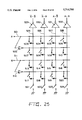
- FIG. 25 is a circuit diagram showing the semiconductor device of the fourteenth embodiment.
- FIG. 26 is a circuit diagram showing the semiconductor device of the fourteenth embodiment.
- FIG. 27 is an exemplary view showing a data retrieval system using the ROM of the invention.
- FIG. 28 is an exemplary view showing a hybrid type system using the ROM of the invention.
- FIG. 29 is an exemplary sectional view showing the form of a silicide region.
- FIG. 30 is a circuit diagram of a semiconductor device having a means for the time of writing completion and a means for finishing writing.
- FIG. 31 is a circuit diagram showing an example of a decoder based on the invention.
- FIG. 32 is a graph showing the reliability of an antifuse after writing.
- FIG. 33 is a graph showing the failure occurrence rates of the antifuse after writing.
- FIG. 34 is a view showing the structure of a single power source power conservation high-speed writing circuit of the thirteenth embodiment.
- the first embodiment of the invention is for a device having a structure shown in FIGS. 1 and 2, and by causing a silicide reaction to progress at a speed of 10 m/sec, a silicide region conducted through upper and lower conductors is generated in a selected cell. If the cell in which this silicide region is formed is "1" and a cell having no silicide is "0", binary values can be stored.
- the semiconductor device of the invention was formed in the following way.
- a silicon base plate having a p type layer was prepared, an n + drain area 6 was formed by a generally known NMOS process, and thereafter a SiO 2 film 7 was formed by means of a CVD, an almost square contact hole with one side 1 ⁇ m was opened.
- non-doped hydrogenated amorphous silicon 8 of 100 nm was formed by means of a plasma CVD.
- the conditions were as follows:
- the base plate was moved from a CVD chamber to another via a carrying chamber of inert atmosphere.
- a tungsten film 9 was formed with thickness of 0.5 ⁇ m under the following conditions:
- the base plate was extracted from a multichamber system and an amorphous film and a tungsten film were formed in patterns shown in FIG. 2 by means of photolithography. Then, a film A110 for wiring was formed by means of RF/DC coupling sputtering and patterned.
- the conditions for Al film formation were as follows:
- the resistance of a cell was measured prior to information writing, and a resistance value was 2 to 3 G ⁇ when a voltage applied to the amorphous silicon film was 6V. Then, the cell was broken down because of a silicide reaction when 17V was applied with a tungsten side as a positive potential and the ON resistance value of the cell including the MOS transistor was 1 k ⁇ (an amorphous silicon layer memory element was about 5 ⁇ ).
- a sample having almost the same structure as the above-described sample but with the thickness of amorphous silicon (a-Si) changed to 500 ⁇ was made.
- writing was allowed with a writing voltage 9V, writing time 50 nsec. and a writing current 7 mA.
- a a-Si film was formed by means of a bias sputtering method and a sample was made.
- the sputtering conditions were as follows:
- a sample was made by forming a tungsten film after the amorphous silicon was formed on the drain area 6 and patterned by means of photolitography. This sample broke down at a silicide reaction speed of 8 m/sec.
- Variance in resistance values for cells were statistically compared, and it was found that the sample as the example of comparison having a silicide speed within 10 m/sec. showed variance and failures twice as big as that of the embodiment having a speed of 10 m/sec or higher.
- FIG. 10 is a sectional view showing the cell structure of a device in the second embodiment of the invention.
- the characteristic of the embodiment lies in the fact that a sandwiching structure of metal/amorphous silicon/metal is buried on a substrate conductor in the contact hole, an upper surface thereof is made flat and a wiring is provided. According to the embodiment, it will be possible to provide devices in great quantities and inexpensively by forming a memory element of a size smaller than a minimum processing dimension and achieving high integration of cells and reduction in the number of masks. A sample for the embodiment was made in the following way.
- a base plate 50 in which a NMOS transistor was formed was prepared and a contact hole of 0.5 ⁇ m was opened.
- Tungsten (W) films 54' were selected and accumulated only in the contact hole by using WF 6 gas, etc.
- an amorphous silicon film 53 was selectively formed in a base plate temperature of 200° C.
- W 54 By selectively depositing W 54 on the amorphous silicon film again, an amorphous silicon memory element having a sandwiching structure was formed in the contact hole.
- These films were continuously formed without being exposed to air by using the multichamber system.
- a wiring 55 made of Al--Si--Cu was formed, and a sample was completed by adding a pashvasion film.
- a writing voltage can be directed in any direction and a freedom for designing a writing driving circuit can be expanded.
- a writing speed improved more than the sample of the first embodiment by 10 to 40%.
- Leakage of a current was reduced more than the sample of the first embodiment by 10 to 40% as well.
- Wiring capacity was reduced by 10 to 20%.
- FIG. 11 shows a device in the third embodiment of the invention.
- the embodiment provides a 2 terminal cell using a diode as a flow rectifying element and is devised to reduce processes and costs and to realize high integration using a process only of wiring film forming and patterning.
- FIG. 11(a) shows a structure thereof
- FIG. 11(b) a circuit
- FIG. 11(c) a sectional view
- 62 and 62' are wirings which are bit lines
- 68 a p + layer 69 n - layer and 70 n + layer, constituting a diode (p + n - n + ).
- 71 is a metal layer silicided with amorphous silicon
- 72 an amorphous silicon layer and 60 and 60' upper part wirings which are word lines.
- An electrically conductive film made of Al and Cr for a substrate wiring was formed on a base plate having an insulated surface. Films of p + type polysilicon, n - type polysilicon, N + type polysilicon, Ti and amorphous silicon were continuously formed thereon by means of the multichamber system.
- bits from 62 to 72 were patterned by means of reactive ion etching.
- etchings were eliminated from layers 68 to 72 excluding one 62 of laminated patterns remaining in a striped form by using CF 4 gas and O 2 gas in accordance with the width of an upper part wiring pattern and an island-like laminated body 61 (or 68 to 72) was formed.
- an almost flat interlayer insulating film was formed by means of etchback using an oxided formed film and a resist.
- the a-Si layer 72 was exposed, a natural oxided film was eliminated by using diluted hydrofluoric acid under nitrogen atmosphere, cleansed by superpure water, carried under nitrogen atmosphere, the base plate was moved to a metal formed film chamber and a Cu wiring was formed.
- the structure of ROM in FIG. 19 can be formed by complete self-alignment during IC processing. For instance, in FIG. 19, a wiring 385 layer, an N + layer 386, a P layer 387, an amorphous semiconductor layer 388 and a metal layer 389 are continuously formed, and these are etched together by a wiring pattern of a longitudinal direction. Then, a peripheral part is covered by an insulating film such as a silicon oxided film and the like, the film of the wiring 382 is formed after this part is made flat, and this time etching is carried out up to the very vicinity of lowest wirings 385 and 384 by means of a wiring pattern orthogonally crossing the above wiring pattern. Lastly, by covering it by an insulating film a ROM part shown in FIG. 19 can be formed.
- 201, 203, 207, 211, 213 and 217 are metals while 202 and 212 are P type amorphous silicon having an impurity density of 10 18 cm -3 which becomes an antifuse.
- 204 is P type polycrystal silicon having an impurity density of 10 20 cm -3
- 205 is 3 ⁇ 10 17 cm -3 P type polycrystal silicon
- 206 is 10 20 cm -3 N type polycrystal silicon.
- PN added to the antifuse is in a direction opposite to that in FIG. 21(a)
- 214 is N type polycrystal silicon having an impurity density of 10 20 cm -3
- 215 is 3 ⁇ 10 17 cm -3
- 216 is 10 20 cm -3 P type polycrystal silicon.
- amorphous semiconductors 202 and 212 are formed on a polycrystal semiconductor constituting a diode.
- the amorphous semiconductor can be formed by means of a low temperature CVD or a sputter.
- a low temperature CVD conditions for film formation are that SiH 4 is 3 sccm and Ar is 320 sccm, a power of 180 MHz and 150 W is applied to an electrode for exciting plasma, plasma of 10 mTorr is excited, a base plate is caused to float and a temperature is set at 300° C.
- a P type target having an impurity density of 10 20 cm -3 is simultaneously film-formed on the base plate by means of sputtering at this time, an amorphous silicon film doped to a P type having an optional density of 10 16 to 10 20 cm -3 by a target bias can be formed.
- Conditions for forming a polycrystal silicon film are that SiH 4 is 1 sccm, Ar is 320 sccm, a power of 180 MHz and 150 W is applied to an electrode for excting plasma, plasma of 10 mTorr pressure is excited, the base plate is caused to float and a temperature is set at 300° C.
- a P or N type target having an impurity density of 10 20 cm -3 is simultaneously film-formed on the base plate by means of sputtering, and thereby a polycrystal silicon film doped to an optional density of 10 16 to 10 20 cm -3 by a target bias this time can be formed.
- Each film thus formed is etched by means of, as described above, RIE by self-alignment.
- a semiconductor device was made with a diode part as a N + pp + type according to a procedure shown in FIG. 13.
- the structure of this antifuse is one in which this semiconductor device was formed by self-alignment by means of a technique for selecting and growing a metal on a semiconductor and one for selecting and growing a semiconductor on a metal.
- FIG. 13 shows a forming process by means of this self-alignment.
- a metal layer 220 is film-formed and etched to a predetermined pattern by RIE. This method allows easy film forming by normal sputtering. Then, films of N type polycrystal silicon 221 having an impurity density of 10 20 cm -3 , P type polycrystal silicon 222 having an impurity density of 3 ⁇ 10 17 cm -3 and P type polycrystal silicon 223 having an impurity density of 10 20 cm -3 are formed by means of a plasma CVD method.
- Conditions for film formation of polycrystal silicon are that SiH 4 is 1 sccm, Ar is 329 sccm, a power of 180 MHz and 150 W is applied to an electrode for exciting plasma, plasma of 10 mTorr pressure is excited, a base plate is caused to float and a temperature is set at 300° C.
- a P or N type target having an impurity density of 10 20 cm -3 is simultaneously film-formed on the base plate by means of sputtering, and thereby polycrystal doped to an optional density of 10 16 to 10 20 cm -3 by a target bias this time can be film-formed (FIG. 13(a)).
- a semiconductor layer 226 is formed only on the metal 225 by means of the technique for selecting and growing a semiconductor on a metal.
- a metal 227 is then formed only on the semiconductor layer 226 by means of the technique for selecting and growing a metal on a semiconductor, and thus a structure shown in FIG. 13(d) is brought about. Selection and growth of the metals 225 and 227 can be performed by the method described in the second embodiment.
- a device in the fifth embodiment of the invention is constructed by a cell having a flow-rectifying element of a Schottky diode and a memory element of an antifuse type.
- FIG. 14 is an exemplary view illustrating the device of the embodiment. The structure of the device of the embodiment will be explained in terms of a manufacturing process. First, as a base plate 230 having an insulating film surface, W was film-formed, as a metal 231 which is a substrate conductor, on a silicon wafer having SiO 2 (FIG. 14(a)).
- an insulating film 232 was formed after the W film was patterned and a contact hole was opened.
- a P type polysilicon layer 233 and a P + type polysilicon layer 234 were deposited.
- the P layer 233 was polyslicon having a layer thickness of 0.2 ⁇ m containing boron of about 3 ⁇ 10 17 cm -3 while the P + layer was polysilicon having a layer thickness of 0.1 ⁇ m containing boron of about 1 ⁇ 10 20 cm -3 (FIG. 14 (b)).
- a-Si film 236 P type hydrogenated amorphous silicon containing boron of about 1 ⁇ 10 18 cm -3 was used.
- the layers 233 and 234 were easily formed in the same chamber.
- the device of the embodiment allows high-speed writing and generates no malfunction.
- no upper layer is shown in FIG. 14, this may be made by forming the W film 237 itself in a wiring-like pattern or another conductive layer may be formed.
- FIG. 15 is a view showing a device of the sixth embodiment of the invention. There is shown a method of short-circuiting between optional ones of a number of wirings.
- Amorphous semiconductors 255, 256, 257 and 258 are provided being sanwiching between metal wirings 251 and 252 and conductor wirings 253 and 254.
- These metal wirings 251 and 252 are, for instance tungsten and tantalum, but other metals may be used.
- the conductor wirings 253 and 254 may be metals or semiconductors having an impurity doped high density.
- the metal wiring 251 is connected to a power source 261, the metal wiring 252 to a power source 262, the conductor wiring 253 to a grounding electrode and 254 to a power source 263.
- the power source 261 outputs a voltage smaller than the power sources 262 and 263.
- a voltage of V DD is applied to the amorphous semiconductor area 255 while a voltage of VDD/2 is applied to those 256 and 258 and no voltage is applied to 257.
- the thickness of the amorphous semiconductor layer and the impurity density are preset so as to keep a voltage for causing breakdown in the amorphous semiconductor within V DD /2 to V DD , breakdown will occur only in the amorphous semiconductor 255. Thus, only the amorphous semiconductor will react with the metal wiring 252 and become a low resistance silicide.
- an amorphous semiconductor area on a optional spot can be changed to a low resistance silicide by changing voltages applied to the metal wirings and the conductive body wirings. This means that connection and insulation of selected wirings can be optionally determined.
- FIG. 15(b)) shows a equalizer circuit used at this time.
- Resisters 270, 271, 273 and 274 provide resistance components on the wirings 252, 253 and 254.
- a resistor 272 is ON resistance of the antifuse 255 and 257 indicates an antifuse 257.
- resistance per a wiring length to adjacent antifuse 1 ⁇ m is only about 0.055 ⁇ when antifuses are arrayed at an interval of 1 ⁇ m.
- the ON resistance 272 of the antifuse is several ten ⁇ , there is little voltage reduction on the resistor 270 by a current flowing through the resisters 270, 272 and 273. Thus, since a breakdown voltage is applied only to the antifuse 275, the antifuses can be selectively turned to conductive states.
- a voltage produced by the power source 261 was V DD /2.
- other voltages can be produced as long as they are smaller than V DD .
- a voltage applied to the wiring was positive. This is because migration of metal atoms into the semiconductor is brought about and a conductive state of low resistance is easily realized if electrons are caused to flow from the metal side to the amorphous semiconductor at the time of breakdown.
- Reaction between the metal and the amorphous semiconductor is caused to occur, as shown by this example, by supplying a current to a specified amorphous semiconductor layer.
- a current may be supplied to a specified amorphous semiconductor layer.
- Reaction can also be produced by supplying a current while giving heat from the outside. Using both, reaction will be made easier and high-speed connection between the wirings will be achieved.
- wirings made of metals were shown. However, all the wirings can be made of other than metals, and instead metal layers brought into contact with the amorphous semiconductor layer may be sanwiching between the wirings.
- the 2 terminal cell of the embodiment has, as described above, a simple structure. Thus, it can be manufactured at low costs, either polarity can be selected for a voltage to be applied, and since the wiring resistance of the word line is smaller than the ON resistance (a resistance value of a broken down memory element) of the memory element, there will be no voltage decline on the word line.
- connection and insulation between the wirings can be arbitrarily determined by means of a voltage applied between two wirings, and thus in a semiconductor integrated circuit a method of connecting elements can be set after an IC manufacturing process.
- a method of connecting elements can be set after an IC manufacturing process.
- wirings connecting these circuits can be freely determined depending on each user's purpose.
- programmable logic array PLA
- FIGS. 16 and 17 The seventh embodiment of the invention is shown in FIGS. 16 and 17.
- FIG. 16 shows a circuit structure
- FIGS. 17(a) and 17(b) are a plan view and a suctional view of a memory element periphery.
- a memory element of the invention is used on the intersected point of a control gate matrix for determining signals applied to the control gates (289, 290 and 291) of a neuron MOS transistor ( ⁇ MOS).
- the bit lines 281 and 282 of the control gate matrix are held at a specified high or low potential during ⁇ MOS operation.
- a memory element antifuse (AF) is used.
- 286 to 288 are diodes.
- a writing operation can be performed by the same way as in the case of the above-described embodiment using bit lines 283 to 285.
- a voltage applied to the control gate according to the breakdown of the memory element controls a current flowing between the source drains (between V W and V B ) of the ⁇ MOS transistor by means of capacity coupling with a floating gate (292).
- the potential of the floating gate 292 becomes a linear sum of voltages applied to the control gate, and thus the ⁇ MOS can singly treat multivalues.
- 300 is a silicon base plate
- 301 is SiO 2
- 291 is a control gate of N + type polysilicon
- 292 is a floating gate of N + type polysilicon
- 302 is an interlayer insulating film
- 304 is a metal to be silicided
- 305 is hydrogenated amorphous silicon
- 282 is an upper layer wiring as a bit line
- 303 is P type polysilicon for forming a PN diode
- 285 is a wiring of Al, etc.
- a programmable logic capable of treating multivalues can be made extremely small.
- the eighth embodiment of the invention is a modified example of the semiconductor device shown in FIGS. 1 and 2.
- the semiconductor layer 8 shown in FIG. 2 is one injected with ions and the pashvasion film on the wiring 10 is one formed at a low temperature of about 250° C. or less.
- a speed for a silicide reaction improved by about 20%.
- it is effective not only for increasing a writing speed but also for reducing a writing voltage, and for higher integration and reduction in power consumption.
- a silicon base plate having a P type layer was prepared, an n + drain area 6 was formed by means of a generally known NMOS process, a SiO 2 film was formed by means of CVD, and then an almost square contact hole with one side 1 ⁇ m was opened. Then, by means of plasma CVD non-doped d hydrogenated amorphous silicon of 50 nm was formed. Conditions were as follows:
- tungsten film having a thickness of 50 nm was formed under the following conditions:
- the base plate was extracted from the multichamber system and the amorphous silicon and tungsten films were patterned in forms shown in FIG. 2 by means of lithography.
- Metals of Ta, etc., other than W can be used.
- a first round of ion injection into boron was performed via the metal with an acceleration voltage 25 keV and a dozing amount 5 ⁇ 10 12 cm -2 .
- a second round of ion injection was performed by using Si, Ar, P and As with acceleration voltages 50 to 110 keV and ions were injected into the amorphous layer.
- Al for wiring was film-formed by means of RF-DC sputtering and patterned.
- Conditions for Al film formings were as follows:
- a device in the ninth embodiment is provided with a structure shown in FIG. 12, wherein a-Si layers as first semiconductor areas indicated by 202 and 212 are non-doped layers and 205 and 215 as parts of second semiconductor layers are a P type a-Si layer and a N type a-Si layer.
- the film thickness of the non-doped a-Si layers 202 and 212 is 50 nm
- that of the P type a-Si layer 205 is 70 nm having a density of 5 ⁇ 10 17 cm -3
- that of the N type a-Si layer 215 is 60 nm having a density of 2 ⁇ 10 17 cm -3 .
- resistance between metals 203 and 207 in which a flow-rectifying barrier is formed is lower than that between conductors, that is, metals 201 and 203, and similarly resistance between metals 213 and 217 in which a flow-rectifying barrier is formed is lower than that between metals 211 and 213.
- a silicide reaction occurs on the a-Si layers 202 and 212 while no silicide reaction occurs on a-Si layers 204, 205 and 206 on a lower part and those 214, 215 and 216, and no destruction of PN connection was found. This is conceivably due to the fact that by reducing resistance on the lower part a-Si layers no current is caused to flow locally and a current density is reduced.
- the above-described film thickness and density are used, others can be used as long as resistance of the second semiconductor areas 204, 205 and 206 and that of those 214, 215 and 216 are set lower than that of the a-Si layers of the first semiconductor areas 202 and 212.
- a material for a rectifier having a flow-rectifying barrier a-Si is used, the device is constructed by the same materials as 202 and 212 and thus a silicide reaction is generated.
- polySi and a single crystal Si can be used.
- the size of resistance is realized depending on film thickness and density.
- pattern dimension for connection between the metals and the first semiconductor areas that is, the patterns of the upper parts 201 and 202 can be made smaller than the lower part patterns 203 to 207 and likewise the patterns of the upper parts 211 and 212 can be made smaller than the lower part patterns 213 to 217.
- a highly integrated memory can be operated stably and without any failures.
- a semiconductor device of the tenth embodiment having a structure shown in FIG. 12 is one, wherein a-Si layers of the first semiconductor areas 202 and 212 are P type ion injected layers and parts 205 and 215 of the second semiconductor areas are non-doped a-Si layers.
- resistance between the metals 203 and 207 as conductors that is, resistance of the second semiconductor layers is set higher than that between the metals 201 and 203 as conductors, that is, resistance of the first semiconductor areas and likewise resistance between the metals 213 and 217, that is, resistance of the second semiconductor areas, is set higher than that between the metals 211 and 213, that is, resistance of the first semiconductor areas.
- a rectifier of the device As a rectifier of the device, a PIN type is used. However, a Schottky type rectifier can also be used. By this structure of the element a stable operation is realized and thus suitable to the highly integrated memory.
- a device in the eleventh embodiment of the invention having a structure shown in FIG. 12 is one, wherein the metals 203 and 213 are made of the second semiconductor areas 204 and 214 and metal materials which generate no silicide reaction.
- the metal materials generating no silicide reaction a Al--Si alloy was used, and it was found that even with an impurity density of the second semiconductor areas 204 and 214 set at 5 ⁇ 10 17 cm -3 the second semiconductor areas 204, 205 and 206 or 214, 215 or 216 did not form a silicide reacting with the metals 207 and 203 or 217 and 213.
- a method of using the metal materials not to be silicided in the embodiment is very effective, because it prevents the second semiconductor areas from reacting by mistake as in the case of the method described in the ninth and tenth embodiments.
- all the metals 203, 207, 213 and 217 are made of metals not forming a silicide, it is possible to use these materials for parts thereof. For instance, by forming 203 and 213 of a plurality of electrically conductive materials, only parts thereof brought into contact with the second semiconductor layers can be made of the metals not to be silicided.
- FIG. 18 shows the twelfth embodiment of the invention. It is a known fact that all logical functions can be expressed by coupling between AND and OR logics.
- a circuit in the embodiment is a so-called programmable logic array (PLA) capable of realizing an optional function by preparing AND an OR circuits beforehand and optionally determining connection and insulation between the I/O wirings of these circuits after an IC manufacturing process.
- PLA programmable logic array
- XOR exclusive logical OR
- 341 and 342 are two input AND circuits and 348 is a two input OR circuit.
- 339 and 340 are inverters. These circuits can be made by means of a normal IC processing technique.
- 330 to 337 an 343 to 347 are I/O wirings. These wirings may be metals or electrical conductors made of other than these.
- the wirings 330 to 333 are formed on layers different from those on which the wiring 334 to 337 are formed and the wirings 343 and 344 are formed on layers different from those on which the wrings 345 and 346 are formed.
- FIG. 18(b) shows the structure of an intersecting portion 338 between the wirings 330 and 337 shown in FIG. 18(a).
- a layer indicated by 349 is a metal layer and an amorphous semiconductor layer 350 is in contact with this layer.
- a metal layer 349 it does not matter whether a metal layer 349 is provided or not.
- a plurality of structures in which the amorphous semiconductor layer and the metal layer are in contact with each other may exist between the wirings 330 and 337.
- the wirings 330 and 337 can be electrically selected and connected.
- Black dots 338 in FIG. 18(a) indicate that wirings have been selectively connected and these connections can be selectively made in the last stage of an IC manufacturing process or after all processes are finished.
- interwiring connection when interwiring connection is performed as in FIG. 18(a), the value of an output 347 is an exclusive logical OR between inputs A and B.
- interwiring connection is performed in order to realize exclusive logical ORing. It is possible, however, to perform all logical calculations for the two inputs.
- FIG. 19 shows a read-only memory (ROM) of the thirteenth embodiment.
- Switches 390 and 391 in the drawing can be realized, as shown in FIG. 20(a), by using a NMOS, but these may be constructed, as shown in FIG. 20(b), by CMOS inverters.
- a voltage of a node 401 in FIG. 20(a) a power source voltage appears through a transistor 402 when ⁇ 1 is "1" and a grounding voltage appears through a transistor 403 when E1 is "0".
- a grounding voltage appears on an output terminal 405 with ⁇ 1 set to "1" and a power source voltage appears thereon with E1 set to "0".
- Switches 392 and 393 can set nodes 370 and 373 to three states, one in which these nodes are connected to a power source voltage terminal, one in which these are connected to a grounding terminal and floating one, and these switches can be realized, as shown in FIG. 20(c), by using NMOS.
- these may be constructed by CMOS inverters and NMOS.
- a transistor 407 is cut off when ⁇ 2 is set to "0" and a node 410 is caused to float.
- a power source voltage appears on the node 410 through the transistors 408 and 407 by setting E1 to "1” and a grounding voltage appears thereon through the transistors 409 and 407 by setting ⁇ 1 to "0".
- a node 413 is caused to float by setting ⁇ 2 to "0".
- a grounding voltage by setting ⁇ 1 to "1” and a power source voltage by setting ⁇ 1 to "0” appears on the node 413.
- NMOSes 402, 403, 408, 409 and 407 may be PMOS or analog switches having CMOS structures shown in FIG. 20(e).
- analog switch having the CMOS structure the same voltage as on a node 14 appears on a node 415 by setting E1 to "1".
- FIG. 21 shows an equalizer circuit of FIG. 19.
- FIG. 19 will be explained by using this equalizer circuit.
- a switch 467 indicates an insulated state of the amorphous semiconductor layer 388 shown in FIG. 19 by means of an equalizer circuit.
- switches 466, 468 and 469 indicate amorphous semiconductor layers and all these switches are in OFF states before writing.
- a PN diode 471 indicates PN connection between 387 an 386 shown in FIG. 19. The same is true for PN diodes 470 and 473.
- 453 and 456 are word lines while 460 and 464 are bit lines.
- Switches 453 and 456 are those shown, for instance in FIG. 20(a) or in FIG. 20(b), and switches 458 and 462 are those shown, for instance in FIG. 20(c) or in FIG. 20(d).
- 457, 477, 479 and 481 are inverters constituting a sense amplifier for amplifying signals of bit lines and determining "1" or "2" thereof.
- the potential of the bit line 464 is set to a power source voltage V DD .
- V DD is applied between the word lines 456 and 453 and the bit line 464 at this time, the direction of this voltage is a reverse bias for PN connections 471 and 473. If resistance at the time of a reverse bias for the PN connections is set sufficiently larger than that of the amorphous semiconductor layer, most of voltages applied between the word lines 456 and 453 and the bit line 464 are applied to the PN connections. Thus, no breakdown occurs in the amorphous semiconductor areas indicated by the switches 467 and 469 and resistance on the layers thereof is always kept high.
- V DD is applied between the word line 456 and the bit line 460 and a potential difference between the word line 456 an the bit line 464 disappears.
- V DD is applied between the word line 456 and the direction thereof is forward for the PN connection 472
- resistance thereon at this time is sufficiently lower compared with that in the amorphous semiconductor area indicated by the switch 468 and most of the V DD is applied to the amorphous semiconductor area indicated by the switch 468. Therefore, breakdown occurs in the amorphous semiconductor area indicated by the switch 468, a low resistance silicide is generated and the switch 468 is equivalently switched ON.
- "1" has been written in a memory cell on an intersecting portion between the word line 456 and the bit line 460.
- FIG. 30 A structure which allows simultaneous writing by solving this problem is shown in FIG. 30.
- FIG. 30 shows a memory circuit to which a detecting circuit for detecting completion of writing by a current flowing to each bit line is added.
- This circuit monitors the potentials of bit lines 859 to 861 during writing. The instance a writing operation is started, the potential of the word line 858 and those of the bit lines 859 to 861 connected to the memory cell into which writing is performed are V DD and grounding potentials respectively.
- the memory cell 854 becomes a low resistance silicide after writing is started, a large current is caused to flow, the potential of the bit line 859 increases and exceeds Von (threshold values of the inverters 863 and 862).
- the detecting circuit 850 switches the NMOS 862 OFF after detecting this, switches the PMOS 864 and 863 ON and charges the bit line 859 to V DD and then writing into the memory cell 854 is finished.
- the voltage V DD is applied again to the other memory cells 855 and 856 on the same word line and writing is performed sequentially. It is possible, by providing this circuit for each word line, to simultaneously write into a plurality of memory cells.
- the antifuse of the invention usually needs two kinds of power sources, a circuit operation voltage and a writing voltage. EEPROM also needs two voltage sources and thus a boosting circuit, etc., are incorporated. For the antifuse of the invention two power sources may be prepared by the same method.
- FIG. 34 shows an example of an antifuse writing circuit capable of high-speed writing using a single power source and consuming low power.
- the circuit in FIG. 34 is a single power source low power consumption high-speed writing circuit having a circuit for instantaneously increasing a voltage between a bit line 911 and a word line 910 over one causing a breakdown of amorphous silicon by applying a pulse input V 4 to the word line 910 via an electrostatic capacitor C 2 (905).
- 901 is a PMOS transistor and 902 and 903 are NMOS transistors.
- antifuse writing can be performed in the following way:
- V 3 is lowered to the grounding potential and V 1 is set to V DD .
- V 1 may be kept fixed to the grounding potential.
- a pulse voltage of V DD is inputted to V 4 .
- the electrostatic capacitor C 2 is designed smaller by 1/5 compared with C 1 .
- the potential of the word line instantaneously increases to about 2V DD
- a voltage of 2V DD is instantaneously applied between the word line 910 and the bit line 911 and thus breakdown of amorphous silicon occurs.
- electric charges accumulated in the ccapacitor C 1 is caused to flow to the bit line fixed at the grounding potential via the antifuse by the breakdown, a silicide reaction progresses and writing is performed.
- the potential of the word line may be set to either the grounding potential or V DD .
- a writing current automatically stops flowing by means of discharging of the electrostatic capacitor C 1 . Therefore, consumption of power caused by needlessly supplying a current to the antifuse in which low resistance has been obtained is eliminated, making it possible to perform writing consuming less power. Also, by dividing electrostatic capacity between the word line and grounding potentials into two serial capacities, large capacitor C 1 and small capacitor C 2 , equivalent capacity between the word line and grounding potentials is made small. As a result, the quantity of electric charges charged/discharged per writing is reduced and writing with power consumption still more reduced can be performed.
- a time necessary for increasing the potential of the word line during writing can be made almost equal to a time for changing C 1 to V DD , a time for charging can be shortened more compared with in a case where the word line is charged to 2V DD against the grounding potential.
- the large capacitor C 1 is short-circuited by setting V 2 to V DD .
- the capacity of the word line potential can be made smaller compared with that of the grounding potential, making it possible to perform reading at a very high speed.
- the transistor 902 is NMOS. However, PMOS may be used. In this case, for the above-described operation, the grounding potential is inputted instead of V DD and V DD is inputted instead of the grounding potential.
- V 4 In the case of generating a pulse V 4 inputted at the time of writing, an effect of instantaneously increasing potentials via the capacitors can be similarly utilized. This makes it possible to instantaneously increase the potential of V 4 higher than V DD . Even when a writing voltage is designed larger than 2V DD , the potential of the word line can be increased to the writing voltage by generating large V 4 . In the circuit, any method of generating a pulse V 4 can be used. V 4 has a pulse waveform of a voltage V DD . However, waveforms are not limited to this.
- the single power source writing circuit is shown as an example of writing by means of generation of a writing voltage via the capacitors
- inputs to V 1 , V 2 , V 3 and V 4 need not to have the same voltage amplitude.
- the input V 4 has an effect of increasing the potential of the word line via the static capacitor, this can be connected to the word line not via C 1 but via C 2 allowing to obtain the same effect.
- insulating films such as silicon oxided films and the like.
- a thick oxided film may be formed by means of CVD, etc., after an insulating film is formed of a liquid phase such as superpure water in which ozone is dissolved, hydrogen peroxide water, solution mixing sulfuric acid and hydrogen peroxide water and the like on the border surface.
- writing may be performed while cooling the base plate by liquid or fluids.
- FIG. 22 shows an equalizer circuit wherein only amorphous semiconductor areas indicated by switches 466 and 468 are low resistance silicides (that is, a content of a memory is "1").
- amorphous semiconductor areas indicated by the switches 466 and 468 are low resistance silicides.
- amorphous semiconductor areas may be low resistance silicides.
- switches 450, 454, 458 and 462 are all set to the grounding electrode side and all the word lines and bit lines are grounded.
- the potential of the word line 456 is set to the power source voltage V DD by, for instance, setting the switch 454 to the power source side. Since the switch 468 is in an ON state and the PN connection is biased in a forward direction, a current is caused to flow from the word line 456 to the bit line 460, increasing the potential. If the thresholds of inverters 477 and 481 are set higher than the grounding potential, when the potential of the bit line 460 exceeds the threshold of the inverter 477, the inverter 477 is reversed, followingly an inverter 475 is also reversed and the value of an output node 474 is changed from "0" to "1". By means of this output change, it can be known that the amorphous semiconductor layer indicated by the switch 468 is actually a low resistance silicide. That is, that information stored in the memory cell is "1" can also be read.
- the switch 466 is short-circuited.
- the potential of the word line 453 is the grounding potential and that of the bit line 460 is positive, the direction of the PN connection 470 is reversed and thus no current is caused to flow from the bit line 460 to the word line 453.
- bit line 464 As for the bit line 464, since the switch 469 is OFF, no current flows between the word line 456 and the bit line 464 and thus the potential of the bit line 464 is kept at the grounding potential. Therefore, a output terminal is always kept at "0", and from this it can be known that the amorphous semiconductor layer maintains an insulated state. That is, that information stored in the memory cell is also "0" can be known.
- information stored in a memory cell in an optional place can by read by the following three steps:
- a content stored in the memory cell can be known by means of an output from a sense amplifier connected to each bit line).
- the bit line increases slightly more than the grounding potential, by latching a result of reading thereof after information of "1" is read, the word line can be separated from the voltage source thereafter. Thus, power consumption can be reduced.
- two word lines and two bit lines are used. However, it is needless to say that the numbers of these may be optionally selected. In this case also, writing into an optional memory cell can be performed and information stored in an optional memory cell can be read.
- the characteristic of this ROM is that since information is read through a low resistance silicide and the forward-direction PN connection when the memory element is in a conductive state (information of "1" is stored), reading can be performed at a very high speed.
- a MOS transistor which is a surface device was used as a switch element and thus a current was small.
- a current flowing to the forward-direction PN connection increases in an exponential functional manner and a larger current compared with the MOS transistor as the surface device is supplied, making it possible to attain a high speed.
- this ROM can be formed by complete self-alignment during IC processing.
- the wiring 385, the N + layer 386, the P layer 387, the amorphous semiconductor layer 388 and the metal layer 389 are continuously formed and these are etched together in the wiring pattern of a longitudinal direction.
- the layer of the wiring 382 is film-formed, and this time etching is carried out up to the vicinity of the lowest wirings 384 and 385 in a wiring pattern orthogonally crossing the above-described wiring pattern.
- the ROM part in FIG. 19 can be structured.
- the memory cells can be arrayed at the intervals of the wirings end thus high integration is allowed. Since these wiring intervals are determined by minimum processing dimension during IC manufacturing, ROM having an extremely high density can be obtained. If this minimum processing dimension is L, an area occupied by one memory cell is 4L 2 . This is a very high level of integration never attained by the ROM of a conventional type using the MOS transistor for two-dimensionally making an element on a base plate plane.
- the switches 450, 454, 458 and 462 in FIG. 21 may be composed using decoders shown FIG. 31. This is a circuit wherein one is selected from four outputs 489, 490, 491 and 492 and by setting only this output to "1" the other outputs are set to "0".
- Black dots 484 indicate that connection between the wirings 482 and 483 is in an electrically short state.
- a and B are inputs 493 and 494 is an inverter.
- 485, 486, 487 and 488 are AND circuits and the output 489 of 485 is “1" only when A is “0" and B is "1".
- the output 490 of 486 is “1" only when A is “0” and B is "1".
- the output 491 of 487 is “1" only when A is “1" and B is "0".
- the output 492 of 488 is “1" only when A is "1" and B is "1".
- a floating state can be realized by connecting a NMOS transistor to each output line and setting a signal inputted to a gate thereof to "0".
- optional output lines can be selected from a larger number of output lines.
- the word lines and the bit lines may be selected by means of the decoder. It is needless to say, however, that the same can be performed by using a random logic instead.
- the structure of the memory cell shown in FIG. 19 may be made by sandwitching a high-density layer 495 between the amorphous semiconductor and the P layer as shown in FIG. in FIG. 23(a). In this way, after reaction between the metal and the amorphous semiconductor is finished, by means of a contact between the low resistance silicide and the high-density layer contact resistance can be reduced more and a large forward-direction current can be caused to flow.
- PN connection is used in the ROM
- a Schottky connection between a semiconductor 496 and a metal 497 maybe used instead as shown in FIG. 23(b).
- a memory cell can be provided with a flow-rectifying characteristic in this case.
- the directions of the PN connection and the Schottky connection may be reversed if a power source voltage is changed between positive and negative depending on cases.
- the fourteenth embodiment of the invention is shown in FIG. 24.
- FIG. 24 shows a circuit for outputting logical OR between two inputs.
- 503 to 510 and 513 to 520 are switches and PN diodes and these indicate amorphous semiconductor layers and PN connections sanwiching between word lines 501 and 511 and bit lines 525, 526 and 528.
- the switches are ON and this indicates that the amorphous semiconductor layers and metal layers are selectively reacted and these are low resistance silicides.
- Switches 521 to 524 are for initializing each bit line to a grounding potential, and by switching these switches OFF and causing the bit line to float after initialization a calculation result appears in each bit line.
- FIG. 25 shows a circuit for reversing the output of each logical OR in FIG. 24 by means of inverters 529, 530, 531 and 532 and outputting this.
- An output reversed by the inverter 529 is indicated by logical AND between the reverse of A and the reverse of B.
- An output reversed by the inverter 530 is indicated by logical AND between the reverse of A and B.
- An output reversed by the inverter 531 is incidated by logical AND between the reverse of B and A.
- An output reversed by the inverter 532 is indicated by logical AND between A and B. That is,only one of the four outputs 529 to 532 is "1" for each of the four combinations of A and B and the remaining three are "0", realizing a decoder.
- FIG. 26 shows an example of realizing exclusive logical OR between, for instance two inputs by using the circuit for calculating logical AND in FIG. 25 and the circuit for calculating logical OR in FIG. 24.
- 533, 534, 535 and 536 are the same output lines as in FIG. 25. Connections between these lines and an output line 534 are determined by combinations 538, 539, 540 and 541 of switches and diodes. Since in this example wirings 534 and 535 are connected to a wiring 542, logical OR between 534 and 535 is outputted to 542.
- All logical calculations can be performed by means of combinations between AND an OR.
- Optional logical functions can be realized by combining a logical plane for AND and that for OR, as in the above.
- OR exclusive logical OR
- a circuit for inputting an optional group of signals and outputting an optional group of signals corresponding thereto one to one can be made by using AND and OR planes of multiinputs and multioutputs.
- FIG. 27 shows a data retrieval system using ROM.
- a library retrieval As an example of the data retrieval system, there is available a library retrieval. This is a system for outputting, for instance all related books, by inputting only fields and names of writers one wishes to read out of an immense number of books.
- ROM In order to store a great deal of library data on hardware to which high-speed accessing is allowed, ROM having an extremely high density is necessary.
- this ROM needs to be programmable ROM of a type which allows a user to write information later and thus high-density programmable ROM to which high-speed accessing can be made is necessary.
- a characteristic of a retrieval system in the embodiment lies in the fact that not only a medium for storing information is realized by high-speed and high-density ROM but also a calculating part itself for calculating which data is to be outputted based on inputted data is realized by high-speed an high-density ROM.
- this output information is one for indicating an address of, for instance 625 part in ROM 626, the information of 625 can be outputted to an output line 627.
- a series of these operations makes it possible to read information in ROM corresponding to certain inputs A and B. If these inputs A and B indicate a writer's name of books, all the books by this writer are written in the part 625 in ROM 626 and an address thereof is written in a memory cell connected to the wiring 616, by inputting the name of the writer the books are automatically outputted.
- codes of calculating commands may be inputted and a procedure for executing these commands may be stored in, for instance ROM 625. It is also possible to write various kinds of application software conventionally stored in the magnetic medium in ROM and input command codes for stating the software in the inputs A and B. When the version of the application software is to improved and new software is to be installed again, this can be newly installed by making it impossible to access the old address according to the above-described method.
- the inputs A and B need not be 2 bit, but optional bit number can be selected and the size of the system can be optional.
- FIG. 28 The sixteenth embodiment of the invention is shown in FIG. 28.
- FIG. 28 shows a hybrid type system wherein a highly integrated and high-speed ROM devised by the invention is disposed around a chip having a CPU within and connected directly by a bonding wire.
- CPU instruction codes and various kinds of application software may be all written in this ROM.
- ROM having the above-described data retrieving function may be disposed around the chip.
- a low resistance and highly reliable antifuse it is possible to provide a low resistance and highly reliable antifuse. That is, an occurrence rate of failures can be limited by forming a silicide region with 150 nm or less in width and a highly reliable antifuse can be provided.
- PLA programmable logic array
- FPGA field programmable gate array
Abstract
Description
Claims (37)
Applications Claiming Priority (2)
| Application Number | Priority Date | Filing Date | Title |
|---|---|---|---|
| JP6-277995 | 1994-11-11 | ||
| JP27799594A JPH08139197A (en) | 1994-11-11 | 1994-11-11 | Semiconductor device utilizing silicide reaction |
Publications (1)
| Publication Number | Publication Date |
|---|---|
| US5714795A true US5714795A (en) | 1998-02-03 |
Family
ID=17591167
Family Applications (1)
| Application Number | Title | Priority Date | Filing Date |
|---|---|---|---|
| US08/554,053 Expired - Lifetime US5714795A (en) | 1994-11-11 | 1995-11-06 | Semiconductor device utilizing silicide reaction |
Country Status (2)
| Country | Link |
|---|---|
| US (1) | US5714795A (en) |
| JP (1) | JPH08139197A (en) |
Cited By (30)
| Publication number | Priority date | Publication date | Assignee | Title |
|---|---|---|---|---|
| US5937281A (en) * | 1997-08-05 | 1999-08-10 | Powerchip Semiconductor, Corp. | Method to form metal-to-metal antifuse for field programmable gate array applications using liquid phase deposition (LPD) |
| US6015977A (en) * | 1997-01-28 | 2000-01-18 | Micron Technology, Inc. | Integrated circuit memory cell having a small active area and method of forming same |
| US6087689A (en) * | 1997-06-16 | 2000-07-11 | Micron Technology, Inc. | Memory cell having a reduced active area and a memory array incorporating the same |
| US6096626A (en) * | 1998-09-03 | 2000-08-01 | Micron Technology, Inc. | Semiconductor structures and semiconductor processing methods of forming silicon layers |
| US6104038A (en) * | 1995-06-07 | 2000-08-15 | Micron Technology, Inc. | Method for fabricating an array of ultra-small pores for chalcogenide memory cells |
| US6153890A (en) * | 1996-08-22 | 2000-11-28 | Micron Technology, Inc. | Memory cell incorporating a chalcogenide element |
| US6189582B1 (en) | 1997-05-09 | 2001-02-20 | Micron Technology, Inc. | Small electrode for a chalcogenide switching device and method for fabricating same |
| US6229157B1 (en) | 1996-06-18 | 2001-05-08 | Micron Technology, Inc. | Method of forming a polysilicon diode and devices incorporating such diode |
| US6429449B1 (en) | 1995-06-07 | 2002-08-06 | Micron Technology, Inc. | Three-dimensional container diode for use with multi-state material in a non-volatile memory cell |
| US6440837B1 (en) | 2000-07-14 | 2002-08-27 | Micron Technology, Inc. | Method of forming a contact structure in a semiconductor device |
| US20020179896A1 (en) * | 1995-06-07 | 2002-12-05 | Harshfield Steven T. | Method and apparatus for forming an integrated circuit electrode having a reduced contact area |
| US6531391B2 (en) | 1996-07-22 | 2003-03-11 | Micron Technology, Inc. | Method of fabricating a conductive path in a semiconductor device |
| US6563156B2 (en) | 2001-03-15 | 2003-05-13 | Micron Technology, Inc. | Memory elements and methods for making same |
| US20030160298A1 (en) * | 2002-02-26 | 2003-08-28 | Fujitsu Limited | Anti-fuse and method for writing information into the anti-fuse |
| US6670713B2 (en) | 1996-02-23 | 2003-12-30 | Micron Technology, Inc. | Method for forming conductors in semiconductor devices |
| DE10231646A1 (en) * | 2002-07-12 | 2004-04-08 | Infineon Technologies Ag | Memory cell for permanently storing data has a switching unit with a field effect transistor having a drain region formed as the heating region |
| US20040089917A1 (en) * | 2000-04-28 | 2004-05-13 | Knall N. Johan | Three-dimensional memory array and method of fabrication |
| US20070069276A1 (en) * | 2005-09-28 | 2007-03-29 | Scheuerlein Roy E | Multi-use memory cell and memory array |
| US20080025118A1 (en) * | 2006-07-31 | 2008-01-31 | Scheuerlein Roy E | Method for using a mixed-use memory array |
| US20080025062A1 (en) * | 2006-07-31 | 2008-01-31 | Scheuerlein Roy E | Method for using a mixed-use memory array with different data states |
| US20080025069A1 (en) * | 2006-07-31 | 2008-01-31 | Scheuerlein Roy E | Mixed-use memory array with different data states |
| US20080029844A1 (en) * | 2006-08-03 | 2008-02-07 | Adkisson James W | Anti-fuse structure optionally integrated with guard ring structure |
| US20080101108A1 (en) * | 2006-10-24 | 2008-05-01 | Hajime Tokunaga | Semiconductor device including storage device and method for driving the same |
| US7816189B2 (en) | 1998-11-16 | 2010-10-19 | Sandisk 3D Llc | Vertically stacked field programmable nonvolatile memory and method of fabrication |
| CN101180684B (en) * | 2005-05-24 | 2011-03-30 | Nxp股份有限公司 | Anti-fuse memory device |
| US20120129319A1 (en) * | 2007-03-07 | 2012-05-24 | International Business Machines Corporation | Electrical Antifuse, Method of Manufacture and Method of Programming |
| US8575719B2 (en) | 2000-04-28 | 2013-11-05 | Sandisk 3D Llc | Silicon nitride antifuse for use in diode-antifuse memory arrays |
| US9704960B2 (en) | 2010-09-03 | 2017-07-11 | Semiconductor Energy Laboratory Co., Ltd. | Field effect transistor and method for manufacturing semiconductor device |
| US9754903B2 (en) * | 2015-10-29 | 2017-09-05 | Globalfoundries Inc. | Semiconductor structure with anti-efuse device |
| US11177213B2 (en) | 2020-01-28 | 2021-11-16 | International Business Machines Corporation | Embedded small via anti-fuse device |
Families Citing this family (9)
| Publication number | Priority date | Publication date | Assignee | Title |
|---|---|---|---|---|
| JP2006511965A (en) * | 2002-12-19 | 2006-04-06 | マトリックス セミコンダクター インコーポレイテッド | Improved method for fabricating high density non-volatile memory |
| US8018024B2 (en) | 2003-12-03 | 2011-09-13 | Sandisk 3D Llc | P-i-n diode crystallized adjacent to a silicide in series with a dielectric antifuse |
| JP5214213B2 (en) * | 2006-10-24 | 2013-06-19 | 株式会社半導体エネルギー研究所 | Driving method of storage device |
| JP2010510656A (en) * | 2006-11-15 | 2010-04-02 | サンディスク スリーディー,エルエルシー | P-IN diode crystallized adjacent to silicide in series with dielectric antifuse and method of forming the same |
| US7692999B2 (en) * | 2006-12-25 | 2010-04-06 | Semiconductor Energy Laboratory Co., Ltd | Nonvolatile memory and semiconductor device including nonvolatile memory |
| US7994607B2 (en) * | 2007-02-02 | 2011-08-09 | Semiconductor Energy Laboratory Co., Ltd. | Semiconductor device and manufacturing method thereof |
| US8159040B2 (en) * | 2008-05-13 | 2012-04-17 | International Business Machines Corporation | Metal gate integration structure and method including metal fuse, anti-fuse and/or resistor |
| US7715219B2 (en) * | 2008-06-30 | 2010-05-11 | Allegro Microsystems, Inc. | Non-volatile programmable memory cell and memory array |
| JP5590842B2 (en) * | 2009-09-29 | 2014-09-17 | ルネサスエレクトロニクス株式会社 | Semiconductor memory device and method for controlling semiconductor memory device |
Citations (8)
| Publication number | Priority date | Publication date | Assignee | Title |
|---|---|---|---|---|
| JPS57106084A (en) * | 1980-12-23 | 1982-07-01 | Toshiba Corp | Amorphous silicon diode |
| JPS6191968A (en) * | 1984-10-12 | 1986-05-10 | Nec Corp | Non linear element |
| JPH0278273A (en) * | 1988-09-14 | 1990-03-19 | Matsushita Electric Ind Co Ltd | Display device non-linear resistive element |
| EP0501120A2 (en) * | 1991-01-22 | 1992-09-02 | Myson Technology, Inc. | Programmable antifuse structure, process, logic cell and architecture for programmable integrated circuits |
| US5381035A (en) * | 1992-09-23 | 1995-01-10 | Chen; Wenn-Jei | Metal-to-metal antifuse including etch stop layer |
| US5493147A (en) * | 1991-01-17 | 1996-02-20 | Crosspoint Solutions, Inc. | Antifuse circuit structure for use in a field programmable gate array and method of manufacture thereof |
| US5543656A (en) * | 1990-04-12 | 1996-08-06 | Actel Corporation | Metal to metal antifuse |
| US5557136A (en) * | 1991-04-26 | 1996-09-17 | Quicklogic Corporation | Programmable interconnect structures and programmable integrated circuits |
-
1994
- 1994-11-11 JP JP27799594A patent/JPH08139197A/en active Pending
-
1995
- 1995-11-06 US US08/554,053 patent/US5714795A/en not_active Expired - Lifetime
Patent Citations (8)
| Publication number | Priority date | Publication date | Assignee | Title |
|---|---|---|---|---|
| JPS57106084A (en) * | 1980-12-23 | 1982-07-01 | Toshiba Corp | Amorphous silicon diode |
| JPS6191968A (en) * | 1984-10-12 | 1986-05-10 | Nec Corp | Non linear element |
| JPH0278273A (en) * | 1988-09-14 | 1990-03-19 | Matsushita Electric Ind Co Ltd | Display device non-linear resistive element |
| US5543656A (en) * | 1990-04-12 | 1996-08-06 | Actel Corporation | Metal to metal antifuse |
| US5493147A (en) * | 1991-01-17 | 1996-02-20 | Crosspoint Solutions, Inc. | Antifuse circuit structure for use in a field programmable gate array and method of manufacture thereof |
| EP0501120A2 (en) * | 1991-01-22 | 1992-09-02 | Myson Technology, Inc. | Programmable antifuse structure, process, logic cell and architecture for programmable integrated circuits |
| US5557136A (en) * | 1991-04-26 | 1996-09-17 | Quicklogic Corporation | Programmable interconnect structures and programmable integrated circuits |
| US5381035A (en) * | 1992-09-23 | 1995-01-10 | Chen; Wenn-Jei | Metal-to-metal antifuse including etch stop layer |
Cited By (89)
| Publication number | Priority date | Publication date | Assignee | Title |
|---|---|---|---|---|
| US8017453B2 (en) | 1995-06-07 | 2011-09-13 | Round Rock Research, Llc | Method and apparatus for forming an integrated circuit electrode having a reduced contact area |
| US20050029587A1 (en) * | 1995-06-07 | 2005-02-10 | Harshfield Steven T. | Method and apparatus for forming an integrated circuit electrode having a reduced contact area |
| US6831330B2 (en) | 1995-06-07 | 2004-12-14 | Micron Technology, Inc. | Method and apparatus for forming an integrated circuit electrode having a reduced contact area |
| US7687796B2 (en) | 1995-06-07 | 2010-03-30 | Micron Technology, Inc. | Method and apparatus for forming an integrated circuit electrode having a reduced contact area |
| US6104038A (en) * | 1995-06-07 | 2000-08-15 | Micron Technology, Inc. | Method for fabricating an array of ultra-small pores for chalcogenide memory cells |
| US20100184258A1 (en) * | 1995-06-07 | 2010-07-22 | Round Rock Research Llc | Method and apparatus for forming an integrated circuit electrode having a reduced contact area |
| US6653195B1 (en) | 1995-06-07 | 2003-11-25 | Micron Technology, Inc. | Fabrication of three dimensional container diode for use with multi-state material in a non-volatile memory cell |
| US6300684B1 (en) | 1995-06-07 | 2001-10-09 | Micron Technology, Inc. | Method for fabricating an array of ultra-small pores for chalcogenide memory cells |
| US7271440B2 (en) | 1995-06-07 | 2007-09-18 | Micron Technology, Inc. | Method and apparatus for forming an integrated circuit electrode having a reduced contact area |
| US20020179896A1 (en) * | 1995-06-07 | 2002-12-05 | Harshfield Steven T. | Method and apparatus for forming an integrated circuit electrode having a reduced contact area |
| US6429449B1 (en) | 1995-06-07 | 2002-08-06 | Micron Technology, Inc. | Three-dimensional container diode for use with multi-state material in a non-volatile memory cell |
| US6700211B2 (en) | 1996-02-23 | 2004-03-02 | Micron Technology, Inc. | Method for forming conductors in semiconductor devices |
| US6670713B2 (en) | 1996-02-23 | 2003-12-30 | Micron Technology, Inc. | Method for forming conductors in semiconductor devices |
| US6229157B1 (en) | 1996-06-18 | 2001-05-08 | Micron Technology, Inc. | Method of forming a polysilicon diode and devices incorporating such diode |
| US6392913B1 (en) | 1996-06-18 | 2002-05-21 | Micron Technology, Inc. | Method of forming a polysilicon diode and devices incorporating such diode |
| US6531391B2 (en) | 1996-07-22 | 2003-03-11 | Micron Technology, Inc. | Method of fabricating a conductive path in a semiconductor device |
| US7273809B2 (en) | 1996-07-22 | 2007-09-25 | Micron Technology, Inc. | Method of fabricating a conductive path in a semiconductor device |
| US8264061B2 (en) | 1996-07-22 | 2012-09-11 | Round Rock Research, Llc | Phase change memory cell and devices containing same |
| US7494922B2 (en) | 1996-07-22 | 2009-02-24 | Micron Technology, Inc. | Small electrode for phase change memories |
| US7687881B2 (en) | 1996-07-22 | 2010-03-30 | Micron Technology, Inc. | Small electrode for phase change memories |
| US20050042862A1 (en) * | 1996-07-22 | 2005-02-24 | Zahorik Russell C. | Small electrode for chalcogenide memories |
| US6797612B2 (en) | 1996-07-22 | 2004-09-28 | Micron Technology, Inc. | Method of fabricating a small electrode for chalcogenide memory cells |
| US20110042640A1 (en) * | 1996-07-22 | 2011-02-24 | Round Rock Research, Llc | Method of fabricating phase change memory cell |
| US7838416B2 (en) | 1996-07-22 | 2010-11-23 | Round Rock Research, Llc | Method of fabricating phase change memory cell |
| US6635951B1 (en) | 1996-07-22 | 2003-10-21 | Micron Technology, Inc. | Small electrode for chalcogenide memories |
| US20100151665A1 (en) * | 1996-07-22 | 2010-06-17 | Micron Technology, Inc | Small electrode for phase change memories |
| US6153890A (en) * | 1996-08-22 | 2000-11-28 | Micron Technology, Inc. | Memory cell incorporating a chalcogenide element |
| US6534368B2 (en) | 1997-01-28 | 2003-03-18 | Micron Technology, Inc. | Integrated circuit memory cell having a small active area and method of forming same |
| US6015977A (en) * | 1997-01-28 | 2000-01-18 | Micron Technology, Inc. | Integrated circuit memory cell having a small active area and method of forming same |
| US6287919B1 (en) | 1997-01-28 | 2001-09-11 | Micron Technology, Inc. | Integrated circuit memory cell having a small active area and method of forming same |
| US6114713A (en) * | 1997-01-28 | 2000-09-05 | Zahorik; Russell C. | Integrated circuit memory cell having a small active area and method of forming same |
| US6189582B1 (en) | 1997-05-09 | 2001-02-20 | Micron Technology, Inc. | Small electrode for a chalcogenide switching device and method for fabricating same |
| US6777705B2 (en) | 1997-05-09 | 2004-08-17 | Micron Technology, Inc. | X-point memory cell |
| US20010002046A1 (en) * | 1997-05-09 | 2001-05-31 | Reinberg Alan R. | Small electrode for a chalcogenide switching device and method for fabricating same |
| US7453082B2 (en) | 1997-05-09 | 2008-11-18 | Micron Technology, Inc. | Small electrode for a chalcogenide switching device and method for fabricating same |
| US20080055973A1 (en) * | 1997-05-09 | 2008-03-06 | Micron Technology Inc. | Small Electrode for a Chacogenide Switching Device and Method for Fabricating Same |
| US6225142B1 (en) | 1997-06-16 | 2001-05-01 | Micron Technology, Inc. | Memory cell having a reduced active area and a memory array incorporating the same |
| US6087689A (en) * | 1997-06-16 | 2000-07-11 | Micron Technology, Inc. | Memory cell having a reduced active area and a memory array incorporating the same |
| US6252244B1 (en) | 1997-06-16 | 2001-06-26 | Micron Technology, Inc. | Memory cell having a reduced active area and a memory array incorporating the same |
| US5937281A (en) * | 1997-08-05 | 1999-08-10 | Powerchip Semiconductor, Corp. | Method to form metal-to-metal antifuse for field programmable gate array applications using liquid phase deposition (LPD) |
| US6096626A (en) * | 1998-09-03 | 2000-08-01 | Micron Technology, Inc. | Semiconductor structures and semiconductor processing methods of forming silicon layers |
| US6166395A (en) * | 1998-09-03 | 2000-12-26 | Micron Technology, Inc. | Amorphous silicon interconnect with multiple silicon layers |
| US6455400B1 (en) | 1998-09-03 | 2002-09-24 | Micron Technology, Inc. | Semiconductor processing methods of forming silicon layers |
| US7816189B2 (en) | 1998-11-16 | 2010-10-19 | Sandisk 3D Llc | Vertically stacked field programmable nonvolatile memory and method of fabrication |
| US8503215B2 (en) | 1998-11-16 | 2013-08-06 | Sandisk 3D Llc | Vertically stacked field programmable nonvolatile memory and method of fabrication |
| US20110019467A1 (en) * | 1998-11-16 | 2011-01-27 | Johnson Mark G | Vertically stacked field programmable nonvolatile memory and method of fabrication |
| US9214243B2 (en) | 1998-11-16 | 2015-12-15 | Sandisk 3D Llc | Three-dimensional nonvolatile memory and method of fabrication |
| US8897056B2 (en) | 1998-11-16 | 2014-11-25 | Sandisk 3D Llc | Pillar-shaped nonvolatile memory and method of fabrication |
| US8208282B2 (en) | 1998-11-16 | 2012-06-26 | Sandisk 3D Llc | Vertically stacked field programmable nonvolatile memory and method of fabrication |
| US8575719B2 (en) | 2000-04-28 | 2013-11-05 | Sandisk 3D Llc | Silicon nitride antifuse for use in diode-antifuse memory arrays |
| US20040089917A1 (en) * | 2000-04-28 | 2004-05-13 | Knall N. Johan | Three-dimensional memory array and method of fabrication |
| US20090152737A1 (en) * | 2000-07-14 | 2009-06-18 | Micron Technology, Inc. | Memory devices having contact features |
| US20040124503A1 (en) * | 2000-07-14 | 2004-07-01 | Harshfield Steven T. | Memory elements and methods for making same |
| US8362625B2 (en) | 2000-07-14 | 2013-01-29 | Round Rock Research, Llc | Contact structure in a memory device |
| US6607974B2 (en) | 2000-07-14 | 2003-08-19 | Micron Technology, Inc. | Method of forming a contact structure in a semiconductor device |
| US20080017953A9 (en) * | 2000-07-14 | 2008-01-24 | Harshfield Steven T | Memory elements and methods for making same |
| US8786101B2 (en) | 2000-07-14 | 2014-07-22 | Round Rock Research, Llc | Contact structure in a memory device |
| US7504730B2 (en) | 2000-07-14 | 2009-03-17 | Micron Technology, Inc. | Memory elements |
| US8076783B2 (en) | 2000-07-14 | 2011-12-13 | Round Rock Research, Llc | Memory devices having contact features |
| USRE40842E1 (en) * | 2000-07-14 | 2009-07-14 | Micron Technology, Inc. | Memory elements and methods for making same |
| US6440837B1 (en) | 2000-07-14 | 2002-08-27 | Micron Technology, Inc. | Method of forming a contact structure in a semiconductor device |
| US6563156B2 (en) | 2001-03-15 | 2003-05-13 | Micron Technology, Inc. | Memory elements and methods for making same |
| US6870240B2 (en) * | 2002-02-26 | 2005-03-22 | Fujitsu Limited | Anti-fuse and method for writing information into the anti-fuse |
| US20030160298A1 (en) * | 2002-02-26 | 2003-08-28 | Fujitsu Limited | Anti-fuse and method for writing information into the anti-fuse |
| US20040145938A1 (en) * | 2002-07-12 | 2004-07-29 | Jeno Tihanyi | Non-volatile memory cell |
| DE10231646A1 (en) * | 2002-07-12 | 2004-04-08 | Infineon Technologies Ag | Memory cell for permanently storing data has a switching unit with a field effect transistor having a drain region formed as the heating region |
| US6912153B2 (en) | 2002-07-12 | 2005-06-28 | Infineon Technologies Ag | Non-volatile memory cell |
| DE10231646B4 (en) * | 2002-07-12 | 2007-01-18 | Infineon Technologies Ag | Non-volatile memory cells |
| CN101180684B (en) * | 2005-05-24 | 2011-03-30 | Nxp股份有限公司 | Anti-fuse memory device |
| US7447056B2 (en) * | 2005-09-28 | 2008-11-04 | Sandisk 3D Llc | Method for using a multi-use memory cell and memory array |
| US20070069276A1 (en) * | 2005-09-28 | 2007-03-29 | Scheuerlein Roy E | Multi-use memory cell and memory array |
| US20070070690A1 (en) * | 2005-09-28 | 2007-03-29 | Scheuerlein Roy E | Method for using a multi-use memory cell and memory array |
| US7486537B2 (en) | 2006-07-31 | 2009-02-03 | Sandisk 3D Llc | Method for using a mixed-use memory array with different data states |
| US7450414B2 (en) | 2006-07-31 | 2008-11-11 | Sandisk 3D Llc | Method for using a mixed-use memory array |
| US20080025118A1 (en) * | 2006-07-31 | 2008-01-31 | Scheuerlein Roy E | Method for using a mixed-use memory array |
| US20080025062A1 (en) * | 2006-07-31 | 2008-01-31 | Scheuerlein Roy E | Method for using a mixed-use memory array with different data states |
| US20080025069A1 (en) * | 2006-07-31 | 2008-01-31 | Scheuerlein Roy E | Mixed-use memory array with different data states |
| US20080029844A1 (en) * | 2006-08-03 | 2008-02-07 | Adkisson James W | Anti-fuse structure optionally integrated with guard ring structure |
| US8274814B2 (en) | 2006-10-24 | 2012-09-25 | Semiconductor Energy Laboratory Co. Ltd. | Semiconductor device including storage device and method for driving the same |
| US20080101108A1 (en) * | 2006-10-24 | 2008-05-01 | Hajime Tokunaga | Semiconductor device including storage device and method for driving the same |
| US8687407B2 (en) | 2006-10-24 | 2014-04-01 | Semiconductor Energy Laboratory Co., Ltd. | Semiconductor device including storage device and method for driving the same |
| US7782651B2 (en) | 2006-10-24 | 2010-08-24 | Semiconductor Energy Laboratory Co., Ltd. | Semiconductor device including storage device and method for driving the same |
| CN101529591B (en) * | 2006-10-24 | 2012-06-27 | 株式会社半导体能源研究所 | Semiconductor device including storage device and method for driving the same |
| US20100315868A1 (en) * | 2006-10-24 | 2010-12-16 | Semiconductor Energy Laboratory Co., Ltd. | Semiconductor device including storage device and method for driving the same |
| US8361887B2 (en) * | 2007-03-07 | 2013-01-29 | International Business Machines Corporation | Method of programming electrical antifuse |
| US20120129319A1 (en) * | 2007-03-07 | 2012-05-24 | International Business Machines Corporation | Electrical Antifuse, Method of Manufacture and Method of Programming |
| US9704960B2 (en) | 2010-09-03 | 2017-07-11 | Semiconductor Energy Laboratory Co., Ltd. | Field effect transistor and method for manufacturing semiconductor device |
| US9754903B2 (en) * | 2015-10-29 | 2017-09-05 | Globalfoundries Inc. | Semiconductor structure with anti-efuse device |
| US11177213B2 (en) | 2020-01-28 | 2021-11-16 | International Business Machines Corporation | Embedded small via anti-fuse device |
Also Published As
| Publication number | Publication date |
|---|---|
| JPH08139197A (en) | 1996-05-31 |
Similar Documents
| Publication | Publication Date | Title |
|---|---|---|
| US5714795A (en) | Semiconductor device utilizing silicide reaction | |
| JP3501416B2 (en) | Semiconductor device | |
| EP0666593B1 (en) | Electronic circuit device | |
| JP4148995B2 (en) | Writable nonvolatile memory device and method of manufacturing the device | |
| US7393722B1 (en) | Reprogrammable metal-to-metal antifuse employing carbon-containing antifuse material | |
| US6323536B1 (en) | Method and apparatus for forming a junctionless antifuse | |
| US8772106B2 (en) | Graded metal oxide resistance based semiconductor memory device | |
| KR101148456B1 (en) | Storage element and operating method of storage element | |
| US7764534B2 (en) | Two terminal nonvolatile memory using gate controlled diode elements | |
| US7561463B2 (en) | Thin film phase-change memory | |
| US7772029B2 (en) | Memory element and memory device comprising memory layer positioned between first and second electrodes | |
| US5714400A (en) | Method for forming a memory device by utilizing variations in resistance value | |
| US8084761B2 (en) | Structure for phase change memory and the method of forming same | |
| CN1409397A (en) | Storage device with double-tunnel junction storage unit | |
| JP2010541252A (en) | A plurality of antifuse memory cells and a method for forming, programming and detecting such memory cells | |
| US7691683B2 (en) | Electrode structures and method to form electrode structures that minimize electrode work function variation | |
| US20040197947A1 (en) | Memory-cell filament electrodes and methods | |
| EP1986246B1 (en) | Switching device, rewritable logic integrated circuit, and memory device | |
| US6706597B2 (en) | Method for textured surfaces in floating gate tunneling oxide devices | |
| JP2005244145A (en) | Semiconductor memory device and method of manufacturing the same | |
| US6333524B1 (en) | Electrically programmable interlevel fusible link for integrated circuits | |
| JP3119889B2 (en) | Electronic element | |
| WO2005081976A9 (en) | Reprogrammable metal-to-metal antifuse employing carbon-containing antifuse material | |
| US20030168675A1 (en) | Memory element and method for fabricating a memory element | |
| WO2018164745A1 (en) | Methods for three-dimensional nonvolatile memory |
Legal Events
| Date | Code | Title | Description |
|---|---|---|---|
| AS | Assignment |
Owner name: OHMI, TADAHIRO, JAPAN Free format text: ASSIGNMENT OF ASSIGNORS INTEREST;ASSIGNOR:SUZUKI, HIROSHI;REEL/FRAME:007805/0505 Effective date: 19951213 Owner name: OHMI, TADAHIRO, JAPAN Free format text: ASSIGNMENT OF ASSIGNORS INTEREST;ASSIGNOR:HIRAYAMA, MASAKI;REEL/FRAME:007805/0496 Effective date: 19951213 |
|
| STCF | Information on status: patent grant |
Free format text: PATENTED CASE |
|
| CC | Certificate of correction | ||
| FPAY | Fee payment |
Year of fee payment: 4 |
|
| SULP | Surcharge for late payment | ||
| REMI | Maintenance fee reminder mailed | ||
| AS | Assignment |
Owner name: FOUNDATION FOR ADVANCEMENT OF INTERNATIONAL SCIENC Free format text: ASSIGNMENT OF ASSIGNORS INTEREST;ASSIGNOR:OHMI, TADAHIRO;REEL/FRAME:017215/0184 Effective date: 20050827 |
|
| FPAY | Fee payment |
Year of fee payment: 8 |
|
| SULP | Surcharge for late payment |
Year of fee payment: 7 |
|
| FEPP | Fee payment procedure |
Free format text: PAT HOLDER NO LONGER CLAIMS SMALL ENTITY STATUS, ENTITY STATUS SET TO UNDISCOUNTED (ORIGINAL EVENT CODE: STOL); ENTITY STATUS OF PATENT OWNER: LARGE ENTITY |
|
| FEPP | Fee payment procedure |
Free format text: ENTITY STATUS SET TO UNDISCOUNTED (ORIGINAL EVENT CODE: BIG.); ENTITY STATUS OF PATENT OWNER: LARGE ENTITY |
|
| FPAY | Fee payment |
Year of fee payment: 12 |