US5673284A - Integrated laser and coupled waveguide - Google Patents
Integrated laser and coupled waveguide Download PDFInfo
- Publication number
- US5673284A US5673284A US08/701,194 US70119496A US5673284A US 5673284 A US5673284 A US 5673284A US 70119496 A US70119496 A US 70119496A US 5673284 A US5673284 A US 5673284A
- Authority
- US
- United States
- Prior art keywords
- waveguide
- semiconductor
- dielectric
- laser
- microelectronic circuit
- Prior art date
- Legal status (The legal status is an assumption and is not a legal conclusion. Google has not performed a legal analysis and makes no representation as to the accuracy of the status listed.)
- Expired - Lifetime
Links
Images


Classifications
-
- G—PHYSICS
- G02—OPTICS
- G02B—OPTICAL ELEMENTS, SYSTEMS OR APPARATUS
- G02B6/00—Light guides; Structural details of arrangements comprising light guides and other optical elements, e.g. couplings
- G02B6/24—Coupling light guides
- G02B6/26—Optical coupling means
- G02B6/30—Optical coupling means for use between fibre and thin-film device
-
- G—PHYSICS
- G02—OPTICS
- G02B—OPTICAL ELEMENTS, SYSTEMS OR APPARATUS
- G02B6/00—Light guides; Structural details of arrangements comprising light guides and other optical elements, e.g. couplings
- G02B6/10—Light guides; Structural details of arrangements comprising light guides and other optical elements, e.g. couplings of the optical waveguide type
- G02B6/12—Light guides; Structural details of arrangements comprising light guides and other optical elements, e.g. couplings of the optical waveguide type of the integrated circuit kind
- G02B6/12004—Combinations of two or more optical elements
-
- G—PHYSICS
- G02—OPTICS
- G02B—OPTICAL ELEMENTS, SYSTEMS OR APPARATUS
- G02B6/00—Light guides; Structural details of arrangements comprising light guides and other optical elements, e.g. couplings
- G02B6/24—Coupling light guides
- G02B6/26—Optical coupling means
- G02B6/34—Optical coupling means utilising prism or grating
-
- G—PHYSICS
- G02—OPTICS
- G02B—OPTICAL ELEMENTS, SYSTEMS OR APPARATUS
- G02B6/00—Light guides; Structural details of arrangements comprising light guides and other optical elements, e.g. couplings
- G02B6/24—Coupling light guides
- G02B6/42—Coupling light guides with opto-electronic elements
-
- H—ELECTRICITY
- H01—ELECTRIC ELEMENTS
- H01S—DEVICES USING THE PROCESS OF LIGHT AMPLIFICATION BY STIMULATED EMISSION OF RADIATION [LASER] TO AMPLIFY OR GENERATE LIGHT; DEVICES USING STIMULATED EMISSION OF ELECTROMAGNETIC RADIATION IN WAVE RANGES OTHER THAN OPTICAL
- H01S5/00—Semiconductor lasers
- H01S5/02—Structural details or components not essential to laser action
- H01S5/026—Monolithically integrated components, e.g. waveguides, monitoring photo-detectors, drivers
-
- H—ELECTRICITY
- H01—ELECTRIC ELEMENTS
- H01S—DEVICES USING THE PROCESS OF LIGHT AMPLIFICATION BY STIMULATED EMISSION OF RADIATION [LASER] TO AMPLIFY OR GENERATE LIGHT; DEVICES USING STIMULATED EMISSION OF ELECTROMAGNETIC RADIATION IN WAVE RANGES OTHER THAN OPTICAL
- H01S5/00—Semiconductor lasers
- H01S5/02—Structural details or components not essential to laser action
- H01S5/0206—Substrates, e.g. growth, shape, material, removal or bonding
- H01S5/021—Silicon based substrates
-
- H—ELECTRICITY
- H01—ELECTRIC ELEMENTS
- H01S—DEVICES USING THE PROCESS OF LIGHT AMPLIFICATION BY STIMULATED EMISSION OF RADIATION [LASER] TO AMPLIFY OR GENERATE LIGHT; DEVICES USING STIMULATED EMISSION OF ELECTROMAGNETIC RADIATION IN WAVE RANGES OTHER THAN OPTICAL
- H01S5/00—Semiconductor lasers
- H01S5/10—Construction or shape of the optical resonator, e.g. extended or external cavity, coupled cavities, bent-guide, varying width, thickness or composition of the active region
- H01S5/1003—Waveguide having a modified shape along the axis, e.g. branched, curved, tapered, voids
-
- H—ELECTRICITY
- H01—ELECTRIC ELEMENTS
- H01S—DEVICES USING THE PROCESS OF LIGHT AMPLIFICATION BY STIMULATED EMISSION OF RADIATION [LASER] TO AMPLIFY OR GENERATE LIGHT; DEVICES USING STIMULATED EMISSION OF ELECTROMAGNETIC RADIATION IN WAVE RANGES OTHER THAN OPTICAL
- H01S5/00—Semiconductor lasers
- H01S5/10—Construction or shape of the optical resonator, e.g. extended or external cavity, coupled cavities, bent-guide, varying width, thickness or composition of the active region
- H01S5/1021—Coupled cavities
-
- H—ELECTRICITY
- H01—ELECTRIC ELEMENTS
- H01S—DEVICES USING THE PROCESS OF LIGHT AMPLIFICATION BY STIMULATED EMISSION OF RADIATION [LASER] TO AMPLIFY OR GENERATE LIGHT; DEVICES USING STIMULATED EMISSION OF ELECTROMAGNETIC RADIATION IN WAVE RANGES OTHER THAN OPTICAL
- H01S5/00—Semiconductor lasers
- H01S5/10—Construction or shape of the optical resonator, e.g. extended or external cavity, coupled cavities, bent-guide, varying width, thickness or composition of the active region
- H01S5/1028—Coupling to elements in the cavity, e.g. coupling to waveguides adjacent the active region, e.g. forward coupled [DFC] structures
- H01S5/1032—Coupling to elements comprising an optical axis that is not aligned with the optical axis of the active region
-
- H—ELECTRICITY
- H01—ELECTRIC ELEMENTS
- H01S—DEVICES USING THE PROCESS OF LIGHT AMPLIFICATION BY STIMULATED EMISSION OF RADIATION [LASER] TO AMPLIFY OR GENERATE LIGHT; DEVICES USING STIMULATED EMISSION OF ELECTROMAGNETIC RADIATION IN WAVE RANGES OTHER THAN OPTICAL
- H01S5/00—Semiconductor lasers
- H01S5/10—Construction or shape of the optical resonator, e.g. extended or external cavity, coupled cavities, bent-guide, varying width, thickness or composition of the active region
- H01S5/12—Construction or shape of the optical resonator, e.g. extended or external cavity, coupled cavities, bent-guide, varying width, thickness or composition of the active region the resonator having a periodic structure, e.g. in distributed feedback [DFB] lasers
- H01S5/1206—Construction or shape of the optical resonator, e.g. extended or external cavity, coupled cavities, bent-guide, varying width, thickness or composition of the active region the resonator having a periodic structure, e.g. in distributed feedback [DFB] lasers having a non constant or multiplicity of periods
- H01S5/1212—Chirped grating
-
- H—ELECTRICITY
- H01—ELECTRIC ELEMENTS
- H01S—DEVICES USING THE PROCESS OF LIGHT AMPLIFICATION BY STIMULATED EMISSION OF RADIATION [LASER] TO AMPLIFY OR GENERATE LIGHT; DEVICES USING STIMULATED EMISSION OF ELECTROMAGNETIC RADIATION IN WAVE RANGES OTHER THAN OPTICAL
- H01S5/00—Semiconductor lasers
- H01S5/10—Construction or shape of the optical resonator, e.g. extended or external cavity, coupled cavities, bent-guide, varying width, thickness or composition of the active region
- H01S5/12—Construction or shape of the optical resonator, e.g. extended or external cavity, coupled cavities, bent-guide, varying width, thickness or composition of the active region the resonator having a periodic structure, e.g. in distributed feedback [DFB] lasers
- H01S5/1206—Construction or shape of the optical resonator, e.g. extended or external cavity, coupled cavities, bent-guide, varying width, thickness or composition of the active region the resonator having a periodic structure, e.g. in distributed feedback [DFB] lasers having a non constant or multiplicity of periods
- H01S5/1215—Multiplicity of periods
-
- H—ELECTRICITY
- H01—ELECTRIC ELEMENTS
- H01S—DEVICES USING THE PROCESS OF LIGHT AMPLIFICATION BY STIMULATED EMISSION OF RADIATION [LASER] TO AMPLIFY OR GENERATE LIGHT; DEVICES USING STIMULATED EMISSION OF ELECTROMAGNETIC RADIATION IN WAVE RANGES OTHER THAN OPTICAL
- H01S5/00—Semiconductor lasers
- H01S5/40—Arrangement of two or more semiconductor lasers, not provided for in groups H01S5/02 - H01S5/30
- H01S5/4025—Array arrangements, e.g. constituted by discrete laser diodes or laser bar
- H01S5/4087—Array arrangements, e.g. constituted by discrete laser diodes or laser bar emitting more than one wavelength
Definitions
- the invention relates to optoelectronic semiconductor devices, circuits, and waveguides, and, more particularly, to semiconductor lasers integrated with dielectric waveguides and methods of fabrication.
- Optical communication systems typically employ semiconductor laser sources and glass optical fiber communication channels.
- Semiconductor lasers in the form of heterojunction diodes with quantum well active regions and made of materials such as Al x Ga 1-x As with GaAs quantum wells provide a compact and rugged source of infrared light which can be easily modulated by simply varying the diode current.
- a stripe geometry diode laser may be as small as 10 ⁇ m wide by 100 ⁇ m long by 30 nm thick active area imbedded in a 400 nm thick cavity.
- the reflecting ends of the cavity may be distributed Bragg reflectors to avoid cleaved mirror ends.
- Tiberio et al. Facetless Bragg reflector surface-emitting AlGaAs/GaAs laers fabricated by electron-beam lithography and chemically assisted ion-beam etching, 9 J. Vac. Sci. Tech. B 2842 (1991), discloses 250 ⁇ m wide diodes of Al x Ga 1-x As with GaAs quantum wells and distributed Bragg reflector ends made of free standing (on the same semiconductor substrate as the diode) AlGaAs fingers spaced with a period of 120 nm. Further, Tiberio et al.
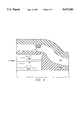
- FIG. 1 shows the Tiberio et al. setup in cross sectional elevation view.
- the output of a stripe heterojunction diode semiconductor laser typically operated in the lowest order TE mode, has a highly asymmetric near field pattern (see end on view of FIG. 2a) and a wide vertical spread angle (numerical aperture .sup. ⁇ 0.35, see elevation view of FIG. 2b) but a small horizontal spread (numerical aperture .sup. ⁇ 0.1) due to the typically large difference in index of refraction between the active core and the cladding and the small height to width ratio of the cavity.
- communication channel optical fibers which would carry the output of the semiconductor laser has a circular core (see end on view of FIG.
- FIG. 3a shows such a lens insertion to provide a high efficiency coupling
- FIG. 3b shows an optical fiber with its end rounded into a lens.
- wavelength division multiplexing requires combining outputs of discrete lasers using an optical fiber multiplexer which is bulky and costly.
- the present invention provides a semiconductor laser integrated with a silicon dioxide based waveguide having high efficiency coupling of the laser output into the waveguide by a integrated grating and a method of fabrication. This permits the laser output to be simply coupled into an optical fiber by a simple butt coupling of the optical fiber to the waveguide. Further, multiple lasers with different wavelengths can be integrated and their outputs coupled and combined into a single waveguide for wavelength division multiplexed operation.
- the present invention provides technical advantages including simple laser to optical fiber coupling, integrated circuit ruggedness of the laser plus waveguide, and simple compact wavelength division multiplex source structures.
- FIG. 1 shows in cross-sectional elevation view a known heterojunction diode semiconductor laser with distributed Bragg reflectors and wave launching grating.
- FIGS. 2a-d contrast output beam characteristics for semiconductor lasers and optical fibers.
- FIGS. 3a-b illustrate known lens systems for coupling semiconductor laser output into an optical fiber.
- FIGS. 4a-b are plan and cross sectional elevation views of a first preferred embodiment semiconductor laser and integrated dielectric waveguide.
- FIGS. 5a-b illustrate portions of FIG. 4b in greater detail.
- FIG. 6 is a band diagram.
- FIGS. 7a-f show steps in a preferred embodiment process of fabrication.
- FIG. 8 illustrates an alternative coupling grating
- FIGS. 4a-b show in simplified cross sectional elevation and plan views a first preferred embodiment structure, generally indicated by reference numeral 400, including semiconductor lasers 410, 420, 430, and 440 with outputs coupled to integrated phosphorus doped silicon dioxide (PSG) core waveguide 450 which has branches 451, 452, 453, and 454 of core 458 with each branch coupled to the output of one laser.
- Each laser has the structure of a heterojunction stripe diode with distributed Bragg reflectors at each end of the active layer; additionally, each laser also has a grating adjacent to the distributed Bragg reflector at one end for enhancing the vertical coupling of the laser output into the overlying branch of waveguide 450.
- an end portion of optical fiber 470 is shown butt-coupled to waveguide 450 with the core of optical fiber 470 aligned with the waveguide core 458.
- the preferred embodiment avoids the lens systems of FIGS. 3a-b.
- FIG. 4b shows a section through laser 410 and waveguide branch 451 and illustrates p type InGaAsP active area (which includes a four period multiple quantum well for carrier confinement and high efficiency) with p type InP anode 412 and n type InP cathode 413 on either side of the active area.
- Electrical current flowing through the diode causes electron-hole recombination in the active area (holes from anode 412 and electrons from cathode 413) which releases energy as photons.
- the InGaAsP layer forms the core of a semiconductor waveguide with the InP as the cladding.
- the semiconductor waveguide confines generated photons due to the index of refraction of the InGaAsP core being much greater than that of the InP cladding.
- Distributed Bragg reflectors 415 and 416 are formed as fingers (extending in the direction perpendicular to the plane of FIG. 4b) from the p type InP cladding. The period of these reflectors determines the lasing wavelength because reflection occurs when the period is a wavelength.
- FIGS. 4a-b show only a few fingers in each reflector for simplicity; each reflector typically has on the order of 1140 fingers.
- Grating 461 is adjacent reflector 416 and also has fingers formed in p+ type InP cladding and parallel to the fingers of reflectors 415-416. Take the period of grating 461 to provide highly efficient coupling of the laser output in the InGaAsP core waveguide into phosphorus doped silicon dioxide glass (PSG) core waveguide 450.
- PSG phosphorus doped silicon dioxide glass
- the broken arrow in FIG. 4b suggests the coupling.
- the longitudinal propagation constant (wave vector) in the InGaAsP core equals 2 ⁇ fn I /c where f is the output light frequency, n I is the effective index of refraction of the InGaAsP core at frequency f, and c is the speed of light in vacuum.
- the propagation constant in PSG core 458 is 2 ⁇ fn p /c with n p the effective index of refraction of the PSG core.
- the mechanical wave vector of the grating is 2 ⁇ /p.
- the coupling grating then provides the phase shift for high coupling efficiency.
- the period of grating 461 equals about 700 nm for infrared frequencies.
- Full coupling between, the semiconductor waveguide and the PSG waveguide occurs with a grating length of about 500 ⁇ m.
- Each of lasers 410, 420, 430, and 440 has a different frequency for lasing with the frequencies determined by the periods of the associated distributed Bragg reflectors.
- each waveguide branch, 451-454 feeds its associated laser's output into waveguide 450. This comprises wavelength division multiplexing.
- FIG. 5a is an enlarged view of a portion of FIG. 4b about the edge of anode 412 and shows metal anode contact 502, p+ InP anode 504, p InP anode 506, p InGaAsP active area 508, n InP cathode 510, n+ InP cathode 512, p InGaAsP waveguide core 528 with InP cladding by p+ InP 524, p InP 526, n InP 530, and n+ InP 532.
- the p InGaAsP layer forming active area 508 and semiconductor waveguide core 528 is a strained layer material system with quantum wells of InGaAs imbedded in InGaAsP barriers and sandwiched by 150 nm thick InGaAsP confinement layers.
- FIG. 6 shows a band diagram with the conduction and valence band edges.
- the bandgap of the InGaAs quantum wells is about 0.8 eV, so electron-hole recombination can release infrared light with free space wavelength about the common communication wavelength of 1.55 ⁇ m. Varying the quantum well thickness (between 2 and 12 nm) will move the quantized levels and thereby permit adjustment of the recombination energy.
- the bandgap of the adjoining InGaAsP is about 1.08 eV (corresponding to a free space wavelength of 1.15 ⁇ m) and the bandgap of the cladding InP is about 1.35 eV.
- the index of refraction of the InGaAsP (3.53) is higher than the index of refraction of the InP cladding (3.16), so the InGaAsP forms the core of a semiconductor waveguide. But the thickness of this core is comparable to or less than the wavelength of the generated light, so only a fraction (about 5% ) of the light energy is confined to the InGaAsP core and the light energy extends well into the InP cladding.
- the fingers 550 formed in p + InP 524 together with overlying silicon nitride 560 form a distributed Bragg reflector.
- the reflector acts on the light energy in the semiconductor waveguide and sets the lasing frequency as the frequency for total reflection.
- the frequency for total reflection simply is frequency at which the reflector fingers 550 have a period equal to a wavelength.
- the distributed Bragg reflectors have about 1140 fingers with a period of about 440 nm for light with a 1.55 ⁇ m free space wavelength.
- Each of the lasers 410, 420, 430, and 440 has the following dimensions: stripe width 5 ⁇ m (this also is roughly the width and height of the waveguide core 458 and the diameter of the core of butt-coupled optical fiber 470), length 500 ⁇ m, active area 508 and core 528 thickness about 0.4 ⁇ m, p InP anode 506 and cladding 526 thickness 1.75 ⁇ m, p+ InP cladding 524 thickness 1.5 ⁇ m with distributed Bragg reflector fingers 550 of height 0.05 ⁇ m, n InP cathode 510 and cladding 530 thickness 0.75 ⁇ m, and n+ InP cathode 512 and cladding 532 thickness 2 ⁇ m.
- the separation between adjacent lasers is about 250 ⁇ m, so there is no crosstalk despite the continuity of the cladding and core layers between the lasers.
- strained-layer quantum-well laser Alternative material systems may be used for the strained-layer quantum-well laser.
- strained material systems both compressive and tensile strain
- In x Ga 1-x As/InAs y P 1-y In x Ga 1-x As y P 1-y /InP
- Al x Ga y In 1-x-y As/InP for telecommunications (typically infrared from 0.9 to 1.55 ⁇ m free space wavelengths)
- AlGa(In)As(P)/GaAs for near infrared
- AlGaInP/GaAs for visible light.
- the In x Ga 1-x As/InAs y P 1-y bandgap and strain are directly correlated, both compressive and tensile strain.
- the In x Ga 1--x As y P 1--y /bandgap and strain can be adjusted independently (tensile strain only).
- the quantum well thickness is chosen to emit the desired wavelength light. For 1.55 ⁇ m, quantum well thickness varies from 3 to 10 nm depending upon whether the material is compressive strained to tensile strained and the amount of the strain.
- FIG. 5b is an enlarged view of a portion of FIG. 4b about the end of coupling grating 461 and shows p InGaAsP waveguide core 528, p InP cladding 526, p+ InP cladding 524, n InP cladding 530, n+ InP cladding 532 (all of these layers are extensions of the layers with same reference numerals as FIG. 5a), and grating fingers 555 of height 0.5 ⁇ m formed in p+ InP 524 with overlying silicon dioxide (“oxide") 570, PSG 572, and oxide 574.
- oxide silicon dioxide
- Coupling grating 461 has a total length of about 300 ⁇ m with a period of about 700 nm; thus coupling grating 461 has about 400 fingers.
- PSG 572 forms the core of a waveguide with oxide cladding 570 and 574.
- PSG core 572 has a diameter of about 5 ⁇ m and a roughly square cross sectional shape, and overlying oxide 574 has a thickness of about 6 ⁇ m.
- the thickness of oxide 570 directly between fingers 555 and PSG core 572 is about 0.3 ⁇ m, but this can be varied to optimize the coupling between the semiconductor waveguide with InGaAsP core 528 and the dielectric waveguide with PSG core 572.
- the longitudinal propagation constants in the semiconductor waveguide and the dielectric waveguide greatly differ. Indeed, for a 1.55 ⁇ m free space wavelength, the effective index of refraction of the semiconductor waveguide is about 3.545 and the effective index of refraction of the dielectric waveguide is about 1.4558. Thus coupling due to the interaction of closely spaced evanescent fields is negligible.
- coupling grating 461 provides the required phase matching between the semiconductor waveguide and the dielectric waveguide for high efficiency coupling.
- the periodicity of coupling grating 461 would be determined in the same manner.
- FIGS. 7a-h show in cross sectional elevation view steps of a preferred embodiment method of fabrication.
- GaAs buffer layer (1) Begin with a silicon substrate and grow a GaAs buffer layer, then grow the epitaxial layers as listed in following Table I; note that InGaAsP denotes In x Ga 1-x As y P 1-y for the barrier and spacer layers and InGaAs denotes In x Ga 1-x As for the quantum well layers.
- the GaAs buffer layer is grown at low temperature and provides compensation for the lattice mismatch between silicon and the other layers.
- each laser will have a different period in its reflector because four different wavelengths are being multiplexed, so use four separate lithography steps. However, the wavelengths of the four lasers will all be close to a free space wavelength of 1.55 ⁇ m.
- the areas away from the reflectors being defined are masked off and a thin layer of photoresist is applied and two laser sources are used to create the interference pattern for the exposure of the photoresist. Then the p+ InP layer is etch with the holographically patterned photoresist as mask to form the fingers of the reflectors. See FIG. 7 c .
- TEOS tetraethoxysilane
- PSG layer of thickness 5 ⁇ m by decomposition of TEOS with phosphine.
- photolithographically define the location of the PSG core of the dielectric waveguide and its branches, and etch away the PSG outside of the core.
- the core has a width of 5 ⁇ m and thus a cross section which is substantially square.
- an n+ type substrate could be used, and backside contact made to the cathode contact.
- the preferred embodiments may be varied in many ways while retaining one or more of the features of a coupling grating integrated between a semiconductor waveguide and a dielectric waveguide.
- the materials could be changed such as an InP substrate in place of the silicon substrate and GaAs buffer layer.
- the structure could be planarized by recessing the area on the wafer where the laser and coupling grating are formed, thus the dielectric waveguide would not go over a step.
- planarization could be accomplished by a planarization etch after the deposition of the first oxide layer and then another oxide layer deposited for the separation of the coupling grating from the dielectric waveguide core.
- Other dielectrics such as silicon nitride could be used in place of oxide and PSG in the dielectric waveguide.
- the coupling grating could be formed at the core-cladding interface of the dielectric waveguide.
- the evanescent wave from the InCaAsP core waveguide extends far enough into the oxide and PSG for such a grating to perform the necessary phase shift. But the grating may need to be fairly long, such as 300 ⁇ m. Forming this grating just amounts to doing the holographic lithography after the first oxide deposition rather than before it.
- FIG. 8 is analogous to FIG. 5b and shows such a grating.
- the doping types could be changed as long as a diode exists for recombination.
- the active area could be undoped or made without quantum wells or of more involved quantum well structure.
Abstract
Description
1/p=n.sub.I /λ-n.sub.p /λ
1/0.7≈3.545/1.55-1.4558/1.55
              TABLE I
______________________________________
Layer           Material     Thickness
______________________________________
Cladding        p + InP      5      μm
Cladding        p InP        1.75   μm
Spacer          p InGaAsP    150    nm
Quantum well    p InGaAs     8      nm
Barrier         p InGaAsP    10     nm
Quantum well    p InGaAs     8      nm
Barrier         p InGaAsP    10     nm
Quantum well    p InGaAs     8      nm
Barrier         p InGaAsP    10     nm
Quantum well    p InGaAs     8      nm
Barrier         p InGaAsP    10     nm
Quantum well    p InGaAs     8      nm
Spacer          p InGaAsP    150    nm
Cladding        n InP        0.75   μm
Cladding        n + InP      2      μm
Buffer          GaAs         15     μm
Substrate       Si           500    μm
______________________________________
Claims (21)
Priority Applications (1)
| Application Number | Priority Date | Filing Date | Title |
|---|---|---|---|
| US08/701,194 US5673284A (en) | 1994-05-25 | 1996-08-21 | Integrated laser and coupled waveguide |
Applications Claiming Priority (3)
| Application Number | Priority Date | Filing Date | Title |
|---|---|---|---|
| US08/248,937 US6064783A (en) | 1994-05-25 | 1994-05-25 | Integrated laser and coupled waveguide |
| US48585795A | 1995-06-07 | 1995-06-07 | |
| US08/701,194 US5673284A (en) | 1994-05-25 | 1996-08-21 | Integrated laser and coupled waveguide |
Related Parent Applications (1)
| Application Number | Title | Priority Date | Filing Date |
|---|---|---|---|
| US48585795A Continuation | 1994-05-25 | 1995-06-07 |
Publications (1)
| Publication Number | Publication Date |
|---|---|
| US5673284A true US5673284A (en) | 1997-09-30 |
Family
ID=22941341
Family Applications (2)
| Application Number | Title | Priority Date | Filing Date |
|---|---|---|---|
| US08/248,937 Expired - Lifetime US6064783A (en) | 1994-05-25 | 1994-05-25 | Integrated laser and coupled waveguide |
| US08/701,194 Expired - Lifetime US5673284A (en) | 1994-05-25 | 1996-08-21 | Integrated laser and coupled waveguide |
Family Applications Before (1)
| Application Number | Title | Priority Date | Filing Date |
|---|---|---|---|
| US08/248,937 Expired - Lifetime US6064783A (en) | 1994-05-25 | 1994-05-25 | Integrated laser and coupled waveguide |
Country Status (1)
| Country | Link |
|---|---|
| US (2) | US6064783A (en) |
Cited By (68)
| Publication number | Priority date | Publication date | Assignee | Title |
|---|---|---|---|---|
| WO2000003461A1 (en) * | 1998-07-10 | 2000-01-20 | Bookham Technology Plc | External cavity laser |
| WO2000036664A2 (en) * | 1998-12-17 | 2000-06-22 | Seiko Epson Corporation | Light-emitting device |
| WO2000073828A1 (en) * | 1999-06-01 | 2000-12-07 | Bookham Technology Plc | Waveguide junction with silicon nitride |
| US6158118A (en) * | 1999-03-31 | 2000-12-12 | International Business Machines Corporation | Method and apparatus for aligning surface mounted optoelectric semiconductor devices on a printed circuit board |
| US6185648B1 (en) | 1999-03-31 | 2001-02-06 | International Business Machines | Printer circuit board for an optoelectric computer system |
| US6229712B1 (en) | 1999-03-31 | 2001-05-08 | International Business Machines Corporation | Printed circuit board for coupling surface mounted optoelectric semiconductor devices |
| US6236773B1 (en) * | 1998-12-15 | 2001-05-22 | Texas Instruments Incorporated | Single wavelength semiconductor laser with grating-assisted dielectric waveguide coupler |
| WO2001039341A2 (en) * | 1999-10-22 | 2001-05-31 | Sarnoff Corporation | Integrated high power semiconductor laser with tapered active layer and co-directional grating |
| US6259840B1 (en) | 1999-03-31 | 2001-07-10 | International Business Machines Corporation | Printed circuit board having fluid-linked optical pathways for coupling surface mounted optoelectric semiconductor devices |
| US6282219B1 (en) * | 1998-08-12 | 2001-08-28 | Texas Instruments Incorporated | Substrate stack construction for enhanced coupling efficiency of optical couplers |
| US6327293B1 (en) * | 1998-08-12 | 2001-12-04 | Coherent, Inc. | Optically-pumped external-mirror vertical-cavity semiconductor-laser |
| WO2002011254A2 (en) * | 2000-07-31 | 2002-02-07 | Motorola, Inc. | Widely tunable laser structure |
| US6415070B1 (en) | 1999-03-31 | 2002-07-02 | International Business Machines Corporation | Method and apparatus for switching optical signals within an optoelectric computer network |
| US20020106160A1 (en) * | 2000-12-29 | 2002-08-08 | Honeywell International Inc. | Resonant reflector for increased wavelength and polarization control |
| US20020126942A1 (en) * | 2001-03-09 | 2002-09-12 | Photodigm, Inc. | Laterally coupled wave guides |
| US6529299B1 (en) | 1999-03-31 | 2003-03-04 | International Business Machines Corporation | Method and apparatus for broadcasting optical signals within an optoelectric computer network |
| US6600765B2 (en) | 2000-04-28 | 2003-07-29 | Photodigm, Inc. | High-power coherent arrays of vertical cavity surface-emitting semiconducting lasers |
| US20030161375A1 (en) * | 2001-07-24 | 2003-08-28 | Filgas David M. | Waveguide architecture, waveguide devices for laser processing and beam control, and laser processing applications |
| US6636547B2 (en) | 2000-04-28 | 2003-10-21 | Photodigm, Inc. | Multiple grating-outcoupled surface-emitting lasers |
| US6647048B2 (en) | 2000-04-28 | 2003-11-11 | Photodigm, Inc. | Grating-outcoupled surface-emitting lasers using quantum wells with thickness and composition variation |
| US6714575B2 (en) | 2001-03-05 | 2004-03-30 | Photodigm, Inc. | Optical modulator system |
| US6727646B1 (en) | 1999-03-23 | 2004-04-27 | Seiko Epson Corporation | Light-emitting device |
| US20040114642A1 (en) * | 2002-03-22 | 2004-06-17 | Bullington Jeff A. | Laser diode with output fiber feedback |
| US6782027B2 (en) * | 2000-12-29 | 2004-08-24 | Finisar Corporation | Resonant reflector for use with optoelectronic devices |
| US20040165637A1 (en) * | 2002-03-22 | 2004-08-26 | Bullington Jeff A. | Laser-to-fiber coupling |
| US20050025408A1 (en) * | 2003-08-01 | 2005-02-03 | Mclntyre Thomas J. | Method of forming interlayer connections in integrated optical circuits, and devices formed using same |
| US20050036533A1 (en) * | 2000-12-29 | 2005-02-17 | Honeywell To Finisar | Tunable detector |
| US20050078728A1 (en) * | 2003-10-09 | 2005-04-14 | Photodigm, Inc. | Chip-scale WDM system using grating-outcoupled surface-emitting lasers |
| US20050078727A1 (en) * | 2003-10-09 | 2005-04-14 | Photodigm, Inc. | Multi-wavelength grating-outcoupled surface emitting laser system |
| KR100472382B1 (en) * | 1997-12-05 | 2005-05-16 | 삼성전자주식회사 | Planar light-wave circuit module and manufacturing method therefor |
| US6963597B2 (en) | 2000-04-28 | 2005-11-08 | Photodigm, Inc. | Grating-outcoupled surface-emitting lasers |
| US6975664B1 (en) * | 1999-08-30 | 2005-12-13 | Agere Systems Inc. | Article comprising a two-dimensional photonic crystal coupler and method of making the same |
| US20070097680A1 (en) * | 2004-11-16 | 2007-05-03 | Canon Kabushiki Kaisha | Light-emitting photonic device |
| US20070127531A1 (en) * | 2005-12-07 | 2007-06-07 | Nl-Nanosemiconductor Gmbh | Laser source with broadband spectrum emission |
| FR2909491A1 (en) * | 2006-12-05 | 2008-06-06 | Commissariat Energie Atomique | Laser device for forming high speed optical link, has guiding structure with portion that delivers light generated by transmitting structure that is in III-V or in II-VI technology, where guiding structure is in silicon technology |
| US20080180674A1 (en) * | 2005-12-07 | 2008-07-31 | Innolume Gmbh | Optical Transmission System |
| US20090154871A1 (en) * | 2007-12-17 | 2009-06-18 | Electronics And Telecommunications Research Institute | Semiconductor integrated circuits including grating coupler for optical communication and methods of forming the same |
| US7555027B2 (en) | 2005-12-07 | 2009-06-30 | Innolume Gmbh | Laser source with broadband spectrum emission |
| US20090245298A1 (en) * | 2008-01-18 | 2009-10-01 | The Regents Of The University Of California | Hybrid silicon laser-quantum well intermixing wafer bonded integration platform for advanced photonic circuits with electroabsorption modulators |
| US20100142973A1 (en) * | 2005-12-07 | 2010-06-10 | Innolume Gmbh | Semiconductor laser with low relative intensity noise of individual longitudinal modes and optical transmission system incorporating the laser |
| US20110135252A1 (en) * | 2009-12-08 | 2011-06-09 | Electronics And Telecommunications Research Institute | Silicon photonics chip |
| US20120114003A1 (en) * | 2006-09-20 | 2012-05-10 | The Provost, Fellows And Scholars Of The College Of The Holy And | Laser device, a light signal generation device, and an optical resonator and a method for producing light |
| CN102621630A (en) * | 2001-10-30 | 2012-08-01 | Hoya美国公司 | Optical junction apparatus and methods employing optical power transverse-transfer |
| US20140376859A1 (en) * | 2011-07-12 | 2014-12-25 | Samsung Electronics Co., Ltd. | Multi-layer photoelectric integrated circuit device with overlapping devices |
| IT201700087052A1 (en) * | 2017-07-28 | 2019-01-28 | Prima Electro S P A | PROCEDURE FOR MANUFACTURING A LASER SEMICONDUCTOR DIODE, AND LASER DIODE |
| US20190204505A1 (en) * | 2017-12-30 | 2019-07-04 | Texas Instruments Incorporated | Additive photonic interconnects in microelectronic device |
| WO2020014154A1 (en) * | 2018-07-08 | 2020-01-16 | Artilux Inc. | Light emission apparatus |
| US10685994B2 (en) | 2015-08-04 | 2020-06-16 | Artilux, Inc. | Germanium-silicon light sensing apparatus |
| US10707260B2 (en) | 2015-08-04 | 2020-07-07 | Artilux, Inc. | Circuit for operating a multi-gate VIS/IR photodiode |
| US10739443B2 (en) | 2015-11-06 | 2020-08-11 | Artilux, Inc. | High-speed light sensing apparatus II |
| US10741598B2 (en) | 2015-11-06 | 2020-08-11 | Atrilux, Inc. | High-speed light sensing apparatus II |
| US10761599B2 (en) | 2015-08-04 | 2020-09-01 | Artilux, Inc. | Eye gesture tracking |
| US10770504B2 (en) | 2015-08-27 | 2020-09-08 | Artilux, Inc. | Wide spectrum optical sensor |
| US10777692B2 (en) | 2018-02-23 | 2020-09-15 | Artilux, Inc. | Photo-detecting apparatus and photo-detecting method thereof |
| US10795003B2 (en) | 2015-11-06 | 2020-10-06 | Artilux, Inc. | High-speed light sensing apparatus |
| US10854770B2 (en) | 2018-05-07 | 2020-12-01 | Artilux, Inc. | Avalanche photo-transistor |
| US10861888B2 (en) | 2015-08-04 | 2020-12-08 | Artilux, Inc. | Silicon germanium imager with photodiode in trench |
| US10886311B2 (en) | 2018-04-08 | 2021-01-05 | Artilux, Inc. | Photo-detecting apparatus |
| US10886312B2 (en) | 2015-11-06 | 2021-01-05 | Artilux, Inc. | High-speed light sensing apparatus II |
| US10969877B2 (en) | 2018-05-08 | 2021-04-06 | Artilux, Inc. | Display apparatus |
| US11262605B2 (en) * | 2017-08-31 | 2022-03-01 | Lightwave Logic Inc. | Active region-less polymer modulator integrated on a common PIC platform and method |
| US11335725B2 (en) | 2015-07-23 | 2022-05-17 | Artilux, Inc. | High efficiency wide spectrum sensor |
| JP7101437B1 (en) * | 2021-12-13 | 2022-07-15 | 株式会社京都セミコンダクター | Optical power converter |
| US11482553B2 (en) | 2018-02-23 | 2022-10-25 | Artilux, Inc. | Photo-detecting apparatus with subpixels |
| US11574942B2 (en) | 2018-12-12 | 2023-02-07 | Artilux, Inc. | Semiconductor device with low dark noise |
| US11630212B2 (en) | 2018-02-23 | 2023-04-18 | Artilux, Inc. | Light-sensing apparatus and light-sensing method thereof |
| US11637142B2 (en) | 2015-11-06 | 2023-04-25 | Artilux, Inc. | High-speed light sensing apparatus III |
| US11652184B2 (en) | 2019-08-28 | 2023-05-16 | Artilux, Inc. | Photo-detecting apparatus with low dark current |
Families Citing this family (35)
| Publication number | Priority date | Publication date | Assignee | Title |
|---|---|---|---|---|
| DE19826648B4 (en) * | 1998-06-16 | 2005-07-28 | Siemens Ag | Circuit carrier with an optical layer and optoelectronic component |
| US6389044B1 (en) | 1999-07-02 | 2002-05-14 | Corning Incorporated | Multi-wavelength laser usable for WDM applications and interferometric sensors |
| US6436613B1 (en) * | 1999-08-23 | 2002-08-20 | The Arizona Board Of Regents | Integrated hybrid optoelectronic devices |
| US6693033B2 (en) * | 2000-02-10 | 2004-02-17 | Motorola, Inc. | Method of removing an amorphous oxide from a monocrystalline surface |
| US6654533B1 (en) | 2000-06-16 | 2003-11-25 | Metrophotonics Inc. | Polarization independent waveguide structure |
| US6298186B1 (en) | 2000-07-07 | 2001-10-02 | Metrophotonics Inc. | Planar waveguide grating device and method having a passband with a flat-top and sharp-transitions |
| US20020096683A1 (en) * | 2001-01-19 | 2002-07-25 | Motorola, Inc. | Structure and method for fabricating GaN devices utilizing the formation of a compliant substrate |
| AUPR379001A0 (en) * | 2001-03-16 | 2001-04-12 | Redfern Integrated Optics Pty Ltd | Silica based monolithically integrated device and method |
| US20020192849A1 (en) * | 2001-03-22 | 2002-12-19 | Bullington Jeff A. | Low diode feedback |
| US6709989B2 (en) | 2001-06-21 | 2004-03-23 | Motorola, Inc. | Method for fabricating a semiconductor structure including a metal oxide interface with silicon |
| US7019332B2 (en) * | 2001-07-20 | 2006-03-28 | Freescale Semiconductor, Inc. | Fabrication of a wavelength locker within a semiconductor structure |
| US6693298B2 (en) | 2001-07-20 | 2004-02-17 | Motorola, Inc. | Structure and method for fabricating epitaxial semiconductor on insulator (SOI) structures and devices utilizing the formation of a compliant substrate for materials used to form same |
| US20030026310A1 (en) * | 2001-08-06 | 2003-02-06 | Motorola, Inc. | Structure and method for fabrication for a lighting device |
| US6639249B2 (en) * | 2001-08-06 | 2003-10-28 | Motorola, Inc. | Structure and method for fabrication for a solid-state lighting device |
| US6673667B2 (en) * | 2001-08-15 | 2004-01-06 | Motorola, Inc. | Method for manufacturing a substantially integral monolithic apparatus including a plurality of semiconductor materials |
| JP2003233925A (en) * | 2002-02-06 | 2003-08-22 | Pioneer Electronic Corp | Optical integrated device and wavelength variation cancellation method |
| US6771869B2 (en) * | 2002-04-18 | 2004-08-03 | Triquint Technology Holding Co. | Optoelectronic device having a barrier layer associated therewith and a method of manufacture thereof |
| US6917636B2 (en) * | 2002-08-22 | 2005-07-12 | Xponent Photonics Inc | Grating-stabilized semiconductor laser |
| US7169619B2 (en) * | 2002-11-19 | 2007-01-30 | Freescale Semiconductor, Inc. | Method for fabricating semiconductor structures on vicinal substrates using a low temperature, low pressure, alkaline earth metal-rich process |
| US6806202B2 (en) | 2002-12-03 | 2004-10-19 | Motorola, Inc. | Method of removing silicon oxide from a surface of a substrate |
| US6963090B2 (en) | 2003-01-09 | 2005-11-08 | Freescale Semiconductor, Inc. | Enhancement mode metal-oxide-semiconductor field effect transistor |
| US6985646B2 (en) * | 2003-01-24 | 2006-01-10 | Xponent Photonics Inc | Etched-facet semiconductor optical component with integrated end-coupled waveguide and methods of fabrication and use thereof |
| US7082147B2 (en) * | 2003-03-24 | 2006-07-25 | Eastman Kodak Company | Organic fiber laser system and method |
| US7643248B2 (en) * | 2006-06-30 | 2010-01-05 | Seagate Technology Llc | Optoelectronic emitter mounted on a slider |
| US7609480B2 (en) * | 2006-06-30 | 2009-10-27 | Seagate Technology Llc | Heat-assisted magnetic recording head |
| US8285149B2 (en) * | 2006-10-02 | 2012-10-09 | Futurewei Technologies, Inc. | Method and system for integrated DWDM transmitters |
| US8285150B2 (en) * | 2006-10-02 | 2012-10-09 | Futurewei Technologies, Inc. | Method and system for integrated DWDM transmitters |
| US8050525B2 (en) * | 2006-10-11 | 2011-11-01 | Futurewei Technologies, Inc. | Method and system for grating taps for monitoring a DWDM transmitter array integrated on a PLC platform |
| US8285151B2 (en) * | 2006-10-20 | 2012-10-09 | Futurewei Technologies, Inc. | Method and system for hybrid integrated 1XN DWDM transmitter |
| US8699837B2 (en) * | 2008-06-23 | 2014-04-15 | Imec | Method and system for coupling radiation |
| FR2947347B1 (en) * | 2009-06-26 | 2011-12-02 | Commissariat Energie Atomique | STRUCTURE AND METHOD FOR ALIGNING OPTICAL FIBER AND SUBMICRONIC WAVEGUIDE |
| US8577193B2 (en) | 2011-02-03 | 2013-11-05 | Seagate Technology Llc | Grating assisted surface emitter laser coupling for heat assisted magnetic recording |
| US8451695B2 (en) | 2011-06-23 | 2013-05-28 | Seagate Technology Llc | Vertical cavity surface emitting laser with integrated mirror and waveguide |
| US10545290B2 (en) | 2016-01-18 | 2020-01-28 | Corning Incorporated | Polymer clad fiber for evanescent coupling |
| US10514506B2 (en) | 2018-01-31 | 2019-12-24 | Corning Optical Communications LLC | Optical couplers for evanescent coupling of polymer clad fibers to optical waveguides using alignment features |
Citations (13)
| Publication number | Priority date | Publication date | Assignee | Title |
|---|---|---|---|---|
| US4097118A (en) * | 1975-10-30 | 1978-06-27 | Rca Corporation | Optical waveguide coupler employing deformed shape fiber-optic core coupling portion |
| US4286232A (en) * | 1978-06-09 | 1981-08-25 | Thomson-Csf | Laser with distributed reflector |
| US4318058A (en) * | 1979-04-24 | 1982-03-02 | Nippon Electric Co., Ltd. | Semiconductor diode laser array |
| US4747007A (en) * | 1984-09-17 | 1988-05-24 | Tdk Corporation | Spring means for biasing a tape against a head inserted in a cassette |
| JPH03263010A (en) * | 1990-03-14 | 1991-11-22 | Fujitsu Ltd | Fiber type bragg reflector |
| US5123070A (en) * | 1990-09-10 | 1992-06-16 | Tacan Corporation | Method of monolithic temperature-stabilization of a laser diode by evanescent coupling to a temperature stable grating |
| US5131060A (en) * | 1990-07-09 | 1992-07-14 | Canon Kabushiki Kaisha | Optical waveguide modulator communications device and method of modulating light using same |
| JPH04287389A (en) * | 1991-03-15 | 1992-10-12 | Nec Corp | Integrated type semiconductor laser element |
| US5220573A (en) * | 1989-03-10 | 1993-06-15 | Canon Kabushiki Kaisha | Optical apparatus using wavelength selective photocoupler |
| US5233187A (en) * | 1991-01-22 | 1993-08-03 | Canon Kabushiki Kaisha | Multi-wavelength light detecting and/or emitting apparatuses having serially arranged grating directional couplers |
| US5285508A (en) * | 1992-01-14 | 1994-02-08 | Pioneer Electronic Corporation | Optical wavelength converter |
| US5517589A (en) * | 1993-06-23 | 1996-05-14 | Canon Kabushiki Kaisha | Optical wavelength multiplexing and demultiplexing device for multiplexing or demultiplexing light having a plurality of modes and photodetector using the same |
| US5528616A (en) * | 1995-04-24 | 1996-06-18 | International Business Machines Corporation | Asymmetric dual waveguide laser |
Family Cites Families (3)
| Publication number | Priority date | Publication date | Assignee | Title |
|---|---|---|---|---|
| GB1535171A (en) * | 1975-12-04 | 1978-12-06 | Nat Res Dev | Optical waveguide coupling arrangements |
| US4737007A (en) * | 1986-02-24 | 1988-04-12 | American Telephone And Telegraph Company, At&T Bell Laboratories | Narrow-band wavelength selective optical coupler |
| US5070488A (en) * | 1988-06-29 | 1991-12-03 | Atsuko Fukushima | Optical integrated circuit and optical apparatus |
-
1994
- 1994-05-25 US US08/248,937 patent/US6064783A/en not_active Expired - Lifetime
-
1996
- 1996-08-21 US US08/701,194 patent/US5673284A/en not_active Expired - Lifetime
Patent Citations (13)
| Publication number | Priority date | Publication date | Assignee | Title |
|---|---|---|---|---|
| US4097118A (en) * | 1975-10-30 | 1978-06-27 | Rca Corporation | Optical waveguide coupler employing deformed shape fiber-optic core coupling portion |
| US4286232A (en) * | 1978-06-09 | 1981-08-25 | Thomson-Csf | Laser with distributed reflector |
| US4318058A (en) * | 1979-04-24 | 1982-03-02 | Nippon Electric Co., Ltd. | Semiconductor diode laser array |
| US4747007A (en) * | 1984-09-17 | 1988-05-24 | Tdk Corporation | Spring means for biasing a tape against a head inserted in a cassette |
| US5220573A (en) * | 1989-03-10 | 1993-06-15 | Canon Kabushiki Kaisha | Optical apparatus using wavelength selective photocoupler |
| JPH03263010A (en) * | 1990-03-14 | 1991-11-22 | Fujitsu Ltd | Fiber type bragg reflector |
| US5131060A (en) * | 1990-07-09 | 1992-07-14 | Canon Kabushiki Kaisha | Optical waveguide modulator communications device and method of modulating light using same |
| US5123070A (en) * | 1990-09-10 | 1992-06-16 | Tacan Corporation | Method of monolithic temperature-stabilization of a laser diode by evanescent coupling to a temperature stable grating |
| US5233187A (en) * | 1991-01-22 | 1993-08-03 | Canon Kabushiki Kaisha | Multi-wavelength light detecting and/or emitting apparatuses having serially arranged grating directional couplers |
| JPH04287389A (en) * | 1991-03-15 | 1992-10-12 | Nec Corp | Integrated type semiconductor laser element |
| US5285508A (en) * | 1992-01-14 | 1994-02-08 | Pioneer Electronic Corporation | Optical wavelength converter |
| US5517589A (en) * | 1993-06-23 | 1996-05-14 | Canon Kabushiki Kaisha | Optical wavelength multiplexing and demultiplexing device for multiplexing or demultiplexing light having a plurality of modes and photodetector using the same |
| US5528616A (en) * | 1995-04-24 | 1996-06-18 | International Business Machines Corporation | Asymmetric dual waveguide laser |
Non-Patent Citations (2)
| Title |
|---|
| Aiki et al, "A Frequency-Multiplexing Light Source with Monolithically Integrated Distributed Feedback Diode Lasers", IEEE Journal of Quantum Electronics, vol. QE-13, No. 4, Apr. 1977, pp. 220-223. |
| Aiki et al, A Frequency Multiplexing Light Source with Monolithically Integrated Distributed Feedback Diode Lasers , IEEE Journal of Quantum Electronics, vol. QE 13, No. 4, Apr. 1977, pp. 220 223. * |
Cited By (112)
| Publication number | Priority date | Publication date | Assignee | Title |
|---|---|---|---|---|
| KR100472382B1 (en) * | 1997-12-05 | 2005-05-16 | 삼성전자주식회사 | Planar light-wave circuit module and manufacturing method therefor |
| US6487328B2 (en) | 1997-12-15 | 2002-11-26 | Texas Instruments Incorporated | Single wavelength semiconductor laser with grating-assisted dielectric waveguide coupler |
| WO2000003461A1 (en) * | 1998-07-10 | 2000-01-20 | Bookham Technology Plc | External cavity laser |
| US6282219B1 (en) * | 1998-08-12 | 2001-08-28 | Texas Instruments Incorporated | Substrate stack construction for enhanced coupling efficiency of optical couplers |
| US6327293B1 (en) * | 1998-08-12 | 2001-12-04 | Coherent, Inc. | Optically-pumped external-mirror vertical-cavity semiconductor-laser |
| US6236773B1 (en) * | 1998-12-15 | 2001-05-22 | Texas Instruments Incorporated | Single wavelength semiconductor laser with grating-assisted dielectric waveguide coupler |
| WO2000036664A2 (en) * | 1998-12-17 | 2000-06-22 | Seiko Epson Corporation | Light-emitting device |
| WO2000036664A3 (en) * | 1998-12-17 | 2000-11-16 | Seiko Epson Corp | Light-emitting device |
| US6704335B1 (en) | 1998-12-17 | 2004-03-09 | Seiko Epson Corporation | Light-emitting device |
| US6727646B1 (en) | 1999-03-23 | 2004-04-27 | Seiko Epson Corporation | Light-emitting device |
| US6259840B1 (en) | 1999-03-31 | 2001-07-10 | International Business Machines Corporation | Printed circuit board having fluid-linked optical pathways for coupling surface mounted optoelectric semiconductor devices |
| US6229712B1 (en) | 1999-03-31 | 2001-05-08 | International Business Machines Corporation | Printed circuit board for coupling surface mounted optoelectric semiconductor devices |
| US6529299B1 (en) | 1999-03-31 | 2003-03-04 | International Business Machines Corporation | Method and apparatus for broadcasting optical signals within an optoelectric computer network |
| US6415070B1 (en) | 1999-03-31 | 2002-07-02 | International Business Machines Corporation | Method and apparatus for switching optical signals within an optoelectric computer network |
| US6185648B1 (en) | 1999-03-31 | 2001-02-06 | International Business Machines | Printer circuit board for an optoelectric computer system |
| US6158118A (en) * | 1999-03-31 | 2000-12-12 | International Business Machines Corporation | Method and apparatus for aligning surface mounted optoelectric semiconductor devices on a printed circuit board |
| WO2000073828A1 (en) * | 1999-06-01 | 2000-12-07 | Bookham Technology Plc | Waveguide junction with silicon nitride |
| US6975664B1 (en) * | 1999-08-30 | 2005-12-13 | Agere Systems Inc. | Article comprising a two-dimensional photonic crystal coupler and method of making the same |
| WO2001039341A3 (en) * | 1999-10-22 | 2002-08-01 | Sarnoff Corp | Integrated high power semiconductor laser with tapered active layer and co-directional grating |
| US6829276B1 (en) | 1999-10-22 | 2004-12-07 | Trumpf Photonics, Inc. | Integrated high power semiconductor laser |
| WO2001039341A2 (en) * | 1999-10-22 | 2001-05-31 | Sarnoff Corporation | Integrated high power semiconductor laser with tapered active layer and co-directional grating |
| US6600765B2 (en) | 2000-04-28 | 2003-07-29 | Photodigm, Inc. | High-power coherent arrays of vertical cavity surface-emitting semiconducting lasers |
| US20060056479A1 (en) * | 2000-04-28 | 2006-03-16 | Photodigm | Grating--outcoupled surface-emitting lasers |
| US6636547B2 (en) | 2000-04-28 | 2003-10-21 | Photodigm, Inc. | Multiple grating-outcoupled surface-emitting lasers |
| US6647048B2 (en) | 2000-04-28 | 2003-11-11 | Photodigm, Inc. | Grating-outcoupled surface-emitting lasers using quantum wells with thickness and composition variation |
| US7450624B2 (en) | 2000-04-28 | 2008-11-11 | Photodigm, Inc. | Grating—outcoupled surface-emitting lasers |
| US6963597B2 (en) | 2000-04-28 | 2005-11-08 | Photodigm, Inc. | Grating-outcoupled surface-emitting lasers |
| WO2002011254A3 (en) * | 2000-07-31 | 2003-07-31 | Motorola Inc | Widely tunable laser structure |
| WO2002011254A2 (en) * | 2000-07-31 | 2002-02-07 | Motorola, Inc. | Widely tunable laser structure |
| US6836501B2 (en) * | 2000-12-29 | 2004-12-28 | Finisar Corporation | Resonant reflector for increased wavelength and polarization control |
| US20050036533A1 (en) * | 2000-12-29 | 2005-02-17 | Honeywell To Finisar | Tunable detector |
| US6782027B2 (en) * | 2000-12-29 | 2004-08-24 | Finisar Corporation | Resonant reflector for use with optoelectronic devices |
| US8599897B2 (en) | 2000-12-29 | 2013-12-03 | Finisar Corporation | Tunable detector |
| US20020106160A1 (en) * | 2000-12-29 | 2002-08-08 | Honeywell International Inc. | Resonant reflector for increased wavelength and polarization control |
| US6714575B2 (en) | 2001-03-05 | 2004-03-30 | Photodigm, Inc. | Optical modulator system |
| US6775427B2 (en) * | 2001-03-09 | 2004-08-10 | Photodigm, Inc. | Laterally coupled wave guides |
| US20020126942A1 (en) * | 2001-03-09 | 2002-09-12 | Photodigm, Inc. | Laterally coupled wave guides |
| US20030161375A1 (en) * | 2001-07-24 | 2003-08-28 | Filgas David M. | Waveguide architecture, waveguide devices for laser processing and beam control, and laser processing applications |
| US7065121B2 (en) * | 2001-07-24 | 2006-06-20 | Gsi Group Ltd. | Waveguide architecture, waveguide devices for laser processing and beam control, and laser processing applications |
| CN102621630B (en) * | 2001-10-30 | 2015-03-25 | Hoya美国公司 | Optical junction apparatus and methods employing optical power transverse-transfer |
| CN102621630A (en) * | 2001-10-30 | 2012-08-01 | Hoya美国公司 | Optical junction apparatus and methods employing optical power transverse-transfer |
| US20040114642A1 (en) * | 2002-03-22 | 2004-06-17 | Bullington Jeff A. | Laser diode with output fiber feedback |
| US7194016B2 (en) * | 2002-03-22 | 2007-03-20 | The Research Foundation Of The University Of Central Florida | Laser-to-fiber coupling |
| US20040165637A1 (en) * | 2002-03-22 | 2004-08-26 | Bullington Jeff A. | Laser-to-fiber coupling |
| US7206480B2 (en) * | 2003-08-01 | 2007-04-17 | Bae Systems Information And Electronic Systems Integration Inc. | Method of forming interlayer connections in integrated optical circuits, and devices formed using same |
| US20050025408A1 (en) * | 2003-08-01 | 2005-02-03 | Mclntyre Thomas J. | Method of forming interlayer connections in integrated optical circuits, and devices formed using same |
| US7113526B2 (en) | 2003-10-09 | 2006-09-26 | Photodigm, Inc. | Multi-wavelength grating-outcoupled surface emitting laser system |
| US7092598B2 (en) | 2003-10-09 | 2006-08-15 | Photodigm, Inc. | Chip-scale WDM system using grating-outcoupled surface-emitting lasers |
| US20050078727A1 (en) * | 2003-10-09 | 2005-04-14 | Photodigm, Inc. | Multi-wavelength grating-outcoupled surface emitting laser system |
| US20050078728A1 (en) * | 2003-10-09 | 2005-04-14 | Photodigm, Inc. | Chip-scale WDM system using grating-outcoupled surface-emitting lasers |
| US20070097680A1 (en) * | 2004-11-16 | 2007-05-03 | Canon Kabushiki Kaisha | Light-emitting photonic device |
| US7772606B2 (en) | 2004-11-16 | 2010-08-10 | Canon Kabushiki Kaisha | Light-emitting photonic device |
| US20100142973A1 (en) * | 2005-12-07 | 2010-06-10 | Innolume Gmbh | Semiconductor laser with low relative intensity noise of individual longitudinal modes and optical transmission system incorporating the laser |
| US7555027B2 (en) | 2005-12-07 | 2009-06-30 | Innolume Gmbh | Laser source with broadband spectrum emission |
| US7561607B2 (en) * | 2005-12-07 | 2009-07-14 | Innolume Gmbh | Laser source with broadband spectrum emission |
| US20080180674A1 (en) * | 2005-12-07 | 2008-07-31 | Innolume Gmbh | Optical Transmission System |
| US7835408B2 (en) | 2005-12-07 | 2010-11-16 | Innolume Gmbh | Optical transmission system |
| US20070127531A1 (en) * | 2005-12-07 | 2007-06-07 | Nl-Nanosemiconductor Gmbh | Laser source with broadband spectrum emission |
| US8411711B2 (en) | 2005-12-07 | 2013-04-02 | Innolume Gmbh | Semiconductor laser with low relative intensity noise of individual longitudinal modes and optical transmission system incorporating the laser |
| US20120114003A1 (en) * | 2006-09-20 | 2012-05-10 | The Provost, Fellows And Scholars Of The College Of The Holy And | Laser device, a light signal generation device, and an optical resonator and a method for producing light |
| US8971371B2 (en) * | 2006-12-05 | 2015-03-03 | Commissariat A L'energie Atomique | Laser device with coupled laser source and waveguide |
| FR2909491A1 (en) * | 2006-12-05 | 2008-06-06 | Commissariat Energie Atomique | Laser device for forming high speed optical link, has guiding structure with portion that delivers light generated by transmitting structure that is in III-V or in II-VI technology, where guiding structure is in silicon technology |
| US20100142580A1 (en) * | 2006-12-05 | 2010-06-10 | Commissariat A L'energie Atomique | Laser device with coupled laser source and waveguide |
| WO2008068209A1 (en) * | 2006-12-05 | 2008-06-12 | Commissariat A L'energie Atomique | Laser device with coupled laser source and waveguide |
| US20100111469A1 (en) * | 2007-12-17 | 2010-05-06 | Electronics And Telecommunications Research Institute | Semiconductor integrated circuits including grating coupler for optical communication and methods of forming the same |
| US20090154871A1 (en) * | 2007-12-17 | 2009-06-18 | Electronics And Telecommunications Research Institute | Semiconductor integrated circuits including grating coupler for optical communication and methods of forming the same |
| US8165437B2 (en) * | 2007-12-17 | 2012-04-24 | Electronics And Telecommunications Research Institute | Semiconductor integrated circuits including grating coupler for optical communication and methods of forming the same |
| CN103259185A (en) * | 2008-01-18 | 2013-08-21 | 加利福尼亚大学董事会 | Hybrid silicon laser-quantum well intermixing wafer bonded integration platform |
| US8559478B2 (en) * | 2008-01-18 | 2013-10-15 | The Regents Of The University Of California | Hybrid silicon laser-quantum well intermixing wafer bonded integration platform for advanced photonic circuits with electroabsorption modulators |
| US20090245298A1 (en) * | 2008-01-18 | 2009-10-01 | The Regents Of The University Of California | Hybrid silicon laser-quantum well intermixing wafer bonded integration platform for advanced photonic circuits with electroabsorption modulators |
| CN103259185B (en) * | 2008-01-18 | 2016-05-04 | 加利福尼亚大学董事会 | The integrated platform of silicon laser instrument-SQW hybrid chip combination |
| US20110135252A1 (en) * | 2009-12-08 | 2011-06-09 | Electronics And Telecommunications Research Institute | Silicon photonics chip |
| US20140376859A1 (en) * | 2011-07-12 | 2014-12-25 | Samsung Electronics Co., Ltd. | Multi-layer photoelectric integrated circuit device with overlapping devices |
| US11335725B2 (en) | 2015-07-23 | 2022-05-17 | Artilux, Inc. | High efficiency wide spectrum sensor |
| US10964742B2 (en) | 2015-08-04 | 2021-03-30 | Artilux, Inc. | Germanium-silicon light sensing apparatus II |
| US10861888B2 (en) | 2015-08-04 | 2020-12-08 | Artilux, Inc. | Silicon germanium imager with photodiode in trench |
| US10761599B2 (en) | 2015-08-04 | 2020-09-01 | Artilux, Inc. | Eye gesture tracking |
| US11755104B2 (en) | 2015-08-04 | 2023-09-12 | Artilux, Inc. | Eye gesture tracking |
| US10685994B2 (en) | 2015-08-04 | 2020-06-16 | Artilux, Inc. | Germanium-silicon light sensing apparatus |
| US10707260B2 (en) | 2015-08-04 | 2020-07-07 | Artilux, Inc. | Circuit for operating a multi-gate VIS/IR photodiode |
| US11756969B2 (en) | 2015-08-04 | 2023-09-12 | Artilux, Inc. | Germanium-silicon light sensing apparatus |
| US10756127B2 (en) | 2015-08-04 | 2020-08-25 | Artilux, Inc. | Germanium-silicon light sensing apparatus |
| US10770504B2 (en) | 2015-08-27 | 2020-09-08 | Artilux, Inc. | Wide spectrum optical sensor |
| US11747450B2 (en) | 2015-11-06 | 2023-09-05 | Artilux, Inc. | High-speed light sensing apparatus |
| US10886312B2 (en) | 2015-11-06 | 2021-01-05 | Artilux, Inc. | High-speed light sensing apparatus II |
| US10739443B2 (en) | 2015-11-06 | 2020-08-11 | Artilux, Inc. | High-speed light sensing apparatus II |
| US10795003B2 (en) | 2015-11-06 | 2020-10-06 | Artilux, Inc. | High-speed light sensing apparatus |
| US11749696B2 (en) | 2015-11-06 | 2023-09-05 | Artilux, Inc. | High-speed light sensing apparatus II |
| US11579267B2 (en) | 2015-11-06 | 2023-02-14 | Artilux, Inc. | High-speed light sensing apparatus |
| US11131757B2 (en) | 2015-11-06 | 2021-09-28 | Artilux, Inc. | High-speed light sensing apparatus |
| US10741598B2 (en) | 2015-11-06 | 2020-08-11 | Atrilux, Inc. | High-speed light sensing apparatus II |
| US10886309B2 (en) | 2015-11-06 | 2021-01-05 | Artilux, Inc. | High-speed light sensing apparatus II |
| US11637142B2 (en) | 2015-11-06 | 2023-04-25 | Artilux, Inc. | High-speed light sensing apparatus III |
| IT201700087052A1 (en) * | 2017-07-28 | 2019-01-28 | Prima Electro S P A | PROCEDURE FOR MANUFACTURING A LASER SEMICONDUCTOR DIODE, AND LASER DIODE |
| US10958041B2 (en) * | 2017-07-28 | 2021-03-23 | Prima Electro S.P.A. | Method for making a semiconductor laser diode, and laser diode |
| EP3435499A1 (en) * | 2017-07-28 | 2019-01-30 | Prima Electro S.p.A. | Method for making a semiconductor laser diode, and laser diode |
| US20190036306A1 (en) * | 2017-07-28 | 2019-01-31 | Prima Electro S.P.A | Method for Making a Semiconductor Laser Diode, and Laser Diode |
| US11262605B2 (en) * | 2017-08-31 | 2022-03-01 | Lightwave Logic Inc. | Active region-less polymer modulator integrated on a common PIC platform and method |
| US20190204505A1 (en) * | 2017-12-30 | 2019-07-04 | Texas Instruments Incorporated | Additive photonic interconnects in microelectronic device |
| US11482553B2 (en) | 2018-02-23 | 2022-10-25 | Artilux, Inc. | Photo-detecting apparatus with subpixels |
| US10777692B2 (en) | 2018-02-23 | 2020-09-15 | Artilux, Inc. | Photo-detecting apparatus and photo-detecting method thereof |
| US11630212B2 (en) | 2018-02-23 | 2023-04-18 | Artilux, Inc. | Light-sensing apparatus and light-sensing method thereof |
| US10886311B2 (en) | 2018-04-08 | 2021-01-05 | Artilux, Inc. | Photo-detecting apparatus |
| US11329081B2 (en) | 2018-04-08 | 2022-05-10 | Artilux, Inc. | Photo-detecting apparatus |
| US10854770B2 (en) | 2018-05-07 | 2020-12-01 | Artilux, Inc. | Avalanche photo-transistor |
| US10969877B2 (en) | 2018-05-08 | 2021-04-06 | Artilux, Inc. | Display apparatus |
| WO2020014154A1 (en) * | 2018-07-08 | 2020-01-16 | Artilux Inc. | Light emission apparatus |
| US11574942B2 (en) | 2018-12-12 | 2023-02-07 | Artilux, Inc. | Semiconductor device with low dark noise |
| US11652184B2 (en) | 2019-08-28 | 2023-05-16 | Artilux, Inc. | Photo-detecting apparatus with low dark current |
| US11777049B2 (en) | 2019-08-28 | 2023-10-03 | Artilux, Inc. | Photo-detecting apparatus with low dark current |
| WO2023112090A1 (en) * | 2021-12-13 | 2023-06-22 | 株式会社京都セミコンダクター | Optical power supply converter |
| JP7101437B1 (en) * | 2021-12-13 | 2022-07-15 | 株式会社京都セミコンダクター | Optical power converter |
Also Published As
| Publication number | Publication date |
|---|---|
| US6064783A (en) | 2000-05-16 |
Similar Documents
| Publication | Publication Date | Title |
|---|---|---|
| US5673284A (en) | Integrated laser and coupled waveguide | |
| US6282219B1 (en) | Substrate stack construction for enhanced coupling efficiency of optical couplers | |
| EP1368870B1 (en) | Asymmetric waveguide electroabsorption-modulated laser | |
| US6681069B2 (en) | Semiconductor optical component utilizing leaky structures to match the mode of rib waveguides to that of the fiber | |
| CN102378933A (en) | Narrow surface corrugated grating | |
| US5838854A (en) | Integrated optical control element and a method for fabricating the same and optical integrated circuit element and optical integrated circuit device using the same | |
| US20060176544A1 (en) | Folded cavity semiconductor optical amplifier (FCSOA) | |
| US6282345B1 (en) | Device for coupling waveguides to one another | |
| US6400864B1 (en) | Broad band semiconductor optical amplifier module having optical amplifiers for amplifying demutiplexed signals of different wavelengths and optical communication system using it | |
| Menezo et al. | 10-wavelength 200-GHz channel spacing emitter integrating DBR lasers with a PHASAR on InP for WDM applications | |
| CN111740311B (en) | Narrow linewidth tunable laser and preparation method thereof | |
| JP2003258368A (en) | Semiconductor optical element | |
| US5606573A (en) | Method and apparatus for control of lasing wavelength in distributed feedback lasers | |
| US5239600A (en) | Optical device with an optical coupler for effecting light branching/combining by splitting a wavefront of light | |
| JP3284994B2 (en) | Semiconductor optical integrated device and method of manufacturing the same | |
| JP3336994B2 (en) | Method of manufacturing semiconductor optical waveguide array and semiconductor optical device having array structure | |
| US6937633B2 (en) | Multi-wavelength semiconductor lasers | |
| JP2907234B2 (en) | Semiconductor wavelength tunable device | |
| JP2001185805A (en) | Optical semiconductor device | |
| JPH08292336A (en) | Production of optical semiconductor integrated circuit | |
| Lammert et al. | Dual-channel strained-layer in GaAs-GaAs-AlGaAs WDM source with integrated coupler by selective-area MOCVD | |
| WO2023105759A1 (en) | Wavelength-multiplexing light source | |
| JPH06268316A (en) | Semiconductor optical element | |
| Zah et al. | Multiwavelength light source with integrated DFB laser array and star coupler for WDM lightwave communications | |
| JP2953368B2 (en) | Optical semiconductor integrated circuit |
Legal Events
| Date | Code | Title | Description |
|---|---|---|---|
| STCF | Information on status: patent grant |
Free format text: PATENTED CASE |
|
| FPAY | Fee payment |
Year of fee payment: 4 |
|
| AS | Assignment |
Owner name: PHOTODIGM, INC., TEXAS Free format text: ASSIGNMENT OF ASSIGNORS INTEREST;ASSIGNOR:EVANS, GARY A.;REEL/FRAME:012607/0824 Effective date: 20020103 |
|
| AS | Assignment |
Owner name: SILICON VALLEY BANK, CALIFORNIA Free format text: SECURITY INTEREST;ASSIGNOR:PHOTODIGM, INC.;REEL/FRAME:013011/0641 Effective date: 20020606 |
|
| AS | Assignment |
Owner name: AMT CAPITAL, LTD., TEXAS Free format text: SECURITY AGREEMENT;ASSIGNOR:PHOTODIGM, INC.;REEL/FRAME:015653/0654 Effective date: 20030626 |
|
| FPAY | Fee payment |
Year of fee payment: 8 |
|
| FPAY | Fee payment |
Year of fee payment: 12 |
|
| AS | Assignment |
Owner name: ANTHONY J. LEVECCHIO, AGENT, TEXAS Free format text: SECURITY AGREEMENT;ASSIGNOR:PHOTODIGM, INC.;REEL/FRAME:022529/0062 Effective date: 20081205 |
|
| AS | Assignment |
Owner name: PHOTODIGM INC, TEXAS Free format text: RELEASE;ASSIGNOR:SILICON VALLEY BANK;REEL/FRAME:023708/0340 Effective date: 20091222 |
|
| FEPP | Fee payment procedure |
Free format text: PAYOR NUMBER ASSIGNED (ORIGINAL EVENT CODE: ASPN); ENTITY STATUS OF PATENT OWNER: LARGE ENTITY |
|
| AS | Assignment |
Owner name: PHOTODIGM, INC., TEXAS Free format text: RELEASE;ASSIGNOR:SILICON VALLEY BANK;REEL/FRAME:027495/0521 Effective date: 20111220 |
|
| AS | Assignment |
Owner name: KELTON CAPITAL, L.L.C., DELAWARE Free format text: ASSIGNMENT OF ASSIGNORS INTEREST;ASSIGNOR:PHOTODIGM, INC.;REEL/FRAME:028045/0546 Effective date: 20120229 |
|
| AS | Assignment |
Owner name: TEXAS INSTRUMENTS INCORPORATED, TEXAS Free format text: ASSIGNMENT OF ASSIGNORS INTEREST;ASSIGNORS:CONGDON, PHILIP A.;PANG, LILY Y.;REEL/FRAME:028659/0345 Effective date: 19940811 |
|
| AS | Assignment |
Owner name: PHOTODIGM, INC., TEXAS Free format text: RELEASE BY SECURED PARTY;ASSIGNOR:ANTHONY J. LEVECCHIO;REEL/FRAME:028838/0487 Effective date: 20111216 Owner name: PHOTODIGM, INC., TEXAS Free format text: RELEASE BY SECURED PARTY;ASSIGNOR:AMT CAPITAL, LTD.;REEL/FRAME:028838/0013 Effective date: 20111216 |
|
| AS | Assignment |
Owner name: HANGER SOLUTIONS, LLC, GEORGIA Free format text: ASSIGNMENT OF ASSIGNORS INTEREST;ASSIGNOR:INTELLECTUAL VENTURES ASSETS 158 LLC;REEL/FRAME:051486/0425 Effective date: 20191206 |
|
| AS | Assignment |
Owner name: INTELLECTUAL VENTURES ASSETS 158 LLC, DELAWARE Free format text: ASSIGNMENT OF ASSIGNORS INTEREST;ASSIGNOR:CHEMTRON RESEARCH LLC;REEL/FRAME:051754/0027 Effective date: 20191126 |
|
| AS | Assignment |
Owner name: INTELLECTUAL VENTURES ASSETS 158 LLC, DELAWARE Free format text: ASSIGNMENT OF ASSIGNORS INTEREST;ASSIGNOR:CHEMTRON RESEARCH LLC;REEL/FRAME:051776/0952 Effective date: 20191126 |