US5650996A - Method and circuit arrangement for combining several digital data channels on a transmission channel - Google Patents
Method and circuit arrangement for combining several digital data channels on a transmission channel Download PDFInfo
- Publication number
- US5650996A US5650996A US08/456,410 US45641095A US5650996A US 5650996 A US5650996 A US 5650996A US 45641095 A US45641095 A US 45641095A US 5650996 A US5650996 A US 5650996A
- Authority
- US
- United States
- Prior art keywords
- data
- signal
- modulated
- frequency
- circuit arrangement
- Prior art date
- Legal status (The legal status is an assumption and is not a legal conclusion. Google has not performed a legal analysis and makes no representation as to the accuracy of the status listed.)
- Expired - Lifetime
Links
- 238000000034 method Methods 0.000 title claims abstract description 38
- 230000005540 biological transmission Effects 0.000 title claims abstract description 29
- 230000001360 synchronised effect Effects 0.000 claims description 3
- 238000010586 diagram Methods 0.000 description 7
- 230000015572 biosynthetic process Effects 0.000 description 1
- 238000010295 mobile communication Methods 0.000 description 1
- 238000000926 separation method Methods 0.000 description 1
- 230000008054 signal transmission Effects 0.000 description 1
Images


Classifications
-
- G—PHYSICS
- G08—SIGNALLING
- G08C—TRANSMISSION SYSTEMS FOR MEASURED VALUES, CONTROL OR SIMILAR SIGNALS
- G08C15/00—Arrangements characterised by the use of multiplexing for the transmission of a plurality of signals over a common path
- G08C15/02—Arrangements characterised by the use of multiplexing for the transmission of a plurality of signals over a common path simultaneously, i.e. using frequency division
- G08C15/04—Arrangements characterised by the use of multiplexing for the transmission of a plurality of signals over a common path simultaneously, i.e. using frequency division the signals being modulated on carrier frequencies
Definitions
- the present invention relates to a method and a circuit arrangement for combining several digital data channels having different data rates, on a common transmission channel of a transmitter.
- Transmitting data signals on a data channel with a certain frequency is known.
- an additional transmission channel having a different frequency from the first transmission channel is needed.
- an electronic search circuit is employed to seek an available one of a plurality of transmission channels through which the desired data signal can still be transmitted.
- Such electronic search circuits are relatively complex.
- whether or not a free transmission channel can be found is a matter of chance.
- the present invention provides a method, and a circuit arrangement implementing the method, which fulfill the above need.
- several data signals can be combined into a single transmission channel, thereby permitting the data signals to be transmitted essentially at the same time.
- fewer transmission channels are needed, which in turn increases transmission capacity.
- the data signals to be transmitted can be advantageously evaluated independent of one another, to a significant extent at the receiver.
- the modulation of the data channels is not restricted, thereby permitting the carrier frequency of the data signal to be amplitude-modulated or frequency-modulated.
- the time of the data signals can be synchronized with a simple cycle signal, thereby permitting a clear assignment of the signals when the signals are decoded at the receiver.
- the period of the additional data signal to be transmitted is a multiple of the period duration of the first data signal, thereby permitting easy signal separation and causing little signal loss.
- the further data signal is modulated in the half bit period pursuant to the biphase/Manchester method. Since the signal becomes zero in the arithmetic mean in this process, signal errors can be easily recognized.
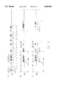
- FIG. 1 is a block diagram illustrating a transmitter and receiver of the device of the present invention.
- FIG. 2 is a schematic diagram showing the structure of a data generator of the transmitter of the present invention.
- FIG. 3(a through c) are impulse diagrams illustrating the method of the present invention.
- FIG. 4 is a block diagram illustrating a decoder 16 for decoding the biphase/Manchester code.
- FIG. 1 is a schematic diagram which shows a transmitter and receiver of a device for implementing the method of the present invention.
- the transmitter 30 (and receiver 20) may include a known device 10 for transmitting binary coded data signals such as, for example, from European Patent Application No. EP 0 191 019 B1.
- the transmitting side of such a known device 10 is coupled with one or more data generators 1, 2, each data generator having an assigned data channel.
- the outputs of the data generators 1, 2 are coupled, via data lines 4, 5, with the inputs of a linking stage 3.
- the linking stage 3 links (i.e., combines) the data signals of the data generators 1, 2 into a single output signal DL3, and may comprise commercially available gate circuits 6 (e.g. AND elements) which join inputted signals together into a new signal.
- gate circuits 6 e.g. AND elements
- the output signal DL3 is modulated in a modulator 8 and broadcast via an antenna 7, together with the carrier frequency of the transmitter.
- the data signals may be transmitted pursuant to the semipassive transponder method.
- a cycle signal T is provided to synchronize the data generators 1, 2.
- the cycle signal T may be formed by the data generator 2, for example, and applied to a control input of the data generator 1.
- FIG. 2 is a schematic which shows the basic structure of the data generators 1, 2.
- the cycle generator 31 is coupled with an input of a logic circuit 32 (exclusive OR).
- the data signal to be transmitted is applied to a second input of the logic circuit 32.
- the logic circuit 32 includes an output which provides the data signal DL1 or DL2, respectively. This signal is provided to an input of the linking stage 3.
- the linked signal DL3 is provided to the antenna 7 via the modulator 8.
- the receiver 20 is provided with a reception antenna 15 coupled with a demodulator 17.
- One or more filters 11, 12 are provided between a decoder 16 and the demodulator 17. These filters 11, 12 separate the incoming data signal DL3 in accordance with the transmitted data signals.
- the filters 11, 12 are structured as a known band pass filter or frequency diplexer.
- the demodulator 17 is also commercially available.
- the separated data signals are passed to inputs of a commercially available decoder 16 on separate lines 13, 14. Depending on which transmission channel the receiver 20 is set, decoding takes place only for the data signal which was intended for this receiver.
- FIG. 4 is a block diagram showing the decoder 16 for decoding the biphase/Manchester code.
- the incoming data signal DL1 or DL2 on the line 13 or 14, respectively, is passed via a comparator 41 for signal formation reasons.
- the cycle frequency for the BIT period depicted in FIG. 3 is derived from the data signal DL1 or DL2 by element 42. Actual decoding takes place by means of two subsequent D flip-flops 43 and 44.
- the output signals of the D flip-flops 43 and 44 are provided to inputs of a linking circuit 45.
- the output signals of the D flip-flops 43 and 44 are combined as a function of the related cycle signal.
- the decoded data signal DL1 or DL2 is provided at an output of the linking circuit 45.
- the receiver 20 may be structured to receive and evaluate only traffic guidance data. In such a case, the receiver 20 decodes only the signals of the data signal DL1 with its decoder 16. Another receiver, on the other hand, can also decode the data signal DL2, or decode only a signal used for billing road use fees, for example.
- a typical application of data signal transmission is bi-directional data transmission between a motor vehicle and a fixed beacon at the side of the road.
- road traffic data, road maps or recommended driving directions can be transmitted from the beacon to the motor vehicle.
- transmitting navigation data for example concerning the location of the vehicle within the scope of fleet management, is also possible.
- the device for implementing the method of the present invention only one transmission channel is used to transmit the transmission signal DL3.
- this channel is modulated with the two data signals of the data generators 1, 2. It is practical to modulate the channel according to the amplitude modulation method (amplitude shift keying, ASK) and/or the frequency modulation method (frequency shift keying, FSK).
- ASK amplitude shift keying
- FSK frequency shift keying
- the biphase/Manchester method is preferably provided.
- the signals from two signal elements are brought together, phase-shifted by 180° (See, e.g., Conrads, Moderne Ltdunikationstechnik, pages 36-37; or W. Lee, Mobile Communications Engineering, pages 342-343).
- FIGS. 3a-3c are timing diagrams which illustrate the method of the present invention as effected by the circuit arrangement.
- FIG. 3a illustrates the data signal DL1 of the data line 4.
- the data signal DL1 for example, operates at a carrier frequency RF of 5.8 GHz.
- the time axis is divided into 18 BIT periods 1 . . . 18, where the duration of one bit period is 2 ⁇ T1.
- the carrier signal RF appears in the second half period, while no signal appears in the first half period.
- This first bit period corresponds to logic ⁇ 0 ⁇ .
- the carrier signal RF appears in the first half period but does not appear in the second half period. This represents the value logic ⁇ 1 ⁇ .
- the logic signals ⁇ 0 ⁇ and ⁇ 1 ⁇ are coded in accordance with the desired data by the data generator 1.
- FIG. 3b illustrates the data signal DL2.
- the period duration T2 of the data signal DL2 is 8 times as long as the present duration T1 of the data signal DL1. Coding with logic ⁇ 0 ⁇ and ⁇ 1 ⁇ values takes place in the same manner as for data signal DL1.
- FIG. 3c illustrates the signal DL3.
- the signal DL3 is transmitted after modulation with a commercially available modulator 8, via the antenna 7, and received by the antenna 15.
- the data signal DL1 and the data signal DL2 are decoded from this signal.
- the data signal DL1 contains traffic guidance data
- the low-frequency data signal DL2 can be used for billing road use fees, parking lot fees, etc.
- corresponding reception devices can then be used, which process both signals jointly or can evaluate them individually.
- a simple device for billing the road use fee to the receiver is possible without changing the transmission side.
- This device then evaluates only the data signal DL2.
- the data signal DL1 can be evaluated with a different device, for example with a location and navigation device.
- This device can also be coupled with the receiver 20.
Priority Applications (1)
| Application Number | Priority Date | Filing Date | Title |
|---|---|---|---|
| US08/456,410 US5650996A (en) | 1992-10-24 | 1995-06-01 | Method and circuit arrangement for combining several digital data channels on a transmission channel |
Applications Claiming Priority (4)
| Application Number | Priority Date | Filing Date | Title |
|---|---|---|---|
| DE4236002A DE4236002A1 (de) | 1992-10-24 | 1992-10-24 | Verfahren und Schaltungsanordnung zur Verbindung mehrerer digitaler Datenkanäle zu einem Übertragungskanal |
| DE4236002.1 | 1992-10-24 | ||
| US14273293A | 1993-10-25 | 1993-10-25 | |
| US08/456,410 US5650996A (en) | 1992-10-24 | 1995-06-01 | Method and circuit arrangement for combining several digital data channels on a transmission channel |
Related Parent Applications (1)
| Application Number | Title | Priority Date | Filing Date |
|---|---|---|---|
| US14273293A Continuation | 1992-10-24 | 1993-10-25 |
Publications (1)
| Publication Number | Publication Date |
|---|---|
| US5650996A true US5650996A (en) | 1997-07-22 |
Family
ID=6471302
Family Applications (1)
| Application Number | Title | Priority Date | Filing Date |
|---|---|---|---|
| US08/456,410 Expired - Lifetime US5650996A (en) | 1992-10-24 | 1995-06-01 | Method and circuit arrangement for combining several digital data channels on a transmission channel |
Country Status (3)
| Country | Link |
|---|---|
| US (1) | US5650996A (de) |
| EP (1) | EP0595019A3 (de) |
| DE (1) | DE4236002A1 (de) |
Cited By (4)
| Publication number | Priority date | Publication date | Assignee | Title |
|---|---|---|---|---|
| US6246664B1 (en) * | 1997-04-18 | 2001-06-12 | Alcatel | Modulator for modulating digital signals |
| US20020042878A1 (en) * | 2000-09-01 | 2002-04-11 | Andreas Westendorf | Data transmission method |
| US20070042759A1 (en) * | 2004-04-28 | 2007-02-22 | Woong Kim | System and method for providing mileage on wireless network |
| WO2011149425A1 (en) * | 2010-05-26 | 2011-12-01 | Agency For Science, Technology And Research (A*Star) | Phase shift keying transmitter circuit |
Families Citing this family (1)
| Publication number | Priority date | Publication date | Assignee | Title |
|---|---|---|---|---|
| DE4344578A1 (de) * | 1993-12-24 | 1995-06-29 | Zimmer Hans J | Zentralverriegelung |
Citations (8)
| Publication number | Priority date | Publication date | Assignee | Title |
|---|---|---|---|---|
| GB2146875A (en) * | 1983-09-09 | 1985-04-24 | Racal Res Ltd | Communications systems |
| EP0191019A1 (de) * | 1984-07-26 | 1986-08-20 | Bosch Gmbh Robert | Einrichtung zum übertragen von binären daten zwischen einem mobilen datenträger und einer feststation. |
| GB2220824A (en) * | 1988-07-13 | 1990-01-17 | Philips Electronic Associated | Transmission system for sending two signals simultaneously on the same communications channel |
| US4899350A (en) * | 1986-05-16 | 1990-02-06 | Nec Corporation | Signal communication capable of avoiding an audible reproduction of a sequence of information signals |
| US4903125A (en) * | 1986-04-17 | 1990-02-20 | British Broadcasting Corporation | Method and apparatus for conveying information signals |
| DE3839421A1 (de) * | 1988-11-18 | 1990-05-23 | Licentia Gmbh | Einrichtung zur pegeleinbruchfreien drahtlosen uebertragung von modulierten hf-signalen |
| US4972408A (en) * | 1988-04-29 | 1990-11-20 | Alcatel Cit | Method and apparatus for combining and for separating a low data rate digital channel with or from the high data rate digital channel of a transmission link |
| US5012489A (en) * | 1988-11-07 | 1991-04-30 | Hayes Microcomputer Products, Inc. | Method for sending a plurality of data channels over a single communications line |
-
1992
- 1992-10-24 DE DE4236002A patent/DE4236002A1/de not_active Withdrawn
-
1993
- 1993-09-21 EP EP93115146A patent/EP0595019A3/de not_active Withdrawn
-
1995
- 1995-06-01 US US08/456,410 patent/US5650996A/en not_active Expired - Lifetime
Patent Citations (9)
| Publication number | Priority date | Publication date | Assignee | Title |
|---|---|---|---|---|
| GB2146875A (en) * | 1983-09-09 | 1985-04-24 | Racal Res Ltd | Communications systems |
| EP0191019A1 (de) * | 1984-07-26 | 1986-08-20 | Bosch Gmbh Robert | Einrichtung zum übertragen von binären daten zwischen einem mobilen datenträger und einer feststation. |
| US4665399A (en) * | 1984-07-26 | 1987-05-12 | Robert Bosch Gmbh | Device for transmitting of binary data between a mobile data carrier and a stationary station |
| US4903125A (en) * | 1986-04-17 | 1990-02-20 | British Broadcasting Corporation | Method and apparatus for conveying information signals |
| US4899350A (en) * | 1986-05-16 | 1990-02-06 | Nec Corporation | Signal communication capable of avoiding an audible reproduction of a sequence of information signals |
| US4972408A (en) * | 1988-04-29 | 1990-11-20 | Alcatel Cit | Method and apparatus for combining and for separating a low data rate digital channel with or from the high data rate digital channel of a transmission link |
| GB2220824A (en) * | 1988-07-13 | 1990-01-17 | Philips Electronic Associated | Transmission system for sending two signals simultaneously on the same communications channel |
| US5012489A (en) * | 1988-11-07 | 1991-04-30 | Hayes Microcomputer Products, Inc. | Method for sending a plurality of data channels over a single communications line |
| DE3839421A1 (de) * | 1988-11-18 | 1990-05-23 | Licentia Gmbh | Einrichtung zur pegeleinbruchfreien drahtlosen uebertragung von modulierten hf-signalen |
Non-Patent Citations (8)
| Title |
|---|
| Bode et al., Bit Error Measurements on a 5.8 GHz Mobile Radio Channel for Short Range Traffic Management Systems . * |
| Bode et al., Bit Error Measurements on a 5.8 GHz Mobile Radio Channel for Short Range Traffic Management Systems. |
| Dieter Conrads, Moderne Kommunikationstechnik Dataenkommunikation, Mit 116 Abbildungen und 9 Tabellen, 1989, pp. 34 37. * |
| Dieter Conrads, Moderne Kommunikationstechnik-Dataenkommunikation, Mit 116 Abbildungen und 9 Tabellen, 1989, pp. 34-37. |
| European Radiocommunications Committee ( ERC ), Report from the European Radiocommunications Committee within CEPT on the harmonization of frequency bands to be designated for Road transport Information Systems, ERC Report 3, Lisbon, Feb. 1991. * |
| European Radiocommunications Committee ( ERC), Report from the European Radiocommunications Committee within CEPT on the harmonization of frequency bands to be designated for Road transport Information Systems, ERC Report 3, Lisbon, Feb. 1991. |
| William C.Y. Lee, Mobile Communications Engineering, McGraw Hill Book Company, 1982, pp. 342 343. * |
| William C.Y. Lee, Mobile Communications Engineering, McGraw-Hill Book Company, 1982, pp. 342-343. |
Cited By (6)
| Publication number | Priority date | Publication date | Assignee | Title |
|---|---|---|---|---|
| US6246664B1 (en) * | 1997-04-18 | 2001-06-12 | Alcatel | Modulator for modulating digital signals |
| US20020042878A1 (en) * | 2000-09-01 | 2002-04-11 | Andreas Westendorf | Data transmission method |
| US7712139B2 (en) * | 2000-09-01 | 2010-05-04 | Robert Bosch Gmbh | Data transmission method |
| US20070042759A1 (en) * | 2004-04-28 | 2007-02-22 | Woong Kim | System and method for providing mileage on wireless network |
| WO2011149425A1 (en) * | 2010-05-26 | 2011-12-01 | Agency For Science, Technology And Research (A*Star) | Phase shift keying transmitter circuit |
| US8976901B2 (en) | 2010-05-26 | 2015-03-10 | Agency For Science, Technology And Research | Phase shift keying transmitter circuit |
Also Published As
| Publication number | Publication date |
|---|---|
| DE4236002A1 (de) | 1994-04-28 |
| EP0595019A3 (de) | 1995-03-01 |
| EP0595019A2 (de) | 1994-05-04 |
Similar Documents
| Publication | Publication Date | Title |
|---|---|---|
| US4425666A (en) | Data encoding and decoding communication system for three frequency FSK modulation and method therefor | |
| CA1241378A (en) | Multi-speed, full duplex modem | |
| US5650996A (en) | Method and circuit arrangement for combining several digital data channels on a transmission channel | |
| US4613973A (en) | Digital data decoder and method | |
| JPS6214535A (ja) | 無線送信システム | |
| US4333078A (en) | Apparatus for synchronized reception in connection with system for recording objects | |
| CN86105925A (zh) | 大容量信道尤其是卫星传输信道上数字信号群的传输方法和接收装置 | |
| US4388726A (en) | System for the ultra-high frequency transmission of numerical data | |
| US20030076897A1 (en) | Digital transmission method for bandwidth and bit rate flexibility | |
| US6463104B1 (en) | Method of increasing coding levels | |
| KR100254127B1 (ko) | 디지탈 발진기 | |
| US5295160A (en) | Apparatus for FM-modulation of digital signals | |
| US4464766A (en) | Radio transmission system for binary coded signals | |
| KR970704274A (ko) | 통신 시스템 및 그것을 위한 전송수단 | |
| US5450454A (en) | Coding and decoding a modulated radio frequency signal | |
| US5073903A (en) | Information transmission arrangement using frequency modulation | |
| JP2000134269A5 (de) | ||
| WO1992014307A1 (en) | Method of achieving a closed synchronization loop for two-way communication between a transponder and an interrogator, where different frequencies can be used for the communication between the interrogator and the transponder | |
| SU1083383A1 (ru) | Многоканальна система св зи | |
| US3913019A (en) | Double quadrature fm receiver | |
| SU1290557A1 (ru) | Система дл передачи и приема дискретной информации | |
| RU1800631C (ru) | Многоканальна цифрова система св зи | |
| RU2316114C2 (ru) | Линия радиосвязи с многопараметрической модуляцией | |
| JPH04150498A (ja) | 通信システム | |
| SU801280A1 (ru) | Многолучева система радиосв зи |
Legal Events
| Date | Code | Title | Description |
|---|---|---|---|
| STCF | Information on status: patent grant |
Free format text: PATENTED CASE |
|
| FEPP | Fee payment procedure |
Free format text: PAYOR NUMBER ASSIGNED (ORIGINAL EVENT CODE: ASPN); ENTITY STATUS OF PATENT OWNER: LARGE ENTITY |
|
| FPAY | Fee payment |
Year of fee payment: 4 |
|
| FPAY | Fee payment |
Year of fee payment: 8 |
|
| FPAY | Fee payment |
Year of fee payment: 12 |