US5552331A - Process for self-aligned source for high density memory - Google Patents
Process for self-aligned source for high density memory Download PDFInfo
- Publication number
- US5552331A US5552331A US08/500,648 US50064895A US5552331A US 5552331 A US5552331 A US 5552331A US 50064895 A US50064895 A US 50064895A US 5552331 A US5552331 A US 5552331A
- Authority
- US
- United States
- Prior art keywords
- gate
- providing
- spacers
- semiconductor body
- transistor
- Prior art date
- Legal status (The legal status is an assumption and is not a legal conclusion. Google has not performed a legal analysis and makes no representation as to the accuracy of the status listed.)
- Expired - Lifetime
Links
- 238000000034 method Methods 0.000 title claims abstract description 34
- 125000006850 spacer group Chemical group 0.000 claims abstract description 51
- 239000004065 semiconductor Substances 0.000 claims abstract description 27
- XUIMIQQOPSSXEZ-UHFFFAOYSA-N Silicon Chemical compound [Si] XUIMIQQOPSSXEZ-UHFFFAOYSA-N 0.000 claims description 17
- 238000005530 etching Methods 0.000 claims description 17
- 229910052710 silicon Inorganic materials 0.000 claims description 17
- 239000010703 silicon Substances 0.000 claims description 17
- 239000007943 implant Substances 0.000 claims description 8
- 238000002513 implantation Methods 0.000 claims description 4
- 238000004519 manufacturing process Methods 0.000 claims description 3
- 230000000903 blocking effect Effects 0.000 claims description 2
- 150000002500 ions Chemical class 0.000 claims 6
- 230000015572 biosynthetic process Effects 0.000 abstract description 3
- 239000000758 substrate Substances 0.000 description 15
- 230000000873 masking effect Effects 0.000 description 14
- 229910021420 polycrystalline silicon Inorganic materials 0.000 description 5
- 229920005591 polysilicon Polymers 0.000 description 5
- 239000010409 thin film Substances 0.000 description 5
- 238000009792 diffusion process Methods 0.000 description 3
- 229920002120 photoresistant polymer Polymers 0.000 description 3
- 230000015556 catabolic process Effects 0.000 description 2
- 238000005468 ion implantation Methods 0.000 description 2
- 239000000463 material Substances 0.000 description 2
- 238000007796 conventional method Methods 0.000 description 1
- 230000008021 deposition Effects 0.000 description 1
- 239000003989 dielectric material Substances 0.000 description 1
- 238000009826 distribution Methods 0.000 description 1
- -1 etches Substances 0.000 description 1
- 239000010408 film Substances 0.000 description 1
- 230000006870 function Effects 0.000 description 1
- 238000012986 modification Methods 0.000 description 1
- 230000004048 modification Effects 0.000 description 1
- 150000004767 nitrides Chemical class 0.000 description 1
- 238000000059 patterning Methods 0.000 description 1
Images


Classifications
-
- H—ELECTRICITY
- H10—SEMICONDUCTOR DEVICES; ELECTRIC SOLID-STATE DEVICES NOT OTHERWISE PROVIDED FOR
- H10B—ELECTRONIC MEMORY DEVICES
- H10B41/00—Electrically erasable-and-programmable ROM [EEPROM] devices comprising floating gates
- H10B41/40—Electrically erasable-and-programmable ROM [EEPROM] devices comprising floating gates characterised by the peripheral circuit region
-
- H—ELECTRICITY
- H10—SEMICONDUCTOR DEVICES; ELECTRIC SOLID-STATE DEVICES NOT OTHERWISE PROVIDED FOR
- H10B—ELECTRONIC MEMORY DEVICES
- H10B69/00—Erasable-and-programmable ROM [EPROM] devices not provided for in groups H10B41/00 - H10B63/00, e.g. ultraviolet erasable-and-programmable ROM [UVEPROM] devices
-
- H—ELECTRICITY
- H01—ELECTRIC ELEMENTS
- H01L—SEMICONDUCTOR DEVICES NOT COVERED BY CLASS H10
- H01L27/00—Devices consisting of a plurality of semiconductor or other solid-state components formed in or on a common substrate
- H01L27/02—Devices consisting of a plurality of semiconductor or other solid-state components formed in or on a common substrate including semiconductor components specially adapted for rectifying, oscillating, amplifying or switching and having potential barriers; including integrated passive circuit elements having potential barriers
- H01L27/04—Devices consisting of a plurality of semiconductor or other solid-state components formed in or on a common substrate including semiconductor components specially adapted for rectifying, oscillating, amplifying or switching and having potential barriers; including integrated passive circuit elements having potential barriers the substrate being a semiconductor body
- H01L27/10—Devices consisting of a plurality of semiconductor or other solid-state components formed in or on a common substrate including semiconductor components specially adapted for rectifying, oscillating, amplifying or switching and having potential barriers; including integrated passive circuit elements having potential barriers the substrate being a semiconductor body including a plurality of individual components in a repetitive configuration
- H01L27/105—Devices consisting of a plurality of semiconductor or other solid-state components formed in or on a common substrate including semiconductor components specially adapted for rectifying, oscillating, amplifying or switching and having potential barriers; including integrated passive circuit elements having potential barriers the substrate being a semiconductor body including a plurality of individual components in a repetitive configuration including field-effect components
-
- H—ELECTRICITY
- H10—SEMICONDUCTOR DEVICES; ELECTRIC SOLID-STATE DEVICES NOT OTHERWISE PROVIDED FOR
- H10B—ELECTRONIC MEMORY DEVICES
- H10B41/00—Electrically erasable-and-programmable ROM [EEPROM] devices comprising floating gates
- H10B41/40—Electrically erasable-and-programmable ROM [EEPROM] devices comprising floating gates characterised by the peripheral circuit region
- H10B41/42—Simultaneous manufacture of periphery and memory cells
- H10B41/43—Simultaneous manufacture of periphery and memory cells comprising only one type of peripheral transistor
-
- H—ELECTRICITY
- H10—SEMICONDUCTOR DEVICES; ELECTRIC SOLID-STATE DEVICES NOT OTHERWISE PROVIDED FOR
- H10B—ELECTRONIC MEMORY DEVICES
- H10B99/00—Subject matter not provided for in other groups of this subclass
Definitions
- This invention relates to semiconductor devices, and more particularly, to a semiconductor structure which combines memory cells with remote periphery transistors.
- FIGS. 1-3 related to U.S. Pat. No. 5,120,671 to Tang et al., issued Jun. 9, 1992, show high density self-aligned-source flash memory cells fabricated by using a conventional process.
- FIG. 1 is a plan view of a portion of a memory device formed in that manner.
- Field oxide regions 10, 12 are formed as continuous lines across the source line 14 in the substrate 15.
- a gate oxide layer is formed on the substrate areas between field oxide lines, followed by deposition and patterning of a first polysilicon layer, and formation of an intergate dielectric layer.
- a second layer of polysilicon 16 is deposited and, after appropriate masking, exposed portions of the polysilicon are etched away forming control gate regions 18, 20 (word lines).
- etching steps are used to remove intergate dielectric and first polysilicon exposed between word lines.
- a photoresist mask exposing the source regions is then applied over the device.
- Exposed field oxide regions 10, 12 are etched away using an oxide etch process selective to silicon, forming a source line connecting source regions 14. This continuous source line is parallel to and self-aligned to the edges of the previously defined word lines.
- FIGS. 2 and 3 are sectional views taken along the lines 2--2 and 3--3 of FIG. 1 respectively, prior to the etching of the field oxide regions 10, 12.
- FIG. 2 shows a first stack 22 made up of gate oxide 24-floating gate 26-intergate dielectric 28-control gate 30, and a second stack 32 made up of gate oxide 34-floating gate 36-intergate dielectric 38-control gate 40 with source 42 and drains 44, 46 in the substrate 48 self-aligned to the edges of the control gates 30, 40.
- the word lines 18, 20 define the control gates 30, 40 respectively and extend over the field oxide regions such as regions 10, 12 (FIG. 3).
- FIGS. 4 through 9 the process as shown in FIGS. 4 through 9 has been used.
- FIGS. 4 through 9 includes sectional views 4a, 4b, and 4c, FIGS. 4a and 4b corresponding to the sectional views of FIGS. 2 and 3, while FIG. 4c is a sectional view of a periphery transistor in the same intergated circuit.
- FIGS. 5-9 follow the same convention, as do FIGS. 10-14).
- a silicon substrate 130 is provided with a gate oxide 132 formed thereover.
- a first floating gate 134-intergate dielectric 136-control gate 138 stack 140 is provided on the oxide layer 132, and a second floating gate 142-intergate dielectric 144-control gate 146 stack 148 is also provided on the oxide layer 132, spaced from the stack 140.
- a source region 150 is provided in the substrate 130, self-aligned to the adjacent edges of the stacks 140, 148. Drain regions 152, 154 are also included in the substrate 130, self-aligned to the respective opposite edges of the stacks 140, 148.
- the control gates 138, 146 extend over field oxide 156 (FIG. 4b), which in turn lies over substrate 130.
- a high voltage periphery transistor 158 Remote from the structure of FIGS. 4a and 4b is a high voltage periphery transistor 158 (FIG. 4c) including a gate oxide 160 on the substrate 130, and a gate 162, with lightly-doped source and drain regions 164, 166 being self-aligned to the edges of the gate 162.
- oxide 168 Over this structure is deposited a thick (for example 3000 ⁇ ) layer of oxide 168. This deposited oxide 168 is then anisotropically etched to form relatively wide spacers 170, 172, 174, 176 on the sides of each stack 140, 148, relatively wide spacers 178, 180 on the adjacent sides of the control gates 138, 146 over the field oxide 156, and relatively wide spacers 182, 184 on the sides of the gate 162 of the high voltage periphery transistor 158.
- This deposited oxide 168 is then anisotropically etched to form relatively wide spacers 170, 172, 174, 176 on the sides of each stack 140, 148, relatively wide spacers 178, 180 on the adjacent sides of the control gates 138, 146 over the field oxide 156, and relatively wide spacers 182, 184 on the sides of the gate 162 of the high voltage periphery transistor 158.
- the relatively wide spacers 182, 184 on the sides of the gate 162 of the high voltage periphery transistor 158 are properly configured so that subsequently-formed heavily doped source and drain regions will be self-aligned to the spacers 182, 184 and properly positioned in relation to the lightly doped source and drain regions 164, 166.
- Such wide spacers 182, 184 are necessary to meet high transistor junction breakdown requirements.
- provision of such relatively wide spacers 178, 180 on the inner sides of the control gates 138, 140 over the field oxide 156 causes certain problems, as will now be described.
- masking 186 is provided over appropriate areas of the structure, and further anisotropic etching is undertaken. Such etching is undertaken through the thin oxide layer 132 (FIG. 6a), and also through the field oxide 156 (FIG. 6b), it being noted that the exposed width (dimension X) of the silicon 130 due to etching through of the field oxide 156 is relatively small, because of the initial large width of the spacers 178, 180. In the meantime, etchant cannot reach the high-voltage periphery transistor 158 due to masking 186 thereover.
- a thin layer of oxide 188 is grown over the exposed portion of the silicon 130 between the stacks 140, 148, and a thin layer of oxide 190 is grown over the exposed portion of the silicon 130 provided by the opening in the field oxide 156 (FIG. 7b) simultaneously forming thin oxide layers 188, 190 and 191.
- ion implantation 194 is undertaken through the grown thin layers of oxide 188, 190, and a diffusion step is undertaken so that the source region 150 takes the shape shown in FIG. 9a, and the diffused area 196 adjacent the field oxide (FIG. 9b) provides connection between the source region 150 and other source regions. Further processing steps are then provided to form heavily doped source and drain regions 198, 200 of the periphery transistor 158, self aligned to the spacers 182, 184.
- the present invention overcomes the above-cited problems by initially forming flash memory transistor source and drain junctions and then providing a relatively thin layer of deposited oxide over floating gate-intergate dielectric-control gate stacks of flash memory transistors, over the control gate extensions on field oxide, and over the gate oxide and gate of a high voltage periphery transistor. After appropriate masking, this deposited thin oxide is etched to provide relatively narrow spacers on the adjacent sides of the stack, and on the adjacent sides of the control gate over the field oxide. The field oxide is subsequently etched through while source junctions are protected by the spacers on adjacent sides of the stacks. The deposited thin oxide over the periphery transistor is blocked by masking at this point.
- the deposited thin oxide is used as an implant blocking mask, thus saving one photoresist masking step in the process. Because the spacers are relatively narrow, the portion of silicon exposed by etching through the field oxide is relatively wide so that a relatively large width of silicon is exposed to implant, so that low series resistance between the sources of devices is provided.
- the preferred relatively wide spacers are provided on the opposite sides of the gate of the periphery transistor, so that the heavily doped source and drain regions of the periphery transistor are self-aligned to the edges of those wide spacers to render high junction breakdown for the periphery transistor.
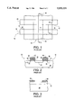
- FIG. 1 is a plan view of a typical flash memory structure of the prior art
- FIG. 2 is a sectional view taken along the line 2--2 of FIG. 1;
- FIG. 3 is a sectional view taken along the line 3--3 of FIG. 1;
- FIGS. 4a-4c, 5a-5c, 6a-6c, 7a-7c, 8a-8c, 9a-9c are a series of cross sectional views showing the process flow of another flash memory system.
- FIGS. 10a-10c, 11a-11c, 12a-12c, 13a-13c, 14a-14c are cross sectional views showing the process flow of the present invention.
- FIG. 10 illustrates sectional views of several areas of a partially processed flash EPROM memory device.
- FIG. 10a shows a pair of transistors as thus far formed, including a semiconductor substrate 220 of for example p-type silicon on which is provided a gate oxide 222, a first stack 224 (including a floating gate 226 on the gate oxide 222, an intergate dielectric layer 228, and a control gate 230), and a second stack 232 (including a floating gate 234 on the gate oxide 222, an intergate dielectric layer 236 and a control gate 238).
- An n-type source region 239 is provided in the substrate 220, self-aligned to the adjacent edges of the respective stacks 224, 232.
- FIG. 10b shows the structure adjacent to the structure of FIG. 10a, with extensions of the control gates 230, 238 over the field oxide 240, which in turn lies over the substrate 220
- FIG. 10c shows a high voltage remote periphery transistor 242 in an area removed from the structures of FIG. 10a and 10b, and which includes a gate oxide 244 over the substrate 220, a gate 246, and lightly doped source and drain regions 248, 250 aligned to the edges of the gate 246.
- a thin film layer 252 is deposited over the structure as shown in FIG. 10a, 10b and 10c.
- This thin film layer 252 may take the form of an oxide, nitride, polysilicon or a combination thereof, or any dielectric.
- the resulting structure is appropriately masked (254) as shown in FIG. 11, and is anisotropically etched to provide relatively narrow spacers 256, 258 on the adjacent sides of the respect stacks 224, 232, and relatively narrow spacers 260, 262 on the adjacent sides of the control gates 230, 238 over the field oxide 240.
- the etching is continued through the layer of oxide 222 and into the substrate 220, and also through the field oxide 240 down to the substrate 220. Meanwhile, the periphery transistor 242 remains covered by a photoresist mask.
- the width Y (FIG. 11b) of exposed silicon caused by etching through the field oxide 240 is relatively large.
- a thin layer of oxide is grown over the exposed silicon areas, at 264 and 266.
- Ion implantation 268 is then undertaken, self aligned to the spacers 256, 258 and spacers 260, 262, it being noted that because of the relatively thin spacers 256, 258, 260, 262, the implant covers a substantially wider area between the stacks 224, 232 and between the portions of field oxide 240 than in the prior art. It will then be seen that after diffusion of this implant (FIG. 13), the connection 269 between memory transistor sources is much wider than in the prior art, resulting in a much lower series resistance from source to source in the ultimately formed structure.
- thin film layer 252 blocks implant 268 from reaching the source and drain regions of periphery transistor 242 (FIG. 12c). Note that a resist masking step is not required to protect periphery transistors during this implant.
- Another anisotropic etch is undertaken, resulting in relatively wide spacers 280, 282 on the opposite sides of the gate 246 of the transistor 242 so that the heavily doped regions 284, 286 subsequently formed can be properly self-aligned to the sides of those spacers 280, 282 and provide proper dimensioning in regard to the lightly doped regions 248, 250.
- Flash EPROM memory Flash EPROM memory
Landscapes
- Engineering & Computer Science (AREA)
- Power Engineering (AREA)
- Manufacturing & Machinery (AREA)
- Physics & Mathematics (AREA)
- Condensed Matter Physics & Semiconductors (AREA)
- General Physics & Mathematics (AREA)
- Computer Hardware Design (AREA)
- Microelectronics & Electronic Packaging (AREA)
- Semiconductor Memories (AREA)
- Non-Volatile Memory (AREA)
Abstract
Description
Claims (20)
Priority Applications (6)
| Application Number | Priority Date | Filing Date | Title |
|---|---|---|---|
| US08/500,648 US5552331A (en) | 1995-07-11 | 1995-07-11 | Process for self-aligned source for high density memory |
| KR1019970701600A KR100418430B1 (en) | 1995-07-11 | 1996-06-21 | Process for self-aligned source for high density memory |
| PCT/US1996/010698 WO1997003470A1 (en) | 1995-07-11 | 1996-06-21 | Process for self-aligned source for high density memory |
| EP96922531A EP0780023B1 (en) | 1995-07-11 | 1996-06-21 | Process for self-aligned source for high density memory |
| JP50582297A JP3941882B2 (en) | 1995-07-11 | 1996-06-21 | Process for self-aligned source for high density memory |
| DE69620559T DE69620559T2 (en) | 1995-07-11 | 1996-06-21 | METHOD FOR SELF-ALIGNED SOURCE IN A HIGH DENSITY STORAGE |
Applications Claiming Priority (1)
| Application Number | Priority Date | Filing Date | Title |
|---|---|---|---|
| US08/500,648 US5552331A (en) | 1995-07-11 | 1995-07-11 | Process for self-aligned source for high density memory |
Publications (1)
| Publication Number | Publication Date |
|---|---|
| US5552331A true US5552331A (en) | 1996-09-03 |
Family
ID=23990342
Family Applications (1)
| Application Number | Title | Priority Date | Filing Date |
|---|---|---|---|
| US08/500,648 Expired - Lifetime US5552331A (en) | 1995-07-11 | 1995-07-11 | Process for self-aligned source for high density memory |
Country Status (6)
| Country | Link |
|---|---|
| US (1) | US5552331A (en) |
| EP (1) | EP0780023B1 (en) |
| JP (1) | JP3941882B2 (en) |
| KR (1) | KR100418430B1 (en) |
| DE (1) | DE69620559T2 (en) |
| WO (1) | WO1997003470A1 (en) |
Cited By (24)
| Publication number | Priority date | Publication date | Assignee | Title |
|---|---|---|---|---|
| US5736442A (en) * | 1995-09-14 | 1998-04-07 | Kabushiki Kaisha Toshiba | Method of manufacturing a semiconductor memory device |
| US5792695A (en) * | 1996-05-31 | 1998-08-11 | Sanyo Electric Co., Ltd. | Manufacturing method of a semiconductor eprom device |
| US5854108A (en) * | 1996-06-04 | 1998-12-29 | Advanced Micro Devices, Inc. | Method and system for providing a double diffuse implant junction in a flash device |
| US5933730A (en) * | 1997-03-07 | 1999-08-03 | Advanced Micro Devices, Inc. | Method of spacer formation and source protection after self-aligned source is formed and a device provided by such a method |
| US5989986A (en) * | 1997-03-13 | 1999-11-23 | United Microelectronics Corp. | Method to inhibit the formation of ion implantation induced edge defects |
| US6001687A (en) * | 1999-04-01 | 1999-12-14 | Taiwan Semiconductor Manufacturing Company, Ltd. | Process for forming self-aligned source in flash cell using SiN spacer as hard mask |
| US6017796A (en) * | 1998-06-18 | 2000-01-25 | United Semiconductor Corp. | Method of fabricating flash electrically-erasable and programmable read-only memory (EEPROM) device |
| US6025240A (en) * | 1997-12-18 | 2000-02-15 | Advanced Micro Devices, Inc. | Method and system for using a spacer to offset implant damage and reduce lateral diffusion in flash memory devices |
| US6027971A (en) * | 1996-07-16 | 2000-02-22 | Samsung Electronics Co., Ltd. | Methods of forming memory devices having protected gate electrodes |
| US6069383A (en) * | 1997-12-31 | 2000-05-30 | Lg Semicon Co., Ltd. | Flash memory and method for fabricating the same |
| US6140191A (en) * | 1998-09-21 | 2000-10-31 | Advanced Micro Devices, Inc. | Method of making high performance MOSFET with integrated simultaneous formation of source/drain and gate regions |
| WO2001071803A1 (en) * | 2000-03-17 | 2001-09-27 | Advanced Micro Devices, Inc. | A dual spacer process for non-volatile memory devices |
| US6344398B1 (en) * | 2000-10-17 | 2002-02-05 | United Microelectronics Corp. | Method for forming transistor devices with different spacer width |
| US6392267B1 (en) | 1997-04-25 | 2002-05-21 | Alliance Semiconductor Corporation | Flash EPROM array with self-aligned source contacts and programmable sector erase architecture |
| US6624022B1 (en) | 2000-08-29 | 2003-09-23 | Micron Technology, Inc. | Method of forming FLASH memory |
| US6649968B2 (en) | 1999-03-01 | 2003-11-18 | Micron Technology, Inc. | Flash memory cells |
| US6706601B1 (en) * | 2003-03-19 | 2004-03-16 | Taiwan Semiconductor Manufacturing Company | Method of forming tiny silicon nitride spacer for flash EPROM by using dry+wet etching technology |
| US20050070067A1 (en) * | 2003-09-25 | 2005-03-31 | Kim In Su | Methods of fabricating semiconductor devices |
| US20060086985A1 (en) * | 2004-10-18 | 2006-04-27 | Motoya Kishida | Semiconductor device |
| US20060263969A1 (en) * | 2005-05-19 | 2006-11-23 | Hwang David K | Method of manufacturing sidewall spacers on a memory device, and device comprising same |
| DE19708031B4 (en) * | 1996-09-04 | 2008-04-30 | Oki Electric Industry Co., Ltd. | Non-volatile semiconductor memory and method for its production |
| US20080286922A1 (en) * | 2007-05-18 | 2008-11-20 | Dongbu Hitek Co., Ltd. | Method of fabricating semiconductor device |
| US7888198B1 (en) * | 1998-05-20 | 2011-02-15 | Samsung Electronics Co., Ltd. | Method of fabricating a MOS transistor with double sidewall spacers in a peripheral region and single sidewall spacers in a cell region |
| US10216523B2 (en) | 2015-07-17 | 2019-02-26 | General Electric Company | Systems and methods for implementing control logic |
Families Citing this family (1)
| Publication number | Priority date | Publication date | Assignee | Title |
|---|---|---|---|---|
| JP2002026156A (en) * | 2000-07-12 | 2002-01-25 | Mitsubishi Electric Corp | Semiconductor device and its manufacturing method |
Citations (3)
| Publication number | Priority date | Publication date | Assignee | Title |
|---|---|---|---|---|
| US5147813A (en) * | 1990-08-15 | 1992-09-15 | Intel Corporation | Erase performance improvement via dual floating gate processing |
| US5200350A (en) * | 1988-11-10 | 1993-04-06 | Texas Instruments Incorporated | Floating-gate memory array with silicided buried bitlines |
| US5439835A (en) * | 1993-11-12 | 1995-08-08 | Micron Semiconductor, Inc. | Process for DRAM incorporating a high-energy, oblique P-type implant for both field isolation and punchthrough |
Family Cites Families (2)
| Publication number | Priority date | Publication date | Assignee | Title |
|---|---|---|---|---|
| FR2642900B1 (en) * | 1989-01-17 | 1991-05-10 | Sgs Thomson Microelectronics | METHOD FOR MANUFACTURING INTEGRATED CIRCUITS WITH EPROM MEMORY TRANSISTORS AND LOGIC TRANSISTORS |
| US5087584A (en) * | 1990-04-30 | 1992-02-11 | Intel Corporation | Process for fabricating a contactless floating gate memory array utilizing wordline trench vias |
-
1995
- 1995-07-11 US US08/500,648 patent/US5552331A/en not_active Expired - Lifetime
-
1996
- 1996-06-21 EP EP96922531A patent/EP0780023B1/en not_active Expired - Lifetime
- 1996-06-21 WO PCT/US1996/010698 patent/WO1997003470A1/en active IP Right Grant
- 1996-06-21 DE DE69620559T patent/DE69620559T2/en not_active Expired - Lifetime
- 1996-06-21 JP JP50582297A patent/JP3941882B2/en not_active Expired - Fee Related
- 1996-06-21 KR KR1019970701600A patent/KR100418430B1/en not_active IP Right Cessation
Patent Citations (3)
| Publication number | Priority date | Publication date | Assignee | Title |
|---|---|---|---|---|
| US5200350A (en) * | 1988-11-10 | 1993-04-06 | Texas Instruments Incorporated | Floating-gate memory array with silicided buried bitlines |
| US5147813A (en) * | 1990-08-15 | 1992-09-15 | Intel Corporation | Erase performance improvement via dual floating gate processing |
| US5439835A (en) * | 1993-11-12 | 1995-08-08 | Micron Semiconductor, Inc. | Process for DRAM incorporating a high-energy, oblique P-type implant for both field isolation and punchthrough |
Cited By (38)
| Publication number | Priority date | Publication date | Assignee | Title |
|---|---|---|---|---|
| US5736442A (en) * | 1995-09-14 | 1998-04-07 | Kabushiki Kaisha Toshiba | Method of manufacturing a semiconductor memory device |
| US5792695A (en) * | 1996-05-31 | 1998-08-11 | Sanyo Electric Co., Ltd. | Manufacturing method of a semiconductor eprom device |
| US6274489B1 (en) * | 1996-05-31 | 2001-08-14 | Sanyo Electric Co., Ltd. | Manufacturing method of semiconductor apparatus |
| US5854108A (en) * | 1996-06-04 | 1998-12-29 | Advanced Micro Devices, Inc. | Method and system for providing a double diffuse implant junction in a flash device |
| US6027971A (en) * | 1996-07-16 | 2000-02-22 | Samsung Electronics Co., Ltd. | Methods of forming memory devices having protected gate electrodes |
| DE19708031B4 (en) * | 1996-09-04 | 2008-04-30 | Oki Electric Industry Co., Ltd. | Non-volatile semiconductor memory and method for its production |
| US5933730A (en) * | 1997-03-07 | 1999-08-03 | Advanced Micro Devices, Inc. | Method of spacer formation and source protection after self-aligned source is formed and a device provided by such a method |
| US5989986A (en) * | 1997-03-13 | 1999-11-23 | United Microelectronics Corp. | Method to inhibit the formation of ion implantation induced edge defects |
| US6392267B1 (en) | 1997-04-25 | 2002-05-21 | Alliance Semiconductor Corporation | Flash EPROM array with self-aligned source contacts and programmable sector erase architecture |
| US6025240A (en) * | 1997-12-18 | 2000-02-15 | Advanced Micro Devices, Inc. | Method and system for using a spacer to offset implant damage and reduce lateral diffusion in flash memory devices |
| US6069383A (en) * | 1997-12-31 | 2000-05-30 | Lg Semicon Co., Ltd. | Flash memory and method for fabricating the same |
| US6255170B1 (en) | 1997-12-31 | 2001-07-03 | Hyundai Electronics Industries, Co., Ltd. | Flash memory and method for fabricating the same |
| US7888198B1 (en) * | 1998-05-20 | 2011-02-15 | Samsung Electronics Co., Ltd. | Method of fabricating a MOS transistor with double sidewall spacers in a peripheral region and single sidewall spacers in a cell region |
| US6017796A (en) * | 1998-06-18 | 2000-01-25 | United Semiconductor Corp. | Method of fabricating flash electrically-erasable and programmable read-only memory (EEPROM) device |
| US6140191A (en) * | 1998-09-21 | 2000-10-31 | Advanced Micro Devices, Inc. | Method of making high performance MOSFET with integrated simultaneous formation of source/drain and gate regions |
| US6713346B2 (en) * | 1999-03-01 | 2004-03-30 | Micron Technology, Inc. | Methods of forming a line of flash memory cells |
| US6649968B2 (en) | 1999-03-01 | 2003-11-18 | Micron Technology, Inc. | Flash memory cells |
| US6001687A (en) * | 1999-04-01 | 1999-12-14 | Taiwan Semiconductor Manufacturing Company, Ltd. | Process for forming self-aligned source in flash cell using SiN spacer as hard mask |
| WO2001071803A1 (en) * | 2000-03-17 | 2001-09-27 | Advanced Micro Devices, Inc. | A dual spacer process for non-volatile memory devices |
| KR100824442B1 (en) * | 2000-03-17 | 2008-04-23 | 어드밴스드 마이크로 디바이시즈, 인코포레이티드 | A dual spacer process for non-volatile memory devices |
| US7012008B1 (en) | 2000-03-17 | 2006-03-14 | Advanced Micro Devices, Inc. | Dual spacer process for non-volatile memory devices |
| US6674145B2 (en) | 2000-08-29 | 2004-01-06 | Micron Technology, Inc. | Flash memory circuitry |
| US6690051B2 (en) | 2000-08-29 | 2004-02-10 | Micron Technology, Inc. | FLASH memory circuitry |
| US6624022B1 (en) | 2000-08-29 | 2003-09-23 | Micron Technology, Inc. | Method of forming FLASH memory |
| US6344398B1 (en) * | 2000-10-17 | 2002-02-05 | United Microelectronics Corp. | Method for forming transistor devices with different spacer width |
| US6706601B1 (en) * | 2003-03-19 | 2004-03-16 | Taiwan Semiconductor Manufacturing Company | Method of forming tiny silicon nitride spacer for flash EPROM by using dry+wet etching technology |
| US20060220075A1 (en) * | 2003-09-25 | 2006-10-05 | Kim In S | Methods of fabricating self-aligned source of flash memory device |
| US20050070067A1 (en) * | 2003-09-25 | 2005-03-31 | Kim In Su | Methods of fabricating semiconductor devices |
| US7074679B2 (en) | 2003-09-25 | 2006-07-11 | Donghu Electronics, Co., Ltd. | Methods of fabricating self-aligned source of flash memory device |
| US20060086985A1 (en) * | 2004-10-18 | 2006-04-27 | Motoya Kishida | Semiconductor device |
| US20060263969A1 (en) * | 2005-05-19 | 2006-11-23 | Hwang David K | Method of manufacturing sidewall spacers on a memory device, and device comprising same |
| US20070111436A1 (en) * | 2005-05-19 | 2007-05-17 | Micron Technology, Inc. | Method of manufacturing sidewall spacers on a memory device, and device comprising same |
| US7341906B2 (en) | 2005-05-19 | 2008-03-11 | Micron Technology, Inc. | Method of manufacturing sidewall spacers on a memory device, and device comprising same |
| US20080119053A1 (en) * | 2005-05-19 | 2008-05-22 | Micron Technology, Inc. | Method of manufacturing sidewall spacers on a memory device, and device comprising same |
| US7459742B2 (en) * | 2005-05-19 | 2008-12-02 | Micron Technology, Inc. | Method of manufacturing sidewall spacers on a memory device, and device comprising same |
| US7601591B2 (en) | 2005-05-19 | 2009-10-13 | Micron Technology, Inc. | Method of manufacturing sidewall spacers on a memory device, and device comprising same |
| US20080286922A1 (en) * | 2007-05-18 | 2008-11-20 | Dongbu Hitek Co., Ltd. | Method of fabricating semiconductor device |
| US10216523B2 (en) | 2015-07-17 | 2019-02-26 | General Electric Company | Systems and methods for implementing control logic |
Also Published As
| Publication number | Publication date |
|---|---|
| DE69620559T2 (en) | 2002-11-21 |
| WO1997003470A1 (en) | 1997-01-30 |
| KR970705837A (en) | 1997-10-09 |
| JP3941882B2 (en) | 2007-07-04 |
| KR100418430B1 (en) | 2004-05-20 |
| DE69620559D1 (en) | 2002-05-16 |
| EP0780023A1 (en) | 1997-06-25 |
| EP0780023B1 (en) | 2002-04-10 |
| JPH10505961A (en) | 1998-06-09 |
Similar Documents
| Publication | Publication Date | Title |
|---|---|---|
| US5552331A (en) | Process for self-aligned source for high density memory | |
| US5397725A (en) | Method of controlling oxide thinning in an EPROM or flash memory array | |
| EP0680080A2 (en) | Method for protecting a stacked gate edge from self-aligned source (SAS) etch in a semiconductor device | |
| EP0412558A2 (en) | Method of manufacturing nonvolatile semiconductor memories | |
| US6746924B1 (en) | Method of forming asymmetric extension mosfet using a drain side spacer | |
| KR100199381B1 (en) | Fabrication method of flash eeprom cell | |
| US5904524A (en) | Method of making scalable tunnel oxide window with no isolation edges | |
| EP0450401B1 (en) | Method of manufacturing non-volatile semiconductor memory device | |
| KR100303705B1 (en) | Method for preventing bit line-bit line leakage current in access transistor region of AMGEPROM | |
| JPH1041414A (en) | Nonvolatile semiconductor memory device and manufacture thereof | |
| KR100470990B1 (en) | Manufacturing method of semiconductor device having different gate lamination type of memory cell area and peripheral logic area transistor | |
| US20040147072A1 (en) | Method for fabricating semiconductor memories with charge trapping memory cells | |
| US20070296041A1 (en) | Semiconductor device and method of manufacturing the same | |
| KR0172271B1 (en) | Method of manufacturing flash eeprom cell | |
| KR100262002B1 (en) | Method of fabricating a flash memory | |
| KR0155827B1 (en) | Isolation method of nonvolatile semiconductor device | |
| KR100211072B1 (en) | Manufacture of semiconductor device | |
| KR0147649B1 (en) | Method of fabricating a non-volatile memory device | |
| KR100314731B1 (en) | Method of manufacturing a multi bit flash memory device | |
| KR930008080B1 (en) | Method of fabricating for nonvolatile memory device | |
| KR19990018041A (en) | Semiconductor memory device and manufacturing method thereof | |
| JPH0294635A (en) | Manufacture of mosfet of ldd structure | |
| KR0147869B1 (en) | Fabrication method for semiconductor device | |
| CN115884597A (en) | Method for manufacturing flash memory | |
| KR0137428B1 (en) | Flash eeprom and fabrication thereof |
Legal Events
| Date | Code | Title | Description |
|---|---|---|---|
| AS | Assignment |
Owner name: ADVANCED MICRO DEVICES, INC., CALIFORNIA Free format text: ASSIGNMENT OF ASSIGNORS INTEREST;ASSIGNORS:HSU, JAMES JUEN;LONGCOR, STEVEN W.;REEL/FRAME:007568/0667 Effective date: 19950711 |
|
| STCF | Information on status: patent grant |
Free format text: PATENTED CASE |
|
| FPAY | Fee payment |
Year of fee payment: 4 |
|
| FPAY | Fee payment |
Year of fee payment: 8 |
|
| AS | Assignment |
Owner name: SPANSION INC., CALIFORNIA Free format text: ASSIGNMENT OF ASSIGNORS INTEREST;ASSIGNOR:ADVANCED MICRO DEVICES, INC.;REEL/FRAME:019028/0605 Effective date: 20070131 |
|
| AS | Assignment |
Owner name: SPANSION LLC, CALIFORNIA Free format text: ASSIGNMENT OF ASSIGNORS INTEREST;ASSIGNOR:SPANSION INC.;REEL/FRAME:019063/0777 Effective date: 20070131 |
|
| FPAY | Fee payment |
Year of fee payment: 12 |
|
| AS | Assignment |
Owner name: BARCLAYS BANK PLC,NEW YORK Free format text: SECURITY AGREEMENT;ASSIGNORS:SPANSION LLC;SPANSION INC.;SPANSION TECHNOLOGY INC.;AND OTHERS;REEL/FRAME:024522/0338 Effective date: 20100510 Owner name: BARCLAYS BANK PLC, NEW YORK Free format text: SECURITY AGREEMENT;ASSIGNORS:SPANSION LLC;SPANSION INC.;SPANSION TECHNOLOGY INC.;AND OTHERS;REEL/FRAME:024522/0338 Effective date: 20100510 |
|
| AS | Assignment |
Owner name: SPANSION LLC, CALIFORNIA Free format text: RELEASE BY SECURED PARTY;ASSIGNOR:BARCLAYS BANK PLC;REEL/FRAME:035201/0159 Effective date: 20150312 Owner name: SPANSION INC., CALIFORNIA Free format text: RELEASE BY SECURED PARTY;ASSIGNOR:BARCLAYS BANK PLC;REEL/FRAME:035201/0159 Effective date: 20150312 Owner name: SPANSION TECHNOLOGY LLC, CALIFORNIA Free format text: RELEASE BY SECURED PARTY;ASSIGNOR:BARCLAYS BANK PLC;REEL/FRAME:035201/0159 Effective date: 20150312 |
|
| AS | Assignment |
Owner name: MORGAN STANLEY SENIOR FUNDING, INC., NEW YORK Free format text: SECURITY INTEREST;ASSIGNORS:CYPRESS SEMICONDUCTOR CORPORATION;SPANSION LLC;REEL/FRAME:035240/0429 Effective date: 20150312 |
|
| AS | Assignment |
Owner name: CYPRESS SEMICONDUCTOR CORPORATION, CALIFORNIA Free format text: ASSIGNMENT OF ASSIGNORS INTEREST;ASSIGNOR:SPANSION, LLC;REEL/FRAME:036018/0546 Effective date: 20150601 |
|
| AS | Assignment |
Owner name: MORGAN STANLEY SENIOR FUNDING, INC., NEW YORK Free format text: CORRECTIVE ASSIGNMENT TO CORRECT THE 8647899 PREVIOUSLY RECORDED ON REEL 035240 FRAME 0429. ASSIGNOR(S) HEREBY CONFIRMS THE SECURITY INTERST;ASSIGNORS:CYPRESS SEMICONDUCTOR CORPORATION;SPANSION LLC;REEL/FRAME:058002/0470 Effective date: 20150312 |