US5506447A - Hybrid integrated circuit - Google Patents
Hybrid integrated circuit Download PDFInfo
- Publication number
- US5506447A US5506447A US08/257,330 US25733094A US5506447A US 5506447 A US5506447 A US 5506447A US 25733094 A US25733094 A US 25733094A US 5506447 A US5506447 A US 5506447A
- Authority
- US
- United States
- Prior art keywords
- metal plate
- thick film
- conductor
- terminal conductor
- terminal
- Prior art date
- Legal status (The legal status is an assumption and is not a legal conclusion. Google has not performed a legal analysis and makes no representation as to the accuracy of the status listed.)
- Expired - Fee Related
Links
Images


Classifications
-
- H—ELECTRICITY
- H10—SEMICONDUCTOR DEVICES; ELECTRIC SOLID-STATE DEVICES NOT OTHERWISE PROVIDED FOR
- H10W—GENERIC PACKAGES, INTERCONNECTIONS, CONNECTORS OR OTHER CONSTRUCTIONAL DETAILS OF DEVICES COVERED BY CLASS H10
- H10W90/00—Package configurations
-
- H—ELECTRICITY
- H05—ELECTRIC TECHNIQUES NOT OTHERWISE PROVIDED FOR
- H05K—PRINTED CIRCUITS; CASINGS OR CONSTRUCTIONAL DETAILS OF ELECTRIC APPARATUS; MANUFACTURE OF ASSEMBLAGES OF ELECTRICAL COMPONENTS
- H05K3/00—Apparatus or processes for manufacturing printed circuits
- H05K3/30—Assembling printed circuits with electric components, e.g. with resistors
- H05K3/32—Assembling printed circuits with electric components, e.g. with resistors electrically connecting electric components or wires to printed circuits
- H05K3/34—Assembling printed circuits with electric components, e.g. with resistors electrically connecting electric components or wires to printed circuits by soldering
- H05K3/341—Surface mounted components
-
- H—ELECTRICITY
- H05—ELECTRIC TECHNIQUES NOT OTHERWISE PROVIDED FOR
- H05K—PRINTED CIRCUITS; CASINGS OR CONSTRUCTIONAL DETAILS OF ELECTRIC APPARATUS; MANUFACTURE OF ASSEMBLAGES OF ELECTRICAL COMPONENTS
- H05K3/00—Apparatus or processes for manufacturing printed circuits
- H05K3/40—Forming printed elements for providing electric connections to or between printed circuits
- H05K3/4007—Surface contacts, e.g. bumps
- H05K3/4015—Surface contacts, e.g. bumps using auxiliary conductive elements, e.g. pieces of metal foil, metallic spheres
-
- H—ELECTRICITY
- H05—ELECTRIC TECHNIQUES NOT OTHERWISE PROVIDED FOR
- H05K—PRINTED CIRCUITS; CASINGS OR CONSTRUCTIONAL DETAILS OF ELECTRIC APPARATUS; MANUFACTURE OF ASSEMBLAGES OF ELECTRICAL COMPONENTS
- H05K1/00—Printed circuits
- H05K1/02—Details
- H05K1/0213—Electrical arrangements not otherwise provided for
- H05K1/0263—High current adaptations, e.g. printed high current conductors or using auxiliary non-printed means; Fine and coarse circuit patterns on one circuit board
-
- H—ELECTRICITY
- H05—ELECTRIC TECHNIQUES NOT OTHERWISE PROVIDED FOR
- H05K—PRINTED CIRCUITS; CASINGS OR CONSTRUCTIONAL DETAILS OF ELECTRIC APPARATUS; MANUFACTURE OF ASSEMBLAGES OF ELECTRICAL COMPONENTS
- H05K2201/00—Indexing scheme relating to printed circuits covered by H05K1/00
- H05K2201/10—Details of components or other objects attached to or integrated in a printed circuit board
- H05K2201/10007—Types of components
- H05K2201/10166—Transistor
-
- H—ELECTRICITY
- H05—ELECTRIC TECHNIQUES NOT OTHERWISE PROVIDED FOR
- H05K—PRINTED CIRCUITS; CASINGS OR CONSTRUCTIONAL DETAILS OF ELECTRIC APPARATUS; MANUFACTURE OF ASSEMBLAGES OF ELECTRICAL COMPONENTS
- H05K2201/00—Indexing scheme relating to printed circuits covered by H05K1/00
- H05K2201/10—Details of components or other objects attached to or integrated in a printed circuit board
- H05K2201/10227—Other objects, e.g. metallic pieces
- H05K2201/10287—Metal wires as connectors or conductors
-
- H—ELECTRICITY
- H05—ELECTRIC TECHNIQUES NOT OTHERWISE PROVIDED FOR
- H05K—PRINTED CIRCUITS; CASINGS OR CONSTRUCTIONAL DETAILS OF ELECTRIC APPARATUS; MANUFACTURE OF ASSEMBLAGES OF ELECTRICAL COMPONENTS
- H05K2201/00—Indexing scheme relating to printed circuits covered by H05K1/00
- H05K2201/10—Details of components or other objects attached to or integrated in a printed circuit board
- H05K2201/10613—Details of electrical connections of non-printed components, e.g. special leads
- H05K2201/10621—Components characterised by their electrical contacts
- H05K2201/10651—Component having two leads, e.g. resistor, capacitor
-
- H—ELECTRICITY
- H05—ELECTRIC TECHNIQUES NOT OTHERWISE PROVIDED FOR
- H05K—PRINTED CIRCUITS; CASINGS OR CONSTRUCTIONAL DETAILS OF ELECTRIC APPARATUS; MANUFACTURE OF ASSEMBLAGES OF ELECTRICAL COMPONENTS
- H05K2201/00—Indexing scheme relating to printed circuits covered by H05K1/00
- H05K2201/10—Details of components or other objects attached to or integrated in a printed circuit board
- H05K2201/10613—Details of electrical connections of non-printed components, e.g. special leads
- H05K2201/10954—Other details of electrical connections
- H05K2201/10962—Component not directly connected to the PCB
-
- H—ELECTRICITY
- H05—ELECTRIC TECHNIQUES NOT OTHERWISE PROVIDED FOR
- H05K—PRINTED CIRCUITS; CASINGS OR CONSTRUCTIONAL DETAILS OF ELECTRIC APPARATUS; MANUFACTURE OF ASSEMBLAGES OF ELECTRICAL COMPONENTS
- H05K2201/00—Indexing scheme relating to printed circuits covered by H05K1/00
- H05K2201/10—Details of components or other objects attached to or integrated in a printed circuit board
- H05K2201/10613—Details of electrical connections of non-printed components, e.g. special leads
- H05K2201/10954—Other details of electrical connections
- H05K2201/10969—Metallic case or integral heatsink of component electrically connected to a pad on PCB
-
- H—ELECTRICITY
- H05—ELECTRIC TECHNIQUES NOT OTHERWISE PROVIDED FOR
- H05K—PRINTED CIRCUITS; CASINGS OR CONSTRUCTIONAL DETAILS OF ELECTRIC APPARATUS; MANUFACTURE OF ASSEMBLAGES OF ELECTRICAL COMPONENTS
- H05K3/00—Apparatus or processes for manufacturing printed circuits
- H05K3/30—Assembling printed circuits with electric components, e.g. with resistors
- H05K3/32—Assembling printed circuits with electric components, e.g. with resistors electrically connecting electric components or wires to printed circuits
- H05K3/34—Assembling printed circuits with electric components, e.g. with resistors electrically connecting electric components or wires to printed circuits by soldering
- H05K3/3405—Edge mounted components, e.g. terminals
-
- H—ELECTRICITY
- H10—SEMICONDUCTOR DEVICES; ELECTRIC SOLID-STATE DEVICES NOT OTHERWISE PROVIDED FOR
- H10W—GENERIC PACKAGES, INTERCONNECTIONS, CONNECTORS OR OTHER CONSTRUCTIONAL DETAILS OF DEVICES COVERED BY CLASS H10
- H10W72/00—Interconnections or connectors in packages
- H10W72/071—Connecting or disconnecting
- H10W72/073—Connecting or disconnecting of die-attach connectors
- H10W72/07331—Connecting techniques
- H10W72/07336—Soldering or alloying
-
- H—ELECTRICITY
- H10—SEMICONDUCTOR DEVICES; ELECTRIC SOLID-STATE DEVICES NOT OTHERWISE PROVIDED FOR
- H10W—GENERIC PACKAGES, INTERCONNECTIONS, CONNECTORS OR OTHER CONSTRUCTIONAL DETAILS OF DEVICES COVERED BY CLASS H10
- H10W72/00—Interconnections or connectors in packages
- H10W72/071—Connecting or disconnecting
- H10W72/076—Connecting or disconnecting of strap connectors
- H10W72/07631—Techniques
- H10W72/07636—Soldering or alloying
-
- H—ELECTRICITY
- H10—SEMICONDUCTOR DEVICES; ELECTRIC SOLID-STATE DEVICES NOT OTHERWISE PROVIDED FOR
- H10W—GENERIC PACKAGES, INTERCONNECTIONS, CONNECTORS OR OTHER CONSTRUCTIONAL DETAILS OF DEVICES COVERED BY CLASS H10
- H10W72/00—Interconnections or connectors in packages
- H10W72/071—Connecting or disconnecting
- H10W72/076—Connecting or disconnecting of strap connectors
- H10W72/07651—Connecting or disconnecting of strap connectors characterised by changes in properties of the strap connectors during connecting
- H10W72/07653—Connecting or disconnecting of strap connectors characterised by changes in properties of the strap connectors during connecting changes in shapes
-
- H—ELECTRICITY
- H10—SEMICONDUCTOR DEVICES; ELECTRIC SOLID-STATE DEVICES NOT OTHERWISE PROVIDED FOR
- H10W—GENERIC PACKAGES, INTERCONNECTIONS, CONNECTORS OR OTHER CONSTRUCTIONAL DETAILS OF DEVICES COVERED BY CLASS H10
- H10W72/00—Interconnections or connectors in packages
- H10W72/30—Die-attach connectors
- H10W72/381—Auxiliary members
-
- H—ELECTRICITY
- H10—SEMICONDUCTOR DEVICES; ELECTRIC SOLID-STATE DEVICES NOT OTHERWISE PROVIDED FOR
- H10W—GENERIC PACKAGES, INTERCONNECTIONS, CONNECTORS OR OTHER CONSTRUCTIONAL DETAILS OF DEVICES COVERED BY CLASS H10
- H10W72/00—Interconnections or connectors in packages
- H10W72/60—Strap connectors, e.g. thick copper clips for grounding of power devices
- H10W72/651—Materials of strap connectors
- H10W72/652—Materials of strap connectors comprising metals or metalloids, e.g. silver
-
- H—ELECTRICITY
- H10—SEMICONDUCTOR DEVICES; ELECTRIC SOLID-STATE DEVICES NOT OTHERWISE PROVIDED FOR
- H10W—GENERIC PACKAGES, INTERCONNECTIONS, CONNECTORS OR OTHER CONSTRUCTIONAL DETAILS OF DEVICES COVERED BY CLASS H10
- H10W90/00—Package configurations
- H10W90/701—Package configurations characterised by the relative positions of pads or connectors relative to package parts
- H10W90/761—Package configurations characterised by the relative positions of pads or connectors relative to package parts of strap connectors
- H10W90/764—Package configurations characterised by the relative positions of pads or connectors relative to package parts of strap connectors between a chip and a stacked insulating package substrate, interposer or RDL
-
- Y—GENERAL TAGGING OF NEW TECHNOLOGICAL DEVELOPMENTS; GENERAL TAGGING OF CROSS-SECTIONAL TECHNOLOGIES SPANNING OVER SEVERAL SECTIONS OF THE IPC; TECHNICAL SUBJECTS COVERED BY FORMER USPC CROSS-REFERENCE ART COLLECTIONS [XRACs] AND DIGESTS
- Y02—TECHNOLOGIES OR APPLICATIONS FOR MITIGATION OR ADAPTATION AGAINST CLIMATE CHANGE
- Y02P—CLIMATE CHANGE MITIGATION TECHNOLOGIES IN THE PRODUCTION OR PROCESSING OF GOODS
- Y02P70/00—Climate change mitigation technologies in the production process for final industrial or consumer products
- Y02P70/50—Manufacturing or production processes characterised by the final manufactured product
Definitions
- the present invention relates to a hybrid integrated circuit (hereinafter referred to as hybrid IC), wherein a circuit part, such as a semiconductor element or the like, is mounted on a printed circuit board formed by printing an electrically conductive thick film on an insulation substrate.
- hybrid IC hybrid integrated circuit
- the printed circuit board that employs the thick film conductor is widely used in the hybrid ICs, since the board is fabricated easily by screen printing a circuit with a desired pattern.
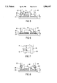
- FIG. 2 shows a hybrid IC comprising a ceramic insulation substrate 1 on which patterns of Ag-Pd alloy conductors 21 and 22 are printed.
- a chip 4 for a semiconductor element is mounted by means of solder 5 through a copper heat sink 3.
- a terminal lead 6 of a covered wire is connected by solder 5 to another thick film conductor 22.
- the semiconductor chip 4 is connected to the terminal lead 6 by soldering an electrode of the semiconductor chip 4 to a connecting conductor 7, which is soldered to the thick film conduct 22.
- FIG. 3 shows another hybrid IC for mounting individual elements.
- a semiconductor element 41 is fixed to the Ag-Pd thick film conductor 21 through the solder 5, and terminal leads 61 and 62 are soldered to the conductors 21 and 22, respectively.
- the sheet resistivity of the Ag-Pd conductor is from 25 to 40 milli-ohm, which is higher than that of the copper foil.
- the width of the Ag-Pd conductor is increased to reduce the resistance, the area occupied by the conductor increases to increase the size. If the thickness of the Ag-Pd conductor is increased the resistance is reduced, but it increases cost since the conductor contains precious metals and printing for the conductor must be made repeatedly.
- An object of the present invention is to obviate the above problems and to provide a highly reliable, small and low cost hybrid IC, wherein in case a circuit element is mounted on a printed circuit board using an Ag-Pd thick film conductor or the like and a large current flows through the thick film conductor, the thick film conductor does not burn.
- the object of the present invention is achieved by a hybrid integrated circuit, which comprises an insulation substrate; a thick film conductor printed and sintered on the insulation substrate; and a circuit part and a terminal conductor brazed on the thick film conductor to constitute the circuit, wherein a connection to the thick film conductor is made through a conductive metal plate brazed on the thick film conductor.
- the circuit part and the terminal conductor are generally directly connected through the conductive metal plate.
- the thick film conductor is preferably made of a silver-palladium alloy, and the metal plate is preferably made of copper. Also, it is preferable that the circuit part is an unsealed semiconductor element, and the metal plate is connected at one end to an electrode disposed on the surface of the unsealed semiconductor element to constitute a part of a conductive member.
- the metal plate may be bent at a portion not brazed to the thick film conductor to constitute a terminal conductor, which preferably has a hole in its end portion.
- the circuit part may be preferably an element with a lead, which is brazed with the metal plate. Also, in case the circuit part is a semiconductor element, it is advantageous to fix on both surfaces thereof metal plates having thermal expansion coefficient similar to that of the semiconductor element.
- the hybrid integrated circuit may further comprise a second thick film conductor printed and sintered on the insulation substrate; a second electrically conductive metal plate brazed on the second thick film conductor; and a second terminal conductor brazed to the second electrically conductive metal plate.
- the circuit part may be an individual element having a lead connected to the second metal plate.
- the second thick film conductor is preferably made of a silver-palladium alloy, and the second metal plate is preferably made of copper. An end of the second metal plate not connected to the second thick film conductor may be bent to constitute a second terminal conductor.
- a good conductive metal plate such as copperplate, the resistance of which is less than 1/25 of the thick film conductor, is fixed, so that most of the current flows through the metal plate. Only several percent of the current flows through the thick film, and heat dissipation from the thick film conductor is reduced to prevent the thick film conductor from rising temperature. Thus, reliability is increased. Also, increase of parts is avoided by commonly employing the metal plate as the terminal lead and the heat sink and by brazing the metal plate directly to an unsealed semiconductor element.
- FIG. 1 is a section view schematically showing a structure of a hybrid IC of a first embodiment of the present invention
- FIG. 2 is a section view schematically showing a structure of a hybrid IC of the prior art
- FIG. 3 is a section view schematically showing a structure of a hybrid IC of the prior art
- FIGS. 4-6 are section views schematically showing structures of second to fourth embodiments of the present invention.
- FIG. 7 is a circuit diagram of the embodiment of the hybrid IC of the present invention.
- FIG. 8 is a section view schematically showing a structure of a fifth embodiment of to the present invention.
- FIGS. 9(a) and 9(b) schematically show a structure of a sixth embodiment of the present invention, in which FIG. 9(a) is a sectional view and FIG. 9(b) is a part of a side view;
- FIGS. 10-13 are section views schematically showing structures of seventh to tenth embodiments of the present invention.
- FIG. 14 is a section view schematically showing a structure of the semiconductor chip and its vicinity in an eleventh embodiment of the present invention.
- FIG. 1 is a sectional view showing an embodiment according to the present invention.
- a bare chip 4 of 10 mm ⁇ 10 mm in an area and 0.25 mm in thickness is fixed by solder 5 to a connecting conductor 7 of a copper strip of 2 mm in width and 0.5 mm in thickness.
- the conductor 7, with the width of 2 mm, is soldered on a thick film conductor 22 of 2 mm in width and 10 mm in length.
- a terminal lead 6 is brazed by solder 5 to the conductor 7.
- FIG. 4 is a sectional view showing the second embodiment according to the present invention.
- a copper plate 81 of 1 mm in thickness is fixed by soldering also on the Ag-Pd thick film conductor 21, and the heat sink 3 is soldered on the copper plate 81.
- a terminal lead 61 is soldered on an end portion of the copper plate 81, which suppresses a current flowing through the thick film conductor 21, so that temperature rise of the thick film conductor 21 is prevented.
- a terminal lead 62 is also soldered on an end portion of the conductor 7.
- FIG. 5 is a sectional view showing the third embodiment according to the present invention.
- a copper plate 81 is bent upwardly at an end portion and is connected to the terminal lead 61 at the end portion.
- the connecting conductor 7 is bent upwardly at an end portion and is connected to the terminal lead 62 at the end portion.
- FIG. 6 is a sectional view showing the fourth embodiment according to the present invention.
- a copper plate 82 is soldered also on the thick film conductor 22, and a lead wire 71 of an individual element 41 like a triac is soldered to the copper plate 82.
- the individual element 41 (the triac element 12) having fine lead wires is connected with low resistance to the input-output lead 62.
- FIG. 8 is a sectional view showing the fifth embodiment according to the present invention.
- end portions of copper plates 81 and 82 are bent upward, and are then connected to the terminal leads 61 and 62 respectively, similar to FIG. 5.
- end portions of the copper plate 81 and the connecting conductor 7 are formed in a shape of the Faston plug terminal, to facilitate connection with an outside device by a contact without employing soldering.
- end portions of the copper plates 81 and 82 are formed in the shape of the Faston plug terminal to connect with an outside device by a contact, as in the embodiment of FIGS. 9(a) and 9(b).
- FIG. 11 is a sectional view showing the eighth embodiment of the hybrid IC of the present invention, which employs the copper plate 82 fixed on the thick film conductor 22 for the bare chip 4 of FIG. 4.
- FIG. 12 is a sectional view showing the ninth embodiment of the present invention, which employs the copper plate 81 as a heat sink and eliminates the heat sink 3 from the hybrid IC of FIG. 4.
- a lower electrode of the chip 4 is soldered to the copper plate 81 through the heat sink 3, similarly to the embodiment of FIG. 5, and the copper plate 81 and the terminal lead 61 are connected to each other in the bent portion of the copper plate 81 by soldering.
- An upper electrode of the chip 4 is connected to the connecting conductor 7 by solder 5.
- One end portion of the connecting conductor 7 is connected to the thick film conductor 22, while the other end portion of the connecting conductor 7 projects upwardly above the chip 4 and is connected to the terminal lead 62.
- FIG. 14 is a sectional view showing the eleventh embodiment of the present invention, which avoids direct connection from the bare chip 4 for a hybrid IC to the heat sink 3 and the connecting conductor 7.
- the bare chip 4 is connected to the heat sink 3 and the connecting conductor 7 through molybdenum plates 9, the thermal expansion coefficient of which is approximately the same as that of the chip 4.
- the employment of the molybdenum plate 9 improves thermal fatigue.
- the thermal fatigue may also be improved by connecting the chip 4 to the copper plate 81 as in the same manner.
- an electrically conductive metal plate is brazed to a thick film conductor with high sheet resistivity to thereby flow most part of an electric current through the metal plate, so that temperature rise of the thick film conductor is prevented and highly reliable hybrid ICs are obtained.
- the width or thickness of the thick film conductor need not be increased and the metal plate can be commonly used as a heat sink or a terminal lead, so that it does not increase cost and size of the hybrid ICs.
Landscapes
- Engineering & Computer Science (AREA)
- Manufacturing & Machinery (AREA)
- Microelectronics & Electronic Packaging (AREA)
- Cooling Or The Like Of Semiconductors Or Solid State Devices (AREA)
- Lead Frames For Integrated Circuits (AREA)
Abstract
Description
Claims (4)
Applications Claiming Priority (2)
| Application Number | Priority Date | Filing Date | Title |
|---|---|---|---|
| JP5142411A JPH0714940A (en) | 1993-06-15 | 1993-06-15 | Hybrid IC |
| JP5-142411 | 1993-06-15 |
Publications (1)
| Publication Number | Publication Date |
|---|---|
| US5506447A true US5506447A (en) | 1996-04-09 |
Family
ID=15314717
Family Applications (1)
| Application Number | Title | Priority Date | Filing Date |
|---|---|---|---|
| US08/257,330 Expired - Fee Related US5506447A (en) | 1993-06-15 | 1994-06-07 | Hybrid integrated circuit |
Country Status (2)
| Country | Link |
|---|---|
| US (1) | US5506447A (en) |
| JP (1) | JPH0714940A (en) |
Cited By (3)
| Publication number | Priority date | Publication date | Assignee | Title |
|---|---|---|---|---|
| US6215185B1 (en) * | 1998-12-11 | 2001-04-10 | Mitsubishi Denki Kabushiki Kaisha | Power semiconductor module |
| US20170338193A1 (en) * | 2014-10-24 | 2017-11-23 | Danfoss Silicon Power Gmbh | Power semiconductor module with short-circuit failure mode |
| US9917031B2 (en) | 2013-09-30 | 2018-03-13 | Fuji Electric Co., Ltd. | Semiconductor device, and method for assembling semiconductor device |
Citations (5)
| Publication number | Priority date | Publication date | Assignee | Title |
|---|---|---|---|---|
| JPS5570056A (en) * | 1978-11-22 | 1980-05-27 | Hitachi Ltd | Preparation of thick film hybrid integrated circuit |
| DD213791A1 (en) * | 1983-02-23 | 1984-09-19 | Inst Regelungstechnik | COMPOUND ELECTRODE FOR CONTACTING ACTIVE SEMICONDUCTOR ELEMENTS |
| JPS6015937A (en) * | 1983-07-07 | 1985-01-26 | Hitachi Cable Ltd | Cladding material for semiconductor support electrode |
| JPS61139054A (en) * | 1984-12-11 | 1986-06-26 | Toshiba Corp | semiconductor equipment |
| JPS6235658A (en) * | 1985-08-09 | 1987-02-16 | Fuji Electric Co Ltd | Semiconductor device |
-
1993
- 1993-06-15 JP JP5142411A patent/JPH0714940A/en active Pending
-
1994
- 1994-06-07 US US08/257,330 patent/US5506447A/en not_active Expired - Fee Related
Patent Citations (5)
| Publication number | Priority date | Publication date | Assignee | Title |
|---|---|---|---|---|
| JPS5570056A (en) * | 1978-11-22 | 1980-05-27 | Hitachi Ltd | Preparation of thick film hybrid integrated circuit |
| DD213791A1 (en) * | 1983-02-23 | 1984-09-19 | Inst Regelungstechnik | COMPOUND ELECTRODE FOR CONTACTING ACTIVE SEMICONDUCTOR ELEMENTS |
| JPS6015937A (en) * | 1983-07-07 | 1985-01-26 | Hitachi Cable Ltd | Cladding material for semiconductor support electrode |
| JPS61139054A (en) * | 1984-12-11 | 1986-06-26 | Toshiba Corp | semiconductor equipment |
| JPS6235658A (en) * | 1985-08-09 | 1987-02-16 | Fuji Electric Co Ltd | Semiconductor device |
Cited By (3)
| Publication number | Priority date | Publication date | Assignee | Title |
|---|---|---|---|---|
| US6215185B1 (en) * | 1998-12-11 | 2001-04-10 | Mitsubishi Denki Kabushiki Kaisha | Power semiconductor module |
| US9917031B2 (en) | 2013-09-30 | 2018-03-13 | Fuji Electric Co., Ltd. | Semiconductor device, and method for assembling semiconductor device |
| US20170338193A1 (en) * | 2014-10-24 | 2017-11-23 | Danfoss Silicon Power Gmbh | Power semiconductor module with short-circuit failure mode |
Also Published As
| Publication number | Publication date |
|---|---|
| JPH0714940A (en) | 1995-01-17 |
Similar Documents
| Publication | Publication Date | Title |
|---|---|---|
| KR900000206B1 (en) | Semiconductor device | |
| CN1299520A (en) | Technology of Wire-bonding Mounting of Integrated Circuit Components to Heat Sinks | |
| US5539618A (en) | Electrical device, in particular switching or controlling device for motor vehicle | |
| US6833997B1 (en) | Combination terminal/leadframe for heat sinking and electrical contacts | |
| JP2001160632A (en) | Thermoelectric module | |
| JP4431756B2 (en) | Resin-sealed semiconductor device | |
| JP2005142189A (en) | Semiconductor device | |
| JP2005045237A (en) | Power semiconductor module with gradeable structure technology | |
| US5506447A (en) | Hybrid integrated circuit | |
| KR19980018524A (en) | Method for manufacturing substrates with at least one metal-laminate and printed boards and their application | |
| US5739743A (en) | Asymmetric resistor terminal | |
| EP0942635B1 (en) | A power semiconductor device for "flip-chip" connections | |
| JPH0777288B2 (en) | Printed circuit board | |
| US5495223A (en) | Hybrid integrated circuit device | |
| CN209929256U (en) | High-current fuse with high-heat-conduction substrate | |
| JP4114902B2 (en) | Composite semiconductor device | |
| US20040055782A1 (en) | Surface-mounting type electronic circuit unit having no melting of solder attaching electric part thereto | |
| JP2703861B2 (en) | Stress-resistant chip component and its mounting method | |
| JP2523389Y2 (en) | PC board device | |
| JPH0325965A (en) | Semiconductor device | |
| JP2867737B2 (en) | Hybrid integrated circuit | |
| JP3012948U (en) | BGA electronic parts | |
| JPH05109919A (en) | Complex integrated circuit | |
| JPH05283147A (en) | Thick-film resistance heating element | |
| JP2002203705A (en) | Resistance heating unit |
Legal Events
| Date | Code | Title | Description |
|---|---|---|---|
| AS | Assignment |
Owner name: FUJI ELECTRIC CO., LTD., JAPAN Free format text: ASSIGNMENT OF ASSIGNORS INTEREST;ASSIGNOR:MURAKAMI, TADAYOSHI;REEL/FRAME:007099/0680 Effective date: 19940708 |
|
| FEPP | Fee payment procedure |
Free format text: PAYOR NUMBER ASSIGNED (ORIGINAL EVENT CODE: ASPN); ENTITY STATUS OF PATENT OWNER: LARGE ENTITY |
|
| FEPP | Fee payment procedure |
Free format text: PAYOR NUMBER ASSIGNED (ORIGINAL EVENT CODE: ASPN); ENTITY STATUS OF PATENT OWNER: LARGE ENTITY Free format text: PAYER NUMBER DE-ASSIGNED (ORIGINAL EVENT CODE: RMPN); ENTITY STATUS OF PATENT OWNER: LARGE ENTITY |
|
| REMI | Maintenance fee reminder mailed | ||
| LAPS | Lapse for failure to pay maintenance fees | ||
| FP | Lapsed due to failure to pay maintenance fee |
Effective date: 20000409 |
|
| STCH | Information on status: patent discontinuation |
Free format text: PATENT EXPIRED DUE TO NONPAYMENT OF MAINTENANCE FEES UNDER 37 CFR 1.362 |