US5488329A - Stabilized voltage generator circuit of the band-gap type - Google Patents
Stabilized voltage generator circuit of the band-gap type Download PDFInfo
- Publication number
- US5488329A US5488329A US08/319,899 US31989994A US5488329A US 5488329 A US5488329 A US 5488329A US 31989994 A US31989994 A US 31989994A US 5488329 A US5488329 A US 5488329A
- Authority
- US
- United States
- Prior art keywords
- transistor
- emitter
- transistors
- circuit
- coupled
- Prior art date
- Legal status (The legal status is an assumption and is not a legal conclusion. Google has not performed a legal analysis and makes no representation as to the accuracy of the status listed.)
- Expired - Fee Related
Links
- 150000001875 compounds Chemical class 0.000 claims description 4
- 230000005669 field effect Effects 0.000 claims description 4
- 230000008878 coupling Effects 0.000 claims description 3
- 238000010168 coupling process Methods 0.000 claims description 3
- 238000005859 coupling reaction Methods 0.000 claims description 3
- 230000008901 benefit Effects 0.000 description 4
- 238000010586 diagram Methods 0.000 description 4
- 230000000694 effects Effects 0.000 description 3
- 238000010276 construction Methods 0.000 description 2
- 230000000875 corresponding effect Effects 0.000 description 2
- 230000001105 regulatory effect Effects 0.000 description 2
- 230000002596 correlated effect Effects 0.000 description 1
- 230000004048 modification Effects 0.000 description 1
- 238000012986 modification Methods 0.000 description 1
Images


Classifications
-
- G—PHYSICS
- G05—CONTROLLING; REGULATING
- G05F—SYSTEMS FOR REGULATING ELECTRIC OR MAGNETIC VARIABLES
- G05F3/00—Non-retroactive systems for regulating electric variables by using an uncontrolled element, or an uncontrolled combination of elements, such element or such combination having self-regulating properties
- G05F3/02—Regulating voltage or current
- G05F3/08—Regulating voltage or current wherein the variable is DC
- G05F3/10—Regulating voltage or current wherein the variable is DC using uncontrolled devices with non-linear characteristics
- G05F3/16—Regulating voltage or current wherein the variable is DC using uncontrolled devices with non-linear characteristics being semiconductor devices
- G05F3/20—Regulating voltage or current wherein the variable is DC using uncontrolled devices with non-linear characteristics being semiconductor devices using diode- transistor combinations
- G05F3/30—Regulators using the difference between the base-emitter voltages of two bipolar transistors operating at different current densities
Definitions
- This invention relates to a voltage generator circuit comprising a cell of the band-gap type, in which a plurality of m parallel-connected transistors form a compound first transistor of a first conductivity type, whose emitter is connected to one end of a first emitter resistor, the other end of this resistor being connected to the emitter of a second transistor of the same conductivity type whose emitter area is equal to that of one of the m transistors forming the compound first transistor, which second transistor has its base coupled to that of the first transistor, the node between the emitter of the second transistor and the first emitter resistor being coupled to a first supply terminal via a second emitter resistor, which circuit further comprises an amplifier acting upon the base of the first and of the second transistor to assure equality of the currents flowing through the first and the second transistor, respectively, the power supply to the collectors of these transistors being received from a second supply terminal.
- a stabilized voltage generator is known particularly from the document EP-A-0,465,094.
- Circuits for the generation of voltages which are independent of temperature and supply voltage variations are very often needed for the construction of modem integrated devices.
- Voltage generator circuits of the band-gap type generally require a supply voltage above 3 forward-biassed junction voltages (3.V BE ) and even 4.V BE .
- a stabilized voltage generator circuit of the type defined in the opening paragraph is characterised, according to the invention, in that the collectors of the first and second transistors are each coupled to the second supply terminal by a first and a second current source, respectively, supplying a current of the same value, in that the amplifier has an input stage comprising two transistors of a conductivity type opposite to that of the first and second transistors and having their emitters, of equivalent area, connected to the collectors of the first and second transistors, respectively, having their bases interconnected and coupled to the first supply terminal via a circuit with a given voltage drop, and having their collectors connected to, respectively, the input and the output of a current mirror of unity ratio, comprising transistors of said first conductivity type and having their emitters coupled to the first supply terminal, in that the amplifier comprises an output stage which is basically formed by a so-called error-amplifier transistor of the first conductivity type, by a so-called bias transistor of the second conductivity type, and by a m-called compensation transistor of the first conductivity type
- V BE which voltage is related to the voltage drop envisaged in the first, the second and the third current source and to the voltage supplied by the circuit having a given voltage drop.
- the circuit known from the above-cited prior-art has a starting circuit comprising four junctions and one field-effect transistor used as a high-value resistor, which elements are disposed in series between the supply terminals.
- the known circuit therefore requires a supply voltage which should be higher than 4.V BE .
- circuit in accordance with the invention can be powered with a voltage of only 2 V, if this is required.
- the circuit in accordance with the invention has a large number of elements operating symmetrically, which provides a high degree of compensation for residual error causes, so that the circuit has an output voltage which is highly stable with respect to temperature variations as well as supply voltage variations.
- the circuit in accordance with the invention also has the feature that it becomes operative as soon as the supply voltage is applied to it.
- the switching device may take various forms, the simplest form being reduced essentially to a field-effect transistor whose control electrode receives a suitable control signal.
- a preferred embodiment of the circuit in accordance with the invention is characterised in that each of the transistors of the current mirror has its emitter coupled to the first supply terminal by means of an emitter resistor of given value, another resistor whose value is equal to half said given value coupling the emitter of the error-amplifier transistor to the same first supply terminal.
- the first and the second current source of the cell are reduced to collector resistors of equal values, while the third current source is formed by another resistor whose value is equal to half that of one of said collector resistors.
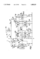
- FIG. 1 is the circuit diagram of an embodiment of the circuit in accordance with the invention.
- FIGS. 2A to 2C are diagrams of different examples of possible arrangements for realising the circuit with a given voltage drop, which forms a part of the generator circuit shown in FIG. 1,
- FIG. 3 shows a first practical example of a switching device which is shown as a block in FIG. 1,
- FIG. 4 shows a second example of this switching device, which also effects a pre-regulation of the supply current of the voltage regulator, and
- FIG. 5 shows the diagram of a third example of a switching device with pre-regulation of the supply current.
- a voltage generator circuit in accordance with the invention comprises a band-gap cell 1 and an amplifier 2 supplying a reference voltage Vref.
- the cell 1 comprises a first transistor T 1 and a second transistor T 2 , the transistor T 1 having an emitter area which is m times as large as the emitter area of the second transistor T 2 .
- the transistor T 1 comprises m separate transistors connected in parallel, which provides a higher accuracy than a configuration comprising a single transistor T 1 .
- the transistor T 1 will be regarded as a single transistor, regardless of its configuration.
- the emitter is connected to a first end of a first emitter resistor 12, whose other end is connected to the emitter of the second transistor T 2 and, via a second emitter resistor 13, to a first supply terminal 9 (ground).
- the bases of the transistors T 1 and T 2 are connected to one another.
- the collector supply for the transistors T 1 and T 2 is received from a second supply terminal 8 via a first collector resistor 14, 15 and a second collector resistor 16, 17, respectively, which resistors serve as paired current sources.
- collector resistors are each shown as two resistor elements in series. For technological reasons it is required, moreover, to provide another resistor whose value is equal to one of these four resistor elements.
- the amplifier 2 has an input stage comprising a pair of PNP-type transistors T 3 , T 4 whose emitters of equal area are connected, respectively, to the collectors of the first and the second transistor T 1 , T 2 .
- the bases of the transistors T 3 and T 4 are interconnected and coupled to the first supply terminal 9 via a circuit 7 which produces a given voltage drop close to or slightly larger than a voltage drop across a forward biassed junction.
- the collector of the transistor T 4 is connected to the input of a current mirror M formed by NPN transistors T 5 and T 6 , the transistor T 5 being connected as a diode and the collector of the transistor T 3 being connected to the collector of the transistor T 6 , the resulting node forming the output of the current mirror.
- the emitters of the transistors T 5 and T 6 are coupled to the first supply terminal 9 via equal resistors 25 and 26, respectively.
- the amplifier comprises an output stage which is essentially formed by an error-amplifier transistor T 56 of the NPN type, a bias transistor T 34 of the PNP type, and a compensation transistor T 22 of the NPN type.
- Each of the transistors forming the output stage is represented as two parallel-connected transistors for the same technological reasons as stated above, i.e. the transistor T 56 has an emitter area equivalent to the combined emitter areas of the transistors T 5 and T 6 , the transistor T 34 has an emitter area equivalent to the combined emitter areas of the transistors T 3 and T 4 , and the transistor T 22 has an emitter area equivalent to twice the emitter area of the transistor T 2 .
- these transistors will be considered as single transistors even if they are formed by two parallel-connected transistors of half the area.
- the node between the collectors of the transistors T 3 and T 6 which forms the output of the input stage, is connected to the base of the error-amplifier transistor T 56 .
- the node between the bases of the two transistors T 3 and T 4 is connected to the base of the bias transistor T 34 and the collectors of the transistors T 34 and T 56 are connected to the node 17' between the bases of the transistors T 1 and T 2 , which node is coupled to the output 18 of the amplifier and to the base of the compensation transistor T 22 .
- the node between the emitter of the bias transistor T 34 and the collector of the compensation transistor T 22 is coupled to the second supply terminal 8 via a resistor 35 whose value is equal to that of one of the resistors 14-17, i.e.
- the resistor 35 thus forms a simple current source supplying a current whose value is twice that of the current through the resistors 14, 15 (or 16, 17).
- the error-amplifier transistor T 56 has its emitter coupled to the first supply terminal 9 via two parallel emitter resistors 45, 46 whose values are equal to one another and which each have a value equal to that of one of the emitter resistors 25 or 26 of the transistors T 5 and T 6 .
- the emitter of the compensation transistor T 22 is coupled to the first supply terminal 9 via a resistor 43 whose value is equal to that of the second emitter resistor 13 of the cell 1.
- a capacitance 19 of low non-critical value may be connected in parallel between the node 17' and the base of the error-amplifier transistor T 56 to provide a better high-frequency stability of the generator circuit.
- the stabilised voltage generator circuit may be used permanently said second supply terminal 8 may be coupled to the positive supply source Vcc.
- the stabilized voltage generator circuit can be turned on or turned off by means of a switching device 11 arranged in series between the actual supply source 10, which is at the positive potential Vcc, and the line referred to as the second supply terminal 8.
- a current I S When a voltage is applied to the supply terminal 8 a current I S will first be divided into two components I 1 and I 2 depending on the collector resistors 14, 15 and the collector resistors 16, 17.
- the current I 1 is divided into a current I A flowing into the emitter of the transistor T 3 and a current I pt flowing into the collector of the transistor T 1 .
- the current I 2 is divided into a current I B flowing into the emitter of the transistor T 4 and a current I pt flowing into the collector of the transistor T 2 .
- the cell is powered in such a way that the collector currents of the transistor T 1 and the transistor T 2 are equal to one another.
- the difference between the currents I A and I B appears on the output of the input stage of the amplifier, i.e. on the node between the collectors of the transistors T 3 and T 6 , which difference is applied to the base of the transistor T 56 .
- the collector current of the transistor T 56 which is an amplified error current, is applied to the node 17' coupling the bases of the transistors T 1 , T 2 , T 22 and provides negative feedback to obtain such a voltage on this node that the currents I pt through the transistors T 1 and T 2 are equal. Since the bases of the transistors T 3 and T 4 are connected to one another and the resistors 14, 15 and 16, 17 are equal to one another, the currents I A and I B are substantially equal.
- the compensation transistor T 22 has an emitter area equal to twice that of the transistor T 2 . Its emitter is connected to an emitter resistor 43 whose value is equal to that of the second emitter resistor 13 of the cell 1, through which a current equal to 2.I pt flows. Likewise, the transistor T 22 also supplies a current which is substantially equal to 2.I pt . Since the resistor 35 is selected to have a value equal to that of one of the resistors 14-17 and the bias transistor T 34 is selected to have an emitter area equal to twice that of one of the transistors T 3 or T 4 , it follows that the current flowing into the emitter of the transistor T 34 is highly equal to 2.I A . Thus, another current of the value I s will flow from the supply terminal 8 into the resistor 35.
- the compensation transistor T 22 in parallel with the transistor T 2 , is adapted to supply a current equal to 2.I pt , bearing in mind that this transistor T 22 has its base coupled to the base of the transistor T 2 and that its collector receives a voltage identical to the collector voltage of the transistor T 2 , the current I s flowing through the resistor 35 being substantially equal to the current I s which is the sum of the currents through the collector resistors 14, 15 and 16, 17.
- V(7)+V BE (T 34 )+R 35 .I s V(7)+V BE (T 34 )+R 35 .I s , where V(7) is the voltage drop in the circuit 7, V BE (T 34 ) is the emitter-base voltage of the transistor T 34 , and R 35 is the value of the resistor 35.
- the voltage drop across the resistor 35 can be chosen to be comparatively small, for example, smaller than 1 V BE but larger than several V T .
- the minimum supply voltage can be slightly higher than 2.V BE and lower than 3V BE , if required.
- a switching device such as the device 11 is arranged between the supply terminal 8 and a source 10 of a voltage Vcc, the voltage of this source can be equal to the voltage defined above or slightly higher if a switching device 11 having an internal resistance is chosen.
- the PNP transistors T 3 , T 4 , T 34 operate with an identical emitter/base voltage and an identical current density.
- the NPN transistors T 1 , T 2 , T 22 operate with the same collector/base voltage and, in addition, the transistors T 2 and T 22 operate with the same current density and the same V BE .
- the transistors T 5 and T 6 operate with identical currents under all conditions because the collector of the transistor T 6 is coupled to the base of the transistor T 56 which operates symmetrically to the combination of the transistors T 5 and T 6 , the transistor T 5 having its collector connected to its base. This provides a completely symmetrical operation for the transistors T 5 , T 6 .
- transistors T 3 and T 4 also operate with an identical collector voltage.
- the node 17' carrying the output voltage Vref, is the only point where a difference occurs with respect to the base voltage of the transistors T 5 and T 6 .
- the value of Vref is of the order of 1.25 V independently of the supply voltage.
- the base/collector voltage of the transistors T 3 and T 4 generally differs from the base/collector voltage of the transistor T 34 although it is easy to achieve voltage equality for a nominal value of the supply voltage.
- the collector current of the transistor T 34 then would have to be slightly smaller or larger than the sum of the collector currents of T 3 and T 4 depending on whether the voltage drop across the resistors 25 and 26 has been selected to be smaller or larger than the voltage drop across the circuit 7, and/or whether the supply voltage differs from its nominal value.
- the effect of the cascode-type configuration of the combination of PNP transistors is that the output resistance of these transistors is multiplied, particularly when a comparatively large voltage drop across the resistors 35, 14-17 is chosen, i.e. distinctly higher than V T .
- FIGS. 2A, 2B and 2C show examples of the block 7 in FIG. 1 which produces a given voltage drop close to or slightly larger than that of a forward biassed junction.
- the value of this voltage drop is selected mainly as a function of the nominal voltage on the second supply terminal 8 and the voltage drops across the resistors 25, 26, 45, 46.
- a preferred value is chosen to ensure that, at the nominal supply voltage, an approximate equality is obtained between the voltage Vref on the node 17' and the voltage of the collectors of the transistors T 3 and T 4 .
- the generator circuit then operates in an optimum manner with a very high degree of symmetry to eliminate most second-order errors.
- the circuit 7 is reduced to a forward-biassed diode-connected bipolar transistor T 7 .
- the bipolar transistor T 7 can be replaced by an N-channel MOS transistor connected in an equivalent manner so as to produce a voltage drop corresponding to its threshold voltage. A voltage drop slightly higher than one V BE is then obtained, whose behaviour as a function of temperature is advantageous for the operation of the generator circuit.
- the circuit 7 takes the form of an arrangement which is known per se, in which a resistor bridge 71, 72 is connected in parallel with the collector-emitter path of an NPN transistor T 70 and whose base is connected to the central node of this resistor bridge.
- This arrangement provides a voltage drop proportional to one V BE , the proportionality factor, which is greater than unity, being selected arbitrarily as a function of the values of the resistors 71 and 72.
- FIG. 2C shows still another example of an arrangement which can be used for the circuit 7 in FIG. 1 and which in the present case is reduced to a resistor bridge 73, 74 connected between the second supply terminal 8 (or the supply source Vcc) and ground (terminal 9).
- the voltage drop used for producing the base current of the transistors T 3 , T 4 and T 34 appears across the resistor 74.
- This voltage drop is influenced by supply voltage variations but this is not unfavourable because the voltage across the resistor 74 varies in the same sense as the variation of the emitter voltage of the transistors T 3 and T 4 .
- the variation of the currents I A and I B as a function of variations of the supply voltage Vcc is then smaller.
- a circuit 7 will be chosen which provides a voltage drop which becomes smaller, and closer to 1 V BE , according as the minimum supply voltage is required to be smaller.
- FIG. 3 shows an example of the switching device 11 in FIG. 1.
- it comprises an enhancement-type P-channel field-effect transistor T 20 having its source connected to the supply source 10 of the voltage Vcc via a resistor 31 and having its drain connected to the second supply terminal 8.
- a control signal is applied to the gate of this transistor T 20 via a terminal 30 to turn on and turn off the transistor under the influence of a control voltage varying between ground potential and the voltage Vcc.
- allowance is to be made for the resistor 31 in series with the source of the transistor T 20 as well as the internal resistance of the transistor. These resistances, disposed in series between the supply source 10 and said second supply terminal 8, produce a voltage drop caused by the current 2.I s .
- FIG. 4 gives another example of the switching device 11 shown in FIG. 1, in which example the current (2.I) supplied to the amplifier 2 in FIG. 1 is pre-regulated.
- an N-channel MOS-FET T 40 has its source connected to the first supply terminal 9 (ground). Its gate receives a suitable control signal from a control terminal 41. Its drain is coupled to the supply source 10 of the voltage V cc via a resistor 42 and a diode-connected PNP-type transistor T 43 .
- Another PNP transistor T 44 has its base connected to the base of the transistor T 43 and has its emitter, whose area is n times as large as that of the emitter of the transistor T 43 , coupled to the source 10 via an emitter resistor 47.
- the collector of the transistor T 44 supplies a current to the second supply terminal 8 whose value, which is given for a nominal voltage Vcc, varies logarithmically and, as a consequence, slightly when Vcc varies.
- circuit shown in FIG. 4 is an equivalent of the circuit shown in FIG. 3, in which the source resistance has a value which varies in the same sense as the value of Vcc, thereby reducing the variations of the voltage produced on the terminal 8.
- FIG. 5 shows a variant of the circuit shown in FIG. 4, in which the transistor T 40 in FIG. 4 is replaced by a PNP type bipolar transistor T 50 whose collector is connected to the terminal 9 (ground) and whose base receives a suitable control signal from the control terminal 51.
- the emitter of the transistor T 50 is coupled to the supply source 10 (Vcc) via a resistor 52 of high value and the base-emitter path of a PNP transistor T 53 .
- a resistor 54 is arranged whose value is selected to produce a voltage drop close to V T under rated operating conditions.
- the collector of the transistor T 53 is connected to the base of another PNP transistor T 55 having its emitter, whose area is n times as large as that of the emitter of the transistor T 53 , connected to the supply source 10.
- the collector of the transistor T 55 supplies a pre-regulated current to the terminal 8, whose value varies little as a function of variations of Vcc around its nominal value, as in the preceding example.
- the circuit in FIG. 4 uses a MOS transistor T 40 for interrupting the power supply while the circuit in FIG. 5 employs a bipolar transistor T 50 to realise the same function.
- MOS transistor T 40 for interrupting the power supply
- bipolar transistor T 50 to realise the same function.
- the expert will easily recognise that the use of transistors of these types could have been interchanged and is in no way specific of each of the examples described, where likewise an NPN type transistor could have been used.
Landscapes
- Engineering & Computer Science (AREA)
- Microelectronics & Electronic Packaging (AREA)
- Physics & Mathematics (AREA)
- Power Engineering (AREA)
- Nonlinear Science (AREA)
- Electromagnetism (AREA)
- General Physics & Mathematics (AREA)
- Radar, Positioning & Navigation (AREA)
- Automation & Control Theory (AREA)
- Control Of Electrical Variables (AREA)
- Amplifiers (AREA)
Applications Claiming Priority (2)
| Application Number | Priority Date | Filing Date | Title |
|---|---|---|---|
| FR9312187 | 1993-10-13 | ||
| FR9312187A FR2711258A1 (fr) | 1993-10-13 | 1993-10-13 | Circuit générateur de tension stabilisée du type bandgap. |
Publications (1)
| Publication Number | Publication Date |
|---|---|
| US5488329A true US5488329A (en) | 1996-01-30 |
Family
ID=9451790
Family Applications (1)
| Application Number | Title | Priority Date | Filing Date |
|---|---|---|---|
| US08/319,899 Expired - Fee Related US5488329A (en) | 1993-10-13 | 1994-10-07 | Stabilized voltage generator circuit of the band-gap type |
Country Status (5)
| Country | Link |
|---|---|
| US (1) | US5488329A (de) |
| EP (1) | EP0649079B1 (de) |
| JP (1) | JPH07152445A (de) |
| DE (1) | DE69413489T2 (de) |
| FR (1) | FR2711258A1 (de) |
Cited By (13)
| Publication number | Priority date | Publication date | Assignee | Title |
|---|---|---|---|---|
| US5627461A (en) * | 1993-12-08 | 1997-05-06 | Nec Corporation | Reference current circuit capable of preventing occurrence of a difference collector current which is caused by early voltage effect |
| US5751182A (en) * | 1996-08-28 | 1998-05-12 | Texas Instruments Incorporated | Rapid start-up circuit for voltage reference and method of operation |
| US5801582A (en) * | 1996-05-24 | 1998-09-01 | Siemens Aktiengesellschaft | Activatable/deactivatable circuit arrangement for producing a reference potential |
| EP0864957A3 (de) * | 1997-02-14 | 1999-03-31 | Canon Kabushiki Kaisha | Schaltung mit konstanten Spannungsausgang |
| US5910749A (en) * | 1995-10-31 | 1999-06-08 | Nec Corporation | Current reference circuit with substantially no temperature dependence |
| US5969566A (en) * | 1996-06-20 | 1999-10-19 | Siemens Aktiengesellschaft | Circuit configuration for generating a reference potential |
| US6211481B1 (en) * | 1998-06-10 | 2001-04-03 | Sodick Co., Ltd. | Power supply device for electric discharge machining apparatus |
| US20050218879A1 (en) * | 2004-03-31 | 2005-10-06 | Silicon Laboratories, Inc. | Voltage reference generator circuit using low-beta effect of a CMOS bipolar transistor |
| US20050285666A1 (en) * | 2004-06-25 | 2005-12-29 | Silicon Laboratories Inc. | Voltage reference generator circuit subtracting CTAT current from PTAT current |
| US20080164567A1 (en) * | 2007-01-09 | 2008-07-10 | Motorola, Inc. | Band gap reference supply using nanotubes |
| CN102591401A (zh) * | 2012-03-16 | 2012-07-18 | 北京经纬恒润科技有限公司 | 内建数字电源电路 |
| US9983614B1 (en) | 2016-11-29 | 2018-05-29 | Nxp Usa, Inc. | Voltage reference circuit |
| US10139849B2 (en) * | 2017-04-25 | 2018-11-27 | Honeywell International Inc. | Simple CMOS threshold voltage extraction circuit |
Families Citing this family (1)
| Publication number | Priority date | Publication date | Assignee | Title |
|---|---|---|---|---|
| CN118426534B (zh) * | 2024-07-05 | 2024-09-24 | 强华时代(成都)科技有限公司 | 无运放带隙基准源电路 |
Citations (3)
| Publication number | Priority date | Publication date | Assignee | Title |
|---|---|---|---|---|
| US4380706A (en) * | 1980-12-24 | 1983-04-19 | Motorola, Inc. | Voltage reference circuit |
| US4945260A (en) * | 1989-04-17 | 1990-07-31 | Advanced Micro Devices, Inc. | Temperature and supply compensated ECL bandgap reference voltage generator |
| EP0465094A2 (de) * | 1990-07-02 | 1992-01-08 | Motorola, Inc. | Bandlückenspannungsreferenz unter Benutzung einer versorgungsunabhängigen Stromquelle |
Family Cites Families (3)
| Publication number | Priority date | Publication date | Assignee | Title |
|---|---|---|---|---|
| US3617859A (en) * | 1970-03-23 | 1971-11-02 | Nat Semiconductor Corp | Electrical regulator apparatus including a zero temperature coefficient voltage reference circuit |
| US4435678A (en) * | 1982-02-26 | 1984-03-06 | Motorola, Inc. | Low voltage precision current source |
| US4524318A (en) * | 1984-05-25 | 1985-06-18 | Burr-Brown Corporation | Band gap voltage reference circuit |
-
1993
- 1993-10-13 FR FR9312187A patent/FR2711258A1/fr not_active Withdrawn
-
1994
- 1994-10-05 DE DE69413489T patent/DE69413489T2/de not_active Expired - Fee Related
- 1994-10-05 EP EP94202878A patent/EP0649079B1/de not_active Expired - Lifetime
- 1994-10-07 US US08/319,899 patent/US5488329A/en not_active Expired - Fee Related
- 1994-10-11 JP JP6245472A patent/JPH07152445A/ja active Pending
Patent Citations (3)
| Publication number | Priority date | Publication date | Assignee | Title |
|---|---|---|---|---|
| US4380706A (en) * | 1980-12-24 | 1983-04-19 | Motorola, Inc. | Voltage reference circuit |
| US4945260A (en) * | 1989-04-17 | 1990-07-31 | Advanced Micro Devices, Inc. | Temperature and supply compensated ECL bandgap reference voltage generator |
| EP0465094A2 (de) * | 1990-07-02 | 1992-01-08 | Motorola, Inc. | Bandlückenspannungsreferenz unter Benutzung einer versorgungsunabhängigen Stromquelle |
Cited By (16)
| Publication number | Priority date | Publication date | Assignee | Title |
|---|---|---|---|---|
| US5627461A (en) * | 1993-12-08 | 1997-05-06 | Nec Corporation | Reference current circuit capable of preventing occurrence of a difference collector current which is caused by early voltage effect |
| US5910749A (en) * | 1995-10-31 | 1999-06-08 | Nec Corporation | Current reference circuit with substantially no temperature dependence |
| US5801582A (en) * | 1996-05-24 | 1998-09-01 | Siemens Aktiengesellschaft | Activatable/deactivatable circuit arrangement for producing a reference potential |
| US5969566A (en) * | 1996-06-20 | 1999-10-19 | Siemens Aktiengesellschaft | Circuit configuration for generating a reference potential |
| US5751182A (en) * | 1996-08-28 | 1998-05-12 | Texas Instruments Incorporated | Rapid start-up circuit for voltage reference and method of operation |
| EP0864957A3 (de) * | 1997-02-14 | 1999-03-31 | Canon Kabushiki Kaisha | Schaltung mit konstanten Spannungsausgang |
| US6211481B1 (en) * | 1998-06-10 | 2001-04-03 | Sodick Co., Ltd. | Power supply device for electric discharge machining apparatus |
| US7321225B2 (en) | 2004-03-31 | 2008-01-22 | Silicon Laboratories Inc. | Voltage reference generator circuit using low-beta effect of a CMOS bipolar transistor |
| US20050218879A1 (en) * | 2004-03-31 | 2005-10-06 | Silicon Laboratories, Inc. | Voltage reference generator circuit using low-beta effect of a CMOS bipolar transistor |
| US20050285666A1 (en) * | 2004-06-25 | 2005-12-29 | Silicon Laboratories Inc. | Voltage reference generator circuit subtracting CTAT current from PTAT current |
| US7224210B2 (en) | 2004-06-25 | 2007-05-29 | Silicon Laboratories Inc. | Voltage reference generator circuit subtracting CTAT current from PTAT current |
| US20080164567A1 (en) * | 2007-01-09 | 2008-07-10 | Motorola, Inc. | Band gap reference supply using nanotubes |
| CN102591401A (zh) * | 2012-03-16 | 2012-07-18 | 北京经纬恒润科技有限公司 | 内建数字电源电路 |
| US9983614B1 (en) | 2016-11-29 | 2018-05-29 | Nxp Usa, Inc. | Voltage reference circuit |
| EP3327538A1 (de) * | 2016-11-29 | 2018-05-30 | NXP USA, Inc. | Spannungsreferenzschaltung |
| US10139849B2 (en) * | 2017-04-25 | 2018-11-27 | Honeywell International Inc. | Simple CMOS threshold voltage extraction circuit |
Also Published As
| Publication number | Publication date |
|---|---|
| EP0649079A1 (de) | 1995-04-19 |
| FR2711258A1 (fr) | 1995-04-21 |
| JPH07152445A (ja) | 1995-06-16 |
| DE69413489D1 (de) | 1998-10-29 |
| EP0649079B1 (de) | 1998-09-23 |
| DE69413489T2 (de) | 1999-05-20 |
Similar Documents
| Publication | Publication Date | Title |
|---|---|---|
| JP3759513B2 (ja) | バンドギャップ基準回路 | |
| US6150872A (en) | CMOS bandgap voltage reference | |
| US4928056A (en) | Stabilized low dropout voltage regulator circuit | |
| US5646518A (en) | PTAT current source | |
| JP3190943B2 (ja) | バイポーラ/cmosレギュレータ回路 | |
| US4626770A (en) | NPN band gap voltage reference | |
| US7902912B2 (en) | Bias current generator | |
| US6384586B1 (en) | Regulated low-voltage generation circuit | |
| US4435678A (en) | Low voltage precision current source | |
| JPS58502170A (ja) | 精密電流源 | |
| US4906863A (en) | Wide range power supply BiCMOS band-gap reference voltage circuit | |
| US4524318A (en) | Band gap voltage reference circuit | |
| US5635869A (en) | Current reference circuit | |
| US4591804A (en) | Cascode current-source arrangement having dual current paths | |
| US4339677A (en) | Electrically variable impedance circuit with feedback compensation | |
| JPH07271461A (ja) | 安定化電圧発生制御回路 | |
| JPH07152445A (ja) | 電圧発生回路 | |
| US6586987B2 (en) | Circuit with source follower output stage and adaptive current mirror bias | |
| US4441070A (en) | Voltage regulator circuit with supply voltage ripple rejection to transient spikes | |
| US6570437B2 (en) | Bandgap reference voltage circuit | |
| US4413226A (en) | Voltage regulator circuit | |
| US4571536A (en) | Semiconductor voltage supply circuit having constant output voltage characteristic | |
| US5410242A (en) | Capacitor and resistor connection in low voltage current source for splitting poles | |
| US4577119A (en) | Trimless bandgap reference voltage generator | |
| US5592123A (en) | Frequency stability bootstrapped current mirror |
Legal Events
| Date | Code | Title | Description |
|---|---|---|---|
| AS | Assignment |
Owner name: U.S. PHILIPS CORPORATION, NEW YORK Free format text: ASSIGNMENT OF ASSIGNORS INTEREST;ASSIGNOR:RIDGERS, TIMOTHY;REEL/FRAME:007184/0539 Effective date: 19940920 |
|
| FPAY | Fee payment |
Year of fee payment: 4 |
|
| REMI | Maintenance fee reminder mailed | ||
| LAPS | Lapse for failure to pay maintenance fees | ||
| FP | Lapsed due to failure to pay maintenance fee |
Effective date: 20040130 |
|
| STCH | Information on status: patent discontinuation |
Free format text: PATENT EXPIRED DUE TO NONPAYMENT OF MAINTENANCE FEES UNDER 37 CFR 1.362 |