US5462896A - Method of forming a sidewall on a semiconductor element - Google Patents
Method of forming a sidewall on a semiconductor element Download PDFInfo
- Publication number
- US5462896A US5462896A US07/903,465 US90346592A US5462896A US 5462896 A US5462896 A US 5462896A US 90346592 A US90346592 A US 90346592A US 5462896 A US5462896 A US 5462896A
- Authority
- US
- United States
- Prior art keywords
- gas
- etching
- sidewall
- silicon
- reactive ion
- Prior art date
- Legal status (The legal status is an assumption and is not a legal conclusion. Google has not performed a legal analysis and makes no representation as to the accuracy of the status listed.)
- Expired - Lifetime
Links
Images


Classifications
-
- H—ELECTRICITY
- H10—SEMICONDUCTOR DEVICES; ELECTRIC SOLID-STATE DEVICES NOT OTHERWISE PROVIDED FOR
- H10D—INORGANIC ELECTRIC SEMICONDUCTOR DEVICES
- H10D30/00—Field-effect transistors [FET]
- H10D30/01—Manufacture or treatment
- H10D30/021—Manufacture or treatment of FETs having insulated gates [IGFET]
- H10D30/028—Manufacture or treatment of FETs having insulated gates [IGFET] of double-diffused metal oxide semiconductor [DMOS] FETs
- H10D30/0291—Manufacture or treatment of FETs having insulated gates [IGFET] of double-diffused metal oxide semiconductor [DMOS] FETs of vertical DMOS [VDMOS] FETs
- H10D30/0293—Manufacture or treatment of FETs having insulated gates [IGFET] of double-diffused metal oxide semiconductor [DMOS] FETs of vertical DMOS [VDMOS] FETs using formation of insulating sidewall spacers
-
- H—ELECTRICITY
- H10—SEMICONDUCTOR DEVICES; ELECTRIC SOLID-STATE DEVICES NOT OTHERWISE PROVIDED FOR
- H10D—INORGANIC ELECTRIC SEMICONDUCTOR DEVICES
- H10D30/00—Field-effect transistors [FET]
- H10D30/01—Manufacture or treatment
- H10D30/021—Manufacture or treatment of FETs having insulated gates [IGFET]
- H10D30/028—Manufacture or treatment of FETs having insulated gates [IGFET] of double-diffused metal oxide semiconductor [DMOS] FETs
- H10D30/0291—Manufacture or treatment of FETs having insulated gates [IGFET] of double-diffused metal oxide semiconductor [DMOS] FETs of vertical DMOS [VDMOS] FETs
-
- H—ELECTRICITY
- H10—SEMICONDUCTOR DEVICES; ELECTRIC SOLID-STATE DEVICES NOT OTHERWISE PROVIDED FOR
- H10D—INORGANIC ELECTRIC SEMICONDUCTOR DEVICES
- H10D30/00—Field-effect transistors [FET]
- H10D30/60—Insulated-gate field-effect transistors [IGFET]
- H10D30/64—Double-diffused metal-oxide semiconductor [DMOS] FETs
- H10D30/66—Vertical DMOS [VDMOS] FETs
- H10D30/665—Vertical DMOS [VDMOS] FETs having edge termination structures
-
- H10P50/283—
-
- H—ELECTRICITY
- H10—SEMICONDUCTOR DEVICES; ELECTRIC SOLID-STATE DEVICES NOT OTHERWISE PROVIDED FOR
- H10D—INORGANIC ELECTRIC SEMICONDUCTOR DEVICES
- H10D62/00—Semiconductor bodies, or regions thereof, of devices having potential barriers
- H10D62/10—Shapes, relative sizes or dispositions of the regions of the semiconductor bodies; Shapes of the semiconductor bodies
- H10D62/102—Constructional design considerations for preventing surface leakage or controlling electric field concentration
- H10D62/103—Constructional design considerations for preventing surface leakage or controlling electric field concentration for increasing or controlling the breakdown voltage of reverse-biased devices
- H10D62/105—Constructional design considerations for preventing surface leakage or controlling electric field concentration for increasing or controlling the breakdown voltage of reverse-biased devices by having particular doping profiles, shapes or arrangements of PN junctions; by having supplementary regions, e.g. junction termination extension [JTE]
-
- H—ELECTRICITY
- H10—SEMICONDUCTOR DEVICES; ELECTRIC SOLID-STATE DEVICES NOT OTHERWISE PROVIDED FOR
- H10D—INORGANIC ELECTRIC SEMICONDUCTOR DEVICES
- H10D62/00—Semiconductor bodies, or regions thereof, of devices having potential barriers
- H10D62/10—Shapes, relative sizes or dispositions of the regions of the semiconductor bodies; Shapes of the semiconductor bodies
- H10D62/102—Constructional design considerations for preventing surface leakage or controlling electric field concentration
- H10D62/112—Constructional design considerations for preventing surface leakage or controlling electric field concentration for preventing surface leakage due to surface inversion layers, e.g. by using channel stoppers
-
- H—ELECTRICITY
- H10—SEMICONDUCTOR DEVICES; ELECTRIC SOLID-STATE DEVICES NOT OTHERWISE PROVIDED FOR
- H10D—INORGANIC ELECTRIC SEMICONDUCTOR DEVICES
- H10D62/00—Semiconductor bodies, or regions thereof, of devices having potential barriers
- H10D62/10—Shapes, relative sizes or dispositions of the regions of the semiconductor bodies; Shapes of the semiconductor bodies
- H10D62/17—Semiconductor regions connected to electrodes not carrying current to be rectified, amplified or switched, e.g. channel regions
- H10D62/393—Body regions of DMOS transistors or IGBTs
-
- H—ELECTRICITY
- H10—SEMICONDUCTOR DEVICES; ELECTRIC SOLID-STATE DEVICES NOT OTHERWISE PROVIDED FOR
- H10D—INORGANIC ELECTRIC SEMICONDUCTOR DEVICES
- H10D64/00—Electrodes of devices having potential barriers
- H10D64/111—Field plates
-
- H—ELECTRICITY
- H10—SEMICONDUCTOR DEVICES; ELECTRIC SOLID-STATE DEVICES NOT OTHERWISE PROVIDED FOR
- H10D—INORGANIC ELECTRIC SEMICONDUCTOR DEVICES
- H10D64/00—Electrodes of devices having potential barriers
- H10D64/20—Electrodes characterised by their shapes, relative sizes or dispositions
- H10D64/27—Electrodes not carrying the current to be rectified, amplified, oscillated or switched, e.g. gates
- H10D64/311—Gate electrodes for field-effect devices
- H10D64/411—Gate electrodes for field-effect devices for FETs
- H10D64/511—Gate electrodes for field-effect devices for FETs for IGFETs
- H10D64/514—Gate electrodes for field-effect devices for FETs for IGFETs characterised by the insulating layers
- H10D64/516—Gate electrodes for field-effect devices for FETs for IGFETs characterised by the insulating layers the thicknesses being non-uniform
Definitions
- the present invention relates to a method of forming sidewalls around a gate electrode material of a semiconductor element.
- U.S. Pat. No. 4,879,254 discloses a fine technique of forming a sidewall at each side of an insulation layer of a semiconductor device by reactive ion etching and forming a transmission path by self-alignment with the insulation layer and sidewall as masks.
- Japanese Unexamined Patent Publication No. 2-86136 discloses a technique of forming, in a semiconductor device, a sidewall of about 1 ⁇ m thick by controlling the thickness of an insulation film to 2 to 3 ⁇ m and the side wall angle of a polysilicon gate electrode material to 80 to 90 degrees while minimizing an over-etching quantity.
- the insulation film used for forming the sidewall is very thick at 2 to 3 ⁇ m, and the sidewall angle must be restricted to 80 to 90 degrees.
- the thick insulation film needs a long over-etching time when forming the sidewall, so that it is very difficult to minimize an etching effect of part that must not be etched. Accordingly, this technique has no practical use.
- An object of the invention is to provide a method of fabricating a semiconductor device having a wide sidewall formed from an insulation film at each side of a gate electrode.
- a first aspect of the invention basically comprises a step of depositing silicon (Si)-based insulation material over a substrate and a step of etching the silicon-based insulation material by a magnetron enhanced reactive ion etching apparatus while pouring carbon-fluoride (CF)-based gas containing hydrogen (H) atoms and a nitrogen (N) or helium (He) gas onto the etched material.
- Si silicon
- CF carbon-fluoride
- a second aspect of the invention basically comprises a first step of forming gate electrode material on an insulation film in a predetermined region on a semiconductor substrate, a second step of forming an insulation film having a predetermined thickness over the gate electrode material on the semiconductor substrate, and a third step of etching the insulation film by a magnetron enhanced reactive ion etching apparatus while pouring a mixture of a CF-based gas and an H 2 gas or a gas mainly made of carbon, coupled by hydrogen and fluorine, and an N 2 or He gas onto the insulation film, such that the insulation film is left at each side of the gate electrode material.
- FIG. 1 is a sectional view showing a semiconductor device according to an embodiment of the invention
- FIGS. 2 through 15 are views showing fabricating processes of the semiconductor device
- FIG. 16 is a view showing a magnetron enhanced reactive ion etching apparatus
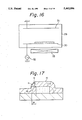
- FIG. 17 is a sectional view showing a semiconductor device and an explanation of an etching process
- FIG. 18 is a graph showing relationships between insulation film thicknesses and sidewall sizes
- FIG. 19 is a graph showing relationships between insulation film thicknesses and sidewall sizes
- FIG. 20 is a graph showing sidewall sizes with and without a magnet
- FIG. 21 is a graph showing relationships between the numbers of processed wafers and etching rates and uniformity of the etching rates
- FIG. 22 is a graph showing relationships between the numbers of processed wafers and etching rates and uniformity of the etching rates
- FIG. 23 is a graph showing relationships between cell sizes and ON resistance values.
- FIG. 24 is a sectional view showing a semiconductor device and an etching process.
- a method of fabricating a semiconductor device basically comprises a step of depositing silicon (Si)-based insulation material over a substrate and a step of etching the silicon-based insulation material by a magnetron enhanced reactive ion etching apparatus while pouring carbon-fluoride (CF)-based gas containing hydrogen (H) atoms and a nitrogen (N) or helium (He) gas onto the etched material.
- Si silicon
- CF carbon-fluoride
- This method improves the decomposing efficiency of the reactive gases and effective depositing reaction products, to form a large tapered portion from the insulation material at each side of the etched portion.
- the tapered portion may optionally be shaped by adjusting etching conditions.
- the tapered portion formed at each side of the etched portion according to the invention serves as a large contact area having no acute curve, to improve wiring efficiency and avoid peeling.
- the inventors have studied various etching conditions on silicon (Si)-based insulation material and found a preferable method of etching the silicon-based insulation material by using a magnetron type reactive ion etching apparatus while pouring a mixture of a carbon-fluoride-based gas containing hydrogen atoms and a nitrogen or helium gas onto the etched material.
- the invention employs the magnetron enhanced reactive ion etching apparatus and the mixed gas, to produce high-concentration plasma that improves the decomposing efficiency of the reactive gas.
- the carbon-fluoride-based gas containing hydrogen atoms function to effectively etch the silicon-based insulation material.
- the nitrogen or helium gas reacts in a gas phase to easily deposit reaction products decomposed by etching over the silicon-based insulation material.
- the nitrogen or helium gas functions to reduce the influence of radicals mainly related to lateral etching, to thereby promote lateral deposition of reaction products at etched portions.
- the reaction products are deposited at the side of the etched portion, the deposited products serve as masks against etching of ion shocks, to laterally move a part to be etched, thereby forming a tapered portion.
- an oxygen gas or a compound gas containing oxygen may be poured during the etching process.
- the invention method etches the silicon-based insulation material formed over the substrate by using a proper mask and forms a tapered portion at the periphery of an opening of the mask.
- the invention is applicable when the substrate on which the silicon-based insulation film is formed has stepped portions such as gate electrodes.
- the silicon-based insulation film may be wholly etched with no mask, to form a tapered portion at each side of the stepped portions such as the gate electrodes.
- a second aspect of the invention basically comprises a first step of forming gate electrode material on an insulation film in a predetermined region on a semiconductor substrate, a second step of forming an insulation film having a predetermined thickness over the gate electrode material on the semiconductor substrate, and a third step of etching the insulation film by a magnetron enhanced reactive ion etching apparatus while pouring a mixture of a carbon-fluoride-based gas and an H 2 gas, or a gas (for example, CHF 3 ) made by coupling carbon, hydrogen, and fluorine while pouring an N 2 or He gas onto the insulation film.
- a magnetron enhanced reactive ion etching apparatus while pouring a mixture of a carbon-fluoride-based gas and an H 2 gas, or a gas (for example, CHF 3 ) made by coupling carbon, hydrogen, and fluorine while pouring an N 2 or He gas onto the insulation film.
- an insulation film 35 formed over a gate electrode material 34 is etched by a magnetron enhanced reactive ion etching apparatus.
- a magnetron discharge generates plasma that easily produces carbon fluoride (CF 2 *, the mark "*" indicating a radical) as follows: ##STR1## This reaction efficiently produces polymer C x F y .
- Adding an N 2 or He gas stabilizes the production of the polymer.
- a competitive reaction between the polymer deposition and the etching determines etching direction (indicated with ⁇ in FIG. 24) and the size W of a sidewall 36.
- the magnetron discharge and the addition of N 2 or He gas promote the reaction of the formula (1), to reduce the etching angle ⁇ and increase the width W of the sidewall 36 relative to the height H of the gate electrode 34.
- CF 2 * of the formula (1) reacts with the oxygen gas or the compound gas containing oxygen as follows:
- FIG. 1 shows a semiconductor device involving an n-channel vertical DMOS transistor zone Z1, a field plate zone Z2, and a peripheral zone (EQR zone) Z3.
- FIGS. 2 through 15 show fabricating processes of this semiconductor device.
- an n + silicon substrate 1 is prepared.
- An n - epitaxial layer 2 is formed over the silicon substrate 1.
- a silicon oxide film 3 of about 3000 to 5000 angstroms thick is formed over the epitaxial layer 2.
- a resist 4 is used to photo-etch the silicon oxide film 3, so as to form deep p - wells.
- boron ions of 3 ⁇ 10 13 cm -2 dose are implanted at about 60 keV, and a drive-in is carried out at 1170 degrees centigrade for 4 to 6 hours under an N 2 atmosphere, to form deep p - well layers 5.
- the silicon oxide film 3 is removed, and a pad oxide film 6 of about 300 to 500 angstroms thick is deposited over the epitaxial layer 2.
- a silicon nitride (Si 3 N 4 ) film 7 of about 1000 to 2000 angstroms thick is deposited over the pad oxide film 6, and by using a resist 8, the silicon nitride film 7 is patterned by photo-etching.
- a field oxide film 9 of about 9000 to 10000 angstroms thick is formed by LOCOS oxidation.
- the silicon nitride film 7 is removed by hot phosphoric acid.
- the pad oxide film 6 is removed by HF etching.
- a gate oxide film 10 of about 300 to 1000 angstroms thick is formed.
- a polysilicon film (11) is entirely deposited by, for example, LPCVD to about 5000 to 10000 angstroms in thickness. Phosphorus is diffused to change the polysilicon film (11) into a phosphorus doped polysilicon film 11.
- the top of the phosphorus doped polysilicon film 11 is thermally oxidized to form a polysilicon oxide film 12 of about 500 to 1500 angstroms thick.
- a silicon oxide film 13 of about 1 ⁇ m thick is formed over the polysilicon oxide film 12.
- the phosphorus doped polysilicon film 11, polysilicon oxide film 12, and silicon oxide film 13 are patterned by photo-etching by using a resist 14.
- a phosphorus doped polysilicon gate electrode material (hereinafter referred to only as the polysilicon gate electrode material) 11a is formed in the transistor forming region through the gate oxide film 10 on the epitaxial layer 2.
- a CVD silicon oxide film 15 of TEOS for properly covering stepped portions is formed to about 1 ⁇ m in thickness.
- the CVD silicon oxide film 15 is etched back to form a sidewall 16 at each side of the phosphorus doped polysilicon film 11 (including the polysilicon gate electrode material 11a).
- the sidewall of the phosphorus doped polysilicon gate electrode material 11a is thermally oxidized after patterning, to form the polysilicon oxide film.
- the sidewall 16 is formed by a magnetron enhanced reactive ion etching apparatus HiRRIE II manufactured by Tokuda Seisakusho.
- FIG. 16 shows this apparatus.
- a chamber 29 incorporates upper and lower electrodes 30 and 31 facing each other.
- the upper electrode 31 is grounded.
- a high-frequency power source 32 supplies the lower electrode 30 with high-frequency electric power of, for example, 500 to 1000 W.
- An electromagnet 33 is disposed under the chamber 29, to form a magnetic field of about 800 gausses.
- the semiconductor substrate of FIG. 9 is placed on the lower electrode 30 of the apparatus.
- the CVD silicon oxide film (sidewall forming insulation film) 15 is etched under, for example, an etching pressure of 6 to 20 Pa, a reactive gas of CHF 3 of 30 to 70 cc/min in flow rate, and an N 2 gas of 10 to 50 cc/min in flow rate, thereby forming the sidewall 16.
- the width W at the bottom of the sidewall 16 is dependent on the film thickness H of a lamination of the phosphorus doped polysilicon film 11, polysilicon oxide film 12, and silicon oxide film 13.
- This width W of the sidewall 16 is smaller than 0.85 times the depth of the n + source region 21 of FIG. 1. Namely, as described in "IEEE Transactions on Electron Devices," February 1980, Vol. ED-27, No. 2, pp. 356 through 367, lateral diffusion is 0.85 times the vertical diffusion, thereby making the width W smaller than 0.85 times the depth of the n + source region 21 to form the n + source region 21 under the polysilicon gate electrode material 11a.
- boron ions of 6 ⁇ 10 13 to 9 ⁇ 10 13 cm -2 dose are implanted into the whole surface at 40 keV without a mask, and a drive-in operation is carried out at 1170 degrees centigrade for about 60 minutes, to form a p - channel region 17.
- a photo-patterned mask 18 is employed to implant phosphorus of 5 ⁇ 10 15 cm -2 dose at 13 keV, to form an n + implanted region 19.
- boron ions of 6 ⁇ 10 -4 cm -2 dose are implanted at about 60 keV into the whole surface, to form a p + implanted region 20, which is used to form body contacts with the p - channel region 17 in the DMOS transistor zone Z1 and contacts in the field plate zone Z2.
- a heat treatment is carried out under an atmosphere of N 2 , to form an n + source region 21 and a p + contact region 22. If the heat treatment is carried out at 1000 to 1050 degrees centigrade for about one hour, the depth of the n + source region and the p + contact region 22 will be about 0.7 to 1.2 ⁇ m. Although the n + source region 21 involves implanted boron ions, the quantity of phosphorus is about 10 times larger than that of boron, so that the boron of this dose has no influence on the n + source region 21.
- a BPSG film 23 is formed over the whole surface. Predetermined regions of the BPSG film 23 are removed by photo-etching (wet or dry etching) by using a resist 24, thereby forming contact holes in the DMOS transistor zone Z1 and field plate zone Z2.
- photo-etching is carried out by using a resist 25, to make contacts with the phosphorus doped polysilicon film 11.
- a resist 25 to make contacts with the phosphorus doped polysilicon film 11.
- holes are made in the peripheral zone (EQR zone) Z3.
- the photo-etching for making the contacts (FIG. 14) in the DMOS transistor zone Z1 and the photo-etching for making the contacts (FIG. 15) in the phosphorus doped polysilicon film 11 are separately carried out because the contacts to the phosphorus doped polysilicon film 11 are thicker than those to the DMOS transistor zone Z1 by the thicknesses of the insulation films (the polysilicon oxide film 12 and silicon oxide film 13), thereby requiring quite different etching conditions.
- phosphorus ions are implanted under the same conditions as for the n + source region 21, to form n + contacts in the peripheral zone (EQR zone) Z3. Annealing is carried out to form an n + layer 26 shown in FIG. 1. Thereafter, an aluminum electrode 27, a passivation film (not shown), and a drain electrode 28 on the back face are formed.
- the polysilicon gate electrode material 11a having a predetermined width is on the gate oxide insulation film 10 formed on the epitaxial layer 2.
- the insulation sidewall 16 having a predetermined width is formed at each side of the electrode material 11a.
- the p - channel region 17 is formed under the polysilicon gate electrode material 11a in the epitaxial layer 2 by implanting boron ions with the electrode material 11a and sidewall 16 as masks.
- the n + source region 21 is formed under the polysilicon gate electrode material 11a in the p - channel region 17 at a depth shallower than the depth of the region 17 and in an area smaller than the region 17 by implanting phosphorus ions with the electrode material 11a and sidewall 16 as masks.
- the polysilicon gate electrode material 11a having a predetermined width is formed on the gate oxide film 10, i.e., the insulation film formed on the epitaxial layer 2, i.e., the semiconductor substrate.
- the p - channel region 17 serving as a first impurity region is positioned under the polysilicon gate electrode material 11a in the epitaxial layer 2.
- the n + source region 21 that is shallower and smaller than the region 17 is positioned under the polysilicon gate electrode material 11a in the p - channel region 17.
- the insulation mask (sidewall) 16 is formed at each side of the polysilicon gate electrode material 11a. The width of the mask (sidewall) 16 is smaller than 0.85 times the depth of the n + source region 21.
- the width W of the sidewall 16 is determined by the horizontal width "a" of the insulation film (CVD silicon oxide film) 15 at the top edge of the gate electrode material 11a and an etching anisotropy (a ratio of vertical to horizontal etching speeds).
- a magnetron discharge easily produces carbon fluoride such as CF 2 as indicated in the formula (1), thereby efficiently producing a polymer having a composition of C x F y (x and y indicating a ratio of C to F), and adding N 2 stably and properly controls the production of the polymer.
- the width W of the sidewall 16 is determined not only by the size "a" of FIG. 17 and the anisotropy but also by a competitive reaction between the polymer deposition and the etching.
- the magnetron discharge and the addition of N 2 gas promote the reaction of the formula (1), reduces the etching angle ⁇ , and widens the width W of the sidewall 16 formed at each side of the gate electrode portion.
- FIG. 18 shows a result of measurement of the widths W of sidewalls and the thicknesses of insulation films (CVD silicon oxide films 15). Conditions of the measurement are shown in Table 1.
- FIG. 18 The prior art shown in FIG. 18 employs a narrow gap apparatus TEL580 for etching, manufactured by Tokyo Electron.
- the prior art requires the silicon oxide film 15 (sidewall forming insulation film) to have a film thickness of 1.8 ⁇ m while the embodiment requires the same to have a film thickness of 1.1 ⁇ m.
- the first step forms the polysilicon gate electrode material 11a over the gate oxide film 10 (insulation film) in a predetermined region on the n - epitaxial layer 2 (semiconductor substrate)
- the second step forms the CVD silicon oxide film 15 (insulation film) having a predetermined thickness on the polysilicon gate electrode material 11a on the n - epitaxial layer 2
- the third step employs the magnetron enhanced reactive ion etching apparatus for etching the CVD silicon oxide film 15 while pouring a CHF 3 gas made by coupling carbon, hydrogen, and fluoride and an N 2 gas onto the etched material, to leave the CVD silicon oxide film 15 only at each side of the polysilicon gate electrode material 11a.
- This technique can broaden the width of the sidewall 16 formed from the CVD silicon oxide film 15 at each side of the gate electrode. Namely, for providing the same size of a sidewall, the CVD silicon oxide film 15 (sidewall forming insulation film) according to the invention will be thinner than that of the prior art, thereby shortening a deposition time of the CVD silicon oxide film 15 and the etching time required to form the sidewall, thereby improving throughput, and reducing costs.
- Power MOS transistors involve deep and wide impurity diffusions Xj (diffusion depths), so that they need sidewalls each of at least 0.5 ⁇ m in width.
- Xj diffusion depths
- each sidewall must be at least 0.5 ⁇ m thick in consideration of withstand voltage and leakage.
- the power MOS transistors must have sidewalls each of at least 0.5 ⁇ m in width W.
- an insulation film for forming the sidewalls must be thick so as to unavoidably increase the quantity of over-etching.
- the thick insulation film results in etching parts such as LOCOS and Si, surfaces of which must not be etched, thereby deteriorating elemental properties. Accordingly, it is practically impossible for the prior art to form sidewalls for the power MOS transistors.
- the embodiment of the invention never raises such problems and is practically useful because it can reduce the thickness of the CVD silicon oxide film 15 (sidewall forming insulation film).
- Tables 2 and 3 show the conditions of the tests, and FIG. 19 shows the results of the tests.
- the first comparison with CF 4 /N 2 , second comparison with CHF 3 /Ar, and third comparison CF 4 /CHF 3 /Ar each provide a small sidewall, which is substantially equal to that of the prior art of Table 1.
- the second embodiment with CF 4 /CHF 3 /N 2 , third embodiment with CHF 3 /He, fourth embodiment with CF 4 /N 2 /H 2 , and fifth embodiment with CHF 3 /He/N 2 /O 2 each show the same effect and the same wide sidewall as the first embodiment with CHF 3 /N 2 .
- FIG. 20 shows measurements of sidewalls prepared with and without a magnet. As shown in the figure, the sidewall prepared without the magnet has a smaller width than that prepared with the magnet.
- the magnet can increase the size of a sidewall owing to highly concentrated plasma produced by the magnet, hydrogen contained as gas components, and added N 2 or He gas.
- the first comparison and fourth embodiment indicate that H 2 is needed to widen the sidewall;
- the first comparison and first embodiment indicate that a gas (CHF 3 ) made by coupling carbon, hydrogen, and fluoride is needed;
- the second embodiment and third comparison indicate that an N 2 gas is needed, and
- the second comparison and third embodiment indicate that an He gas must be poured. Controlling the quantity of an N 2 or He gas in plasma gases controls the production of a polymer and thus the size of each sidewall.
- the fifth embodiment employs gases of CHF 3 , He, N 2 , and O 2 produced by adding O 2 to the gas (CHF 3 /N 2 ) of the first embodiment and the gas (CHF 3 /He) of the third embodiment.
- the addition of the O 2 gas in the fifth embodiment remarkably improves the chamber cleaning cycle.
- FIG. 21 shows the number of processed wafers relative to etching rates and uniformity of the etching rates, in connection with the first embodiment (CHF 3 /N 2 ).
- the first embodiment shows a deterioration in the etching rates and the uniformity of the etching rates around 17 as the number of the processed wafers.
- FIG. 22 shows etching rates and uniformity of the etching rates relative to the number of processed wafers according to the fifth embodiment (CHF 3 /He/N 2 /O 2 ). According to this embodiment, the etching rates and uniformity of the etching rates do not deteriorate even after processing 200 wafers.
- the first embodiment requires the inside of the chamber to be dry- or wet-cleaned after processing 17 wafers, to stabilize processes.
- the fifth embodiment (CHF 3 /He/N 2 /O 2 ) can process at least 200 wafers before cleaning the chamber, thereby greatly improving throughput, because the CF 2 * of the formula (1) stains electrodes of the magnetron enhanced reactive ion etching apparatus, to deteriorate the discharging condition of the apparatus and because the added oxygen gas causes CF 2 * and O 2 to react with each other and form COF 2 * as shown in the formula (2), thereby preventing the electrodes of the magnetron enhanced reactive ion etching apparatus from staining, and thus extending the chamber cleaning cycle.
- CHF 3 /N 2 /O 2 CF 4 /CHF 3 /N 2 /O 2 , or CHF 3 /He/O 2
- a CO 2 gas may be mixed with CHF 3 /N 2
- N 2 O or CO may be added.
- an oxygen gas or a compound gas containing oxygen may be added.
- FIG. 23 shows a relationship between cell size and an ON resistance value per DMOS area. This figure shows that a sidewall can reduce the cell size from 20 ⁇ m square to 15 ⁇ m square with the same withstand voltage. At this time, ON resistance is reduced from 290 m ⁇ .mm 2 to 160 m ⁇ .mm 2 as shown in FIG. 23. It is possible to reduce the cell size to 12 ⁇ m and the ON resistance to less than 160 m ⁇ .mm 2 .
- the sidewall may be widened but a selection ratio of the sidewall forming insulation film and Si may deteriorate.
- the sidewall forming process may be divided into a process of etching and exposing the gate electrode material, etc., and an over-etching process that follows the etching process, as shown in Table 4. Namely, etching conditions may be switched from one to another. This technique stably forms sidewalls.
- the sidewall forming insulation film may be made of SiO 2 as well as BPSG, PSG, SiN, or SiON.
- the invention is applicable for the power MOS transistors as well as any semiconductor integrated circuits, such as DRAMs, that employ sidewalls.
- the gate electrode material may be made of polysilicon as well as aluminum or silicide.
- the gas made by coupling carbon, hydrogen, and fluoride and introduced into the magnetron enhanced reactive ion etching apparatus may be CHF 3 as well as CH 2 F 2 , CH 3 F, or C 2 HF 5 .
- the invention is applicable for etching electrode contact holes, enlarging each sidewall, and tapering the contact holes, thereby providing wiring with stepped portions properly covered.
- the sidewall technique of the invention may be applicable for forming a mask, which is used to form thinner gates.
- the invention provides a novel method of broadening the width of a sidewall made from an insulation film at each side of an etched portion or a gate electrode portion.
- the invention therefore, meets severe requirements of fabricating fine elements, to improve the withstand voltage of the elements and provide stable and simple wiring for the elements.
Landscapes
- Drying Of Semiconductors (AREA)
- Insulated Gate Type Field-Effect Transistor (AREA)
Abstract
A method fabricates a semiconductor device having a sidewall made from an insulation film at each side of a gate electrode portion. The method forms a polysilicon gate electrode (11a) on a gate oxide film (10) in a predetermined region on an n- epitaxial layer (2). A CVD silicon oxide film (15) having a predetermined thickness is formed over the polysilicon gate electrode material (11a) on the n- epitaxial layer (2). A magnetron enhanced reactive ion etching apparatus is used to etch the CVD silicon oxide film (15) while pouring a CHF3 gas made by coupling carbon, hydrogen, and fluorine and an N2 gas onto the etched material, such that the CVD silicon oxide film (15) is left only at each side of the polysilicon gate electrode material (11a), to form a sidewall (16). To avoid electrodes of the magnetron enhanced reactive ion etching apparatus from staining, CHF3/He/N2/O2 may be used for etching.
Description
1. Field of the Invention
The present invention relates to a method of forming sidewalls around a gate electrode material of a semiconductor element.
2. Description of the Related Art
U.S. Pat. No. 4,879,254 discloses a fine technique of forming a sidewall at each side of an insulation layer of a semiconductor device by reactive ion etching and forming a transmission path by self-alignment with the insulation layer and sidewall as masks. Japanese Unexamined Patent Publication No. 2-86136 discloses a technique of forming, in a semiconductor device, a sidewall of about 1 μm thick by controlling the thickness of an insulation film to 2 to 3 μm and the side wall angle of a polysilicon gate electrode material to 80 to 90 degrees while minimizing an over-etching quantity.
According to the latter disclosure, the insulation film used for forming the sidewall is very thick at 2 to 3 μm, and the sidewall angle must be restricted to 80 to 90 degrees. The thick insulation film needs a long over-etching time when forming the sidewall, so that it is very difficult to minimize an etching effect of part that must not be etched. Accordingly, this technique has no practical use.
An object of the invention is to provide a method of fabricating a semiconductor device having a wide sidewall formed from an insulation film at each side of a gate electrode.
In order to accomplish the object, a first aspect of the invention basically comprises a step of depositing silicon (Si)-based insulation material over a substrate and a step of etching the silicon-based insulation material by a magnetron enhanced reactive ion etching apparatus while pouring carbon-fluoride (CF)-based gas containing hydrogen (H) atoms and a nitrogen (N) or helium (He) gas onto the etched material.
A second aspect of the invention basically comprises a first step of forming gate electrode material on an insulation film in a predetermined region on a semiconductor substrate, a second step of forming an insulation film having a predetermined thickness over the gate electrode material on the semiconductor substrate, and a third step of etching the insulation film by a magnetron enhanced reactive ion etching apparatus while pouring a mixture of a CF-based gas and an H2 gas or a gas mainly made of carbon, coupled by hydrogen and fluorine, and an N2 or He gas onto the insulation film, such that the insulation film is left at each side of the gate electrode material.
FIG. 1 is a sectional view showing a semiconductor device according to an embodiment of the invention;
FIGS. 2 through 15 are views showing fabricating processes of the semiconductor device;
FIG. 16 is a view showing a magnetron enhanced reactive ion etching apparatus;
FIG. 17 is a sectional view showing a semiconductor device and an explanation of an etching process;
FIG. 18 is a graph showing relationships between insulation film thicknesses and sidewall sizes;
FIG. 19 is a graph showing relationships between insulation film thicknesses and sidewall sizes;
FIG. 20 is a graph showing sidewall sizes with and without a magnet;
FIG. 21 is a graph showing relationships between the numbers of processed wafers and etching rates and uniformity of the etching rates;
FIG. 22 is a graph showing relationships between the numbers of processed wafers and etching rates and uniformity of the etching rates;
FIG. 23 is a graph showing relationships between cell sizes and ON resistance values; and
FIG. 24 is a sectional view showing a semiconductor device and an etching process.
A method of fabricating a semiconductor device according to the invention basically comprises a step of depositing silicon (Si)-based insulation material over a substrate and a step of etching the silicon-based insulation material by a magnetron enhanced reactive ion etching apparatus while pouring carbon-fluoride (CF)-based gas containing hydrogen (H) atoms and a nitrogen (N) or helium (He) gas onto the etched material.
This method improves the decomposing efficiency of the reactive gases and effective depositing reaction products, to form a large tapered portion from the insulation material at each side of the etched portion. The tapered portion may optionally be shaped by adjusting etching conditions. When forming, for example, aluminum wiring, the tapered portion formed at each side of the etched portion according to the invention serves as a large contact area having no acute curve, to improve wiring efficiency and avoid peeling.
The inventors have studied various etching conditions on silicon (Si)-based insulation material and found a preferable method of etching the silicon-based insulation material by using a magnetron type reactive ion etching apparatus while pouring a mixture of a carbon-fluoride-based gas containing hydrogen atoms and a nitrogen or helium gas onto the etched material.
Namely, the invention employs the magnetron enhanced reactive ion etching apparatus and the mixed gas, to produce high-concentration plasma that improves the decomposing efficiency of the reactive gas. The carbon-fluoride-based gas containing hydrogen atoms function to effectively etch the silicon-based insulation material. The nitrogen or helium gas reacts in a gas phase to easily deposit reaction products decomposed by etching over the silicon-based insulation material.
In a dry etching technique such as that employed by the invention, it is understood that the nitrogen or helium gas functions to reduce the influence of radicals mainly related to lateral etching, to thereby promote lateral deposition of reaction products at etched portions. When the reaction products are deposited at the side of the etched portion, the deposited products serve as masks against etching of ion shocks, to laterally move a part to be etched, thereby forming a tapered portion.
In addition to the mixed gas, an oxygen gas or a compound gas containing oxygen may be poured during the etching process.
The invention method etches the silicon-based insulation material formed over the substrate by using a proper mask and forms a tapered portion at the periphery of an opening of the mask.
The invention is applicable when the substrate on which the silicon-based insulation film is formed has stepped portions such as gate electrodes. In this case, the silicon-based insulation film may be wholly etched with no mask, to form a tapered portion at each side of the stepped portions such as the gate electrodes.
A second aspect of the invention basically comprises a first step of forming gate electrode material on an insulation film in a predetermined region on a semiconductor substrate, a second step of forming an insulation film having a predetermined thickness over the gate electrode material on the semiconductor substrate, and a third step of etching the insulation film by a magnetron enhanced reactive ion etching apparatus while pouring a mixture of a carbon-fluoride-based gas and an H2 gas, or a gas (for example, CHF3) made by coupling carbon, hydrogen, and fluorine while pouring an N2 or He gas onto the insulation film. As a result, the insulation film is left only at each side of the gate electrode material.
The invention will be explained with reference to FIG. 24.
In the figure, an insulation film 35 formed over a gate electrode material 34 is etched by a magnetron enhanced reactive ion etching apparatus. At this time, a magnetron discharge generates plasma that easily produces carbon fluoride (CF2 *, the mark "*" indicating a radical) as follows: ##STR1## This reaction efficiently produces polymer Cx Fy.
Adding an N2 or He gas stabilizes the production of the polymer. A competitive reaction between the polymer deposition and the etching determines etching direction (indicated with θ in FIG. 24) and the size W of a sidewall 36. The magnetron discharge and the addition of N2 or He gas promote the reaction of the formula (1), to reduce the etching angle θ and increase the width W of the sidewall 36 relative to the height H of the gate electrode 34.
When an oxygen gas or a compound gas containing oxygen is added according to the second aspect of the invention, CF2 * of the formula (1) reacts with the oxygen gas or the compound gas containing oxygen as follows:
CF.sub.2 *+1/2O.sub.2 →COF.sub.2 * (2)
This prevents adverse effects on electrodes of the magnetron enhanced reactive ion etching apparatus.
An embodiment of the invention will be explained with reference to the drawings.
FIG. 1 shows a semiconductor device involving an n-channel vertical DMOS transistor zone Z1, a field plate zone Z2, and a peripheral zone (EQR zone) Z3. FIGS. 2 through 15 show fabricating processes of this semiconductor device.
In FIG. 2, an n+ silicon substrate 1 is prepared. An n- epitaxial layer 2 is formed over the silicon substrate 1. A silicon oxide film 3 of about 3000 to 5000 angstroms thick is formed over the epitaxial layer 2.
In FIG. 3, a resist 4 is used to photo-etch the silicon oxide film 3, so as to form deep p- wells.
In FIG. 4, boron ions of 3×1013 cm-2 dose are implanted at about 60 keV, and a drive-in is carried out at 1170 degrees centigrade for 4 to 6 hours under an N2 atmosphere, to form deep p- well layers 5.
In FIG. 5, the silicon oxide film 3 is removed, and a pad oxide film 6 of about 300 to 500 angstroms thick is deposited over the epitaxial layer 2. A silicon nitride (Si3 N4) film 7 of about 1000 to 2000 angstroms thick is deposited over the pad oxide film 6, and by using a resist 8, the silicon nitride film 7 is patterned by photo-etching.
In FIG. 6, a field oxide film 9 of about 9000 to 10000 angstroms thick is formed by LOCOS oxidation. The silicon nitride film 7 is removed by hot phosphoric acid. The pad oxide film 6 is removed by HF etching. A gate oxide film 10 of about 300 to 1000 angstroms thick is formed.
In FIG. 7, a polysilicon film (11) is entirely deposited by, for example, LPCVD to about 5000 to 10000 angstroms in thickness. Phosphorus is diffused to change the polysilicon film (11) into a phosphorus doped polysilicon film 11. The top of the phosphorus doped polysilicon film 11 is thermally oxidized to form a polysilicon oxide film 12 of about 500 to 1500 angstroms thick. A silicon oxide film 13 of about 1 μm thick is formed over the polysilicon oxide film 12.
In FIG. 8, the phosphorus doped polysilicon film 11, polysilicon oxide film 12, and silicon oxide film 13 are patterned by photo-etching by using a resist 14.
As a result, as shown in FIG. 9, a phosphorus doped polysilicon gate electrode material (hereinafter referred to only as the polysilicon gate electrode material) 11a is formed in the transistor forming region through the gate oxide film 10 on the epitaxial layer 2. Thereafter, a CVD silicon oxide film 15 of TEOS for properly covering stepped portions is formed to about 1 μm in thickness.
In FIG. 10, the CVD silicon oxide film 15 is etched back to form a sidewall 16 at each side of the phosphorus doped polysilicon film 11 (including the polysilicon gate electrode material 11a).
In FIG. 9, the sidewall of the phosphorus doped polysilicon gate electrode material 11a is thermally oxidized after patterning, to form the polysilicon oxide film.
The sidewall 16 is formed by a magnetron enhanced reactive ion etching apparatus HiRRIE II manufactured by Tokuda Seisakusho. FIG. 16 shows this apparatus. In the figure, a chamber 29 incorporates upper and lower electrodes 30 and 31 facing each other. The upper electrode 31 is grounded. A high-frequency power source 32 supplies the lower electrode 30 with high-frequency electric power of, for example, 500 to 1000 W. An electromagnet 33 is disposed under the chamber 29, to form a magnetic field of about 800 gausses.
The semiconductor substrate of FIG. 9 is placed on the lower electrode 30 of the apparatus. The CVD silicon oxide film (sidewall forming insulation film) 15 is etched under, for example, an etching pressure of 6 to 20 Pa, a reactive gas of CHF3 of 30 to 70 cc/min in flow rate, and an N2 gas of 10 to 50 cc/min in flow rate, thereby forming the sidewall 16.
The width W at the bottom of the sidewall 16 is dependent on the film thickness H of a lamination of the phosphorus doped polysilicon film 11, polysilicon oxide film 12, and silicon oxide film 13. This width W of the sidewall 16 is smaller than 0.85 times the depth of the n+ source region 21 of FIG. 1. Namely, as described in "IEEE Transactions on Electron Devices," February 1980, Vol. ED-27, No. 2, pp. 356 through 367, lateral diffusion is 0.85 times the vertical diffusion, thereby making the width W smaller than 0.85 times the depth of the n+ source region 21 to form the n+ source region 21 under the polysilicon gate electrode material 11a.
In FIG. 11, boron ions of 6×10¹³ to 9×1013 cm-2 dose are implanted into the whole surface at 40 keV without a mask, and a drive-in operation is carried out at 1170 degrees centigrade for about 60 minutes, to form a p- channel region 17.
In FIG. 12, a photo-patterned mask 18 is employed to implant phosphorus of 5×1015 cm-2 dose at 13 keV, to form an n+ implanted region 19.
In FIG. 13, boron ions of 6×10⁻⁴ cm-2 dose are implanted at about 60 keV into the whole surface, to form a p+ implanted region 20, which is used to form body contacts with the p- channel region 17 in the DMOS transistor zone Z1 and contacts in the field plate zone Z2.
In FIG. 14, a heat treatment is carried out under an atmosphere of N2, to form an n+ source region 21 and a p+ contact region 22. If the heat treatment is carried out at 1000 to 1050 degrees centigrade for about one hour, the depth of the n+ source region and the p+ contact region 22 will be about 0.7 to 1.2 μm. Although the n+ source region 21 involves implanted boron ions, the quantity of phosphorus is about 10 times larger than that of boron, so that the boron of this dose has no influence on the n+ source region 21.
Thereafter, a BPSG film 23 is formed over the whole surface. Predetermined regions of the BPSG film 23 are removed by photo-etching (wet or dry etching) by using a resist 24, thereby forming contact holes in the DMOS transistor zone Z1 and field plate zone Z2.
In FIG. 15, photo-etching is carried out by using a resist 25, to make contacts with the phosphorus doped polysilicon film 11. At the same time, holes are made in the peripheral zone (EQR zone) Z3.
The photo-etching for making the contacts (FIG. 14) in the DMOS transistor zone Z1 and the photo-etching for making the contacts (FIG. 15) in the phosphorus doped polysilicon film 11 are separately carried out because the contacts to the phosphorus doped polysilicon film 11 are thicker than those to the DMOS transistor zone Z1 by the thicknesses of the insulation films (the polysilicon oxide film 12 and silicon oxide film 13), thereby requiring quite different etching conditions.
As shown in FIG. 15, phosphorus ions are implanted under the same conditions as for the n+ source region 21, to form n+ contacts in the peripheral zone (EQR zone) Z3. Annealing is carried out to form an n+ layer 26 shown in FIG. 1. Thereafter, an aluminum electrode 27, a passivation film (not shown), and a drain electrode 28 on the back face are formed.
The semiconductor device with integrated vertical DMOS power transistors is thus completed.
In the semiconductor device formed, the polysilicon gate electrode material 11a having a predetermined width is on the gate oxide insulation film 10 formed on the epitaxial layer 2. The insulation sidewall 16 having a predetermined width is formed at each side of the electrode material 11a. The p- channel region 17 is formed under the polysilicon gate electrode material 11a in the epitaxial layer 2 by implanting boron ions with the electrode material 11a and sidewall 16 as masks. The n+ source region 21 is formed under the polysilicon gate electrode material 11a in the p- channel region 17 at a depth shallower than the depth of the region 17 and in an area smaller than the region 17 by implanting phosphorus ions with the electrode material 11a and sidewall 16 as masks.
As mentioned above, the polysilicon gate electrode material 11a having a predetermined width is formed on the gate oxide film 10, i.e., the insulation film formed on the epitaxial layer 2, i.e., the semiconductor substrate. The p- channel region 17 serving as a first impurity region is positioned under the polysilicon gate electrode material 11a in the epitaxial layer 2. Also, the n+ source region 21 that is shallower and smaller than the region 17 is positioned under the polysilicon gate electrode material 11a in the p- channel region 17. The insulation mask (sidewall) 16 is formed at each side of the polysilicon gate electrode material 11a. The width of the mask (sidewall) 16 is smaller than 0.85 times the depth of the n+ source region 21.
A technique for finely designing this semiconductor device is disclosed in U.S. Pat. No. 5,250,449 by this applicant so that it will not be described here.
Processes of forming the sidewall 16 by using the magnetron enhanced reactive ion etching apparatus while pouring CHF3 gas and N2 gas will be explained in detail.
As shown in FIG. 17, the width W of the sidewall 16 is determined by the horizontal width "a" of the insulation film (CVD silicon oxide film) 15 at the top edge of the gate electrode material 11a and an etching anisotropy (a ratio of vertical to horizontal etching speeds). A magnetron discharge easily produces carbon fluoride such as CF2 as indicated in the formula (1), thereby efficiently producing a polymer having a composition of Cx Fy (x and y indicating a ratio of C to F), and adding N2 stably and properly controls the production of the polymer.
The width W of the sidewall 16 is determined not only by the size "a" of FIG. 17 and the anisotropy but also by a competitive reaction between the polymer deposition and the etching. The magnetron discharge and the addition of N2 gas promote the reaction of the formula (1), reduces the etching angle θ, and widens the width W of the sidewall 16 formed at each side of the gate electrode portion.
FIG. 18 shows a result of measurement of the widths W of sidewalls and the thicknesses of insulation films (CVD silicon oxide films 15). Conditions of the measurement are shown in Table 1.
The prior art shown in FIG. 18 employs a narrow gap apparatus TEL580 for etching, manufactured by Tokyo Electron.
              TABLE 1
______________________________________
           First embodiment
                      Prior art
______________________________________
Flow rate (cc/min)
CF.sub.4     --            40
CHF.sub.3    50            40
N.sub.2      10           --
Ar           --           700
Pressure (Pa)
           13         133
High-frequency power (W)
           600        250
Magnet
           with       without
______________________________________
To make the width W of a sidewall to be 0.7 μm, the prior art requires the silicon oxide film 15 (sidewall forming insulation film) to have a film thickness of 1.8 μm while the embodiment requires the same to have a film thickness of 1.1 μm.
As explained above, according to the embodiment method, the first step forms the polysilicon gate electrode material 11a over the gate oxide film 10 (insulation film) in a predetermined region on the n- epitaxial layer 2 (semiconductor substrate), the second step forms the CVD silicon oxide film 15 (insulation film) having a predetermined thickness on the polysilicon gate electrode material 11a on the n- epitaxial layer 2, and the third step employs the magnetron enhanced reactive ion etching apparatus for etching the CVD silicon oxide film 15 while pouring a CHF3 gas made by coupling carbon, hydrogen, and fluoride and an N2 gas onto the etched material, to leave the CVD silicon oxide film 15 only at each side of the polysilicon gate electrode material 11a.
This technique can broaden the width of the sidewall 16 formed from the CVD silicon oxide film 15 at each side of the gate electrode. Namely, for providing the same size of a sidewall, the CVD silicon oxide film 15 (sidewall forming insulation film) according to the invention will be thinner than that of the prior art, thereby shortening a deposition time of the CVD silicon oxide film 15 and the etching time required to form the sidewall, thereby improving throughput, and reducing costs.
Power MOS transistors involve deep and wide impurity diffusions Xj (diffusion depths), so that they need sidewalls each of at least 0.5 μm in width. When the sidewalls are used as electric insulation and separation layers with self-aligning contacts, each sidewall must be at least 0.5 μm thick in consideration of withstand voltage and leakage.
In this way, the power MOS transistors must have sidewalls each of at least 0.5 μm in width W. According to the prior art, an insulation film for forming the sidewalls must be thick so as to unavoidably increase the quantity of over-etching. The thick insulation film results in etching parts such as LOCOS and Si, surfaces of which must not be etched, thereby deteriorating elemental properties. Accordingly, it is practically impossible for the prior art to form sidewalls for the power MOS transistors. The embodiment of the invention never raises such problems and is practically useful because it can reduce the thickness of the CVD silicon oxide film 15 (sidewall forming insulation film).
Tests have been made with a magnetron enhanced reactive ion etching apparatus and various etching gases. Tables 2 and 3 show the conditions of the tests, and FIG. 19 shows the results of the tests.
              TABLE 2
______________________________________
Embodiments                        Fifth
Second         Third     Fourth    CHF.sub.3 /He/
CF.sub.4 /CHF.sub.3 /N.sub.2
               CHF.sub.3 /He
                         CF.sub.4 /N.sub.2 /H.sub.2
                                   N.sub.2 /O.sub.2
______________________________________
Flow rate (cc/min)
CHF.sub.3
       25          50        --      70
CF.sub.4
       25          --        50      --
N.sub.2
       10          --        10      10
Ar     --          --        --      --
He     --          10        --      15
H.sub.2
       --          --        20      --
O.sub.2
       --          --        --      10
High-frequency power (W)
600            600       600       600
Pressure (Pa)
13             13        13        13
______________________________________
              TABLE 3
______________________________________
Comparison
First            Second    Third
CF.sub.4 /N.sub.2
                 CHF.sub.3 /Ar
                           CF.sub.4 /CHF.sub.3 /Ar
______________________________________
Flow rate (cc/min)
CHF.sub.3
        --           59        25
CF.sub.4
        50           --        25
N.sub.2 10           --        --
Ar      --           10        10
He      --           --        --
H.sub.2 --           --        --
O.sub.2 --           --        --
High-frequency power (W)
600              600       600
Pressure (Pa)
13               13        13
______________________________________
The first comparison with CF4 /N2, second comparison with CHF3 /Ar, and third comparison CF4 /CHF3 /Ar each provide a small sidewall, which is substantially equal to that of the prior art of Table 1.
The second embodiment with CF4 /CHF3 /N2, third embodiment with CHF3 /He, fourth embodiment with CF4 /N2 /H2, and fifth embodiment with CHF3 /He/N2 /O2 each show the same effect and the same wide sidewall as the first embodiment with CHF3 /N2.
FIG. 20 shows measurements of sidewalls prepared with and without a magnet. As shown in the figure, the sidewall prepared without the magnet has a smaller width than that prepared with the magnet.
These tests indicate that the magnet can increase the size of a sidewall owing to highly concentrated plasma produced by the magnet, hydrogen contained as gas components, and added N2 or He gas. Namely, in FIG. 19, the first comparison and fourth embodiment indicate that H2 is needed to widen the sidewall; the first comparison and first embodiment indicate that a gas (CHF3) made by coupling carbon, hydrogen, and fluoride is needed; the second embodiment and third comparison indicate that an N2 gas is needed, and the second comparison and third embodiment indicate that an He gas must be poured. Controlling the quantity of an N2 or He gas in plasma gases controls the production of a polymer and thus the size of each sidewall.
The fifth embodiment employs gases of CHF3, He, N2, and O2 produced by adding O2 to the gas (CHF3 /N2) of the first embodiment and the gas (CHF3 /He) of the third embodiment. The addition of the O2 gas in the fifth embodiment remarkably improves the chamber cleaning cycle.
FIG. 21 shows the number of processed wafers relative to etching rates and uniformity of the etching rates, in connection with the first embodiment (CHF3 /N2). An abscissa of the figure represents the number of processed wafers and an ordinate thereof indicates mean etching rates of many sampling points of the wafers as well as uniformity {=(Vmax-Vmin)/(Vmax+Vmin)} of the etching rates V at the many sampling points of the wafers. The first embodiment shows a deterioration in the etching rates and the uniformity of the etching rates around 17 as the number of the processed wafers.
FIG. 22 shows etching rates and uniformity of the etching rates relative to the number of processed wafers according to the fifth embodiment (CHF3 /He/N2 /O2). According to this embodiment, the etching rates and uniformity of the etching rates do not deteriorate even after processing 200 wafers.
As a result, the first embodiment requires the inside of the chamber to be dry- or wet-cleaned after processing 17 wafers, to stabilize processes. On the other hand, the fifth embodiment (CHF3 /He/N2 /O2) can process at least 200 wafers before cleaning the chamber, thereby greatly improving throughput, because the CF2 * of the formula (1) stains electrodes of the magnetron enhanced reactive ion etching apparatus, to deteriorate the discharging condition of the apparatus and because the added oxygen gas causes CF2 * and O2 to react with each other and form COF2 * as shown in the formula (2), thereby preventing the electrodes of the magnetron enhanced reactive ion etching apparatus from staining, and thus extending the chamber cleaning cycle.
As modifications of the fifth embodiment, CHF3 /N2 /O2, CF4 /CHF3 /N2 /O2, or CHF3 /He/O2 may be used, a CO2 gas may be mixed with CHF3 /N2, and N2 O or CO may be added. Namely, an oxygen gas or a compound gas containing oxygen may be added.
FIG. 23 shows a relationship between cell size and an ON resistance value per DMOS area. This figure shows that a sidewall can reduce the cell size from 20 μm square to 15 μm square with the same withstand voltage. At this time, ON resistance is reduced from 290 mΩ.mm2 to 160 mΩ.mm2 as shown in FIG. 23. It is possible to reduce the cell size to 12 μm and the ON resistance to less than 160 mΩ.mm2.
This invention is not limited to the above embodiments. When N2 is added, the sidewall may be widened but a selection ratio of the sidewall forming insulation film and Si may deteriorate. To deal with this problem, the sidewall forming process may be divided into a process of etching and exposing the gate electrode material, etc., and an over-etching process that follows the etching process, as shown in Table 4. Namely, etching conditions may be switched from one to another. This technique stably forms sidewalls.
              TABLE 4
______________________________________
         First step
                   Second step
         (Main etching)
                   (Over-etching)
______________________________________
Flow rates (cc/min)
CHF.sub.3  25          25
CF.sub.4   25          25
N.sub.2    10          --
Ar         --          10
High-frequency power (W)
         600       600
Pressure (Pa)
         13        13
______________________________________
The sidewall forming insulation film may be made of SiO2 as well as BPSG, PSG, SiN, or SiON. The invention is applicable for the power MOS transistors as well as any semiconductor integrated circuits, such as DRAMs, that employ sidewalls.
The gate electrode material may be made of polysilicon as well as aluminum or silicide.
The gas made by coupling carbon, hydrogen, and fluoride and introduced into the magnetron enhanced reactive ion etching apparatus may be CHF3 as well as CH2 F2, CH3 F, or C2 HF5.
The invention is applicable for etching electrode contact holes, enlarging each sidewall, and tapering the contact holes, thereby providing wiring with stepped portions properly covered. The sidewall technique of the invention may be applicable for forming a mask, which is used to form thinner gates.
As explained above in detail, the invention provides a novel method of broadening the width of a sidewall made from an insulation film at each side of an etched portion or a gate electrode portion. The invention, therefore, meets severe requirements of fabricating fine elements, to improve the withstand voltage of the elements and provide stable and simple wiring for the elements.
Claims (10)
1. A method of fabricating a semiconductor device comprising the steps of:
depositing silicon (Si)-based insulation material over a substrate having stepped portions provided on a main portion of the substrate, said stepped portions each having a height measured from said main surface thereof, wherein on each of the side surfaces of said stepped portions, a side wall portion comprising said silicon (Si)-based insulation material is provided, a laterally extending portion of said side wall portion having a width which is determined in accordance with said height of said stepped portion; and
etching the silicon-based insulation material by a magnetron-enhanced reactive ion-etching apparatus while pouring onto the etched material carbon-fluoride (CF)-based gas mixed with hydrogen (H), nitrogen (N) or helium (He) gas, the nitrogen and helium gas do not directly contribute to said etching operation, and wherein said etching operation is carried out so as to deposit a polymer formed during said etching step on said sidewall to thereby expand said width of said laterally extending portion of said sidewall portion.
2. A method of fabricating a semiconductor device comprising the steps of:
forming on a main surface of a substrate, a plurality of stepped portions, each having a height, measured from said main surface of said substrate;
depositing silicon (Si)-based insulation material over said substrate provided with said stepped portions on said main surface thereof, wherein on each of the side surfaces of said stepped portions, a side wall portion comprising said silicon (Si)-based insulation material is provided, a laterally extending portion of said side wall portion having a width which is determined in accordance with said height of said stepped portion; and
etching the whole surface of the silicon-based insulation material by a magnetron enhanced reactive ion etching apparatus while pouring carbon-fluoride (CF)-based gas containing hydrogen (H) atoms and a nitrogen (N) or helium (He) gas onto the etched material, and wherein said etching operation is carried out so as to deposit a polymer formed during said etching step on said sidewall to thereby expand said width of said laterally extending portion of said sidewall portion.
3. A method according to claim 2, wherein the step of etching the whole surface of the silicon-based insulation material by the magnetron enhanced reactive ion etching apparatus employs at least one processing material selected among a mixture of a carbon-fluoride (CF)-based gas and a hydrogen (H2) gas and a gas made of carbon coupled with hydrogen, and fluorine and at least one gas selected from the group consisting of nitrogen (N) gas and a helium (He) gas.
4. A method according to claim 1, wherein the step of etching the whole surface of the silicon-based insulation material by the magnetron enhanced reactive ion etching apparatus employs at least one processing material selected among a mixture of a carbon-fluoride (CF)-based gas and a hydrogen (H2) gas and a gas made of carbon coupled with hydrogen, and fluorine and at least one gas selected from the group consisting of nitrogen (N) gas and a helium (He) gas.
5. A method according to claim 2, wherein the stepped portions are made of gate electrode forming material.
6. A method according to claim 2, wherein the stepped portions are made of gate electrode forming material.
7. A method according to claim 1, wherein the step of etching the insulation film is conducted while adding an oxygen gas or a compound gas containing oxygen.
8. A method according to claim 2, wherein the step of etching the whole surface of the silicon-based insulation material by the magnetron enhanced reactive ion etching apparatus employs carbon-fluoride (CF)-based gas containing hydrogen (H) atoms and at least one processing material selected from the group consisting of a CF-based+H2 gas and a CHF based gas.
9. A method according to claim 1, wherein the step of etching the insulation film is conducted while adding an oxygen gas or a compound gas containing oxygen.
10. A method according to claim 1, wherein the step of etching the whole surface of the silicon-based insulation material by the magnetron enhanced reactive ion etching apparatus employs carbon-fluoride (CF)-based gas containing hydrogen (H) atoms and at least one processing material selected from the group consisting of a CF-based+H2 gas and a CHF based gas.
Applications Claiming Priority (4)
| Application Number | Priority Date | Filing Date | Title |
|---|---|---|---|
| JP15199391 | 1991-06-24 | ||
| JP3-151993 | 1991-06-24 | ||
| JP3-271430 | 1991-10-18 | ||
| JP27143091A JP3146561B2 (en) | 1991-06-24 | 1991-10-18 | Method for manufacturing semiconductor device |
Publications (1)
| Publication Number | Publication Date |
|---|---|
| US5462896A true US5462896A (en) | 1995-10-31 |
Family
ID=26481047
Family Applications (1)
| Application Number | Title | Priority Date | Filing Date |
|---|---|---|---|
| US07/903,465 Expired - Lifetime US5462896A (en) | 1991-06-24 | 1992-06-23 | Method of forming a sidewall on a semiconductor element |
Country Status (2)
| Country | Link |
|---|---|
| US (1) | US5462896A (en) |
| JP (1) | JP3146561B2 (en) |
Cited By (15)
| Publication number | Priority date | Publication date | Assignee | Title |
|---|---|---|---|---|
| EP0812018A1 (en) * | 1996-06-04 | 1997-12-10 | Siemens Aktiengesellschaft | CMOS-semiconductor device with field plates and self-aligned contact as well as method of manufacturing thereof |
| EP0805485A3 (en) * | 1996-04-29 | 1999-09-01 | Applied Materials, Inc. | Method for plasma etching dielectric layers with high selectivity and low microloading effect |
| WO1999057757A1 (en) * | 1998-05-05 | 1999-11-11 | Lam Research Corporation | Method for etching silicon dioxide using fluorocarbon gas chemistry |
| US5994227A (en) * | 1997-12-24 | 1999-11-30 | Mitsubishi Denki Kabushiki Kaisha | Method of manufacturing semiconductor device |
| US6083844A (en) * | 1997-12-22 | 2000-07-04 | Lam Research Corporation | Techniques for etching an oxide layer |
| WO2000039846A1 (en) * | 1998-12-31 | 2000-07-06 | Lam Research Corporation | Method of etching silicon dioxide using hydrogen-containing additive gases in fluorocarbon gas chemistry |
| EP1085563A3 (en) * | 1999-09-13 | 2001-09-19 | Motorola, Inc. | Process for etching an insulating layer and forming a semiconductor device |
| US6432830B1 (en) | 1998-05-15 | 2002-08-13 | Applied Materials, Inc. | Semiconductor fabrication process |
| US20040074515A1 (en) * | 2002-10-22 | 2004-04-22 | Jung-Wook Kim | Method for cleaning a processing chamber and method for manufacturing a semiconductor device |
| US20040084413A1 (en) * | 1999-01-27 | 2004-05-06 | Matsushita Electric Industrial Co., Ltd. | Etching method |
| US20060081182A1 (en) * | 2004-10-15 | 2006-04-20 | Tokyo Electron Limited | Method of cleaning thin film deposition system, thin film deposition system and program |
| US20090160070A1 (en) * | 2007-12-24 | 2009-06-25 | Dongbu Hitek Co., Ltd. | Metal line in a semiconductor device |
| US20130081263A1 (en) * | 2011-09-30 | 2013-04-04 | Hitachi Global Storage Technologies Netherlands B.V. | Method for manufacturing a magnetic write pole of a perpendicular magnetic write head using novel mask fabrication |
| US8796152B2 (en) * | 2012-12-13 | 2014-08-05 | HGST Netherlands B.V. | Method for manufacturing a magnetoresistive sensor |
| CN107425064A (en) * | 2016-05-23 | 2017-12-01 | 北大方正集团有限公司 | Bilateral wall VDMOS device and preparation method thereof |
Families Citing this family (8)
| Publication number | Priority date | Publication date | Assignee | Title |
|---|---|---|---|---|
| WO2013069070A1 (en) * | 2011-11-11 | 2013-05-16 | パイオニア株式会社 | Semiconductor device and active matrix drive circuit using same |
| USD862844S1 (en) | 2018-08-22 | 2019-10-15 | IFG Cure Holdings, LLC | PPR shirt |
| USD854282S1 (en) | 2018-08-22 | 2019-07-23 | IFG Cure Holdings, LLC | Kinematic shirt back |
| USD863732S1 (en) | 2018-08-22 | 2019-10-22 | Ifgcure Holdings, Llc | PPR shirt |
| USD863723S1 (en) | 2018-09-02 | 2019-10-22 | Ifgcure Holdings, Llc | PPR bra |
| USD854785S1 (en) | 2018-09-02 | 2019-07-30 | Ifgcure Holdings, Llc | PPR bra |
| USD854784S1 (en) | 2018-09-02 | 2019-07-30 | Ifgcure Holdings, Llc | PPR bra |
| USD863722S1 (en) | 2018-09-02 | 2019-10-22 | Ifgcure Holdings, Llc | PPR bra |
Citations (18)
| Publication number | Priority date | Publication date | Assignee | Title |
|---|---|---|---|---|
| US4419809A (en) * | 1981-12-30 | 1983-12-13 | International Business Machines Corporation | Fabrication process of sub-micrometer channel length MOSFETs |
| US4528066A (en) * | 1984-07-06 | 1985-07-09 | Ibm Corporation | Selective anisotropic reactive ion etching process for polysilicide composite structures |
| US4577391A (en) * | 1984-07-27 | 1986-03-25 | Monolithic Memories, Inc. | Method of manufacturing CMOS devices |
| US4657628A (en) * | 1985-05-01 | 1987-04-14 | Texas Instruments Incorporated | Process for patterning local interconnects |
| US4764245A (en) * | 1986-05-07 | 1988-08-16 | Siemens Aktiengesellschaft | Method for generating contact holes with beveled sidewalls in intermediate oxide layers |
| JPH01128447A (en) * | 1987-11-12 | 1989-05-22 | Nippon Denso Co Ltd | Manufacture of semiconductor device |
| US4879257A (en) * | 1987-11-18 | 1989-11-07 | Lsi Logic Corporation | Planarization process |
| US4879254A (en) * | 1987-06-10 | 1989-11-07 | Nippondenso Co., Ltd. | Method of manufacturing a DMOS |
| US4886765A (en) * | 1988-10-26 | 1989-12-12 | American Telephone And Telegraph Company, At&T Bell Laboratories | Method of making silicides by heating in oxygen to remove contamination |
| US4906589A (en) * | 1989-02-06 | 1990-03-06 | Industrial Technology Research Institute | Inverse-T LDDFET with self-aligned silicide |
| JPH0286736A (en) * | 1988-09-26 | 1990-03-27 | Yoshimitsu Deguchi | Vacuum conversion of caramel |
| JPH0324737A (en) * | 1989-06-22 | 1991-02-01 | Nissan Motor Co Ltd | Semiconductor device and manufacture thereof |
| US4998151A (en) * | 1989-04-13 | 1991-03-05 | General Electric Company | Power field effect devices having small cell size and low contact resistance |
| US5082796A (en) * | 1990-07-24 | 1992-01-21 | National Semiconductor Corporation | Use of polysilicon layer for local interconnect in a CMOS or BiCMOS technology incorporating sidewall spacers |
| US5094712A (en) * | 1990-10-09 | 1992-03-10 | Micron Technology, Inc. | One chamber in-situ etch process for oxide and conductive material |
| US5160398A (en) * | 1989-11-17 | 1992-11-03 | Sony Corporation | Etching method and apparatus |
| US5169487A (en) * | 1990-08-27 | 1992-12-08 | Micron Technology, Inc. | Anisotropic etch method |
| US5234864A (en) * | 1991-10-16 | 1993-08-10 | Samsung Electronics Co., Ltd. | Method for interconnecting layers in a semiconductor device using two etching gases |
-
1991
- 1991-10-18 JP JP27143091A patent/JP3146561B2/en not_active Expired - Lifetime
-
1992
- 1992-06-23 US US07/903,465 patent/US5462896A/en not_active Expired - Lifetime
Patent Citations (18)
| Publication number | Priority date | Publication date | Assignee | Title |
|---|---|---|---|---|
| US4419809A (en) * | 1981-12-30 | 1983-12-13 | International Business Machines Corporation | Fabrication process of sub-micrometer channel length MOSFETs |
| US4528066A (en) * | 1984-07-06 | 1985-07-09 | Ibm Corporation | Selective anisotropic reactive ion etching process for polysilicide composite structures |
| US4577391A (en) * | 1984-07-27 | 1986-03-25 | Monolithic Memories, Inc. | Method of manufacturing CMOS devices |
| US4657628A (en) * | 1985-05-01 | 1987-04-14 | Texas Instruments Incorporated | Process for patterning local interconnects |
| US4764245A (en) * | 1986-05-07 | 1988-08-16 | Siemens Aktiengesellschaft | Method for generating contact holes with beveled sidewalls in intermediate oxide layers |
| US4879254A (en) * | 1987-06-10 | 1989-11-07 | Nippondenso Co., Ltd. | Method of manufacturing a DMOS |
| JPH01128447A (en) * | 1987-11-12 | 1989-05-22 | Nippon Denso Co Ltd | Manufacture of semiconductor device |
| US4879257A (en) * | 1987-11-18 | 1989-11-07 | Lsi Logic Corporation | Planarization process |
| JPH0286736A (en) * | 1988-09-26 | 1990-03-27 | Yoshimitsu Deguchi | Vacuum conversion of caramel |
| US4886765A (en) * | 1988-10-26 | 1989-12-12 | American Telephone And Telegraph Company, At&T Bell Laboratories | Method of making silicides by heating in oxygen to remove contamination |
| US4906589A (en) * | 1989-02-06 | 1990-03-06 | Industrial Technology Research Institute | Inverse-T LDDFET with self-aligned silicide |
| US4998151A (en) * | 1989-04-13 | 1991-03-05 | General Electric Company | Power field effect devices having small cell size and low contact resistance |
| JPH0324737A (en) * | 1989-06-22 | 1991-02-01 | Nissan Motor Co Ltd | Semiconductor device and manufacture thereof |
| US5160398A (en) * | 1989-11-17 | 1992-11-03 | Sony Corporation | Etching method and apparatus |
| US5082796A (en) * | 1990-07-24 | 1992-01-21 | National Semiconductor Corporation | Use of polysilicon layer for local interconnect in a CMOS or BiCMOS technology incorporating sidewall spacers |
| US5169487A (en) * | 1990-08-27 | 1992-12-08 | Micron Technology, Inc. | Anisotropic etch method |
| US5094712A (en) * | 1990-10-09 | 1992-03-10 | Micron Technology, Inc. | One chamber in-situ etch process for oxide and conductive material |
| US5234864A (en) * | 1991-10-16 | 1993-08-10 | Samsung Electronics Co., Ltd. | Method for interconnecting layers in a semiconductor device using two etching gases |
Non-Patent Citations (4)
| Title |
|---|
| "Nikkei Micro Device", (Dec. 1986) pp. 105-125 and partial translation. |
| "Semiconductor World", (Jul. 1987), pp. 131-136 and partial translation. |
| Nikkei Micro Device , (Dec. 1986) pp. 105 125 and partial translation. * |
| Semiconductor World , (Jul. 1987), pp. 131 136 and partial translation. * |
Cited By (20)
| Publication number | Priority date | Publication date | Assignee | Title |
|---|---|---|---|---|
| EP0805485A3 (en) * | 1996-04-29 | 1999-09-01 | Applied Materials, Inc. | Method for plasma etching dielectric layers with high selectivity and low microloading effect |
| EP0812018A1 (en) * | 1996-06-04 | 1997-12-10 | Siemens Aktiengesellschaft | CMOS-semiconductor device with field plates and self-aligned contact as well as method of manufacturing thereof |
| US6083844A (en) * | 1997-12-22 | 2000-07-04 | Lam Research Corporation | Techniques for etching an oxide layer |
| US5994227A (en) * | 1997-12-24 | 1999-11-30 | Mitsubishi Denki Kabushiki Kaisha | Method of manufacturing semiconductor device |
| US6461977B1 (en) * | 1997-12-24 | 2002-10-08 | Mitsubishi Denki Kabushiki Kaisha | Method of manufacturing semiconductor device |
| WO1999057757A1 (en) * | 1998-05-05 | 1999-11-11 | Lam Research Corporation | Method for etching silicon dioxide using fluorocarbon gas chemistry |
| US6117786A (en) * | 1998-05-05 | 2000-09-12 | Lam Research Corporation | Method for etching silicon dioxide using fluorocarbon gas chemistry |
| US6432830B1 (en) | 1998-05-15 | 2002-08-13 | Applied Materials, Inc. | Semiconductor fabrication process |
| WO2000039846A1 (en) * | 1998-12-31 | 2000-07-06 | Lam Research Corporation | Method of etching silicon dioxide using hydrogen-containing additive gases in fluorocarbon gas chemistry |
| US6217786B1 (en) | 1998-12-31 | 2001-04-17 | Lam Research Corporation | Mechanism for bow reduction and critical dimension control in etching silicon dioxide using hydrogen-containing additive gases in fluorocarbon gas chemistry |
| US20040084413A1 (en) * | 1999-01-27 | 2004-05-06 | Matsushita Electric Industrial Co., Ltd. | Etching method |
| EP1085563A3 (en) * | 1999-09-13 | 2001-09-19 | Motorola, Inc. | Process for etching an insulating layer and forming a semiconductor device |
| US20040074515A1 (en) * | 2002-10-22 | 2004-04-22 | Jung-Wook Kim | Method for cleaning a processing chamber and method for manufacturing a semiconductor device |
| US7311109B2 (en) * | 2002-10-22 | 2007-12-25 | Samsung Electronics Co., Ltd. | Method for cleaning a processing chamber and method for manufacturing a semiconductor device |
| US20060081182A1 (en) * | 2004-10-15 | 2006-04-20 | Tokyo Electron Limited | Method of cleaning thin film deposition system, thin film deposition system and program |
| US20090160070A1 (en) * | 2007-12-24 | 2009-06-25 | Dongbu Hitek Co., Ltd. | Metal line in a semiconductor device |
| US20130081263A1 (en) * | 2011-09-30 | 2013-04-04 | Hitachi Global Storage Technologies Netherlands B.V. | Method for manufacturing a magnetic write pole of a perpendicular magnetic write head using novel mask fabrication |
| US8646168B2 (en) * | 2011-09-30 | 2014-02-11 | HGST Netherlands B.V. | Method for manufacturing a magnetic write pole of a perpendicular magnetic write head using novel mask fabrication |
| US8796152B2 (en) * | 2012-12-13 | 2014-08-05 | HGST Netherlands B.V. | Method for manufacturing a magnetoresistive sensor |
| CN107425064A (en) * | 2016-05-23 | 2017-12-01 | 北大方正集团有限公司 | Bilateral wall VDMOS device and preparation method thereof |
Also Published As
| Publication number | Publication date |
|---|---|
| JP3146561B2 (en) | 2001-03-19 |
| JPH0563188A (en) | 1993-03-12 |
Similar Documents
| Publication | Publication Date | Title |
|---|---|---|
| US5462896A (en) | Method of forming a sidewall on a semiconductor element | |
| US5766998A (en) | Method for fabricating narrow channel field effect transistors having titanium shallow junctions | |
| JP3416214B2 (en) | Method of manufacturing DMOS field effect transistor | |
| US6667251B2 (en) | Plasma nitridation for reduced leakage gate dielectric layers | |
| US5623153A (en) | Sub-quarter micrometer channel field effect transistor having elevated source/drain areas and lightly doped drains | |
| US4577391A (en) | Method of manufacturing CMOS devices | |
| US5960276A (en) | Using an extra boron implant to improve the NMOS reverse narrow width effect in shallow trench isolation process | |
| US7105431B2 (en) | Masking methods | |
| US6861296B2 (en) | Method for creating thick oxide on the bottom surface of a trench structure in silicon | |
| JP3370806B2 (en) | Method for manufacturing MIS type semiconductor device | |
| US7208399B2 (en) | Transistor with notched gate | |
| JPH0256937A (en) | Power semiconductor device and its manufacture | |
| CA1204525A (en) | Method for forming an isolation region for electrically isolating elements | |
| US4554046A (en) | Method of selectively etching high impurity concentration semiconductor layer | |
| US20080003776A1 (en) | Manufacture Method for Semiconductor Device Having Field Oxide Film | |
| US5525535A (en) | Method for making doped well and field regions on semiconductor substrates for field effect transistors using liquid phase deposition of oxides | |
| JPH11243084A (en) | Oxide film etching method | |
| US7273795B2 (en) | Method for forming a trench element separation region in a semiconductor substrate | |
| US5840611A (en) | Process for making a semiconductor MOS transistor | |
| US8193048B2 (en) | Semiconductor device and method of manufacturing a semiconductor device | |
| US6245638B1 (en) | Trench and gate dielectric formation for semiconductor devices | |
| JPH0831602B2 (en) | Method for manufacturing MIS field effect transistor | |
| JPH0770713B2 (en) | MOS semiconductor device and manufacturing method thereof | |
| JPH01125866A (en) | Manufacture of semiconductor integrated circuit | |
| US6566183B1 (en) | Method of making a transistor, in particular spacers of the transistor |
Legal Events
| Date | Code | Title | Description |
|---|---|---|---|
| AS | Assignment |
Owner name: NIPPONDENSO CO., LTD., JAPAN Free format text: ASSIGNMENT OF ASSIGNORS INTEREST.;ASSIGNORS:KOMURA, ATUSHI;KONDO, KENJI;KUROYANAGI, AKIRA;REEL/FRAME:006282/0006 Effective date: 19920810 |
|
| STCF | Information on status: patent grant |
Free format text: PATENTED CASE |
|
| FEPP | Fee payment procedure |
Free format text: PAYOR NUMBER ASSIGNED (ORIGINAL EVENT CODE: ASPN); ENTITY STATUS OF PATENT OWNER: LARGE ENTITY |
|
| FPAY | Fee payment |
Year of fee payment: 4 |
|
| FPAY | Fee payment |
Year of fee payment: 8 |
|
| FPAY | Fee payment |
Year of fee payment: 12 |