US5402452A - Incremental phase smoothing desynchronizer and calculation apparatus - Google Patents
Incremental phase smoothing desynchronizer and calculation apparatus Download PDFInfo
- Publication number
- US5402452A US5402452A US07/935,008 US93500892A US5402452A US 5402452 A US5402452 A US 5402452A US 93500892 A US93500892 A US 93500892A US 5402452 A US5402452 A US 5402452A
- Authority
- US
- United States
- Prior art keywords
- output
- integrator
- branch
- elastic store
- rate
- Prior art date
- Legal status (The legal status is an assumption and is not a legal conclusion. Google has not performed a legal analysis and makes no representation as to the accuracy of the status listed.)
- Expired - Lifetime
Links
Images


Classifications
-
- H—ELECTRICITY
- H04—ELECTRIC COMMUNICATION TECHNIQUE
- H04Q—SELECTING
- H04Q11/00—Selecting arrangements for multiplex systems
- H04Q11/04—Selecting arrangements for multiplex systems for time-division multiplexing
- H04Q11/0407—Selecting arrangements for multiplex systems for time-division multiplexing using a stored program control
- H04Q11/0414—Details
-
- H—ELECTRICITY
- H04—ELECTRIC COMMUNICATION TECHNIQUE
- H04J—MULTIPLEX COMMUNICATION
- H04J3/00—Time-division multiplex systems
- H04J3/02—Details
- H04J3/06—Synchronising arrangements
- H04J3/07—Synchronising arrangements using pulse stuffing for systems with different or fluctuating information rates or bit rates
- H04J3/076—Bit and byte stuffing, e.g. SDH/PDH desynchronisers, bit-leaking
-
- H—ELECTRICITY
- H04—ELECTRIC COMMUNICATION TECHNIQUE
- H04J—MULTIPLEX COMMUNICATION
- H04J2203/00—Aspects of optical multiplex systems other than those covered by H04J14/05 and H04J14/07
- H04J2203/0001—Provisions for broadband connections in integrated services digital network using frames of the Optical Transport Network [OTN] or using synchronous transfer mode [STM], e.g. SONET, SDH
- H04J2203/0003—Switching fabrics, e.g. transport network, control network
Definitions
- the present invention is directed to synchronous digital communication systems and specifically, desynchronizers used in such systems. It is specifically directed toward smoothing a payload clock associated with a digital signal carried by a SONET (Synchronous Optical NETwork) protocol signal which has been pointer processed.
- SONET Synchronous Optical NETwork
- the digital signal may also be adjusted through use of asynchronous stuff bits.
- the problems associated with network synchronization control and management include maintaining a smooth payload clock at a network node.
- a number of factors are associated with the problem of variations in the clock signal as received downstream from the original sender, including clock instability, noise and interference, effective changes in the length of the transmission medium, changes in the velocity of propagation, doppler shifts, irregular timing information, etc., all of which affect the received clock downstream from the sending source.
- elastic stores have been used in the recovery of clock information with using phase locked loops in association with a variable control oscillator to adjust the read signal associated with the data stored in the elastic store for transmission further downstream.
- the resulting periodically discontinuous payload clock signal must be smoothed to a periodically continuous clock signal associated with the resynchronized payload output data.
- An elastic store provides straightforward means for accomplishing this result.
- the payload data as removed from the synchronous frame is thus written into the elastic store at the periodically discontinuous ram.
- This discontinuous rate as averaged over many synchronous frames, is then used to read data from the elastic store at the digital signal's periodically continuous rate.
- the pointer mechanism comprises a set (pointer word is actually in 2 bytes) of information which is used to define the start of the next SONET synchronous payload envelope (SPE) in order to allow the envelope to move within the SONET frame.
- SPE SONET synchronous payload envelope
- the amount of data within the SPE for the current SONET frame changes by one byte.
- the problem addressed in prior art devices is thus to smooth the receive clock of the digital signals contained within the SPE, such as a DS-3 signal or a DS-1 signal so as to minimize output jitter while simultaneously inhibiting elastic store overflow or underflow.
- Prior art techniques associated with SONET to DS-3 desynchronizers typically cause output phase transitions in the one unit interval (UI) range (one bit), which at the DS-3 rate corresponds to 22 nanoseconds (ns) (1/44.736 mb/sec).
- UI one unit interval
- ns 22 nanoseconds
- PLL's phase lock loops
- U.S. Pat. No. 5,052,025 discloses an adaptive bit leaking arrangement in conjunction with a digital phase locked loop and synchronizing elastic store to achieve improved jitter performance.
- An estimate of a bit leaking interval is adaptively obtained based on the intervals between a sequence of consecutive pointer adjustments in the received signal.
- the present invention overcomes such problems associated with the prior art while providing improved fault recovery and programmability of the desynchronizer parameters. It also uses an iterative calculation engine which is able to calculate the bit leaking value on a repetitive basis while dramatically reducing the number of gates necessary to implement the circuitry as an ASIC.
- a desynchronizer according to the present invention uses an "in-line” filtering approach in which the (PLL) phase locked loop VCO frequency, and thus the output phase of the de, synchronizer, is determined by an offset position from elastic store center, through use of digital filtering techniques and discrete thresholds.
- a leak filter having a linear branch and an integrator branch is used, wherein the linear branch and integrator branch incorporate shift factors that are selectably based upon detected threshold values, wherein the threshold values represent the amount the elastic store fill position is off-center.
- the threshold values represent the amount the elastic store fill position is off-center.
- all significant parameters of the desynchronizer are externally processor programmable, including bit leaking bandwidths, elastic store thresholds, and effective elastic store size.
- a dither module is also used to effectively increase the output resolution of the D/A converter, thereby providing smooth phase transitions on the read payload clock as the elastic store nears its center position.
- the present desynchronizer avoids use of a "subtractive" approach by providing a desynchronizer based upon an in-line filtering approach.
- a desynchronizer based upon an in-line filtering approach.
- Filtering of all payload phase effects such as pointer adjustments, asynchronous stuff bit rate changes, and SONET frame changes, are performed in an imbedded digital filter typically implemented in major part as an ASIC.
- the overall result is a desynchronizer which meets all known requirements for desynchronizing a DS-3 signal.
- Levels of jitter from 2 to 100 times lower than prior art devices are obtained, while the extensive fault recovery circuitry is able to accommodate fault conditions from 5 to 20 times worse than known existing desynchronizer designs.
- the desynchronizer's transfer function although different at different thresholds, is nevertheless continuous, thereby resulting in a more stable system.
- external PROM's and D/A converters are eliminated with the present invention.
- Another object of the present invention is to provide a desynchronizer that includes fault recovery circuitry which incrementally increases the digital filter bandwidth as the fill position in the elastic store is moved further from the center of the elastic store such that thresholds, when exceeded, cause constants associated with the nominal filtering bandwidth and integrator constants associated with the phase locked loop to change so as to help prevent elastic store overflow or underflow at the expense of increased payload clock jitter.
- Another object of the present invention is to provide a desynchronizer of the above description which includes an output dither circuit that effectively increases the output resolution of the desynchronizer and its internal D/A converter so as to allow smooth phase transitions on the desynchronizer output clock as the elastic store nears its center position.
- Another object of the present invention is to provide a desynchronizer of the above description in which a calculation engine is used to perform linear branch filtering, integrator branch filtering and fault recovery through use of iterative calculation and storage of intermediate results.
- a still further object of the present invention is to provide such a calculation engine for performing general arithmetic and logic operations.
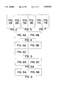
- FIG. 1 is a diagram illustrating two consecutive synchronous transport signal (STS) frames associated with a SONET protocol system, showing how the synchronous payload envelope (SPE) containing the desired digital signal (such as a DS-3 digital signal) can span across such frames.
- STS synchronous transport signal
- SPE synchronous payload envelope
- FIG. 2 is an overall block diagram of the desynchronizer according to the present invention, including circuitry which is fabricated within an ASIC.
- FIG. 3 is a functional block diagram of the leak filter used in the desynchronizer shown in FIG. 1.
- FIG. 4 is a detailed functional block diagram of the leak filter shown in FIG. 3.
- FIG. 5, is a schematic diagram of the sequencer and control circuitry of the calculation engine used to perform the linear branch filtering, integrator branch filtering and fault recovery portions of the desynchronizer.
- FIG. 6 is a schematic diagram of the iterative calculating portion of the calculation engine.
- FIG. 6A is a diagram of the iterative steps and overall calculations performed by the calculation engine.
- FIG. 7 comprising FIGS. 7A and 7B illustrates the partial product results of the calculation engine.
- FIG. 8A is a diagram that illustrates the values of the desynchronizer registers for two set conditions.
- FIG. 8B illustrates the dither, HALFDAC, and integrator output gain values.
- FIG. 9 comprising FIGS. 9A and 9B, illustrates the register contents per shift factor for fast lock and normal states.
- FIG. 10 is a flow diagram of the fault recovery procedure.
- FIG. 11 illustrates waveforms associated with the threshold signal generation, in particular showing the relationship between time and phase response versus various thresholds.
- FIG. 12 is a diagram illustrating the effective phase detector transfer function associated with the desynchronizer.
- the task is therefore to extract the data bytes from the non-dam synchronous overhead bytes and store this incoming periodically discontinuous data stream in a buffer (elastic store) and to extract this data at a rate as close .as possible to its original rate (payload clock or read clock), while accommodating for shifts in the instantaneous incoming data rate as a result of such pointer adjustment and asynchronous stuff bits associated with the payload data itself.
- This latter requirement is complicated by the need to maintain minimal variation in the payload clock rate, since changes in this clock rate are undesirable. It is of course further necessary that such smooth adjustments in the read clock rate occur at a rate that prevents overflow or underflow of the input buffer (elastic store).
- the present invention as best seen in FIG. 2, achieves this desired result by a desynchronizer 20 which comprises an elastic store 22, a nine row averager 24, a leak filter 26, a limiter 28, a pulse width modulation circuit acting as a digital to analog converter 30 and a parallel to serial divide by 8 module 32, all of which can be preferably fabricated as an application specific integrated circuit (ASIC).
- the overall desynchronizer also incorporates an AC to DC converter 34 and a voltage controlled crystal oscillator (VCXO) 36, the latter two modules typically fabricated on a printed circuit assembly associated with the ASIC fabricated modules.
- the specific design shown in FIG. 2 is specifically directed to a desynchronizer for desynchronizing a DS-3 or DS-1 signal from a received SONET signal. The design however is applicable to any synchronous network which uses a payload envelope for containing a digital signal.
- incoming serial data is received on line 40 at input 41 with clock information received on line 42 at input 31 and gapping information on line 44. Gapping information is provided so that only data bytes associated with the digital signal are stored within the elastic store.
- the data is stored in the elastic store as 64 words each 8 bits in length.
- a read clock signal on line 46 is presented to read clock input 33 and the write and read addresses are respectively output on lines 35 and 37.
- the essence of the desynchronizer operation is of course, to read data from the elastic store based upon a read clock signal on line 46 so as to transfer the parallel data to a parallel/serial converter 32 as received on bus 48.
- the output of the parallel/serial converter is a serial bit stream on output 50 (such as a DS-3 signal) which is then used by any interconnected device.
- the data is a DS3 signal extracted from an incoming SONET signal on line 40.
- the desynchronizing of the DS3 signal must account for the variations in the rate of the received data.
- the elastic store thus provides the physical medium for storing incoming data so that the proper data can be extracted therefrom as smoothly as possible.
- the desynchronizer operates as a phase-locked loop (PLL) which comprises four primary components, a phase detector comprising elastic store 22 and 9-row averager 24, the leak filter 26, the VCXO 36, and the parallel/serial divider 32.
- PLL phase-locked loop
- the phase detector 23 comprises elastic store 22 and 9-row averager 24.
- the output of the 9-row averager is the scaled phase difference between the write and read clocks determined from the elastic store write and read addresses.
- the 9-row averager output 52 thus represents the difference between the rate data is being written into the elastic store and the rate it is being read from the elastic store. It is referred to herein as the W-R value.
- the gain from the 9-row averager is a function of the number of 26 MHz clock periods in an 8 KHz frame time (125 microseconds).
- the output 52 of the 9-row averager is a normalized write address minus read address multiplied by the number 26 MHz clock cycles in the 8 KHz frame time. This results in a gain of 3240 counts per byte or 405 counts per bit which can also be represented as 405/(2*PI) counts/radian.
- Leak filter 26 is the device which causes modification of the read clock rate associated with elastic store 32 (DS3 byte clock 46).
- the bandwidth of the leak filter is determined by the coefficients used within leak filter branches 54 and 56. Table 2 sets forth the bandwidth of the in-line linear branch 54 based upon the operating mode of the leak filter as discussed later.
- the peaking of the leak filter transfer function is controlled by the location of the pole from the integrator module 56.
- the VCXO 36 is a discrete implementation having a gain of 5731 radians/seconds/volt maximum and 4776 radians/seconds/volt minimum.
- any modifications to the gain of any of the components within the desynchronizer must be compensated by a change in the coefficients in the bit leaking circuitry so as to maintain the proper bandwidths for minimal jitter.
- the desynchronizer bit leaking capability is shown in increasing detail in FIGS. 3 and 4.
- the linear branch 54 of the leak filter has a nominal gain factor 88 and three increasing gain factors 61 (G1), 63 (G2) and 65 (G2A) which are successively added at summer module 270 that comprises summers 70 and 55 and a 2 -9 (FK5) module 228, as corresponding W-R threshold values 86 (THR -- T1), 87 (THR -- T2) and 89 (THR -- T2A) are exceeded.
- Output 58 of summer 70 also includes the integrator branch output 73. This output is a result of integrator module 114 comprising summer 112, storage register 57 and output shifter 75.
- Gate 110 selects one of the integrator shift factors 90, 91, 93, 95 or 97 and corresponding update rate factors 100, 101, 103, 105 and 107 based upon the presence or absence of W-R thresholds 86, 87, 89 and 60.
- Gate 116 selects the appropriate update rate factor which in turn causes a specific update rate from clock signal 117 to be presented to storage register 57.
- the integrator consists of the integrator shift factors 90, 91, 93, 95, 97, the selector 110, the adder 112, and the register 57, as well as the output scaling factor 75.
- the integrator branch thus provides a long-term storage of the payload read clock frequency.
- the filter when combined with the VCXO transfer function yields an overall type 2 PLL design.
- integrator shift factor module 49 shown in FIG. 3 is a composite of the integrator shift factors and update rate factors.
- the 23-bit sum which is generated by the leak filter (26) is forced to an output equal to 3240 if the sum is greater than 3240 and to 0 if the sum is negative. All sums between 0 and 3240 are passed by the limiter (28) unchanged.
- the D/A converter 30 is actually a decrement counter which functions as a digital to analog converter so as to generate an analog representation of the elastic store fill position.
- the output value of the limiter 28 is loaded into the counter at the beginning of each frame period. Once the counter has loaded the output signal, HALFUL* goes low and remains low until the counter reaches a terminating count of 0.
- the counter decrements at a 26 MHz clock rate. If for example the value loaded into the desynchronizer was 1621, the value of HALFUL* would be low for 1,621 clock cycles and high for 1,619 clock cycles, indicating that the elastic store was just over half full. If the value of TXES representing the store position of the elastic store is half full, then the write minus read difference is 32.
- the loop filter is required to generate a true analog signal.
- the analog signal controls the external VCXO 36 which provides the clock rate for the DS3 byte clock 46.
- the byte clock 46 in turn is used to read the data out of the elastic store.
- dither module 69 generates a 5 bit resolution pseudo random number which is input to summer 55. This random number provides for interpolation between the least significant bits of leak filter output 58 which results in increased resolution of the desynchronizer when operating near the center of the elastic store (W-R ⁇ O).
- the HALFDAC module 53 is input to summer 55 to provide a value to the system when the integrator branch is initialized.
- the HALFDAC value represents the nominal frequency of read clock 46 (see FIG. 2) based upon the specification of the digital signal being extracted (e.g. a 44,736 mb/sec+20 ppm for a DS-3 signal).
- the desynchronizer thus performs the primary functions as set forth in Table 3.
- FIG. 12 also shows the addition of the normal transfer line 59 with the G1 transfer line 372, the G2 transfer line 74 and the G2A transfer line 76, resulting in higher gain for the linear branch as increasing thresholds are detected as defined by the magnitude of the W-R value on output 52.
- a combination of these transfers for the G1 plus G2 thresholds is shown by composite transfer line segment 78, whereas line segment 77 shows the combination of the normal plus G1 gains and line segment 79 shows the transfer function of the normal plus G1 plus G2 plus G2A gains.
- the present invention by use of a calculation engine 82' and 82" as shown in FIGS. 5 and 6 is able to perform the functions of the block diagram shown in FIG. 4 with a limited number of hardware modules.
- the iterative operation of the calculation engine is described in FIG. 6A for each of the event sequences with the column identified as CONDITIONS indicating when that event sequence is performed and the column identified as OTHER FUNCTIONS setting forth what other actions are taken for the execution of that particular sequence.
- a single adder 80 is used instead of a plurality of adders as shown in FIG. 4 to obtain the result of FIG. 4.
- the circuit shown in FIG. 6 as implemented by the steps shown in FIG.
- the calculation engine shown in FIG. 6 is configurable to achieve whatever summing operation and other logic operations are desired. Although the disclosed implementation is for a bit leaker, it is readily apparent that this calculation engine can be configured for other arithmetic and logic operations. Furthermore, although eighteen separate events are calculated to determine the leak filter output value at a given instant of time, since this value only needs to be determined once per frame (125 ⁇ sec), there is sufficient time to perform the iterative calculations when operating at a sufficiently high clock rate, such as 6 MHz.
- the first event sequence takes the output 52 of the 9-row averager as passed through a 2 9 block 25 (which is part of the 9-row averager module 24 shown in FIG. 2) and subtracts the value identified by the ESS module 85 (elastic store center shift value).
- the partial output is identified as POS and represents elastic store position relative to the center, and is performed under all conditions.
- the ESS module provides the ability to have an effectively variable size elastic store, by changing the value of the ESS parameter (85-FIG. 4). This changes the average offset between the read and write clocks in the store, effectively giving a programmable variable sized store (or data delay).
- the average delay would go to 16 bytes--the effective average delay of a 32 byte elastic store.
- this parameter is changeable with a system software update, as are all other significant parameters.
- the leak filter shown in FIGS. 3 and 4 is thus implemented in a recursive fashion so as to avoid separate loops for each adder shown.
- partial products of the linear and integrator branches are iteratively determined in a loop-like fashion.
- the synchronizing of the data path flow through the loop is accomplished by a sequencer 92 and associated control logic shown in FIG. 5.
- FIGS. 8A and 8B set forth two sets of values which can be selected in a preferred embodiment of the present invention.
- FIG. 6 shows that gates 118, 120, 122, and 124, upon receipt of appropriate control signals select the particular shift factors and other inputs required at each sequence event shown in FIG. 6A.
- the ALU control encoder 126 controls adder 80 by output 90 while the register control encoder 128 generates control signals on outputs 129 that control registers 132.
- the multiplexer control encoder 130 via control signals on outputs 131 control gates 118, 120, 122, and 124 while register 133 under input control, controls generation of the desired output on line 72.
- each gain factor requires two consecutive passes through the loop.
- the control logic shown in FIG. 5 dictates which of the gain factors are added during a given frame.
- the event sequence and partial products of the loop are shown in FIGS. 6A and 7 respectively. The sequence is followed on every frame boundary.
- the contents of the loop register after each shift factor is shown in FIG. 9.
- the control logic detects threshold crossings (that is W-R values exceeding predetermined thresholds 86, 87, 89, and 60 shown in FIG. 4) during specific time sequences in a given frame and adds the respective gain factors to the loop.
- the loop monitors these threshold values, namely; gain 1, gain 2, and gain 2a associated with the corresponding linear branch and integrator branch shift factors.
- FIGS. 10, 11 and 12 illustrate the behavior of the fault recovery circuit.
- the gain of the bit leaking filter is adjusted so as to minimize the jitter associated with the generated DS3 byte clock signal 46 and as a result, the read data from the elastic store on output 50.
- jitter on the order of 0.1 to 0.2 unit intervals during pointer events (where one byte equals 8 UI) is easily achievable, or even lower if desired.
- a desynchronizer for obtaining the read clock associated with a payload data signal, such as a DS3 signal embedded within the synchronous payload envelope of a SONET synchronous frame, so as to accommodate pointer movements and asynchronous stuff bit changes in a manner so as to minimize instantaneous change of the read clock rate and thereby instantaneous change of the output frequency associated with the data signal.
- the overall bit leaking circuitry is implemented using a calculation engine which minimizes the number of gates needed to perform the required arithmetic and logic functions through use of an iterative addition/subtraction process wherein partial results are stored in registers and combined in a manner so that the overall result is the same as if the circuitry were implemented in a non-time sequential fashion.
Landscapes
- Engineering & Computer Science (AREA)
- Computer Networks & Wireless Communication (AREA)
- Signal Processing (AREA)
- Synchronisation In Digital Transmission Systems (AREA)
- Time-Division Multiplex Systems (AREA)
- Water Treatment By Electricity Or Magnetism (AREA)
- Treating Waste Gases (AREA)
- Filtering Of Dispersed Particles In Gases (AREA)
Priority Applications (8)
| Application Number | Priority Date | Filing Date | Title |
|---|---|---|---|
| US07/935,008 US5402452A (en) | 1992-08-25 | 1992-08-25 | Incremental phase smoothing desynchronizer and calculation apparatus |
| ES93112765T ES2145755T3 (es) | 1992-08-25 | 1993-08-10 | Desincronizador incremental de alisado de fase y aparato de calculo. |
| AT93112765T ATE192616T1 (de) | 1992-08-25 | 1993-08-10 | Inkrementaler phasenglättungsdesynchronisierer und rechenanordnung |
| EP93112765A EP0584627B1 (de) | 1992-08-25 | 1993-08-10 | Inkrementaler Phasenglättungsdesynchronisierer und Rechenanordnung |
| DE69328521T DE69328521T2 (de) | 1992-08-25 | 1993-08-10 | Inkrementaler Phasenglättungsdesynchronisierer und Rechenanordnung |
| AU44635/93A AU667935B2 (en) | 1992-08-25 | 1993-08-13 | Incremental desynchronizer |
| US08/371,884 US5528530A (en) | 1992-08-25 | 1995-01-12 | Calculation apparatus for performing algebraic and logic computations using iterative calculations and storage of intermediate results |
| AU44441/96A AU692347B2 (en) | 1992-08-25 | 1996-02-09 | Incremental desynchronizer |
Applications Claiming Priority (1)
| Application Number | Priority Date | Filing Date | Title |
|---|---|---|---|
| US07/935,008 US5402452A (en) | 1992-08-25 | 1992-08-25 | Incremental phase smoothing desynchronizer and calculation apparatus |
Related Child Applications (1)
| Application Number | Title | Priority Date | Filing Date |
|---|---|---|---|
| US08/371,884 Division US5528530A (en) | 1992-08-25 | 1995-01-12 | Calculation apparatus for performing algebraic and logic computations using iterative calculations and storage of intermediate results |
Publications (1)
| Publication Number | Publication Date |
|---|---|
| US5402452A true US5402452A (en) | 1995-03-28 |
Family
ID=25466437
Family Applications (2)
| Application Number | Title | Priority Date | Filing Date |
|---|---|---|---|
| US07/935,008 Expired - Lifetime US5402452A (en) | 1992-08-25 | 1992-08-25 | Incremental phase smoothing desynchronizer and calculation apparatus |
| US08/371,884 Expired - Lifetime US5528530A (en) | 1992-08-25 | 1995-01-12 | Calculation apparatus for performing algebraic and logic computations using iterative calculations and storage of intermediate results |
Family Applications After (1)
| Application Number | Title | Priority Date | Filing Date |
|---|---|---|---|
| US08/371,884 Expired - Lifetime US5528530A (en) | 1992-08-25 | 1995-01-12 | Calculation apparatus for performing algebraic and logic computations using iterative calculations and storage of intermediate results |
Country Status (6)
| Country | Link |
|---|---|
| US (2) | US5402452A (de) |
| EP (1) | EP0584627B1 (de) |
| AT (1) | ATE192616T1 (de) |
| AU (2) | AU667935B2 (de) |
| DE (1) | DE69328521T2 (de) |
| ES (1) | ES2145755T3 (de) |
Cited By (24)
| Publication number | Priority date | Publication date | Assignee | Title |
|---|---|---|---|---|
| US5548534A (en) * | 1994-07-08 | 1996-08-20 | Transwitch Corporation | Two stage clock dejitter circuit for regenerating an E4 telecommunications signal from the data component of an STS-3C signal |
| US5598445A (en) * | 1994-03-28 | 1997-01-28 | Alcatel N.V. | Jitter reduction system in digital demultiplexers |
| US5630112A (en) * | 1991-06-19 | 1997-05-13 | Kabushiki Kaisha Toshiba | System using timing information contained in data read from reproduction unit controlled by first oscillator to vary frequency of independent system clock signal |
| US5737373A (en) * | 1994-01-11 | 1998-04-07 | Fujitsu Limited | Control method and apparatus for suppressing jitter |
| US5777998A (en) * | 1993-12-22 | 1998-07-07 | Alcatel N.V. | Method and circuit arrangement for the realization of the higher path adaptation/mapping function in synchronous digital hierarchy/optical network equipment |
| US5781596A (en) * | 1993-11-10 | 1998-07-14 | Northern Telecom Limited | Desynchronising video information from synchronous network to a plesiochronous tributary with constant rate of change in the leak rate |
| US5793824A (en) * | 1996-04-30 | 1998-08-11 | Adtran, Inc. | Digital phase locked loop having adaptive bandwidth for pulse stuffing synchronized digital communication system |
| US5898744A (en) * | 1996-10-07 | 1999-04-27 | Motorola, Inc. | Apparatus and method for clock recovery in a communication system |
| US5956347A (en) * | 1996-04-16 | 1999-09-21 | Marconi Communications Limited | Digital telecommunications transmission systems |
| US6064706A (en) * | 1996-05-01 | 2000-05-16 | Alcatel Usa, Inc. | Apparatus and method of desynchronizing synchronously mapped asynchronous data |
| US6088413A (en) * | 1997-05-09 | 2000-07-11 | Alcatel | Apparatus for reducing jitter in a desynchronizer |
| US6111878A (en) * | 1997-11-04 | 2000-08-29 | Alcatel | Low jitter timing recovery technique and device for asynchronous transfer mode (ATM) constant bit rate (CBR) payloads |
| US6133958A (en) * | 1995-07-29 | 2000-10-17 | Nortel Networks Limited | Broadcast video desynchronizer |
| US20020021719A1 (en) * | 2000-04-28 | 2002-02-21 | Pmc-Sierra, Inc. | Multi-channel SONET/SDH desynchronizer |
| US20020172310A1 (en) * | 2001-05-18 | 2002-11-21 | Manop Thamsirianunt | Jitter attenuator fifo overflow-underflow protection using digital-phase locked loop's bandwidth adaptation |
| US20020186719A1 (en) * | 2001-06-07 | 2002-12-12 | Ravi Subrahmanyan | Pointer adjustment wander and jitter reduction apparatus for a desynchronizer |
| US20040100332A1 (en) * | 2002-11-27 | 2004-05-27 | Broadcom Corporation | System and method for automatic parameter adjustment within a phase locked loop system |
| US20040151134A1 (en) * | 2000-11-23 | 2004-08-05 | Christer Bohm | Switching apparatus |
| US6819725B1 (en) * | 2000-08-21 | 2004-11-16 | Pmc-Sierra, Inc. | Jitter frequency shifting Δ-Σ modulated signal synchronization mapper |
| US20060224659A1 (en) * | 2002-11-06 | 2006-10-05 | Shaohua Yu | Multiple service ring of n-ringlet structure based on multiple fe, ge and 10ge |
| US20070136013A1 (en) * | 2005-12-09 | 2007-06-14 | William Premerlani | Methods and systems for measuring a rate of change of requency |
| US7248588B2 (en) | 1997-09-12 | 2007-07-24 | Alcatel | Method for transmitting data packets and network element for carrying out the method |
| US20070183551A1 (en) * | 2005-04-15 | 2007-08-09 | Huawei Technologies, Co., Ltd. | Method and circuit for obtaining asynchronous demapping clock |
| US8862797B2 (en) | 2011-10-18 | 2014-10-14 | Cortina Systems, Inc. | Reducing delay and delay variation in a buffer in network communications |
Families Citing this family (10)
| Publication number | Priority date | Publication date | Assignee | Title |
|---|---|---|---|---|
| DE69429574T2 (de) * | 1993-11-10 | 2002-09-26 | Nortel Networks Ltd., St.Laurent | Regelung des Ablaufs von Zeigeranpassungsereignissen |
| EP0727887B1 (de) * | 1995-02-16 | 2002-08-28 | Alcatel | Stopfeinrichtung für synchrones digitales Übertragungssystem |
| US5781597A (en) * | 1995-02-16 | 1998-07-14 | Alcatel Sel Aktiengesellschaft | Synchronous digital transmission system having justification circuit that counts frame bytes, calculates offsets, compares thresholds, and initiates justification action |
| DE19820572A1 (de) * | 1998-05-08 | 1999-11-11 | Alcatel Sa | Desynchronisiereinrichtung für ein synchrones digitales Nachrichtenübertragungssystem |
| IT1307715B1 (it) * | 1999-09-30 | 2001-11-14 | Cit Alcatel | Circuito di desincronizzazione di flussi tributari in trame didivisione di tempo in reti di telecomunicazioni e relativo metodo. |
| EP1091289B1 (de) | 1999-10-08 | 2004-05-26 | Hewlett-Packard Company, A Delaware Corporation | Anordnung zur verarbeitung von sonet- oder SDH-DS0-Rahmen zur Kanalzurordnung |
| EP1091288A1 (de) * | 1999-10-08 | 2001-04-11 | Hewlett-Packard Company | Vorrichtung zur Verarbeitung von Sonet- oder SDH-Rahmen mit einem H.100 bus |
| CN1307406A (zh) * | 2000-01-27 | 2001-08-08 | 华为技术有限公司 | 数字锁相环的滤波方法 |
| US6531926B1 (en) * | 2001-09-13 | 2003-03-11 | Overture Networks, Inc. | Dynamic control of phase-locked loop |
| US8019035B2 (en) * | 2003-08-05 | 2011-09-13 | Stmicroelectronics Nv | Noise shaped interpolator and decimator apparatus and method |
Citations (6)
| Publication number | Priority date | Publication date | Assignee | Title |
|---|---|---|---|---|
| US4941156A (en) * | 1987-05-19 | 1990-07-10 | Crystal Semiconductor | Linear jitter attenuator |
| US4996698A (en) * | 1989-10-23 | 1991-02-26 | Rockwell International Corporation | Clock signal resynchronizing apparatus |
| US5052025A (en) * | 1990-08-24 | 1991-09-24 | At&T Bell Laboratories | Synchronous digital signal to asynchronous digital signal desynchronizer |
| US5067126A (en) * | 1989-05-30 | 1991-11-19 | Telecommunications Research Laboratories | Method and apparatus for mapping a digital signal carrier to another |
| US5131013A (en) * | 1990-05-30 | 1992-07-14 | At&T Bell Laboratories | Asynchronous-synchronous digital transmission signal conversion |
| US5200982A (en) * | 1991-10-02 | 1993-04-06 | Alcatel Network Systems, Inc. | In-line piece-wise linear desynchronizer |
Family Cites Families (6)
| Publication number | Priority date | Publication date | Assignee | Title |
|---|---|---|---|---|
| US3564226A (en) * | 1966-12-27 | 1971-02-16 | Digital Equipment | Parallel binary processing system having minimal operational delay |
| US3840861A (en) * | 1972-10-30 | 1974-10-08 | Amdahl Corp | Data processing system having an instruction pipeline for concurrently processing a plurality of instructions |
| US4122534A (en) * | 1977-06-17 | 1978-10-24 | Northern Telecom Limited | Parallel bidirectional shifter |
| JPS6053907B2 (ja) * | 1978-01-27 | 1985-11-27 | 日本電気株式会社 | 二項ベクトル乗算回路 |
| DE3066955D1 (en) * | 1980-06-24 | 1984-04-19 | Ibm | Signal processor computing arrangement and method of operating said arrangement |
| US4901267A (en) * | 1988-03-14 | 1990-02-13 | Weitek Corporation | Floating point circuit with configurable number of multiplier cycles and variable divide cycle ratio |
-
1992
- 1992-08-25 US US07/935,008 patent/US5402452A/en not_active Expired - Lifetime
-
1993
- 1993-08-10 DE DE69328521T patent/DE69328521T2/de not_active Expired - Lifetime
- 1993-08-10 ES ES93112765T patent/ES2145755T3/es not_active Expired - Lifetime
- 1993-08-10 EP EP93112765A patent/EP0584627B1/de not_active Expired - Lifetime
- 1993-08-10 AT AT93112765T patent/ATE192616T1/de not_active IP Right Cessation
- 1993-08-13 AU AU44635/93A patent/AU667935B2/en not_active Ceased
-
1995
- 1995-01-12 US US08/371,884 patent/US5528530A/en not_active Expired - Lifetime
-
1996
- 1996-02-09 AU AU44441/96A patent/AU692347B2/en not_active Ceased
Patent Citations (6)
| Publication number | Priority date | Publication date | Assignee | Title |
|---|---|---|---|---|
| US4941156A (en) * | 1987-05-19 | 1990-07-10 | Crystal Semiconductor | Linear jitter attenuator |
| US5067126A (en) * | 1989-05-30 | 1991-11-19 | Telecommunications Research Laboratories | Method and apparatus for mapping a digital signal carrier to another |
| US4996698A (en) * | 1989-10-23 | 1991-02-26 | Rockwell International Corporation | Clock signal resynchronizing apparatus |
| US5131013A (en) * | 1990-05-30 | 1992-07-14 | At&T Bell Laboratories | Asynchronous-synchronous digital transmission signal conversion |
| US5052025A (en) * | 1990-08-24 | 1991-09-24 | At&T Bell Laboratories | Synchronous digital signal to asynchronous digital signal desynchronizer |
| US5200982A (en) * | 1991-10-02 | 1993-04-06 | Alcatel Network Systems, Inc. | In-line piece-wise linear desynchronizer |
Non-Patent Citations (28)
| Title |
|---|
| "Design and Performance Verification of a SONET-TO-DS3 Desynchronizer", Hamlin, Jr., TranSwitch Corp. Shelton, Connecticut, published before Feb. 25, 1992. |
| 1991 "Jitter reduction in SDH networks"SAT France H. Sari and G. Karam. pp. 1413-1417. |
| 1991 Jitter reduction in SDH networks SAT France H. Sari and G. Karam. pp. 1413 1417. * |
| Design and Performance Verification of a SONET TO DS3 Desynchronizer , Hamlin, Jr., TranSwitch Corp. Shelton, Connecticut, published before Feb. 25, 1992. * |
| T1 LB280 A Technical Report on the Effects of SONET on Payload Oytput Jitter, T1X1.3. * |
| T1 LB280-"A Technical Report on the Effects of SONET on Payload Oytput Jitter," T1X1.3. |
| T1.105 1991 Digital Hierarchy Optical Interface Rates and Formats Specification (SONET), Section 7 Synchronization. * |
| T1.105-1991 "Digital Hierarchy-Optical Interface Rates and Formats Specification" (SONET), Section 7 Synchronization. |
| T1X1.3/92 017 Additional SONET Islands Jitter Simulation Results, Alcatel. * |
| T1X1.3/92 071 Jitter Accumulation Results in SONET Islands for Mill Hertz NE Clock Bandwidths, Alcatel. * |
| T1X1.3/92 072 DS3 Payload Output Jitter Proposal, Alcatel. * |
| T1X1.3/92-017-"Additional SONET Islands Jitter Simulation Results," Alcatel. |
| T1X1.3/92-071-"Jitter Accumulation Results in SONET Islands for Mill-Hertz NE Clock Bandwidths," Alcatel. |
| T1X1.3/92-072-"DS3 Payload Output Jitter Proposal," Alcatel. |
| T1X1.392 006 Initial Draft of SONET Jitter Standard, Tellabs. * |
| T1X1.392-006-"Initial Draft of SONET Jitter Standard," Tellabs. |
| T1X1.6/88 026 A Synchronous Desynchronizer. Bellcore Signals:, Bellcore. * |
| T1X1.6/88 028 Analysis of Jitter & Wander Associated with Pointer Adjustments, British Telecom. * |
| T1X1.6/88 029 A Possible Design for a Desynchronizer Accomodating Pointer Adjustments, British Telecom. * |
| T1X1.6/88 041 Pointer Spreading Desynchronizer, Northern Telecom. * |
| T1X1.6/88-026-"A Synchronous Desynchronizer." Bellcore Signals:, Bellcore. |
| T1X1.6/88-028-"Analysis of Jitter & Wander Associated with Pointer Adjustments," British Telecom. |
| T1X1.6/88-029-"A Possible Design for a Desynchronizer Accomodating Pointer Adjustments," British Telecom. |
| T1X1.6/88-041-"Pointer Spreading Desynchronizer," Northern Telecom. |
| T1X1.6/89 029 Results of Simulations of a Possible Desynchronizer Design, British Telecom. * |
| T1X1.6/89-029-"Results of Simulations of a Possible Desynchronizer Design," British Telecom. |
| T1X1.6/90 005 STS 1 and OC N Jitter Proposal, Alcatel. * |
| T1X1.6/90-005-"STS-1 and OC-N Jitter Proposal," Alcatel. |
Cited By (31)
| Publication number | Priority date | Publication date | Assignee | Title |
|---|---|---|---|---|
| US5630112A (en) * | 1991-06-19 | 1997-05-13 | Kabushiki Kaisha Toshiba | System using timing information contained in data read from reproduction unit controlled by first oscillator to vary frequency of independent system clock signal |
| US5781596A (en) * | 1993-11-10 | 1998-07-14 | Northern Telecom Limited | Desynchronising video information from synchronous network to a plesiochronous tributary with constant rate of change in the leak rate |
| US5777998A (en) * | 1993-12-22 | 1998-07-07 | Alcatel N.V. | Method and circuit arrangement for the realization of the higher path adaptation/mapping function in synchronous digital hierarchy/optical network equipment |
| US5737373A (en) * | 1994-01-11 | 1998-04-07 | Fujitsu Limited | Control method and apparatus for suppressing jitter |
| US5598445A (en) * | 1994-03-28 | 1997-01-28 | Alcatel N.V. | Jitter reduction system in digital demultiplexers |
| US5548534A (en) * | 1994-07-08 | 1996-08-20 | Transwitch Corporation | Two stage clock dejitter circuit for regenerating an E4 telecommunications signal from the data component of an STS-3C signal |
| US6133958A (en) * | 1995-07-29 | 2000-10-17 | Nortel Networks Limited | Broadcast video desynchronizer |
| US5956347A (en) * | 1996-04-16 | 1999-09-21 | Marconi Communications Limited | Digital telecommunications transmission systems |
| US5793824A (en) * | 1996-04-30 | 1998-08-11 | Adtran, Inc. | Digital phase locked loop having adaptive bandwidth for pulse stuffing synchronized digital communication system |
| US6064706A (en) * | 1996-05-01 | 2000-05-16 | Alcatel Usa, Inc. | Apparatus and method of desynchronizing synchronously mapped asynchronous data |
| US5898744A (en) * | 1996-10-07 | 1999-04-27 | Motorola, Inc. | Apparatus and method for clock recovery in a communication system |
| US6088413A (en) * | 1997-05-09 | 2000-07-11 | Alcatel | Apparatus for reducing jitter in a desynchronizer |
| US7248588B2 (en) | 1997-09-12 | 2007-07-24 | Alcatel | Method for transmitting data packets and network element for carrying out the method |
| US6111878A (en) * | 1997-11-04 | 2000-08-29 | Alcatel | Low jitter timing recovery technique and device for asynchronous transfer mode (ATM) constant bit rate (CBR) payloads |
| US6982995B2 (en) | 2000-04-28 | 2006-01-03 | Pmc-Sierra, Inc. | Multi-channel SONET/SDH desynchronizer |
| US20020021719A1 (en) * | 2000-04-28 | 2002-02-21 | Pmc-Sierra, Inc. | Multi-channel SONET/SDH desynchronizer |
| US6819725B1 (en) * | 2000-08-21 | 2004-11-16 | Pmc-Sierra, Inc. | Jitter frequency shifting Δ-Σ modulated signal synchronization mapper |
| US7356025B2 (en) * | 2000-11-23 | 2008-04-08 | Net Insight Ab | Switching apparatus for switching data between bitstreams |
| US20040151134A1 (en) * | 2000-11-23 | 2004-08-05 | Christer Bohm | Switching apparatus |
| US20020172310A1 (en) * | 2001-05-18 | 2002-11-21 | Manop Thamsirianunt | Jitter attenuator fifo overflow-underflow protection using digital-phase locked loop's bandwidth adaptation |
| US20020186719A1 (en) * | 2001-06-07 | 2002-12-12 | Ravi Subrahmanyan | Pointer adjustment wander and jitter reduction apparatus for a desynchronizer |
| US6882662B2 (en) | 2001-06-07 | 2005-04-19 | Applied Micro Circuits Corporation | Pointer adjustment wander and jitter reduction apparatus for a desynchronizer |
| US20060224659A1 (en) * | 2002-11-06 | 2006-10-05 | Shaohua Yu | Multiple service ring of n-ringlet structure based on multiple fe, ge and 10ge |
| US7778162B2 (en) | 2002-11-06 | 2010-08-17 | Wuhan Fiberhome Networks Co. Ltd. | Multiple service ring of N-ringlet structure based on multiple FE, GE and 10GE |
| US20040100332A1 (en) * | 2002-11-27 | 2004-05-27 | Broadcom Corporation | System and method for automatic parameter adjustment within a phase locked loop system |
| US6762649B2 (en) * | 2002-11-27 | 2004-07-13 | Broadcom Corporation | System and method for automatic parameter adjustment within a phase locked loop system |
| US20070183551A1 (en) * | 2005-04-15 | 2007-08-09 | Huawei Technologies, Co., Ltd. | Method and circuit for obtaining asynchronous demapping clock |
| US8090066B2 (en) * | 2005-04-15 | 2012-01-03 | Huawei Technologies Co., Ltd. | Method and circuit for obtaining asynchronous demapping clock |
| US20070136013A1 (en) * | 2005-12-09 | 2007-06-14 | William Premerlani | Methods and systems for measuring a rate of change of requency |
| US7328114B2 (en) | 2005-12-09 | 2008-02-05 | General Electric Company | Methods and systems for measuring a rate of change of frequency |
| US8862797B2 (en) | 2011-10-18 | 2014-10-14 | Cortina Systems, Inc. | Reducing delay and delay variation in a buffer in network communications |
Also Published As
| Publication number | Publication date |
|---|---|
| AU4444196A (en) | 1996-06-13 |
| EP0584627B1 (de) | 2000-05-03 |
| ES2145755T3 (es) | 2000-07-16 |
| US5528530A (en) | 1996-06-18 |
| AU4463593A (en) | 1994-03-03 |
| AU692347B2 (en) | 1998-06-04 |
| ATE192616T1 (de) | 2000-05-15 |
| DE69328521T2 (de) | 2001-03-15 |
| EP0584627A3 (en) | 1996-05-29 |
| EP0584627A2 (de) | 1994-03-02 |
| DE69328521D1 (de) | 2000-06-08 |
| AU667935B2 (en) | 1996-04-18 |
Similar Documents
| Publication | Publication Date | Title |
|---|---|---|
| US5402452A (en) | Incremental phase smoothing desynchronizer and calculation apparatus | |
| US5404380A (en) | Desynchronizer for adjusting the read data rate of payload data received over a digital communication network transmitting payload data within frames | |
| US5268936A (en) | Synchronous digital signal to asynchronous digital signal desynchronizer | |
| EP0549125B1 (de) | Desynchronisierer von synchronen digitalen Signalen zu asynchronen digitalen Signalen | |
| US5390180A (en) | SONET DS-N desynchronizer | |
| US5457717A (en) | Apparatus and method for eliminating mapping jitter | |
| EP0626117B1 (de) | Desynchronisierer und verfahren zur unterdrückung des zeigerzitterns in einen desynchronisierer | |
| US6744787B1 (en) | Adaptive phase shift filtration of pointer justification jitter in synchronous-plesiosynchronous signal desynchronization | |
| EP0473338B1 (de) | Bitsynchronisierung mittels elastisches Speichers | |
| US5311511A (en) | SONET DS-N desynchronizer | |
| EP0535698B1 (de) | Linearer In-line-Desynchronisierer | |
| US5699391A (en) | Digital desynchronizer | |
| JPH1117638A (ja) | デシンクロナイザ中のジッタを低減させる装置 | |
| EP1400079B1 (de) | Verfahren und vorrichtung zum entsynchronisieren eines ds-3-signals und/oder eines e3-signals aus dem datenteil eines sts/stm-nutzsignals | |
| US5793824A (en) | Digital phase locked loop having adaptive bandwidth for pulse stuffing synchronized digital communication system | |
| US5539785A (en) | Jitter/wander reduction circuit for pulse-stuffed, synchronized digital communications | |
| CA2063930C (en) | Synchronous digital signal to asynchronous digital signal desynchronizer | |
| EP0492549B1 (de) | Verfahren zur Reduzierung von Phasenrauschen verursacht in einem SDH-Netzwerk mittels Zeichenstopftechnik, und integrierte Schaltungen geeignet zur Implementierung dieses Verfahrens | |
| US7440533B2 (en) | Modulated jitter attenuation filter | |
| JP2963194B2 (ja) | ジッタ抑圧回路 | |
| KR20010003166A (ko) | 디지털 위상동기루프를 이용한 브이씨12 디맵퍼 | |
| JPH0927747A (ja) | ディジタルpll回路 |
Legal Events
| Date | Code | Title | Description |
|---|---|---|---|
| AS | Assignment |
Owner name: ALCATEL NETWORK SYSTEMS, INC., TEXAS Free format text: ASSIGNMENT OF ASSIGNORS INTEREST.;ASSIGNORS:POWELL, WILLIAM E.;WEEBER, WILLIAM B.;AFIFY, MANAL E.;REEL/FRAME:006285/0170 Effective date: 19921012 |
|
| STCF | Information on status: patent grant |
Free format text: PATENTED CASE |
|
| FEPP | Fee payment procedure |
Free format text: PAYOR NUMBER ASSIGNED (ORIGINAL EVENT CODE: ASPN); ENTITY STATUS OF PATENT OWNER: LARGE ENTITY |
|
| FPAY | Fee payment |
Year of fee payment: 4 |
|
| FPAY | Fee payment |
Year of fee payment: 8 |
|
| FPAY | Fee payment |
Year of fee payment: 12 |