US5355213A - Inspection system for detecting surface flaws - Google Patents
Inspection system for detecting surface flaws Download PDFInfo
- Publication number
- US5355213A US5355213A US07/976,862 US97686292A US5355213A US 5355213 A US5355213 A US 5355213A US 97686292 A US97686292 A US 97686292A US 5355213 A US5355213 A US 5355213A
- Authority
- US
- United States
- Prior art keywords
- transparent element
- radiation
- transparent
- angle
- inspected
- Prior art date
- Legal status (The legal status is an assumption and is not a legal conclusion. Google has not performed a legal analysis and makes no representation as to the accuracy of the status listed.)
- Expired - Fee Related
Links
- 238000007689 inspection Methods 0.000 title claims abstract description 29
- 230000005855 radiation Effects 0.000 claims abstract description 56
- 230000005670 electromagnetic radiation Effects 0.000 claims abstract description 13
- 238000000034 method Methods 0.000 claims description 30
- 239000000356 contaminant Substances 0.000 claims description 16
- 230000007547 defect Effects 0.000 claims description 11
- 230000003287 optical effect Effects 0.000 claims description 4
- 230000000149 penetrating effect Effects 0.000 claims description 4
- 229910052736 halogen Inorganic materials 0.000 claims description 3
- 150000002367 halogens Chemical class 0.000 claims description 3
- 229910052724 xenon Inorganic materials 0.000 claims description 3
- FHNFHKCVQCLJFQ-UHFFFAOYSA-N xenon atom Chemical compound [Xe] FHNFHKCVQCLJFQ-UHFFFAOYSA-N 0.000 claims description 3
- 239000011159 matrix material Substances 0.000 abstract description 4
- 238000000576 coating method Methods 0.000 description 3
- 238000011109 contamination Methods 0.000 description 3
- 239000011248 coating agent Substances 0.000 description 2
- 238000001514 detection method Methods 0.000 description 2
- 239000011521 glass Substances 0.000 description 2
- 239000000463 material Substances 0.000 description 2
- 230000005856 abnormality Effects 0.000 description 1
- 230000009365 direct transmission Effects 0.000 description 1
- 239000000835 fiber Substances 0.000 description 1
- 238000003384 imaging method Methods 0.000 description 1
- 230000003993 interaction Effects 0.000 description 1
- 238000005305 interferometry Methods 0.000 description 1
- 239000004973 liquid crystal related substance Substances 0.000 description 1
- 238000012986 modification Methods 0.000 description 1
- 230000004048 modification Effects 0.000 description 1
- 230000035945 sensitivity Effects 0.000 description 1
- 239000012780 transparent material Substances 0.000 description 1
- 238000011179 visual inspection Methods 0.000 description 1
Images


Classifications
-
- G—PHYSICS
- G01—MEASURING; TESTING
- G01N—INVESTIGATING OR ANALYSING MATERIALS BY DETERMINING THEIR CHEMICAL OR PHYSICAL PROPERTIES
- G01N21/00—Investigating or analysing materials by the use of optical means, i.e. using sub-millimetre waves, infrared, visible or ultraviolet light
- G01N21/84—Systems specially adapted for particular applications
- G01N21/88—Investigating the presence of flaws or contamination
- G01N21/95—Investigating the presence of flaws or contamination characterised by the material or shape of the object to be examined
- G01N21/958—Inspecting transparent materials or objects, e.g. windscreens
-
- G—PHYSICS
- G01—MEASURING; TESTING
- G01N—INVESTIGATING OR ANALYSING MATERIALS BY DETERMINING THEIR CHEMICAL OR PHYSICAL PROPERTIES
- G01N21/00—Investigating or analysing materials by the use of optical means, i.e. using sub-millimetre waves, infrared, visible or ultraviolet light
- G01N21/84—Systems specially adapted for particular applications
- G01N21/88—Investigating the presence of flaws or contamination
- G01N21/8806—Specially adapted optical and illumination features
-
- G—PHYSICS
- G01—MEASURING; TESTING
- G01N—INVESTIGATING OR ANALYSING MATERIALS BY DETERMINING THEIR CHEMICAL OR PHYSICAL PROPERTIES
- G01N21/00—Investigating or analysing materials by the use of optical means, i.e. using sub-millimetre waves, infrared, visible or ultraviolet light
- G01N21/84—Systems specially adapted for particular applications
- G01N21/88—Investigating the presence of flaws or contamination
- G01N21/89—Investigating the presence of flaws or contamination in moving material, e.g. running paper or textiles
- G01N21/892—Investigating the presence of flaws or contamination in moving material, e.g. running paper or textiles characterised by the flaw, defect or object feature examined
- G01N21/896—Optical defects in or on transparent materials, e.g. distortion, surface flaws in conveyed flat sheet or rod
Definitions
- the present invention relates to an apparatus and a method for detecting surface flaws or contaminants of transparent members, and more particularly, to an apparatus and an automated method using the apparatus for inspecting and detecting, using electromagnetic radiation, the presence of surface flaws and contaminants in the planar or curved surfaces of members which are transparent to the electromagnetic radiation.
- the present invention can also be applied in the inspection of low contrast marks engraved or coated on transparent elements.
- Surface flaws can be of a variety of types.
- the word ⁇ flaw ⁇ as used herein is meant to include all types of surface defects such as scratches, digs, pits, chips, and other abnormalities and irregularities which tend to create surface discontinuities. Included also are contaminants which adhere to, or are in contact with, the outer surface of the transparent member, including also contaminants and defects in transparent coatings on the surface.
- the inspection process has been automated to some extent.
- instruments which can aid in the inspection for surface flaws.
- systems which illuminate the member inspected with a flying spot and which detect the scattered light in the black zone.
- interferometry principles by detecting interference-patterns created by the interaction of light which passes through the inspected element and a reference light beam.
- an inspection system for detecting surface features, such as flaws, contaminants, or surface marks, in a transparent element, comprising: a source of electromagnetic radiation; directing means for directing the radiation edgewise into the transparent element at such an angle that the angle between the radiation penetrating the element and the surface of the element is larger than the critical angle so that substantially all of the radiation will stay within the transparent element and exit through an opposing edge of the transparent element unless a surface flaw is encountered, in which case a portion of the radiation will exit the transparent element through the surface of the transparent element; a detector capable of detecting the portion of the radiation which exits the transparent element through the surface of the transparent element and of producing signals corresponding to the exiting radiation; and a signal processor capable of processing the signals corresponding to the exiting radiation.
- a method of inspecting surface features, such as flaws, contaminants or surface marks, in a transparent element comprising: directing electromagnetic radiation edgewise into the transparent element at an such an angle that the angle between the radiation penetrating the element and the surface of the element is larger than the critical angle so that substantially all of the radiation will stay within the transparent element and exit through an opposing edge of the transparent element unless a surface flaw is encountered, in which case a portion of the radiation will exit the transparent element through the surface of the transparent element; detecting the portion of the radiation which exits the transparent element through the surface of the transparent element and producing signals corresponding to the exiting radiation; and processing the signals corresponding to the exiting radiation.
- means for moving the transparent element so as to present different portions of the transparent element for inspection, whether by translation or rotation, or both.
- the transparent element is kept stationary and the electromagnetic radiation, and, in some cases, the detector, are moved to achieve inspection of the entire transparent element.
- a system and method according to the present invention overcomes problems associated with the automatic inspection of defects in transparent elements.
- Transparent elements having flat or smoothly curved surfaces can be accommodated.
- Internal defects include bubbles, cracks and other non-surface irregularities which cause non-homogeneity in the material.
- Detection of flaws is accomplished by directing radiation edgewise into the element and sensing the radiation which emerges through the element surface.
- the radiation introduced edgewise into the element is typically a narrow beam, which is introduced in such a way that the radiation enters the transparent element to form an angle between the penetrating radiation and the surface to be inspected which is greater, preferably only slightly greater, than the critical angle.
- the radiation is preferably directed so that the internal reflecting angle is only slightly larger than the critical angle in order to enhance the sensitivity of the system.
- the internal reflection angle is only slightly above the critical, even small imperfections in the surface will cause a portion of the radiation to escape the element, thereby providing an indication of the presence of a flaw.
- polarized light it is preferred to use polarized light.
- the scanning can be accomplished in a number of ways, such as by linearly translating or rotating the inspected element.
- the emerging light is imaged on a line scan camera, which is aligned parallel to the light beam, or on any other suitable detector.
- Inspected elements of sufficiently small size may be inspected in their entirety with a single radiation beam without the need to scan the element.
- the emerged light may be imaged on a matrix camera (like CCD) or on any other suitable detector.
- the signal of the multi-element line detector, or scan camera, or matrix or array camera, or other detector is processed, for example using a frame grabber and image processor, in order to convert the signals produced by the detector to information useful in identifying the presence, and, when desired, the location, of the flaw.
- the processor preferably takes advantage of algorithms to optimize the detection and reduce false alarms. Any suitable signal processor may be used. For example threshold signal processing may be applied to determine the signal caused by the flaw.
- the inspection system and method according to the present invention have several advantages over currently known inspection methods.
- the inspection system and method according to the present invention are capable of detecting flaws and contaminants, on one or on both surfaces of the element, as well as in the interior of the inspected element and in its surface coating.
- the signal to noise ratio at the detector plane is high, since if no defects are present, almost no light emerges from the element through its surface. This is because, in the absence of flaws, the entire light beam is totally internal reflected within the element. Therefore, the noise is basically the detector noise. The only signal which reaches the detector, is caused by the light exiting the element surface following impingement upon the flaws or contaminants.
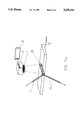
- FIG. I is a schematic depiction of an inspection method and system according to the present invention.
- FIG. 2a shows the system of FIG. 1 where the inspected element can be translated linearly
- FIG. 2b shows the system of FIG. 1 where the inspected element can be rotated about a vertical
- FIG. 2c shows the system of FIG. 1 where the inspected element can be rotated about its axis.
- FIG. 3 shows a system according to the present invention wherein a single beam is able to illuminate the entire inspected surface of the element without the need to move either the beam or the element;
- FIG. 4 shows the method and system as in FIG. 1 but using a lens to act on a single radiation beam so as to effectively form a plurality of "beams".
- the present invention is of an apparatus and a method of inspecting a transparent element for surface flaws.
- the principles and operation of an apparatus and a method according to the present invention may be better understood with reference to the figures and embodiments described below.
- FIG. 1 depicts an inspection method and system for detecting flaws or contamination on a surface 1a of a transparent element 2.
- the element is made of a transparent material, and has surfaces 1a and 1b.
- Surfaces 1a and 1b are depicted as being parallel to each other. While such a configuration is convenient, it is not essential for the operation of a method or a system according to the present invention. Elements with non-parallel surfaces, even with curved surfaces, can also be inspected.
- An electromagnetic radiation source 6 illuminates transparent element 2 at one of its edges 3.
- Any convenient electromagnetic radiation may be used, for example, laser beams.
- any convenient narrow-band light sources such as those based on xenon or halogens.
- Indicated in FIG. 1 are two solid-state lasers. The use of two beams, as depicted in FIG. 1, provides complete coverage of the entire surface to be inspected.
- a single beam may be generated and subsequently split into two beams by optical manipulation.
- a lens 11 preferably a fast lens, or cylindrical lens, which serves to effectively generate two "beams”. It may also be possible to use a single beam and vary its position and/or the position of element 2 to sequentially scan the entire surface to be inspected.
- Radiation sources 6 produce radiation beams 7a which are directed in an angle "A", such that the internal rays 7b, which are the rays after their entry into transparent element 2, strike surfaces 1a and 1b at an angle "B" which is slightly greater than the critical angle.
- Various directing means may be used to direct the radiation from sources 6 to the object. These include, but are not limited to, direct transmission through the air, and the use of optical light guides.
- the latter may include fiber optics and may optionally further include a lens or lenses.
- Line CCD 8 senses the emitted light and transmits a signal to a signal processor 10. If no surface flaws or contaminants are encountered, almost no light leaves through surface 1a, and so no radiation reaches line CCD 8.
- transparent element 2 is moved perpendicularly to the radiation beam 7a, so the whole area of the element is scanned.
- the movement is carried out in such a way as to ensure that radiation beam 7a always enters element 2 through its edge 3.
- element 2 may be held steady while radiation beam 7b, and possibly other portion of the system, are moved.
- both element 2 and radiation beam 7b may be moved in some coordinated fashion to achieve the objective of subjecting the entire surface of element 2 for inspection.
- element 2 can be moved linearly in direction "V" as shown in FIG. 2a. If the element is substantially disk-shaped, it can be rotated about its axis, as shown in FIG. 2b. If the element is substantially a hollow cylinder, radiation beam 7a is directed to the cylinder base, and the cylinder can be rotated about its axis, as shown in FIG. 2c. Alternatively, element 2 can be held in a fixed position and radiation beam 7a and, if necessary, CCD 8 (which may include electronic components, making it a camera), can be moved so as to scan the surface of element 2 for flaws and contaminants.
- CCD 8 which may include electronic components, making it a camera
- the signal produced by line scan camera 8 is processed by an image processor 10 in order to detect and identify the signals from the flaw or contamination, and so to eliminate false alarms.
- CCD 8 a matrix CCD 8 is used, and surface 1a is focused on it by lens 9.
- the signal of CCD 8 (which may include electronic components, making it a camera), is processed by image processor 10 in order to identify the flaw and eliminate false alarms.
Abstract
An inspection system for detecting surface flaws in a transparent element which includes a source of electromagnetic radiation, such as a laser beam or visible light, with the radiation beam directed edgewise into the transparent element to be inspected at such an angle that the resulting internal angle is larger than the critical angle. This ensures that substantially all of the radiation will stay within the transparent element and exit through an opposing edge of the transparent element unless a surface flaw is encountered, in which case a portion of the radiation will exit the transparent element through the surface of the transparent element. The system includes a detector, such as a line or matrix charge coupled device, capable of detecting the portion of the radiation which exits the transparent element through the surface of the transparent element and of producing signals corresponding to the exiting radiation.
Description
The present invention relates to an apparatus and a method for detecting surface flaws or contaminants of transparent members, and more particularly, to an apparatus and an automated method using the apparatus for inspecting and detecting, using electromagnetic radiation, the presence of surface flaws and contaminants in the planar or curved surfaces of members which are transparent to the electromagnetic radiation.
Precision components in a great variety of applications require for their proper operation that their surface be essentially free of flaws and contaminants. A significant fraction of such components are made of materials which are transparent to electromagnetic radiation. Examples are the glass substrata used in Liquid Crystal Displays (LCD's) or other Flat Panel Displays (FPD's), windows for Charge Coupled Devices (CCD's) detectors, contact lenses, miniature lenses, glass substrata for rigid disks, etc. For these and similar components, it is imperative that the critical surfaces be virtually free of surface flaws.
In addition, the present invention can also be applied in the inspection of low contrast marks engraved or coated on transparent elements.
Surface flaws can be of a variety of types. The word `flaw` as used herein is meant to include all types of surface defects such as scratches, digs, pits, chips, and other abnormalities and irregularities which tend to create surface discontinuities. Included also are contaminants which adhere to, or are in contact with, the outer surface of the transparent member, including also contaminants and defects in transparent coatings on the surface.
Since surface flaws are typically very small, it is normally very difficult to detect the defects, specially with high speed automatic systems.
Surface flaw inspection on transparent objects is currently performed largely by visual inspection carried out by human inspectors. The process is labor-intensive and often unreliable.
The inspection process has been automated to some extent. There are currently a number of instruments which can aid in the inspection for surface flaws. For example, systems are known which illuminate the member inspected with a flying spot and which detect the scattered light in the black zone. It is also known to use interferometry principles by detecting interference-patterns created by the interaction of light which passes through the inspected element and a reference light beam.
However these methods suffer from low detectability capabilities, a slow inspection rate which results in low inspection rates, and difficulty in the inspection on non-flat surfaces.
In addition, the existing methods cannot be accurately applied for the inspection of defects in low contrast marks engraved or coated on transparent elements such as in reticles, conductive lines, etc.
There is thus a widely recognized need for an apparatus and a method of inspecting the surface of transparent elements for flaws which can accurately detect the presence of such flaws and which can be used in an automated fashion requiring little or no human judgment.
It would be desirable to have an inspection system for detecting surface flaws which would quickly and reliably determine the presence of surface flaws.
According to the present invention there is provided an inspection system for detecting surface features, such as flaws, contaminants, or surface marks, in a transparent element, comprising: a source of electromagnetic radiation; directing means for directing the radiation edgewise into the transparent element at such an angle that the angle between the radiation penetrating the element and the surface of the element is larger than the critical angle so that substantially all of the radiation will stay within the transparent element and exit through an opposing edge of the transparent element unless a surface flaw is encountered, in which case a portion of the radiation will exit the transparent element through the surface of the transparent element; a detector capable of detecting the portion of the radiation which exits the transparent element through the surface of the transparent element and of producing signals corresponding to the exiting radiation; and a signal processor capable of processing the signals corresponding to the exiting radiation.
According to the present invention there is also provided a method of inspecting surface features, such as flaws, contaminants or surface marks, in a transparent element, comprising: directing electromagnetic radiation edgewise into the transparent element at an such an angle that the angle between the radiation penetrating the element and the surface of the element is larger than the critical angle so that substantially all of the radiation will stay within the transparent element and exit through an opposing edge of the transparent element unless a surface flaw is encountered, in which case a portion of the radiation will exit the transparent element through the surface of the transparent element; detecting the portion of the radiation which exits the transparent element through the surface of the transparent element and producing signals corresponding to the exiting radiation; and processing the signals corresponding to the exiting radiation.
According to further features in preferred embodiments of the invention described below, there is provided means for moving the transparent element. so as to present different portions of the transparent element for inspection, whether by translation or rotation, or both.
According to an alternative embodiment, the transparent element is kept stationary and the electromagnetic radiation, and, in some cases, the detector, are moved to achieve inspection of the entire transparent element.
A system and method according to the present invention overcomes problems associated with the automatic inspection of defects in transparent elements. Transparent elements having flat or smoothly curved surfaces can be accommodated.
Various types of flaws on the element surface, including coating defects and contamination, can be detected, as can, incidentally, a number of internal defects. Internal defects include bubbles, cracks and other non-surface irregularities which cause non-homogeneity in the material.
Detection of flaws is accomplished by directing radiation edgewise into the element and sensing the radiation which emerges through the element surface. The radiation introduced edgewise into the element is typically a narrow beam, which is introduced in such a way that the radiation enters the transparent element to form an angle between the penetrating radiation and the surface to be inspected which is greater, preferably only slightly greater, than the critical angle.
Introducing the radiation at an angle which is greater than the critical angle ensures that, in the absence of flaws, total internal reflection is achieved and the incident light stays within the transparent element until it reaches the far end of the element where the radiation leaves the element through the far edge of the element.
When a surface flaw exists, some of the radiation will not be internally reflected upon impinging upon the flaw, but will rather escape through the surface of the transparent element. The radiation is preferably directed so that the internal reflecting angle is only slightly larger than the critical angle in order to enhance the sensitivity of the system. When the internal reflection angle is only slightly above the critical, even small imperfections in the surface will cause a portion of the radiation to escape the element, thereby providing an indication of the presence of a flaw. Furthermore, to enhance the light emerging from the element it is preferred to use polarized light.
The scanning can be accomplished in a number of ways, such as by linearly translating or rotating the inspected element. The emerging light is imaged on a line scan camera, which is aligned parallel to the light beam, or on any other suitable detector.
Inspected elements of sufficiently small size may be inspected in their entirety with a single radiation beam without the need to scan the element. In such a case the emerged light may be imaged on a matrix camera (like CCD) or on any other suitable detector.
The signal of the multi-element line detector, or scan camera, or matrix or array camera, or other detector, is processed, for example using a frame grabber and image processor, in order to convert the signals produced by the detector to information useful in identifying the presence, and, when desired, the location, of the flaw. The processor preferably takes advantage of algorithms to optimize the detection and reduce false alarms. Any suitable signal processor may be used. For example threshold signal processing may be applied to determine the signal caused by the flaw.
For inspection of marks on an element, the method and system configuration are virtually identical with those described above for flaw inspection, with differences in the signal processing and interpretation of the results.
Systems and methods according to the present invention have several advantages over currently known inspection methods. In contrast with presently known techniques, the inspection system and method according to the present invention are capable of detecting flaws and contaminants, on one or on both surfaces of the element, as well as in the interior of the inspected element and in its surface coating.
The signal to noise ratio at the detector plane is high, since if no defects are present, almost no light emerges from the element through its surface. This is because, in the absence of flaws, the entire light beam is totally internal reflected within the element. Therefore, the noise is basically the detector noise. The only signal which reaches the detector, is caused by the light exiting the element surface following impingement upon the flaws or contaminants.
The use of an imaging system for detecting the flaws makes it possible to eliminate false alarm, and ensure reliable automatic inspection, through the use of image processing.
A more complete understanding of the present invention, and of its applicability in the inspection, especially automatic inspection, of surface flaws, will be given in the following example and the accompanying drawings.
The invention is herein described, by way of example only, with reference to the accompanying drawings, wherein:
FIG. I is a schematic depiction of an inspection method and system according to the present invention;
FIG. 2a shows the system of FIG. 1 where the inspected element can be translated linearly;
FIG. 2b shows the system of FIG. 1 where the inspected element can be rotated about a vertical;
FIG. 2c shows the system of FIG. 1 where the inspected element can be rotated about its axis.
FIG. 3 shows a system according to the present invention wherein a single beam is able to illuminate the entire inspected surface of the element without the need to move either the beam or the element;
FIG. 4 shows the method and system as in FIG. 1 but using a lens to act on a single radiation beam so as to effectively form a plurality of "beams".
The present invention is of an apparatus and a method of inspecting a transparent element for surface flaws. The principles and operation of an apparatus and a method according to the present invention may be better understood with reference to the figures and embodiments described below.
Referring now to the figures, FIG. 1 depicts an inspection method and system for detecting flaws or contamination on a surface 1a of a transparent element 2. The element is made of a transparent material, and has surfaces 1a and 1b. Surfaces 1a and 1b are depicted as being parallel to each other. While such a configuration is convenient, it is not essential for the operation of a method or a system according to the present invention. Elements with non-parallel surfaces, even with curved surfaces, can also be inspected.
An electromagnetic radiation source 6 illuminates transparent element 2 at one of its edges 3. Any convenient electromagnetic radiation may be used, for example, laser beams. Alternatively, one may use any convenient narrow-band light sources, such as those based on xenon or halogens. Indicated in FIG. 1 are two solid-state lasers. The use of two beams, as depicted in FIG. 1, provides complete coverage of the entire surface to be inspected.
While it is preferably to use two beams, it is not usually necessary to use two separate radiation sources to produce the beams. For example, a single beam may be generated and subsequently split into two beams by optical manipulation. Alternatively, as shown in FIG. 4, it is possible to pass a single beam through a lens 11, preferably a fast lens, or cylindrical lens, which serves to effectively generate two "beams". It may also be possible to use a single beam and vary its position and/or the position of element 2 to sequentially scan the entire surface to be inspected.
Various directing means may be used to direct the radiation from sources 6 to the object. These include, but are not limited to, direct transmission through the air, and the use of optical light guides. The latter may include fiber optics and may optionally further include a lens or lenses.
To achieve the inspection of the while inspected surface, transparent element 2 is moved perpendicularly to the radiation beam 7a, so the whole area of the element is scanned. The movement is carried out in such a way as to ensure that radiation beam 7a always enters element 2 through its edge 3. Alternatively, element 2 may be held steady while radiation beam 7b, and possibly other portion of the system, are moved. In yet another possibility, both element 2 and radiation beam 7b may be moved in some coordinated fashion to achieve the objective of subjecting the entire surface of element 2 for inspection.
Each of these modes of scanning is consistent with FIGS. 1 and 4. If the element has a substantially rectangular edge 3, element 2 can be moved linearly in direction "V" as shown in FIG. 2a. If the element is substantially disk-shaped, it can be rotated about its axis, as shown in FIG. 2b. If the element is substantially a hollow cylinder, radiation beam 7a is directed to the cylinder base, and the cylinder can be rotated about its axis, as shown in FIG. 2c. Alternatively, element 2 can be held in a fixed position and radiation beam 7a and, if necessary, CCD 8 (which may include electronic components, making it a camera), can be moved so as to scan the surface of element 2 for flaws and contaminants.
The signal produced by line scan camera 8 is processed by an image processor 10 in order to detect and identify the signals from the flaw or contamination, and so to eliminate false alarms.
If element 2 is relatively small, surface 1a in its entirely can be illuminated with beam 7b as illustrated in FIG. 3. In this case no scanning is needed. Instead of using line CCD 8, a matrix CCD 8 is used, and surface 1a is focused on it by lens 9. The signal of CCD 8 (which may include electronic components, making it a camera), is processed by image processor 10 in order to identify the flaw and eliminate false alarms.
While the invention has been described with respect to one preferred embodiment, it will be appreciated that many variations, modifications and other applications of the invention may be made.
Claims (20)
1. An inspection system for detecting surface features, such as flaws, contaminants, and surface marks, in a transparent element, comprising:
(a) a collimated beam of electromagnetic radiation;
(b) directing means for directing said collimated beam edgewise into the transparent element at such an angle that the angle between said collimated beam penetrating the element and the surface of the element is larger than the critical angle so that substantially all of said radiation will stay within said transparent element and exit through an opposing edge of the transparent element unless a surface flaw is encountered, in which case a portion of said radiation will exit the transparent element through the surface of the transparent element;
(c) a multi-element line detector capable of detecting said portion of sad radiation which exits the transparent element through the surface of the transparent element and of producing signals corresponding to said exiting radiation;
(d) a signal processor capable of processing said signals corresponding to said exiting radiation; and
(e) means for creating relative motion between the transparent element and said beam.
2. A system as in claim 1, wherein said means for creating relative motion includes moving the transparent element so as to present different portions of the transparent element for inspection.
3. A system as in claim 2, wherein said directing means includes optical light guides.
4. A system as in claim 1, wherein said means for creating relative motion includes moving said radiation in such a way that different portions of the transparent element are inspected.
5. A system as in claim I wherein said electromagnetic radiation is a laser beam, a xenon beam or a halogen beam.
6. A system as in claim 1, wherein said radiation includes a plurality of beams.
7. A system as in claim I further including a lens which serves to create a plurality of beams.
8. A system as in claim I wherein said detector is a multi-element line detector or an array detector.
9. A system as in claim I wherein the surface feature to be inspected is a defect in an intentionally created surface mark.
10. A method of inspecting surface features, such as flaws, contaminants, or surface marks, in a transparent element, comprising:
(a) directing a collimated electromagnetic radiation beam edgewise into the transparent element at such an angle that the resulting internal angle is larger than the critical angle so that substantially all of said radiation will stay within said transparent element and exit through an opposing edge of the transparent element unless a surface flaw is encountered, in which case a portion of said radiation will exit the transparent element through the surface of the transparent element;
(b) creating relative motion between the transparent element and said beam;
(c) detecting said portion of said radiation which exits the transparent element through the surface of the transparent element using a multi-element line detector and producing signals corresponding to said exiting radiation; and
(d) processing said signals corresponding to said exiting radiation.
11. A method as in claim 10, wherein said creating relative motion includes moving the transparent element so as to present different portions of the transparent element for inspection.
12. A method as in claim 11, wherein said moving includes translating the transparent element.
13. A method as in claim 11, wherein said moving includes rotating the transparent element.
14. A system as in claim 11, wherein said directing means includes optical light guides.
15. A method as in claim 10, wherein said directing includes moving said radiation in such a way that different portions of the transparent element are inspected.
16. A method as in claim 10 wherein said electromagnetic radiation is a laser beam, a xenon beam or a halogen beam.
17. A method as in claim 10, wherein said radiation includes a plurality of beams.
18. A method as in claim 10 further including a lens which serves to create a plurality of beams.
19. A method as in claim 10 wherein said detecting is accomplished using a multi-element line detector or an array detector.
20. A method as in claim 10 wherein the surface feature to be inspected is a defect in an intentionally created surface mark.
Applications Claiming Priority (2)
| Application Number | Priority Date | Filing Date | Title |
|---|---|---|---|
| IL100443 | 1991-12-20 | ||
| IL10044391A IL100443A (en) | 1991-12-20 | 1991-12-20 | Inspection system for detecting surface flaws |
Publications (1)
| Publication Number | Publication Date |
|---|---|
| US5355213A true US5355213A (en) | 1994-10-11 |
Family
ID=11063190
Family Applications (1)
| Application Number | Title | Priority Date | Filing Date |
|---|---|---|---|
| US07/976,862 Expired - Fee Related US5355213A (en) | 1991-12-20 | 1992-11-16 | Inspection system for detecting surface flaws |
Country Status (2)
| Country | Link |
|---|---|
| US (1) | US5355213A (en) |
| IL (1) | IL100443A (en) |
Cited By (36)
| Publication number | Priority date | Publication date | Assignee | Title |
|---|---|---|---|---|
| US5574554A (en) * | 1993-07-21 | 1996-11-12 | Ciba-Geigy Ag | Contact lens inspection apparatus and lens mold for use in such apparatus |
| WO1997013140A1 (en) * | 1995-10-06 | 1997-04-10 | Photon Dynamics, Inc. | Technique for determining defect positions in three dimensions in a transparent structure |
| US5627638A (en) * | 1993-07-01 | 1997-05-06 | Prolaser Ltd. | Method and apparatus for detecting defects in lenses |
| US5699153A (en) * | 1994-10-31 | 1997-12-16 | Matsushita Electric Industrial Co., Ltd. | Method and apparatus for optical inspection |
| EP0927883A1 (en) * | 1997-07-17 | 1999-07-07 | Hoya Corporation | Method of checking unevenness of light-transmitting substance, apparatus therefor, and method of sorting transparent substrates |
| US6226080B1 (en) * | 1998-03-24 | 2001-05-01 | Ngk Insulators, Ltd. | Method for detecting defect of transparent body, method for producing transparent body |
| US6404489B1 (en) * | 2000-03-29 | 2002-06-11 | Corning Incorporated | Inclusion detection |
| US6501499B2 (en) * | 1997-09-26 | 2002-12-31 | Sumitomo Heavy Industries, Ltd. | Method for making marks in a transparent material by using a laser |
| US6555273B2 (en) | 1997-12-26 | 2003-04-29 | Hoya Corporation | Glass substrate for an electron device, photomask blank and photomask using the same |
| US20040174519A1 (en) * | 2003-03-05 | 2004-09-09 | Gahagan Kevin T. | Inspection of transparent substrates for defects |
| US20040196454A1 (en) * | 2003-04-03 | 2004-10-07 | Takayuki Ishiguro | Optical system, detector and method for detecting peripheral surface defect of translucent disk |
| DE10351254A1 (en) * | 2003-11-03 | 2005-06-02 | Adc Automotive Distance Control Systems Gmbh | Apparatus for detecting soiling on a translucent cover in front of an optical unit |
| US20050220330A1 (en) * | 2004-03-31 | 2005-10-06 | Hoya Corporation | Method of inspecting an mura defect in a pattern and apparatus used for the same |
| EP1722215A1 (en) | 2005-05-10 | 2006-11-15 | Schott AG | Method and apparatus to detect bubbles in a glass object and for the manufacture of glass objects |
| US20070165213A1 (en) * | 2003-12-30 | 2007-07-19 | Agency For Science, Technology And Research | Method and apparatus for detection of inclusion in glass |
| US20110135188A1 (en) * | 2009-12-04 | 2011-06-09 | Delta Electronics, Inc. | Apparatus and method for inspecting substrate internal defects |
| US20120044346A1 (en) * | 2010-08-23 | 2012-02-23 | Yen-Chun Chou | Apparatus and method for inspecting internal defect of substrate |
| US20120307236A1 (en) * | 2009-10-26 | 2012-12-06 | Schott Ag | Method and device for detecting cracks in semiconductor substrates |
| EP2538393A1 (en) * | 2011-06-24 | 2012-12-26 | Tomra Systems ASA | Reverse vending machine and method of detecting dirt in a reverse vending machine |
| US8480227B2 (en) | 2010-07-30 | 2013-07-09 | Novartis Ag | Silicone hydrogel lenses with water-rich surfaces |
| US20140098370A1 (en) * | 2012-10-05 | 2014-04-10 | Seagate Technology Llc | Imaging a transparent article |
| DE102013108308A1 (en) * | 2013-08-01 | 2015-02-19 | Schott Ag | Method and device for detecting tape rolls made of brittle-hard or brittle-breaking, at least partially transparent material, and their use |
| US9005700B2 (en) | 2011-10-12 | 2015-04-14 | Novartis Ag | Method for making UV-absorbing ophthalmic lenses |
| US20150177160A1 (en) * | 2013-12-23 | 2015-06-25 | Corning Incorporated | Non-Imaging Coherent Line Scanner Systems and Methods for Optical Inspection |
| DE102014005932A1 (en) * | 2014-04-25 | 2015-10-29 | Boraident Gmbh | Method and apparatus for the selection and detection of nickel sulfide inclusions in glass |
| US20150346107A1 (en) * | 2014-06-02 | 2015-12-03 | Samsung Display Co., Ltd. | Inspecting apparatus for inspecting a multilayer structure |
| CN105572144A (en) * | 2016-03-07 | 2016-05-11 | 凌云光技术集团有限责任公司 | Glass edge angle image collecting device and system |
| US20160216214A1 (en) * | 2015-01-27 | 2016-07-28 | Cheng Mei Instrument Technology Co., Ltd. | Panel inspection apparatus and method |
| US9708087B2 (en) | 2013-12-17 | 2017-07-18 | Novartis Ag | Silicone hydrogel lens with a crosslinked hydrophilic coating |
| US10338408B2 (en) | 2012-12-17 | 2019-07-02 | Novartis Ag | Method for making improved UV-absorbing ophthalmic lenses |
| US10449740B2 (en) | 2015-12-15 | 2019-10-22 | Novartis Ag | Method for applying stable coating on silicone hydrogel contact lenses |
| US10830923B2 (en) | 2017-12-13 | 2020-11-10 | Alcon Inc. | Method for producing MPS-compatible water gradient contact lenses |
| US11002884B2 (en) | 2014-08-26 | 2021-05-11 | Alcon Inc. | Method for applying stable coating on silicone hydrogel contact lenses |
| US11054358B1 (en) * | 2020-02-06 | 2021-07-06 | The Boeing Company | Systems and methods for detection of surface and near-surface porosity |
| US11137485B2 (en) * | 2019-08-06 | 2021-10-05 | Waymo Llc | Window occlusion imager near focal plane |
| EP4212859A1 (en) * | 2022-01-14 | 2023-07-19 | Sick IVP AB | Inspection of drinking straw |
Citations (8)
| Publication number | Priority date | Publication date | Assignee | Title |
|---|---|---|---|---|
| US552641A (en) * | 1896-01-07 | Method of and apparatus for testing glass | ||
| US1514386A (en) * | 1924-03-27 | 1924-11-04 | Pittsburgh Plate Glass Co | Apparatus for inspecting plate glass |
| US3328000A (en) * | 1964-12-17 | 1967-06-27 | Owens Illinois Inc | Bottle inspector including a rotating photocell for scanning |
| US3639067A (en) * | 1970-06-29 | 1972-02-01 | Emhart Corp | Glassware inspection apparatus employing fiber-optic guides |
| US3985454A (en) * | 1975-03-14 | 1976-10-12 | Nasa | Window defect planar mapping technique |
| US4668861A (en) * | 1984-12-12 | 1987-05-26 | The Regents Of The University Of California | Tactile sensor employing a light conducting element and a resiliently deformable sheet |
| US4678327A (en) * | 1984-12-24 | 1987-07-07 | Sumitomo Electric Industries, Ltd. | Method for inspecting an optical fiber |
| US4808813A (en) * | 1986-05-05 | 1989-02-28 | Hughes Aircraft Company | Self contained surface contamination sensor for detecting external particulates and surface discontinuities |
-
1991
- 1991-12-20 IL IL10044391A patent/IL100443A/en not_active IP Right Cessation
-
1992
- 1992-11-16 US US07/976,862 patent/US5355213A/en not_active Expired - Fee Related
Patent Citations (8)
| Publication number | Priority date | Publication date | Assignee | Title |
|---|---|---|---|---|
| US552641A (en) * | 1896-01-07 | Method of and apparatus for testing glass | ||
| US1514386A (en) * | 1924-03-27 | 1924-11-04 | Pittsburgh Plate Glass Co | Apparatus for inspecting plate glass |
| US3328000A (en) * | 1964-12-17 | 1967-06-27 | Owens Illinois Inc | Bottle inspector including a rotating photocell for scanning |
| US3639067A (en) * | 1970-06-29 | 1972-02-01 | Emhart Corp | Glassware inspection apparatus employing fiber-optic guides |
| US3985454A (en) * | 1975-03-14 | 1976-10-12 | Nasa | Window defect planar mapping technique |
| US4668861A (en) * | 1984-12-12 | 1987-05-26 | The Regents Of The University Of California | Tactile sensor employing a light conducting element and a resiliently deformable sheet |
| US4678327A (en) * | 1984-12-24 | 1987-07-07 | Sumitomo Electric Industries, Ltd. | Method for inspecting an optical fiber |
| US4808813A (en) * | 1986-05-05 | 1989-02-28 | Hughes Aircraft Company | Self contained surface contamination sensor for detecting external particulates and surface discontinuities |
Cited By (78)
| Publication number | Priority date | Publication date | Assignee | Title |
|---|---|---|---|---|
| US5627638A (en) * | 1993-07-01 | 1997-05-06 | Prolaser Ltd. | Method and apparatus for detecting defects in lenses |
| US5574554A (en) * | 1993-07-21 | 1996-11-12 | Ciba-Geigy Ag | Contact lens inspection apparatus and lens mold for use in such apparatus |
| US5882698A (en) * | 1993-07-21 | 1999-03-16 | Ciba Geigy Corporation | Lens mold for use in a contact lens inspection apparatus |
| US5699153A (en) * | 1994-10-31 | 1997-12-16 | Matsushita Electric Industrial Co., Ltd. | Method and apparatus for optical inspection |
| WO1997013140A1 (en) * | 1995-10-06 | 1997-04-10 | Photon Dynamics, Inc. | Technique for determining defect positions in three dimensions in a transparent structure |
| US5790247A (en) * | 1995-10-06 | 1998-08-04 | Photon Dynamics, Inc. | Technique for determining defect positions in three dimensions in a transparent structure |
| EP0927883A4 (en) * | 1997-07-17 | 2002-03-27 | Hoya Corp | Method of checking unevenness of light-transmitting substance, apparatus therefor, and method of sorting transparent substrates |
| US6861659B2 (en) | 1997-07-17 | 2005-03-01 | Hoya Corporation | Method of inspecting ununiformity of transparent material, apparatus therefor, and method of selecting transparent substrate |
| US6610994B1 (en) * | 1997-07-17 | 2003-08-26 | Hoya Corporation | Method of checking unevenness of light-transmitting substance, apparatus therefor, and method of sorting transparent substrates |
| US20030218145A1 (en) * | 1997-07-17 | 2003-11-27 | Hoya Corporation | Method of inspecting ununiformity of transparent material, apparatus therefor, and method of selecting transparent substrate |
| EP0927883A1 (en) * | 1997-07-17 | 1999-07-07 | Hoya Corporation | Method of checking unevenness of light-transmitting substance, apparatus therefor, and method of sorting transparent substrates |
| EP1526375A1 (en) * | 1997-07-17 | 2005-04-27 | Hoya Corporation | Apparatus for inspecting a transparent material for non-uniformities |
| US6501499B2 (en) * | 1997-09-26 | 2002-12-31 | Sumitomo Heavy Industries, Ltd. | Method for making marks in a transparent material by using a laser |
| US6555273B2 (en) | 1997-12-26 | 2003-04-29 | Hoya Corporation | Glass substrate for an electron device, photomask blank and photomask using the same |
| US6226080B1 (en) * | 1998-03-24 | 2001-05-01 | Ngk Insulators, Ltd. | Method for detecting defect of transparent body, method for producing transparent body |
| US6404489B1 (en) * | 2000-03-29 | 2002-06-11 | Corning Incorporated | Inclusion detection |
| US7142295B2 (en) | 2003-03-05 | 2006-11-28 | Corning Incorporated | Inspection of transparent substrates for defects |
| WO2004079406A2 (en) * | 2003-03-05 | 2004-09-16 | Corning Incorporated | Inspection apparatus for detecting defects in transparent substrates |
| WO2004079406A3 (en) * | 2003-03-05 | 2004-10-21 | Corning Inc | Inspection apparatus for detecting defects in transparent substrates |
| US20060192952A1 (en) * | 2003-03-05 | 2006-08-31 | Gahagan Kevin T | Inspection of transparent substrates for defects |
| US20040174519A1 (en) * | 2003-03-05 | 2004-09-09 | Gahagan Kevin T. | Inspection of transparent substrates for defects |
| US7215418B2 (en) | 2003-03-05 | 2007-05-08 | Corning Incorporated | Inspection of transparent substrates for defects |
| US20040196454A1 (en) * | 2003-04-03 | 2004-10-07 | Takayuki Ishiguro | Optical system, detector and method for detecting peripheral surface defect of translucent disk |
| DE10351254A1 (en) * | 2003-11-03 | 2005-06-02 | Adc Automotive Distance Control Systems Gmbh | Apparatus for detecting soiling on a translucent cover in front of an optical unit |
| US20070165213A1 (en) * | 2003-12-30 | 2007-07-19 | Agency For Science, Technology And Research | Method and apparatus for detection of inclusion in glass |
| US7511807B2 (en) * | 2003-12-30 | 2009-03-31 | Agency For Science, Technology And Research | Method and apparatus for detection of inclusion in glass |
| US20050220330A1 (en) * | 2004-03-31 | 2005-10-06 | Hoya Corporation | Method of inspecting an mura defect in a pattern and apparatus used for the same |
| EP1722215A1 (en) | 2005-05-10 | 2006-11-15 | Schott AG | Method and apparatus to detect bubbles in a glass object and for the manufacture of glass objects |
| EP2494339B2 (en) † | 2009-10-26 | 2021-03-24 | Schott Ag | Method for detecting cracks in semiconductor substrates |
| US20120307236A1 (en) * | 2009-10-26 | 2012-12-06 | Schott Ag | Method and device for detecting cracks in semiconductor substrates |
| EP2494339B1 (en) | 2009-10-26 | 2017-07-19 | Schott Ag | Method and device for detecting cracks in semiconductor substrates |
| US9157869B2 (en) * | 2009-10-26 | 2015-10-13 | Schott Ag | Method and device for detecting cracks in semiconductor substrates |
| US20110135188A1 (en) * | 2009-12-04 | 2011-06-09 | Delta Electronics, Inc. | Apparatus and method for inspecting substrate internal defects |
| JP2011117928A (en) * | 2009-12-04 | 2011-06-16 | Taida Electronic Ind Co Ltd | Apparatus and method for inspecting internal defect of substrate |
| US8396281B2 (en) * | 2009-12-04 | 2013-03-12 | Delta Electronics, Inc. | Apparatus and method for inspecting substrate internal defects |
| US8944592B2 (en) | 2010-07-30 | 2015-02-03 | Novartis Ag | Silicone hydrogel lens with a crosslinked hydrophilic coating |
| US10781340B2 (en) | 2010-07-30 | 2020-09-22 | Alcon Inc. | Silicone hydrogel lenses with water-rich surfaces |
| US8529057B2 (en) | 2010-07-30 | 2013-09-10 | Novartis Ag | Silicone hydrogel lens with a crosslinked hydrophilic coating |
| US8939577B2 (en) | 2010-07-30 | 2015-01-27 | Novartis Ag | Silicone hydrogel lenses with water-rich surfaces |
| US8480227B2 (en) | 2010-07-30 | 2013-07-09 | Novartis Ag | Silicone hydrogel lenses with water-rich surfaces |
| US9816009B2 (en) | 2010-07-30 | 2017-11-14 | Novartis Ag | Silicone hydrogel lenses with water-rich surfaces |
| US9738813B2 (en) | 2010-07-30 | 2017-08-22 | Novartis Ag | Silicone hydrogel lens with a crosslinked hydrophilic coating |
| US9507173B2 (en) | 2010-07-30 | 2016-11-29 | Novartis Ag | Silicone hydrogel lens with a crosslinked hydrophilic coating |
| US9411171B2 (en) | 2010-07-30 | 2016-08-09 | Novartis Ag | Silicone hydrogel lenses with water-rich surfaces |
| US9244200B2 (en) | 2010-07-30 | 2016-01-26 | Novartis Ag | Silicone hydrogel lenses with water-rich surfaces |
| US9239409B2 (en) | 2010-07-30 | 2016-01-19 | Novartis Ag | Silicone hydrogel lens with a crosslinked hydrophilic coating |
| US20120044346A1 (en) * | 2010-08-23 | 2012-02-23 | Yen-Chun Chou | Apparatus and method for inspecting internal defect of substrate |
| WO2012177146A1 (en) * | 2011-06-24 | 2012-12-27 | Tomra Systems Asa | Reverse vending machine and method of detecting dirt in a reverse vending machine |
| EP2538393A1 (en) * | 2011-06-24 | 2012-12-26 | Tomra Systems ASA | Reverse vending machine and method of detecting dirt in a reverse vending machine |
| AU2012273533B2 (en) * | 2011-06-24 | 2016-05-19 | Tomra Systems Asa | Reverse vending machine and method of detecting dirt in a reverse vending machine |
| US9785868B2 (en) | 2011-06-24 | 2017-10-10 | Tomra Systems Asa | Reverse vending machine and method of detecting dirt in a reverse vending machine |
| US9005700B2 (en) | 2011-10-12 | 2015-04-14 | Novartis Ag | Method for making UV-absorbing ophthalmic lenses |
| US20140098370A1 (en) * | 2012-10-05 | 2014-04-10 | Seagate Technology Llc | Imaging a transparent article |
| US10024790B2 (en) * | 2012-10-05 | 2018-07-17 | Seagate Technology Llc | Imaging a transparent article |
| US10338408B2 (en) | 2012-12-17 | 2019-07-02 | Novartis Ag | Method for making improved UV-absorbing ophthalmic lenses |
| US10222342B2 (en) | 2013-08-01 | 2019-03-05 | Schott Ag | Method and device for detecting defects in coils of brittle or fracture-prone material which is at least partially transparent, and use of said method and device |
| JP2016525691A (en) * | 2013-08-01 | 2016-08-25 | ショット アクチエンゲゼルシャフトSchott AG | Method and apparatus for detecting defects in tape rolls made of at least partially transparent hard and brittle materials or friable materials and use thereof |
| DE102013108308A1 (en) * | 2013-08-01 | 2015-02-19 | Schott Ag | Method and device for detecting tape rolls made of brittle-hard or brittle-breaking, at least partially transparent material, and their use |
| US9708087B2 (en) | 2013-12-17 | 2017-07-18 | Novartis Ag | Silicone hydrogel lens with a crosslinked hydrophilic coating |
| US20150177160A1 (en) * | 2013-12-23 | 2015-06-25 | Corning Incorporated | Non-Imaging Coherent Line Scanner Systems and Methods for Optical Inspection |
| DE102014005932A1 (en) * | 2014-04-25 | 2015-10-29 | Boraident Gmbh | Method and apparatus for the selection and detection of nickel sulfide inclusions in glass |
| US9488598B2 (en) * | 2014-06-02 | 2016-11-08 | Samsung Display Co., Ltd. | Inspecting apparatus for inspecting a multilayer structure |
| US20150346107A1 (en) * | 2014-06-02 | 2015-12-03 | Samsung Display Co., Ltd. | Inspecting apparatus for inspecting a multilayer structure |
| US11002884B2 (en) | 2014-08-26 | 2021-05-11 | Alcon Inc. | Method for applying stable coating on silicone hydrogel contact lenses |
| CN105823780A (en) * | 2015-01-27 | 2016-08-03 | 政美应用股份有限公司 | Panel inspection apparatus and method |
| US20160216214A1 (en) * | 2015-01-27 | 2016-07-28 | Cheng Mei Instrument Technology Co., Ltd. | Panel inspection apparatus and method |
| US9810640B2 (en) * | 2015-01-27 | 2017-11-07 | Cheng Mei Instrument Technology Co., Ltd. | Panel inspection apparatus and method |
| US10449740B2 (en) | 2015-12-15 | 2019-10-22 | Novartis Ag | Method for applying stable coating on silicone hydrogel contact lenses |
| CN105572144A (en) * | 2016-03-07 | 2016-05-11 | 凌云光技术集团有限责任公司 | Glass edge angle image collecting device and system |
| US11029446B2 (en) | 2017-12-13 | 2021-06-08 | Alcon Inc. | Method for producing MPS-compatible water gradient contact lenses |
| US10830923B2 (en) | 2017-12-13 | 2020-11-10 | Alcon Inc. | Method for producing MPS-compatible water gradient contact lenses |
| US11029447B2 (en) | 2017-12-13 | 2021-06-08 | Alcon Inc. | Method for producing MPS-compatible water gradient contact lenses |
| US11256003B2 (en) | 2017-12-13 | 2022-02-22 | Alcon Inc. | Weekly and monthly disposable water gradient contact lenses |
| US11137485B2 (en) * | 2019-08-06 | 2021-10-05 | Waymo Llc | Window occlusion imager near focal plane |
| JP2022542916A (en) * | 2019-08-06 | 2022-10-07 | ウェイモ エルエルシー | Window occluder imager near focal plane |
| US11681031B2 (en) | 2019-08-06 | 2023-06-20 | Waymo Llc | Window occlusion imager near focal plane |
| US11054358B1 (en) * | 2020-02-06 | 2021-07-06 | The Boeing Company | Systems and methods for detection of surface and near-surface porosity |
| EP4212859A1 (en) * | 2022-01-14 | 2023-07-19 | Sick IVP AB | Inspection of drinking straw |
Also Published As
| Publication number | Publication date |
|---|---|
| IL100443A0 (en) | 1992-09-06 |
| IL100443A (en) | 1995-03-30 |
Similar Documents
| Publication | Publication Date | Title |
|---|---|---|
| US5355213A (en) | Inspection system for detecting surface flaws | |
| US4772126A (en) | Particle detection method and apparatus | |
| US5125741A (en) | Method and apparatus for inspecting surface conditions | |
| US4895446A (en) | Particle detection method and apparatus | |
| US4469442A (en) | Detecting irregularities in a coating on a substrate | |
| US6175645B1 (en) | Optical inspection method and apparatus | |
| US5610710A (en) | Dual mode illumination system for optical inspection | |
| ES8500445A1 (en) | Optical detection of radial reflective defects | |
| JPS58219441A (en) | Apparatus for detecting defect on surface of convex object | |
| WO2005064321A1 (en) | Method and apparatus for detection of inclusions in glass | |
| US6433867B1 (en) | Contrast imaging method for inspecting specular surface devices | |
| JPH06294749A (en) | Flaw inspection method for plat glass | |
| US4448527A (en) | Method and apparatus for detecting surface defects in mechanical workpieces | |
| WO1996005503A1 (en) | Device for testing optical elements | |
| CA2051032A1 (en) | Surface inspection method and apparatus thereof | |
| JPS63165738A (en) | Flaw inspection apparatus for transparent substrate | |
| JPS5960344A (en) | Method and device for automatically inspecting surface by coherent laser luminous flux | |
| JPS60228943A (en) | Inspection of surface state of stainless steel plate | |
| KR200250993Y1 (en) | Non-uniformity Inspection Device in Transmissive Objects | |
| JPH10142160A (en) | Method and apparatus for optical inspection | |
| JPH09218162A (en) | Surface defect inspection device | |
| JPH05307007A (en) | Surface inspecting method | |
| JP3369268B2 (en) | Defect detection method inside translucent object | |
| JPS5848837A (en) | Defect checking method | |
| JPH01214743A (en) | Optical apparatus for checking |
Legal Events
| Date | Code | Title | Description |
|---|---|---|---|
| REMI | Maintenance fee reminder mailed | ||
| LAPS | Lapse for failure to pay maintenance fees | ||
| FP | Lapsed due to failure to pay maintenance fee |
Effective date: 19981011 |
|
| STCH | Information on status: patent discontinuation |
Free format text: PATENT EXPIRED DUE TO NONPAYMENT OF MAINTENANCE FEES UNDER 37 CFR 1.362 |