US5319381A - Method for addressing each column of a matrix type LCD panel - Google Patents

Method for addressing each column of a matrix type LCD panel Download PDF

Info

Publication number
US5319381A
US5319381A US08/047,360 US4736093A US5319381A US 5319381 A US5319381 A US 5319381A US 4736093 A US4736093 A US 4736093A US 5319381 A US5319381 A US 5319381A
Authority
US
United States
Prior art keywords
column
period
pulse
voltage
video signal
Prior art date
Legal status (The legal status is an assumption and is not a legal conclusion. Google has not performed a legal analysis and makes no representation as to the accuracy of the status listed.)
Expired - Lifetime
Application number
US08/047,360
Inventor
Bruno Mourey
Eric Benoit
Antoine Dupont
Current Assignee (The listed assignees may be inaccurate. Google has not performed a legal analysis and makes no representation or warranty as to the accuracy of the list.)
Technicolor USA Inc
Original Assignee
Thomson Consumer Electronics Inc
Priority date (The priority date is an assumption and is not a legal conclusion. Google has not performed a legal analysis and makes no representation as to the accuracy of the date listed.)
Filing date
Publication date
Application filed by Thomson Consumer Electronics Inc filed Critical Thomson Consumer Electronics Inc
Priority to US08/047,360 priority Critical patent/US5319381A/en
Assigned to THOMSON CONSUMER ELECTRONICS reassignment THOMSON CONSUMER ELECTRONICS ASSIGNMENT OF ASSIGNORS INTEREST (SEE DOCUMENT FOR DETAILS). Assignors: BENOIT, ERIC, DUPONT, ANTOINE, MOUREY, BRUNO
Application granted granted Critical
Publication of US5319381A publication Critical patent/US5319381A/en
Anticipated expiration legal-status Critical
Expired - Lifetime legal-status Critical Current

Links

Images

Classifications

    • GPHYSICS
    • G09EDUCATION; CRYPTOGRAPHY; DISPLAY; ADVERTISING; SEALS
    • G09GARRANGEMENTS OR CIRCUITS FOR CONTROL OF INDICATING DEVICES USING STATIC MEANS TO PRESENT VARIABLE INFORMATION
    • G09G3/00Control arrangements or circuits, of interest only in connection with visual indicators other than cathode-ray tubes
    • G09G3/20Control arrangements or circuits, of interest only in connection with visual indicators other than cathode-ray tubes for presentation of an assembly of a number of characters, e.g. a page, by composing the assembly by combination of individual elements arranged in a matrix no fixed position being assigned to or needed to be assigned to the individual characters or partial characters
    • G09G3/2007Display of intermediate tones
    • G09G3/2011Display of intermediate tones by amplitude modulation
    • GPHYSICS
    • G09EDUCATION; CRYPTOGRAPHY; DISPLAY; ADVERTISING; SEALS
    • G09GARRANGEMENTS OR CIRCUITS FOR CONTROL OF INDICATING DEVICES USING STATIC MEANS TO PRESENT VARIABLE INFORMATION
    • G09G3/00Control arrangements or circuits, of interest only in connection with visual indicators other than cathode-ray tubes
    • G09G3/20Control arrangements or circuits, of interest only in connection with visual indicators other than cathode-ray tubes for presentation of an assembly of a number of characters, e.g. a page, by composing the assembly by combination of individual elements arranged in a matrix no fixed position being assigned to or needed to be assigned to the individual characters or partial characters
    • G09G3/34Control arrangements or circuits, of interest only in connection with visual indicators other than cathode-ray tubes for presentation of an assembly of a number of characters, e.g. a page, by composing the assembly by combination of individual elements arranged in a matrix no fixed position being assigned to or needed to be assigned to the individual characters or partial characters by control of light from an independent source
    • G09G3/36Control arrangements or circuits, of interest only in connection with visual indicators other than cathode-ray tubes for presentation of an assembly of a number of characters, e.g. a page, by composing the assembly by combination of individual elements arranged in a matrix no fixed position being assigned to or needed to be assigned to the individual characters or partial characters by control of light from an independent source using liquid crystals
    • G09G3/3611Control of matrices with row and column drivers
    • G09G3/3648Control of matrices with row and column drivers using an active matrix
    • GPHYSICS
    • G09EDUCATION; CRYPTOGRAPHY; DISPLAY; ADVERTISING; SEALS
    • G09GARRANGEMENTS OR CIRCUITS FOR CONTROL OF INDICATING DEVICES USING STATIC MEANS TO PRESENT VARIABLE INFORMATION
    • G09G3/00Control arrangements or circuits, of interest only in connection with visual indicators other than cathode-ray tubes
    • G09G3/20Control arrangements or circuits, of interest only in connection with visual indicators other than cathode-ray tubes for presentation of an assembly of a number of characters, e.g. a page, by composing the assembly by combination of individual elements arranged in a matrix no fixed position being assigned to or needed to be assigned to the individual characters or partial characters
    • G09G3/34Control arrangements or circuits, of interest only in connection with visual indicators other than cathode-ray tubes for presentation of an assembly of a number of characters, e.g. a page, by composing the assembly by combination of individual elements arranged in a matrix no fixed position being assigned to or needed to be assigned to the individual characters or partial characters by control of light from an independent source
    • G09G3/36Control arrangements or circuits, of interest only in connection with visual indicators other than cathode-ray tubes for presentation of an assembly of a number of characters, e.g. a page, by composing the assembly by combination of individual elements arranged in a matrix no fixed position being assigned to or needed to be assigned to the individual characters or partial characters by control of light from an independent source using liquid crystals
    • G09G3/3611Control of matrices with row and column drivers
    • G09G3/3685Details of drivers for data electrodes
    • G09G3/3688Details of drivers for data electrodes suitable for active matrices only
    • GPHYSICS
    • G09EDUCATION; CRYPTOGRAPHY; DISPLAY; ADVERTISING; SEALS
    • G09GARRANGEMENTS OR CIRCUITS FOR CONTROL OF INDICATING DEVICES USING STATIC MEANS TO PRESENT VARIABLE INFORMATION
    • G09G2310/00Command of the display device
    • G09G2310/02Addressing, scanning or driving the display screen or processing steps related thereto
    • G09G2310/0243Details of the generation of driving signals
    • G09G2310/0259Details of the generation of driving signals with use of an analog or digital ramp generator in the column driver or in the pixel circuit
    • GPHYSICS
    • G09EDUCATION; CRYPTOGRAPHY; DISPLAY; ADVERTISING; SEALS
    • G09GARRANGEMENTS OR CIRCUITS FOR CONTROL OF INDICATING DEVICES USING STATIC MEANS TO PRESENT VARIABLE INFORMATION
    • G09G2320/00Control of display operating conditions
    • G09G2320/02Improving the quality of display appearance
    • G09G2320/0204Compensation of DC component across the pixels in flat panels
    • GPHYSICS
    • G09EDUCATION; CRYPTOGRAPHY; DISPLAY; ADVERTISING; SEALS
    • G09GARRANGEMENTS OR CIRCUITS FOR CONTROL OF INDICATING DEVICES USING STATIC MEANS TO PRESENT VARIABLE INFORMATION
    • G09G3/00Control arrangements or circuits, of interest only in connection with visual indicators other than cathode-ray tubes
    • G09G3/20Control arrangements or circuits, of interest only in connection with visual indicators other than cathode-ray tubes for presentation of an assembly of a number of characters, e.g. a page, by composing the assembly by combination of individual elements arranged in a matrix no fixed position being assigned to or needed to be assigned to the individual characters or partial characters
    • G09G3/34Control arrangements or circuits, of interest only in connection with visual indicators other than cathode-ray tubes for presentation of an assembly of a number of characters, e.g. a page, by composing the assembly by combination of individual elements arranged in a matrix no fixed position being assigned to or needed to be assigned to the individual characters or partial characters by control of light from an independent source
    • G09G3/36Control arrangements or circuits, of interest only in connection with visual indicators other than cathode-ray tubes for presentation of an assembly of a number of characters, e.g. a page, by composing the assembly by combination of individual elements arranged in a matrix no fixed position being assigned to or needed to be assigned to the individual characters or partial characters by control of light from an independent source using liquid crystals
    • G09G3/3611Control of matrices with row and column drivers
    • G09G3/3614Control of polarity reversal in general

Definitions

  • the present invention concerns the control of the columns of a matrix type LCD panel, especially a method for addressing each column of an LCD panel, and notably an active matrix LCD panel.
  • a matrix type LCD panel has a set of line buses and column buses which control the voltage applied t electrodes located on one and the same side of a layer of liquid crystal, the other side being occupied by a counter-electrode which cooperates with the first electrode to electrically orient the molecules of the liquid crystal and achieve the modulation of a light beam by rotation of polarization.
  • the columns are controlled by giving each column a current for charging the capacitor set up between the column conductor and the counter-electrode in such a way that the voltage at the terminals of this capacitor represents a video signal sample between two successive addressing operations.
  • FIG. 1 shows the schematic diagram of a known control for an active matrix LCD panel symbolized by a column cl, a line L, a picture element P, the counter-electrode CE and a line selection thin-film transistor.
  • a column control circuit comprising a voltage-duration converter 1 which receives the video signal sample E at one of its inputs and a voltage gradient coming from a gradient, generator 2 at its other input.
  • this converter delivers a pulse I, the duration t of which expresses the amplitude of the video signal sample at input.
  • This pulse I is sent to the gate g of a driver field-effect transistor 3.
  • One of the electrodes, or drain d in the embodiment shown, of this field-effect transistor 3 receives a voltage gradient coming from the generator 2. Its other electrode, or source S, is connected to the column bus considered.
  • the pulse I obtained at output of the converter 1 does not have a steep-sloped descending edge
  • the transistor 3 goes off at an instant depending on the value of the conduction threshold. Consequently, the capacitor charging voltage changes with the shifting of the threshold. Indeed, the conduction threshold gets shifted through the electrical stress undergone by the field-effect transistor 3 used to switch-over the column.
  • This stress may be defined as the product of the gate-source voltage by the duration in which the voltage is applied.
  • this stress is a function of the value of the input signal and, hence, of the video signal since the duration of the pulse is a function of the video signal.
  • the present invention is aimed at overcoming this drawback by proposing a method for the addressing of each column that prevents the switch-over threshold of the transistor from changing with the video signal samples.
  • the present invention is also aimed at proposing a method for the addressing of each column that enables the creation of conditions such that the gate-source stress of the transistor is, on an average, independent of the video signal sample applied to the column.
  • the present invention is also aimed at proposing a method for the addressing of each column of a matrix type LCD panel consisting in the production of a pulse to control a driver transistor of said column, said pulse having a duration determined by the value of the video signal sample at input, said pulse acting on the conduction state of said transistor to connect said column to a supply terminal where a voltage gradient develops, wherein two pulse durations, the sum of which is predetermined, are alternated and wherein, in order that a given value of a video signal sample may produce the same optical effect from one period to the next one, differentiated excitation voltages are applied to at least one of the electrodes sandwiching the liquid crystal layer, namely said column and its counter-electrode.
  • the video signal before conversion, is inverted periodically so that, after conversion, there is obtained a pulse with a duration t during a first period and a pulse with a duration T-t during a second period, T being the duration of the period.
  • the voltage gradient is shifted symmetrically at each period in relation to the fixed voltage so that a gradient varying between V and V' is applied during a first period and a gradient varying between -V' and -V is applied during a second period.
  • the mean value of the gate-source stresses is constant.
  • the shift in the threshold voltages of the transistors controlling the columns is also constant, and this results in a uniform visual degradation.
  • a DC shift voltage compensating for the mean shift in the threshold voltages of the switch-over transistors, is applied to the counter-electrode.
  • FIG. 1, already described, is a block diagram of a control circuit of a column of a prior art active matrix LCD panel
  • FIG. 2 is a curve giving the voltage as a function of time, explaining the problems due to the stress of the switch-over transistor in the circuit of FIG. 1;
  • FIG. 3 represents two schematic curves showing the stress as a function of the voltage of the video sample
  • FIG. 4 is a block diagram of a control circuit for the implementation of the method of the present invention when the AC voltage is applied to the counter-electrode;
  • FIG. 5 is a timing diagram explaining the working of the present invention.
  • FIG. 6 is a simplified diagram explaining the working of the present invention in the case of an active matrix LCD panel, the counter-electrode of which is at a fixed potential.
  • FIG. 4 shows an active matrix LCD panel.
  • This panel has been represented schematically by a single picture element or pixel P at the intersection between a column bus cl and a line bus L.
  • the line L/column c1 coupling is achieved by a thin-film transistor (TFT) T which receives, at its gate, the voltage applied to the line L and, at an electrode, the voltage applied to the column.
  • TFT thin-film transistor
  • the other electrode is connected to the electrode of the liquid crystal forming the capacitor C with the counter-electrode CE.
  • the liquid crystal is therefore equivalent to a capacitor C with a resistor (not shown).
  • the counter-electrode CE receives an AC voltage coming from a square-wave voltage generator 4. As shown in FIG.
  • the voltage of the counter-electrode CE goes alternately to a level, for example, of five volts for a first period and then to a level of, for example, 0 volt for a second period.
  • the column control circuit includes a voltage-duration converter 1 which receives a video signal sample at input and, at another input, a gradient coming from a gradient generator 2.
  • the video signal sample E comes from a circuit 5 that complements the video signal.
  • the circuit 5 is commanded by the square-wave voltage generator 4 so as to apply the video signal itself during a first period and the complement of the video signal during a second period.
  • a pulse I is obtained, the duration of which is a function of the amplitude of the video signal, namely a pulse I having, for example, a duration t during the first period and a duration T-t during the second period, T representing the duration of the period, i.e. preferably a frame duration. More generally, the alternation of the two pulse durations is equal to a predetermined sum.
  • the pulse when the pulse has a duration t, a voltage V' as shown in FIG. 5 is obtained at the source s of the transistor 3.
  • the voltage at the terminals of the liquid crystal cell is equal to (5 volts-V') in the embodiment shown and corresponds to a high voltage enabling, for example, the display of the black.
  • the pulse I has a duration T-t and corresponds to a voltage V on the source.
  • the voltage at the terminals of the liquid crystal cell becomes equal to 0-V: this voltage is also a high voltage corresponding to the display of the black.
  • the threshold voltages of the control transistors of the different lines undergo a shift such that the voltages corresponding respectively to the white and black levels are no longer V and V'but generally V-DV and V'-DV.
  • a shift voltage of the same level is applied to the counter-electrode.
  • this compensation can also be achieved at other places, notably by decoding the gradient, or at the video signal itself.
  • the counter-electrode CE receives a fixed voltage, for example a voltage of 0 volts.
  • a fixed voltage for example a voltage of 0 volts.
  • the gradient applied to one of the electrodes of the switch-over transistor is shifted in voltage at each period.
  • the pulse applied to the gate of the transistor 3 has a duration which corresponds to a maximum stress.
  • the voltage at the terminals of the pixel P is therefore equal to 5 volts (maximum value of the gradient) -0 volt (voltage applied to the counter-electrode) giving 5 volts which corresponds to a minimum luminance of the picture element.
  • the pulse applied to the gate of the transistor 3 has a duration T-to corresponding to a minimum stress.
  • the voltage at the terminals of the pixel is equal to -5 volts (minimum value of the gradient) -0 volts (value of the voltage of the counter-electrode) giving -5 volts.
  • the luminance of the picture element is again the minimum in this case.

Landscapes

  • Engineering & Computer Science (AREA)
  • Physics & Mathematics (AREA)
  • Computer Hardware Design (AREA)
  • General Physics & Mathematics (AREA)
  • Theoretical Computer Science (AREA)
  • Chemical & Material Sciences (AREA)
  • Crystallography & Structural Chemistry (AREA)
  • Liquid Crystal Display Device Control (AREA)
  • Control Of Indicators Other Than Cathode Ray Tubes (AREA)
  • Liquid Crystal (AREA)

Abstract

Disclosed is a method for the addressing of each column of a matrix type LCD panel consisting in the production of a pulse to control a driver transistor of said column, said pulse having a duration determined by the value of the video signal sample at input, said pulse acting on the conduction state of said transistor to connect said column to a supply terminal where a voltage gradient develops. According to the method two pulse durations, the sum of which is predetermined, are alternated and, in order that a given value of a video signal sample may produce the same optical effect from one period to the next one, differentiated excitation voltages are applied to at least one of the electrodes sandwiching the liquid crystal layer, namely said column and its counter-electrode. Application notably to active matrix LCD panels.

Description

This application is a continuation of application Ser. No. 07/630,193, filed on Dec. 19, 1990, now abandoned.
BACKGROUND OF THE INVENTION
1. Field of the Invention
The present invention concerns the control of the columns of a matrix type LCD panel, especially a method for addressing each column of an LCD panel, and notably an active matrix LCD panel.
2. Description of the Prior Art
A matrix type LCD panel has a set of line buses and column buses which control the voltage applied t electrodes located on one and the same side of a layer of liquid crystal, the other side being occupied by a counter-electrode which cooperates with the first electrode to electrically orient the molecules of the liquid crystal and achieve the modulation of a light beam by rotation of polarization. The columns are controlled by giving each column a current for charging the capacitor set up between the column conductor and the counter-electrode in such a way that the voltage at the terminals of this capacitor represents a video signal sample between two successive addressing operations.
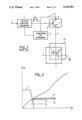
To obtain this charge current as a function of the video signal, it is proposed, notably when the control circuits are integrated into the LCD panel, to use a column driver transistor, the gate of which receives a control pulse as a function of the video signal sample. To illustrate this case, FIG. 1 shows the schematic diagram of a known control for an active matrix LCD panel symbolized by a column cl, a line L, a picture element P, the counter-electrode CE and a line selection thin-film transistor.
More specifically, it has been proposed, as shown in FIG. 1, to use a column control circuit comprising a voltage-duration converter 1 which receives the video signal sample E at one of its inputs and a voltage gradient coming from a gradient, generator 2 at its other input. At output, this converter delivers a pulse I, the duration t of which expresses the amplitude of the video signal sample at input. This pulse I is sent to the gate g of a driver field-effect transistor 3. One of the electrodes, or drain d in the embodiment shown, of this field-effect transistor 3 receives a voltage gradient coming from the generator 2. Its other electrode, or source S, is connected to the column bus considered. With the above-described circuit, so long as the voltage Vgs of the transistor 3 remains greater than its threshold voltage Vt, the signal on the source s follows the changes in the voltage gradient applied to the drain d, and the capacitor C, which represents the equivalent capacitance of the column, namely the liquid crystal capacitance, the unwanted capacitances of the picture element P control transistors and the intersection capacitance of the buses, gets charged. As soon as the voltage Vgs becomes smaller than the threshold voltage Vt, the transistor 3 goes off and the signal at the column keeps, as its value, the value of the voltage charged in the capacitor C. Thus, at each column cl, there is obtained a voltage which is, for example, proportional to the width of the control pulse I of the transistor 3.
In this circuit, the pulse I obtained at output of the converter 1 does not have a steep-sloped descending edge The result thereof is that the transistor 3 goes off at an instant depending on the value of the conduction threshold. Consequently, the capacitor charging voltage changes with the shifting of the threshold. Indeed, the conduction threshold gets shifted through the electrical stress undergone by the field-effect transistor 3 used to switch-over the column. This stress may be defined as the product of the gate-source voltage by the duration in which the voltage is applied. Thus, this stress is a function of the value of the input signal and, hence, of the video signal since the duration of the pulse is a function of the video signal. To illustrate this problem, FIG. 2 shows the pulse I, the voltage gradient and the column voltages V1 and V2 obtained respectively with threshold voltages T1 and T2. It is seen that the raising of the threshold voltage of the transistor tends to reduce the column voltage Vsg. Thus, it can be seen that a low value of the video signal sample generates a gate-source voltage stress which is smaller than the stress generated by a high value of the video signal sample, as shown schematically by A and B in FIG. 3. In the former case, the shift in the threshold voltage will therefore be smaller. The result thereof is a non-uniform shift in the threshold voltages of the different column switch-over transistors, leading to a non-uniformity of luminance on the LCD panel.
The present invention, therefore, is aimed at overcoming this drawback by proposing a method for the addressing of each column that prevents the switch-over threshold of the transistor from changing with the video signal samples.
The present invention is also aimed at proposing a method for the addressing of each column that enables the creation of conditions such that the gate-source stress of the transistor is, on an average, independent of the video signal sample applied to the column.
SUMMARY OF THE INVENTION
Consequently, the present invention is also aimed at proposing a method for the addressing of each column of a matrix type LCD panel consisting in the production of a pulse to control a driver transistor of said column, said pulse having a duration determined by the value of the video signal sample at input, said pulse acting on the conduction state of said transistor to connect said column to a supply terminal where a voltage gradient develops, wherein two pulse durations, the sum of which is predetermined, are alternated and wherein, in order that a given value of a video signal sample may produce the same optical effect from one period to the next one, differentiated excitation voltages are applied to at least one of the electrodes sandwiching the liquid crystal layer, namely said column and its counter-electrode.
According to a particular embodiment, before conversion, the video signal is inverted periodically so that, after conversion, there is obtained a pulse with a duration t during a first period and a pulse with a duration T-t during a second period, T being the duration of the period.
Furthermore, when an AC voltage is applied periodically to the counter-electrode, the same voltage gradient is applied at each period.
However, when a fixed voltage is applied to the counter-electrode, the voltage gradient is shifted symmetrically at each period in relation to the fixed voltage so that a gradient varying between V and V' is applied during a first period and a gradient varying between -V' and -V is applied during a second period.
With this method, the mean value of the gate-source stresses is constant. Thus, the shift in the threshold voltages of the transistors controlling the columns is also constant, and this results in a uniform visual degradation.
However, according to another characteristic of the invention, to overcome this constant shift from the normal of the voltages on the columns, a DC shift voltage, compensating for the mean shift in the threshold voltages of the switch-over transistors, is applied to the counter-electrode.
BACKGROUND OF THE INVENTION
Other features and advantages of the present invention shall appear from the following description of different embodiments, said description being made with reference to the appended drawings, in which:
FIG. 1, already described, is a block diagram of a control circuit of a column of a prior art active matrix LCD panel;
FIG. 2 is a curve giving the voltage as a function of time, explaining the problems due to the stress of the switch-over transistor in the circuit of FIG. 1;
FIG. 3 represents two schematic curves showing the stress as a function of the voltage of the video sample;
FIG. 4 is a block diagram of a control circuit for the implementation of the method of the present invention when the AC voltage is applied to the counter-electrode;
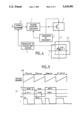
FIG. 5 is a timing diagram explaining the working of the present invention, and
FIG. 6 is a simplified diagram explaining the working of the present invention in the case of an active matrix LCD panel, the counter-electrode of which is at a fixed potential.
To simplify the description, the same references are repeated for the same elements in the figures.
DESCRIPTION OF PREFERRED EMBODIMENTS
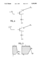
FIG. 4 shows an active matrix LCD panel. This panel has been represented schematically by a single picture element or pixel P at the intersection between a column bus cl and a line bus L. In the embodiment shown, the line L/column c1 coupling is achieved by a thin-film transistor (TFT) T which receives, at its gate, the voltage applied to the line L and, at an electrode, the voltage applied to the column. The other electrode is connected to the electrode of the liquid crystal forming the capacitor C with the counter-electrode CE. The liquid crystal is therefore equivalent to a capacitor C with a resistor (not shown). In the embodiment of FIG. 4, the counter-electrode CE receives an AC voltage coming from a square-wave voltage generator 4. As shown in FIG. 5, the voltage of the counter-electrode CE goes alternately to a level, for example, of five volts for a first period and then to a level of, for example, 0 volt for a second period. Moreover, like the column control circuit of FIG. 1, the column control circuit includes a voltage-duration converter 1 which receives a video signal sample at input and, at another input, a gradient coming from a gradient generator 2. In accordance with the present invention, the video signal sample E comes from a circuit 5 that complements the video signal. The circuit 5 is commanded by the square-wave voltage generator 4 so as to apply the video signal itself during a first period and the complement of the video signal during a second period. Thus, at output of the voltage-duration converter 1, a pulse I is obtained, the duration of which is a function of the amplitude of the video signal, namely a pulse I having, for example, a duration t during the first period and a duration T-t during the second period, T representing the duration of the period, i.e. preferably a frame duration. More generally, the alternation of the two pulse durations is equal to a predetermined sum.
With the above circuit, when the pulse has a duration t, a voltage V' as shown in FIG. 5 is obtained at the source s of the transistor 3. In this case, the voltage at the terminals of the liquid crystal cell is equal to (5 volts-V') in the embodiment shown and corresponds to a high voltage enabling, for example, the display of the black. During the second period, the pulse I has a duration T-t and corresponds to a voltage V on the source. In this case, the voltage at the terminals of the liquid crystal cell becomes equal to 0-V: this voltage is also a high voltage corresponding to the display of the black. As shown in FIG. 5, the square-wave voltage between 0 and 5 V as well as the voltages V and V' are chosen in such a way that (5-V')=(V-0). A null mean voltage is therefore applied to the terminals of the liquid crystal cell. The same conclusions would be obtained for the display of the white or gray levels.
In practice, the threshold voltages of the control transistors of the different lines undergo a shift such that the voltages corresponding respectively to the white and black levels are no longer V and V'but generally V-DV and V'-DV. To overcome these shifts in voltages at the picture element, according to the present invention a shift voltage of the same level is applied to the counter-electrode. However, this compensation can also be achieved at other places, notably by decoding the gradient, or at the video signal itself.
Referring to FIG. 6, we shall now describe an embodiment of the addressing method according to the present invention when the counter-electrode CE receives a fixed voltage, for example a voltage of 0 volts. In accordance with the present invention, in this case, not only is the video signal E alternately transmitted or complemented at each period, but the gradient applied to one of the electrodes of the switch-over transistor is shifted in voltage at each period. Thus, we apply either a gradient varying, for example between 0 and 5 volts during a first period or a gradient varying between -5 volts and 0 volt during a second period, as shown in FIG. 5 which concerns an example of the encoding of a black picture element. In the embodiment shown, the pulse applied to the gate of the transistor 3 has a duration which corresponds to a maximum stress. The voltage at the terminals of the pixel P is therefore equal to 5 volts (maximum value of the gradient) -0 volt (voltage applied to the counter-electrode) giving 5 volts which corresponds to a minimum luminance of the picture element. During the second period, the pulse applied to the gate of the transistor 3 has a duration T-to corresponding to a minimum stress. The voltage at the terminals of the pixel is equal to -5 volts (minimum value of the gradient) -0 volts (value of the voltage of the counter-electrode) giving -5 volts. The luminance of the picture element is again the minimum in this case. Thus, in matching the variations in voltage of the gradient applied to the electrode of the transistor 3, it is possible to make the stress applied to all the transistors of the control circuit uniform by reversing the video signal from one period to another.
The two embodiments described above have been given by way of example and are not restrictive as regards the scope of the claims.

Claims (7)

What is claimed is:
1. A method for the addressing of each column of a matrix type LCD panel consisting in the production of a pulse segment as a function of a video signal wherein said pulse segment functions to control a driver transistor of said column, said pulse segment having a duration determined by the value of an input video signal sample, said pulse segment acting on said transistor to cause said transistor to conduct in order to connect said column to a voltage gradient supply terminal, wherein said pulse segment includes two pulse durations, the sum of which is a frame duration, and said two pulse segments are alternated and wherein, in order that a given value of a video signal sample may produce the same optical effect from one period to the next one, differentiated excitation voltages are applied to at least one of two electrodes sandwiching the crystal layer, said crystal layer and said electrodes including said column and its counter-electrode.
2. An addressing method according to claim 1 wherein, before conversion, the video signal is inverted periodically so that, after conversion, there is obtained a pulse with a duration t during a first period and a pulse with a duration T-t during a second period, T being the duration of the period.
3. A method according to claim 1 wherein, when an AC voltage is applied periodically to the counter-electrode, the same voltage gradient is applied at each period.
4. A method according to claim 1 wherein, when a fixed voltage is applied to the counter-electrode, the voltage gradient is shifted symmetrically at each period in relation to the fixed voltage so that a gradient varying between V and V' is applied during a first period and a gradient varying between -V' and -V is applied during a second period.
5. A method according to claim 2, wherein the period T corresponds to a frame.
6. A method according to claim 1, wherein the LCD panel is an active matrix panel.
7. A method according to claim 1, wherein a DC shift voltage, compensating for the mean shift in the threshold voltages of the switch-over transistors, is applied to the counter-electrode.
US08/047,360 1989-12-28 1993-04-19 Method for addressing each column of a matrix type LCD panel Expired - Lifetime US5319381A (en)

Priority Applications (1)

Application Number Priority Date Filing Date Title
US08/047,360 US5319381A (en) 1989-12-28 1993-04-19 Method for addressing each column of a matrix type LCD panel

Applications Claiming Priority (4)

Application Number Priority Date Filing Date Title
FR8917312A FR2656757B1 (en) 1989-12-28 1989-12-28 METHOD FOR ADDRESSING EACH COLUMN OF A MATRIX TYPE LCD SCREEN.
FR8917312 1989-12-28
US63019390A 1990-12-19 1990-12-19
US08/047,360 US5319381A (en) 1989-12-28 1993-04-19 Method for addressing each column of a matrix type LCD panel

Related Parent Applications (1)

Application Number Title Priority Date Filing Date
US63019390A Continuation 1989-12-28 1990-12-19

Publications (1)

Publication Number Publication Date
US5319381A true US5319381A (en) 1994-06-07

Family

ID=9389059

Family Applications (1)

Application Number Title Priority Date Filing Date
US08/047,360 Expired - Lifetime US5319381A (en) 1989-12-28 1993-04-19 Method for addressing each column of a matrix type LCD panel

Country Status (6)

Country Link
US (1) US5319381A (en)
EP (1) EP0435750B1 (en)
JP (1) JP3034612B2 (en)
AT (1) ATE135129T1 (en)
DE (1) DE69025736D1 (en)
FR (1) FR2656757B1 (en)

Cited By (5)

* Cited by examiner, † Cited by third party
Publication number Priority date Publication date Assignee Title
US6064364A (en) * 1993-12-27 2000-05-16 Sharp Kabushiki Kaisha Image display scanning circuit with outputs from sequentially switched pulse signals
US6137466A (en) * 1997-11-03 2000-10-24 Motorola, Inc. LCD driver module and method thereof
US6215533B1 (en) * 1996-05-17 2001-04-10 Sharp Kabushiki Kaisha Ferroelectric liquid crystal driving using square wave and non-square wave signals
US6310599B1 (en) 1995-12-22 2001-10-30 Cirrus Logic, Inc. Method and apparatus for providing LCD panel protection in an LCD display controller
WO2007034353A3 (en) * 2005-09-19 2008-01-03 Koninkl Philips Electronics Nv Active-matrix display devices and methods of driving the same

Families Citing this family (8)

* Cited by examiner, † Cited by third party
Publication number Priority date Publication date Assignee Title
WO1992007352A1 (en) * 1990-10-19 1992-04-30 Thomson S.A. Control circuit for matrix-type readout devices and signal decoder for such circuit
GB9217336D0 (en) * 1992-08-14 1992-09-30 Philips Electronics Uk Ltd Active matrix display devices and methods for driving such
JPH06314080A (en) * 1993-04-14 1994-11-08 Internatl Business Mach Corp <Ibm> Liquid-crystal display device
JP3470440B2 (en) * 1995-02-28 2003-11-25 ソニー株式会社 Lamp signal generation method, lamp signal generation device, liquid crystal driving device, and liquid crystal display device
FR2787910B1 (en) * 1998-12-23 2001-03-16 Sextant Avionique LIQUID CRYSTAL SCREEN CONTROL CIRCUIT
US6657609B2 (en) * 2001-09-28 2003-12-02 Koninklijke Philips Electronics N.V. Liquid crystal displays with reduced flicker
KR100605763B1 (en) * 2005-01-18 2006-08-01 엘지전자 주식회사 Plasma Display Panel Driving Apparatus And Method
JP4810910B2 (en) * 2005-07-26 2011-11-09 エプソンイメージングデバイス株式会社 Electro-optical device, driving method, and electronic apparatus

Citations (11)

* Cited by examiner, † Cited by third party
Publication number Priority date Publication date Assignee Title
GB2135099A (en) * 1983-01-21 1984-08-22 Citizen Watch Co Ltd Drive circuit for matrix display device
US4525710A (en) * 1982-02-16 1985-06-25 Seiko Instruments & Electronics Ltd. Picture display device
US4591848A (en) * 1982-04-01 1986-05-27 Seiko Epson Corporation Matrix panel with an active driving system
EP0199361A2 (en) * 1985-04-26 1986-10-29 Matsushita Electric Industrial Co., Ltd. Driver circuit for liquid crystal display
US4635127A (en) * 1982-12-21 1987-01-06 Citizen Watch Company Limited Drive method for active matrix display device
US4710768A (en) * 1983-10-13 1987-12-01 Sharp Kabushiki Kaisha Liquid crystal display with switching transistor for each pixel
GB2204174A (en) * 1987-04-23 1988-11-02 Seiko Instr Inc Electro-optical modulator
US4795239A (en) * 1985-08-29 1989-01-03 Canon Kabushiki Kaisha Method of driving a display panel
EP0298255A1 (en) * 1987-06-04 1989-01-11 Seiko Epson Corporation Circuit for driving a liquid crystal display panel
US4917470A (en) * 1985-01-14 1990-04-17 Canon Kabushiki Kaisha Driving method for liquid crystal cell and liquid crystal apparatus
US5018841A (en) * 1985-12-25 1991-05-28 Canon Kabushiki Kaisha Driving method for optical modulation device

Patent Citations (12)

* Cited by examiner, † Cited by third party
Publication number Priority date Publication date Assignee Title
US4525710A (en) * 1982-02-16 1985-06-25 Seiko Instruments & Electronics Ltd. Picture display device
US4591848A (en) * 1982-04-01 1986-05-27 Seiko Epson Corporation Matrix panel with an active driving system
US4635127A (en) * 1982-12-21 1987-01-06 Citizen Watch Company Limited Drive method for active matrix display device
GB2135099A (en) * 1983-01-21 1984-08-22 Citizen Watch Co Ltd Drive circuit for matrix display device
US4710768A (en) * 1983-10-13 1987-12-01 Sharp Kabushiki Kaisha Liquid crystal display with switching transistor for each pixel
US4917470A (en) * 1985-01-14 1990-04-17 Canon Kabushiki Kaisha Driving method for liquid crystal cell and liquid crystal apparatus
EP0199361A2 (en) * 1985-04-26 1986-10-29 Matsushita Electric Industrial Co., Ltd. Driver circuit for liquid crystal display
US4734692A (en) * 1985-04-26 1988-03-29 Matsushita Electric Industrial Co., Ltd. Driver circuit for liquid crystal display
US4795239A (en) * 1985-08-29 1989-01-03 Canon Kabushiki Kaisha Method of driving a display panel
US5018841A (en) * 1985-12-25 1991-05-28 Canon Kabushiki Kaisha Driving method for optical modulation device
GB2204174A (en) * 1987-04-23 1988-11-02 Seiko Instr Inc Electro-optical modulator
EP0298255A1 (en) * 1987-06-04 1989-01-11 Seiko Epson Corporation Circuit for driving a liquid crystal display panel

Cited By (5)

* Cited by examiner, † Cited by third party
Publication number Priority date Publication date Assignee Title
US6064364A (en) * 1993-12-27 2000-05-16 Sharp Kabushiki Kaisha Image display scanning circuit with outputs from sequentially switched pulse signals
US6310599B1 (en) 1995-12-22 2001-10-30 Cirrus Logic, Inc. Method and apparatus for providing LCD panel protection in an LCD display controller
US6215533B1 (en) * 1996-05-17 2001-04-10 Sharp Kabushiki Kaisha Ferroelectric liquid crystal driving using square wave and non-square wave signals
US6137466A (en) * 1997-11-03 2000-10-24 Motorola, Inc. LCD driver module and method thereof
WO2007034353A3 (en) * 2005-09-19 2008-01-03 Koninkl Philips Electronics Nv Active-matrix display devices and methods of driving the same

Also Published As

Publication number Publication date
JP3034612B2 (en) 2000-04-17
EP0435750A1 (en) 1991-07-03
FR2656757B1 (en) 1992-03-20
ATE135129T1 (en) 1996-03-15
FR2656757A1 (en) 1991-07-05
JPH04136893A (en) 1992-05-11
DE69025736D1 (en) 1996-04-11
EP0435750B1 (en) 1996-03-06

Similar Documents

Publication Publication Date Title
US6590552B1 (en) Method of driving liquid crystal display device
US5398043A (en) Driving method for a display device
KR100870487B1 (en) Method and apparatus for driving liquid crystal display for wide viewing angle
US6359608B1 (en) Method and apparatus for driving flat screen displays using pixel precharging
EP0678849B1 (en) Active matrix display device with precharging circuit and its driving method
US5940057A (en) Method and apparatus for eliminating crosstalk in active matrix liquid crystal displays
KR100361465B1 (en) Method of Driving Liquid Crystal Panel and Apparatus thereof
US5748171A (en) Liquid crystal display
US5319381A (en) Method for addressing each column of a matrix type LCD panel
US5598177A (en) Driving apparatus and method for an active matrix type liquid crystal display apparatus
JPH05165431A (en) Driving method for liquid crystal display device
US4909602A (en) Liquid crystal display and method of driving the same
KR100366476B1 (en) method for optimised addressing of a liquid crystal display and device for implementing same
KR20050066139A (en) Driving method of in-plane-switching mode lcd
JP2730286B2 (en) Driving method of display device
EP1611564B1 (en) Active matrix displays and contrast control method
US6344842B1 (en) Liquid crystal display device and a driving method therefor
EP0526713B1 (en) Liquid crystal display with active matrix
US6069603A (en) Method of driving a matrix display device
KR100552278B1 (en) Liquid crystal display that varies the gate signal
JP3160143B2 (en) Liquid crystal display
US20030112211A1 (en) Active matrix liquid crystal display devices
JP2590229B2 (en) Liquid crystal display
KR100965824B1 (en) Liquid Crystal Display and Driving Method
JPH09179098A (en) Display device

Legal Events

Date Code Title Description
STPP Information on status: patent application and granting procedure in general

Free format text: APPLICATION UNDERGOING PREEXAM PROCESSING

AS Assignment

Owner name: THOMSON CONSUMER ELECTRONICS, FRANCE

Free format text: ASSIGNMENT OF ASSIGNORS INTEREST;ASSIGNORS:MOUREY, BRUNO;BENOIT, ERIC;DUPONT, ANTOINE;REEL/FRAME:006887/0869

Effective date: 19901227

FPAY Fee payment

Year of fee payment: 4

FEPP Fee payment procedure

Free format text: PAYOR NUMBER ASSIGNED (ORIGINAL EVENT CODE: ASPN); ENTITY STATUS OF PATENT OWNER: LARGE ENTITY

FPAY Fee payment

Year of fee payment: 8

SULP Surcharge for late payment

Year of fee payment: 7

FPAY Fee payment

Year of fee payment: 12