US5276324A - Composite scanning tunneling microscope - Google Patents
Composite scanning tunneling microscope Download PDFInfo
- Publication number
- US5276324A US5276324A US07/921,130 US92113092A US5276324A US 5276324 A US5276324 A US 5276324A US 92113092 A US92113092 A US 92113092A US 5276324 A US5276324 A US 5276324A
- Authority
- US
- United States
- Prior art keywords
- tunneling microscope
- objective optical
- scanner
- optical system
- scanning tunneling
- Prior art date
- Legal status (The legal status is an assumption and is not a legal conclusion. Google has not performed a legal analysis and makes no representation as to the accuracy of the status listed.)
- Expired - Fee Related
Links
Images


Classifications
-
- G—PHYSICS
- G01—MEASURING; TESTING
- G01Q—SCANNING-PROBE TECHNIQUES OR APPARATUS; APPLICATIONS OF SCANNING-PROBE TECHNIQUES, e.g. SCANNING PROBE MICROSCOPY [SPM]
- G01Q60/00—Particular types of SPM [Scanning Probe Microscopy] or microscopes; Essential components thereof
- G01Q60/10—STM [Scanning Tunnelling Microscopy] or apparatus therefor, e.g. STM probes
- G01Q60/16—Probes, their manufacture, or their related instrumentation, e.g. holders
-
- B—PERFORMING OPERATIONS; TRANSPORTING
- B82—NANOTECHNOLOGY
- B82Y—SPECIFIC USES OR APPLICATIONS OF NANOSTRUCTURES; MEASUREMENT OR ANALYSIS OF NANOSTRUCTURES; MANUFACTURE OR TREATMENT OF NANOSTRUCTURES
- B82Y35/00—Methods or apparatus for measurement or analysis of nanostructures
-
- G—PHYSICS
- G01—MEASURING; TESTING
- G01Q—SCANNING-PROBE TECHNIQUES OR APPARATUS; APPLICATIONS OF SCANNING-PROBE TECHNIQUES, e.g. SCANNING PROBE MICROSCOPY [SPM]
- G01Q10/00—Scanning or positioning arrangements, i.e. arrangements for actively controlling the movement or position of the probe
- G01Q10/04—Fine scanning or positioning
-
- G—PHYSICS
- G01—MEASURING; TESTING
- G01Q—SCANNING-PROBE TECHNIQUES OR APPARATUS; APPLICATIONS OF SCANNING-PROBE TECHNIQUES, e.g. SCANNING PROBE MICROSCOPY [SPM]
- G01Q30/00—Auxiliary means serving to assist or improve the scanning probe techniques or apparatus, e.g. display or data processing devices
- G01Q30/02—Non-SPM analysing devices, e.g. SEM [Scanning Electron Microscope], spectrometer or optical microscope
- G01Q30/025—Optical microscopes coupled with SPM
-
- G—PHYSICS
- G02—OPTICS
- G02B—OPTICAL ELEMENTS, SYSTEMS OR APPARATUS
- G02B21/00—Microscopes
- G02B21/0004—Microscopes specially adapted for specific applications
- G02B21/002—Scanning microscopes
-
- Y—GENERAL TAGGING OF NEW TECHNOLOGICAL DEVELOPMENTS; GENERAL TAGGING OF CROSS-SECTIONAL TECHNOLOGIES SPANNING OVER SEVERAL SECTIONS OF THE IPC; TECHNICAL SUBJECTS COVERED BY FORMER USPC CROSS-REFERENCE ART COLLECTIONS [XRACs] AND DIGESTS
- Y10—TECHNICAL SUBJECTS COVERED BY FORMER USPC
- Y10S—TECHNICAL SUBJECTS COVERED BY FORMER USPC CROSS-REFERENCE ART COLLECTIONS [XRACs] AND DIGESTS
- Y10S977/00—Nanotechnology
- Y10S977/84—Manufacture, treatment, or detection of nanostructure
- Y10S977/849—Manufacture, treatment, or detection of nanostructure with scanning probe
- Y10S977/86—Scanning probe structure
- Y10S977/868—Scanning probe structure with optical means
- Y10S977/869—Optical microscope
Definitions
- the present invention relates to a scanning tunneling microscope. More particularly, the present invention relates to a composite scanning tunneling microscope, in which a tunneling microscope is combined with an optical microscope.
- a tunneling microscope as disclosed in the above Laid-open Patent has a probe 2 for tunnel current detection unitedly fixed on an objective lens 1, which detects a very weak electric current from the probe 2 through a conductive layer 3.
- the above Laid-open Patent describes another tunneling microscope as shown in FIG. 7, in which a glass plate 5, which does not affect an optical image, is disposed between an objective lens 1 and a sample 4 and in which a probe 6 is attached to the glass plate 5.
- the glass plate 5 is fixed to a lens barrel supporting the objective lens 1 or to a housing of the microscope.
- the incorporation of the probe with the objective lens is not easy in position adjustment to set the probe at a position where the tip of probe is located in a depth of focus of the optical microscope, which leads to difficulties in exchange of probe.
- a tunneling microscope of the present invention comprises a first objective optical system for collimating an optical flux from a sample, a second objective optical system for condensing the optical flux thus collimated, and a transparent member disposed between the first and the second objective optical systems.
- a through hole is perforated along an optical axis in the center of the first objective optical system.
- a tube scanner member has a probe for detecting a tunnel current, which is disposed at one end of the scanner. The tube scanner member passes through the hole of the first objective optical system without a contact therewith. The other end of the tube scanner member is fixed to the transparent member.
- the tube scanner member fixed to the transparent member is separate from and independent of an optical microscope, so that a tunnel current may stably be detected without influences on the probe from vibrations of the optical microscope.
- the first and the second objective optical systems are displaceable independently of the tube scanner member, so that the tip of probe may readily be made coincident with the depth of focus of the objective optical systems by moving them along an optical axis thereof.
- the tube scanner member disposed in the center of the objective optical systems may be formed small in outer diameter, and therefore a response of probe scanning may be improved.
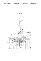
- FIG. 1 is a sectional view to show a schematic structure of a tunneling microscope in an embodiment according to the present invention
- FIG. 2 is a sectional view of main part of FIG. 1;
- FIG. 3 is a perspective view to show a tube scanner member
- FIG. 4 is a perspective view of a transparent member
- FIG. 5 is a perspective view to show a modification of the transparent member
- FIG. 6 is a sectional view of main part of a conventional composite scanning tunneling microscope.
- FIG. 7 is a sectional view of main part of another conventional composite scanning tunneling microscope.
- FIG. 1 shows an embodiment of a composite scanning tunneling microscope, which is composed of a scanning tunneling microscope 10 and an optical microscope 30.
- the scanning tunneling microscope 10 is supported by a support plate 16 on a column 15 standing on a vibration isolating table 12, which may observe unevenness on a surface of sample 50 by scanning the sample 50 with a probe 20.
- the optical microscope 30 is provided for simultaneous observation of the tip of probe 20 and of the surface of a sample, which is supported by a support plate 18 on a column 17 standing on the vibration isolating table 12.
- the optical microscope 30 is provided with an objective optical system 32 for forming a magnified image 51 of the sample 50 on an optical axis thereof.
- the objective optical system 32 comprises a first objective optical system 33 for collimating an optical flux from the sample 50 and a second objective optical system 34 for forming an image 51 while condensing the optical flux collimated.
- the first and the second objective optical systems 33, 34 are respectively represented by a single lens in FIG. 1, they are usually composed of a plurality of lenses.
- There is an unrepresented mechanism provided for moving the objective optical system 32 along the optical axis to align the probe 20 in the depth of focus of the objective optical system.
- a drop light illumination device is incorporated in the optical microscope 30.
- the drop light illumination device is provided with a half mirror 35 disposed on the optical axis between the magnified image 51 and the second objective optical system 34, and with an illumination light source 36.
- a circular through hole 33a is perforated in the first objective optical system 33 around the optical axis, and a tube scanner member 21 passes through the hole 33a without a contact with the first objective optical system 33.
- the tube scanner member 21 comprises a cylindrical piezoelectric ceramics 40, a holder 41 supporting the probe 20, and an electrode group attached to an outer circumference and an inner circumference of the piezoelectric ceramics 40, as shown in FIGS. 2 and 3.
- the electrode group consists of four plate electrodes 43a, 43b, 43c, 43d disposed outside the tube scanner member 21, and a ground electrode 44 disposed inside the member 21. Electrode wires 45a, 45b, 45c, 45d and a ground wire 46 are respectively connected to the electrodes 43a, 43b, 43c, 43d and to the ground electrode 44, and withdrawn therefrom.
- a tunnel current signal wire 47 is withdrawn from the probe 20 in order to take out a tunnel current.
- a circular parallel plain glass 25 is positioned between the first and the second objective optical systems 33, 34 to cross the collimated optical flux.
- the parallel plain glass 25 is fixed in a circular opening 16a formed in the support plate 16.
- a through hole 26 is formed in the center of the parallel plain glass 25 to hold the upper portion of the tube scanner member 21.
- a plurality of transparent electrodes 48 are coated radially from the periphery of the through hole 26 on the both front and back faces of the tube scanner member.
- the transparent electrodes 48 electrically connect the electrode wires 45a-45b, the ground wire 46, and the tunnel current signal wire 47 to an unrepresented control circuit of the tunneling microscope.
- the transparent electrodes may be replaced by ordinary wires. The use of ordinary wires might cause a slight loss in quantity of light, but the loss will not affect an observation by the optical microscope.
- the parallel plain glass 25 itself may be replaced by a circular support frame 60 as shown in FIG. 5.
- the support frame 60 has an inside annular member 61, an outside annular member 62, and four radial arms 63 connecting between the annular members 61, 62.
- preferable electrical connections to the electrode wires 45a-45d, to the ground wire 46, and to the tunnel current signal wire 47 are wiring with wires along the four arms 63.
- the tunneling microscope and the optical microscope are independently supported on the vibration isolating table 12, so that vibrations may be minimized to transmit from the optical microscope to the tunneling microscope, enabling to observe a fine constitution of surface of sample in a resolving power of atom based on the detection of tunnel current.
- a simple operation can adjust the optical microscope so as to bring the tip of probe within the focus of depth, because the objective optical system and the tube scanner member are so arranged as to be movable relative to each other along the optical axis.
- an outer diameter of the tube scanner member may be formed smaller, and the tunneling microscope has a good response upon scanning of sample with the probe.
Landscapes
- Physics & Mathematics (AREA)
- General Physics & Mathematics (AREA)
- Health & Medical Sciences (AREA)
- General Health & Medical Sciences (AREA)
- Nuclear Medicine, Radiotherapy & Molecular Imaging (AREA)
- Radiology & Medical Imaging (AREA)
- Chemical & Material Sciences (AREA)
- Analytical Chemistry (AREA)
- Engineering & Computer Science (AREA)
- Nanotechnology (AREA)
- Optics & Photonics (AREA)
- Crystallography & Structural Chemistry (AREA)
- Measurement Of Length, Angles, Or The Like Using Electric Or Magnetic Means (AREA)
Applications Claiming Priority (2)
| Application Number | Priority Date | Filing Date | Title |
|---|---|---|---|
| JP3199461A JPH0540009A (ja) | 1991-08-08 | 1991-08-08 | 走査型トンネル顕微鏡 |
| JP3-199461 | 1991-08-08 |
Publications (1)
| Publication Number | Publication Date |
|---|---|
| US5276324A true US5276324A (en) | 1994-01-04 |
Family
ID=16408190
Family Applications (1)
| Application Number | Title | Priority Date | Filing Date |
|---|---|---|---|
| US07/921,130 Expired - Fee Related US5276324A (en) | 1991-08-08 | 1992-07-29 | Composite scanning tunneling microscope |
Country Status (3)
| Country | Link |
|---|---|
| US (1) | US5276324A (de) |
| EP (1) | EP0527601A1 (de) |
| JP (1) | JPH0540009A (de) |
Cited By (14)
| Publication number | Priority date | Publication date | Assignee | Title |
|---|---|---|---|---|
| US5440920A (en) * | 1994-02-03 | 1995-08-15 | Molecular Imaging Systems | Scanning force microscope with beam tracking lens |
| US5463897A (en) * | 1993-08-17 | 1995-11-07 | Digital Instruments, Inc. | Scanning stylus atomic force microscope with cantilever tracking and optical access |
| US5508517A (en) * | 1991-03-15 | 1996-04-16 | Nikon Corporation | Scanning probe type microscope apparatus |
| US5515719A (en) * | 1994-05-19 | 1996-05-14 | Molecular Imaging Corporation | Controlled force microscope for operation in liquids |
| USRE35317E (en) * | 1991-07-26 | 1996-08-27 | The Arizona Board Of Regents | Potentiostatic preparation of molecular adsorbates for scanning probe microscopy |
| US5612491A (en) * | 1994-05-19 | 1997-03-18 | Molecular Imaging Corporation | Formation of a magnetic film on an atomic force microscope cantilever |
| US5621210A (en) * | 1995-02-10 | 1997-04-15 | Molecular Imaging Corporation | Microscope for force and tunneling microscopy in liquids |
| US5753814A (en) * | 1994-05-19 | 1998-05-19 | Molecular Imaging Corporation | Magnetically-oscillated probe microscope for operation in liquids |
| US5861624A (en) * | 1997-08-22 | 1999-01-19 | Park Scientific Instruments | Atomic force microscope for attachment to optical microscope |
| US5866805A (en) * | 1994-05-19 | 1999-02-02 | Molecular Imaging Corporation Arizona Board Of Regents | Cantilevers for a magnetically driven atomic force microscope |
| US5952657A (en) * | 1997-08-22 | 1999-09-14 | Thermo Microscopes, Corp. | Atomic force microscope with integrated optics for attachment to optical microscope |
| US6545263B2 (en) * | 1998-09-14 | 2003-04-08 | Carl Zeiss Jena Gmbh | Scanning probe microscope with probe integrated in an optical system |
| US20050012990A1 (en) * | 2003-07-15 | 2005-01-20 | Nikon Corporation | Microscope |
| US10884227B2 (en) | 2016-11-10 | 2021-01-05 | The Trustees Of Columbia University In The City Of New York | Rapid high-resolution imaging methods for large samples |
Families Citing this family (5)
| Publication number | Priority date | Publication date | Assignee | Title |
|---|---|---|---|---|
| CN100420934C (zh) * | 2002-11-14 | 2008-09-24 | 南开大学 | 一种近场扫描光学显微镜定位扫描成像方法 |
| EP2120036B1 (de) * | 2008-05-16 | 2012-07-18 | Mitutoyo Corporation | Messsonde mit einem oder mehreren Stützelementen für ein Messinstrument |
| EP2120037B1 (de) * | 2008-05-16 | 2017-01-25 | Mitutoyo Corporation | Messsonde für ein Scanmikroskop und Betriebsverfahren dafür |
| EP2163906B1 (de) | 2008-09-16 | 2014-02-26 | Mitutoyo Corporation | Verfahren zur Bewegungserkennung einer Messsonde und Messinstrument |
| EP2211187B1 (de) | 2009-01-14 | 2013-10-02 | Mitutoyo Corporation | Verfahren zur Betätigung eines Systems, Vorrichtung zur Modifizierung eines Steuersignals zur Betätigung eines Systems und Verfahren zum Abstimmen einer solchen Vorrichtung |
Citations (6)
| Publication number | Priority date | Publication date | Assignee | Title |
|---|---|---|---|---|
| EP0331148A2 (de) * | 1988-03-04 | 1989-09-06 | Kabushiki Kaisha Toshiba | Mikroskop |
| JPH0216403A (ja) * | 1988-03-04 | 1990-01-19 | Toshiba Corp | 顕微鏡装置 |
| EP0405973A1 (de) * | 1989-06-29 | 1991-01-02 | Seiko Instruments Inc. | Raster-Tunnel-Mikroskop in Kombination mit einem optischen Mikroskop |
| EP0406413A1 (de) * | 1987-08-12 | 1991-01-09 | Olympus Optical Co., Ltd. | Tunnel-abtastmikroskop |
| EP0421354A2 (de) * | 1989-10-02 | 1991-04-10 | Olympus Optical Co., Ltd. | Raster-Tunnel-Mikroskop |
| US5206702A (en) * | 1989-10-09 | 1993-04-27 | Olympus Optical Co., Ltd. | Technique for canceling the effect of external vibration on an atomic force microscope |
-
1991
- 1991-08-08 JP JP3199461A patent/JPH0540009A/ja active Pending
-
1992
- 1992-07-29 US US07/921,130 patent/US5276324A/en not_active Expired - Fee Related
- 1992-08-07 EP EP92307221A patent/EP0527601A1/de not_active Ceased
Patent Citations (8)
| Publication number | Priority date | Publication date | Assignee | Title |
|---|---|---|---|---|
| EP0406413A1 (de) * | 1987-08-12 | 1991-01-09 | Olympus Optical Co., Ltd. | Tunnel-abtastmikroskop |
| EP0331148A2 (de) * | 1988-03-04 | 1989-09-06 | Kabushiki Kaisha Toshiba | Mikroskop |
| JPH0216403A (ja) * | 1988-03-04 | 1990-01-19 | Toshiba Corp | 顕微鏡装置 |
| US4914293A (en) * | 1988-03-04 | 1990-04-03 | Kabushiki Kaisha Toshiba | Microscope apparatus |
| EP0405973A1 (de) * | 1989-06-29 | 1991-01-02 | Seiko Instruments Inc. | Raster-Tunnel-Mikroskop in Kombination mit einem optischen Mikroskop |
| EP0421354A2 (de) * | 1989-10-02 | 1991-04-10 | Olympus Optical Co., Ltd. | Raster-Tunnel-Mikroskop |
| US5083022A (en) * | 1989-10-02 | 1992-01-21 | Olympus Optical Co., Ltd. | Scanning tunneling microscope |
| US5206702A (en) * | 1989-10-09 | 1993-04-27 | Olympus Optical Co., Ltd. | Technique for canceling the effect of external vibration on an atomic force microscope |
Non-Patent Citations (2)
| Title |
|---|
| Yasutake et al., "Scanning Tunneling Microscope Combined with Optical Microscope for Large Sample Measurement", Journal of Vacuum Science and Technology A, vol. 8, Jan. 1990, pp. 350-353. |
| Yasutake et al., Scanning Tunneling Microscope Combined with Optical Microscope for Large Sample Measurement , Journal of Vacuum Science and Technology A, vol. 8, Jan. 1990, pp. 350 353. * |
Cited By (20)
| Publication number | Priority date | Publication date | Assignee | Title |
|---|---|---|---|---|
| US5508517A (en) * | 1991-03-15 | 1996-04-16 | Nikon Corporation | Scanning probe type microscope apparatus |
| USRE35317E (en) * | 1991-07-26 | 1996-08-27 | The Arizona Board Of Regents | Potentiostatic preparation of molecular adsorbates for scanning probe microscopy |
| US5463897A (en) * | 1993-08-17 | 1995-11-07 | Digital Instruments, Inc. | Scanning stylus atomic force microscope with cantilever tracking and optical access |
| US5714682A (en) * | 1993-08-17 | 1998-02-03 | Digital Instruments, Inc. | Scanning stylus atomic force microscope with cantilever tracking and optical access |
| US5763767A (en) * | 1994-02-03 | 1998-06-09 | Molecular Imaging Corp. | Atomic force microscope employing beam-tracking |
| US5440920A (en) * | 1994-02-03 | 1995-08-15 | Molecular Imaging Systems | Scanning force microscope with beam tracking lens |
| US5587523A (en) * | 1994-02-03 | 1996-12-24 | Molecular Imaging Corporation | Atomic force microscope employing beam tracking |
| US6134955A (en) * | 1994-05-19 | 2000-10-24 | Molecular Imaging Corporation | Magnetic modulation of force sensor for AC detection in an atomic force microscope |
| US5515719A (en) * | 1994-05-19 | 1996-05-14 | Molecular Imaging Corporation | Controlled force microscope for operation in liquids |
| US5753814A (en) * | 1994-05-19 | 1998-05-19 | Molecular Imaging Corporation | Magnetically-oscillated probe microscope for operation in liquids |
| US5866805A (en) * | 1994-05-19 | 1999-02-02 | Molecular Imaging Corporation Arizona Board Of Regents | Cantilevers for a magnetically driven atomic force microscope |
| US5612491A (en) * | 1994-05-19 | 1997-03-18 | Molecular Imaging Corporation | Formation of a magnetic film on an atomic force microscope cantilever |
| US5621210A (en) * | 1995-02-10 | 1997-04-15 | Molecular Imaging Corporation | Microscope for force and tunneling microscopy in liquids |
| US5861624A (en) * | 1997-08-22 | 1999-01-19 | Park Scientific Instruments | Atomic force microscope for attachment to optical microscope |
| US5952657A (en) * | 1997-08-22 | 1999-09-14 | Thermo Microscopes, Corp. | Atomic force microscope with integrated optics for attachment to optical microscope |
| US6545263B2 (en) * | 1998-09-14 | 2003-04-08 | Carl Zeiss Jena Gmbh | Scanning probe microscope with probe integrated in an optical system |
| US20050012990A1 (en) * | 2003-07-15 | 2005-01-20 | Nikon Corporation | Microscope |
| US7092151B2 (en) | 2003-07-15 | 2006-08-15 | Nikon Corporation | Microscope having a pipette device |
| US10884227B2 (en) | 2016-11-10 | 2021-01-05 | The Trustees Of Columbia University In The City Of New York | Rapid high-resolution imaging methods for large samples |
| US11506877B2 (en) | 2016-11-10 | 2022-11-22 | The Trustees Of Columbia University In The City Of New York | Imaging instrument having objective axis and light sheet or light beam projector axis intersecting at less than 90 degrees |
Also Published As
| Publication number | Publication date |
|---|---|
| JPH0540009A (ja) | 1993-02-19 |
| EP0527601A1 (de) | 1993-02-17 |
Similar Documents
| Publication | Publication Date | Title |
|---|---|---|
| US5276324A (en) | Composite scanning tunneling microscope | |
| US4999495A (en) | Scanning tunneling microscope | |
| US4784481A (en) | Transmitted and/or incident light microscope | |
| EP0253152B1 (de) | Linsenhalterung | |
| US5056886A (en) | Optical switching device | |
| DK147328B (da) | Fremgangsmaade og apparat til anbringelse af et endehylster paa en optisk fiber | |
| JPH03120401A (ja) | 微細表面形状計測装置 | |
| US4096386A (en) | Light reflecting electrostatic electron lens | |
| US5677525A (en) | Ancillary module for making a spatially-resolved measurement of a focus volume | |
| US4697880A (en) | Optical system for providing a collimated light beam | |
| JPH0651204A (ja) | システム顕微鏡 | |
| EP0969484B1 (de) | Aufnahmevorrichtung für Proben | |
| US5483065A (en) | Electron beam microanalyzer | |
| JP3148035B2 (ja) | 機械的に安定な放出銃構体 | |
| US7307784B2 (en) | High-stability optical microscope | |
| US7463414B2 (en) | Microscope | |
| JPH0264401A (ja) | 精密3次元形状測定装置 | |
| US2409328A (en) | Illuminating unit for optical projectors | |
| US5580162A (en) | Lighting device for an observation/image pickup apparatus | |
| JPH02188711A (ja) | レーザ光学装置 | |
| JP5530245B2 (ja) | 複合顕微鏡および複合顕微鏡のケーブル支持装置 | |
| US4948984A (en) | Optical scanning head with objective position measuring and mirrors | |
| JPH02163601A (ja) | 走査型トンネル顕微鏡 | |
| SU915122A1 (ru) | Устройство для сборки анодной диафрагмы с узлом электронного прожектора в электроннолучевых приборах 1 | |
| JP3039934U (ja) | ビデオモジュールを有する顕微鏡 |
Legal Events
| Date | Code | Title | Description |
|---|---|---|---|
| AS | Assignment |
Owner name: NIKON CORPORATION, JAPAN Free format text: ASSIGNMENT OF ASSIGNORS INTEREST.;ASSIGNORS:OHTAKI, TATSURO;OHKUBO, HIDEAKI;MATSUSHIRO, HIROYUKI;REEL/FRAME:006200/0579 Effective date: 19920724 |
|
| FEPP | Fee payment procedure |
Free format text: PAYOR NUMBER ASSIGNED (ORIGINAL EVENT CODE: ASPN); ENTITY STATUS OF PATENT OWNER: LARGE ENTITY |
|
| FPAY | Fee payment |
Year of fee payment: 4 |
|
| FPAY | Fee payment |
Year of fee payment: 8 |
|
| REMI | Maintenance fee reminder mailed | ||
| LAPS | Lapse for failure to pay maintenance fees | ||
| STCH | Information on status: patent discontinuation |
Free format text: PATENT EXPIRED DUE TO NONPAYMENT OF MAINTENANCE FEES UNDER 37 CFR 1.362 |
|
| FP | Lapsed due to failure to pay maintenance fee |
Effective date: 20060104 |