BACKGROUND OF THE INVENTION
This invention relates to an electrical converter circuit for converting direct current from one level to another. The circuit includes current and voltage switching means in the primary circuit, and a rectifier means in the secondary circuit.
Prior art Pulse Width Modulation (PWM) circuits have significant power losses in the switching devices. These losses may occur when the devices turn on, (turn-on loss) when they turn off, (turn-off loss) and while they conduct current (conduction loss). These losses cause heating in the switching devices, which ultimately limits the amount of power that can be processed by the converter and/or limits the maximum temperature for its environment. The turn on and turn off losses (switching losses) also increase with the switching frequency, and thus they limit the maximum frequency. This limitation is important because higher frequencies allow the use of smaller transformer and filter components, which reduces the size, weight, and cost of the converter. At power levels above several kilowatts, these restrictions usually dominate the design, making it necessary to use parallel arrays of the devices and/or use more elaborate cooling methods. Both of these approaches often result in dramatic increases in complexity, size, and cost of the converter.
Thus, the use of desirably high frequencies is in effect limited by the switching losses. Heretofore, the two most popular technologies of operating the switching devices at the highest possible frequency that still provides high efficiency (losses increase with frequency) are as follows:
1. Use FET (field effect transistors) for the switching devices at frequencies above 100 kHz. These devices are the fastest available type of switch, but their power ratings are much lower than the other alternative IGBTs (Insulated Gate Bipolar Transistors). This is especially true whenever VIN ≧200 Vdc. This means that several FETs must be used in parallel to achieve a high power level. The resulting design will be lightweight, but very expensive.
2. Use IGBTs for the switching devices at a frequency of up to 20 kHz. IGBTs have much higher power ratings than FETs, and therefore an IGBT converter will be much cheaper. However, IGBTs have a slow turn-off characteristic, referred to as "tailing", which limits their operation to frequencies below 20 kHz. Therefore the resulting design will necessarily include a much larger and heavier transformer than an FET circuit.
There is thus a need for a small, lightweight, and cost effective DC to DC converter that can operate at high power and high frequency.
SUMMARY OF THE INVENTION
According to the present invention there is provided a full bridge converter for converting direct current from one level to another. Such converter uses zero voltage switching for one leg of the bridge and zero current switching for the other leg of the bridge.
According to one embodiment, the converter comprises an inverter means including first and second switching means, a transformer means, an inductance means, a rectifier means, means for regulating the DC output of the rectifier means and for applying that regulated output to a load, and means for modulating the length of the alternating conduction period of the switching means. Each switching means is provided with a set of two switching devices, for example, insulated gate bipolar transistors, which sequentially operate in opposed pairs. This induces an alternating current in the input winding of the transformer which changes the current to a new level in its output winding. This induced alternating current is then converted back to direct current by the rectifier means, filtered, and then applied to an external load. Regulation of the output voltage is achieved by modulating the conduction periods of two of the switching devices, which is accomplished by using a feedback control circuit.
The advantages of this converter over conventional circuits can be summarized as follows:
Q1 and Q3 have almost no turn off loss, which at higher frequencies is usually the largest of the three types of losses. As a result, Q1 and Q3 have a much lower temperature rise. These former Q1 and Q3 energy losses are either recovered or dissipated in other components to decrease the temperature rise of Q1 and Q3.
Since the currents in Q1 and Q3 are zero before they turn off, they turn off much faster. This allows higher switching frequencies.
The turn off losses of Q2 and Q4 are greatly reduced, and they have virtually no turn on losses at higher loads. This reduces their temperature rise to a level that is comparable to the temperature of Q1 and Q3.
This converter is particularly useful when the following types of devices are used for the switching devices:
Insulated Gate Bipolar Transistors (IGBT)
Bipolar Junction Transistors (BJT)
Metal Oxide Semiconductor Controlled Thyristors (MCT)
However, the Zero Voltage Switching/Zero Current Switching operation should be functional with any type of switching device.
An object of this invention is to have virtually no turn off losses for the switching devices on one leg of the bridge. A further object of this invention is to have virtually no turn on losses for the switching devices on the other leg of the bridge. This will allow for higher switching frequencies which in turn will allow the use of smaller transformer and filter components, which ultimately will reduce the size, weight, and cost of the converter.
For further understanding of the present invention and the objects thereof, attention is directed to the drawings and the following brief description thereof, to the detailed description of the preferred embodiments, and to the appended claims.
BRIEF DESCRIPTION OF THE DRAWINGS
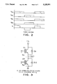
FIG. 1 is a schematic diagram of one embodiment of an electrical converter incorporating the teachings of the present invention;
FIG. 2 is a timing diagram of various waveforms that are present in an electrical converter incorporating the teachings of the present invention;
FIG. 3 is a schematic diagram of one leg of an alternate embodiment of the invention;
FIG. 4 is a schematic diagram of an alternate embodiment of the invention;
FIG. 5 is a schematic diagram of another alternate embodiment of the invention;
FIG. 6 is a schematic diagram of yet another alternate embodiment of the invention;
FIG. 7 is a schematic diagram of still another alternate embodiment of the invention; and
FIG. 8 is a schematic diagram of still another alternate embodiment of the invention.
DETAILED DESCRIPTION OF THE INVENTION
This invention provides a significant reduction in the switching losses in the following manner. All explanations will be based on the half cycle during which Q1 and Q4 conduct. On a typical half cycle, Q1 and Q4 will turn on at the same time, but Q4 will turn off first (refer to FIG. 2). Thus Q2 and Q4 form the leading leg of the bridge and Q1 and Q3 form the trailing leg. When Q4 turns off, capacitors C2 and C4 decrease the rate at which the voltage across Q4 can increase. Thus Q4 turns off at almost zero voltage, and this greatly reduces its turn off loss. This process is called zero voltage switching (ZVS). After Q4 turns off, Q1 continues to conduct and C2 and C4 continue to charge. I0 is almost constant, and as long as Vc4 <V8, I0 continues to flow through the secondary of T1, which also holds I0 almost constant (I0 remains almost constant because of the large value of L0). When Vc4 ≧V8, I0 will flow through D5-D7 and D6-D8 instead of the secondary. I1 will now start to decrease, but Vc4 will continue to charge to a value above V8 because of the energy stored in the leakage inductance, L.sub., and I1 will start to decrease. I1 can now be driven to zero before Q1 turns off, using any one of the three methods described below. This process is called zero current switching (ZCS) because Q1 turns off after I1 =0.
METHOD 1
When Q4 turns off in FIG. 1, all of the energy stored in L1 will be transferred to C2 and C4. This energy is then used by the load on the next half cycle.
This approach minimizes the energy loss, but Vc4 may be so high as to require excessive voltage ratings for Q1-Q4. Naturally, this is especially true for higher values of L1 and/or I1. Note that D2 is used to prevent reverse breakdown of Q2, in which case I1 would circulate in the Q1-Q2 loop, and some of the energy would be dissipated by Q2. If IGBTs with higher reverse breakdown voltages were used, S1, S3, D2 and D4 would be unnecessary as in FIG. 7. However, as shown in FIGS. 1, 4-7, all devices in the Q1 and Q3 legs must be capable of withstanding reverse voltage avalanche. This is because Q1 and Q3 may experience forced commutation under light loading conditions, and controlled avalanche is necessary to limit the resulting voltage transients.
In some cases it is acceptable to allow C2 and C4 to discharge back into V8. If so, Q1, Q3, S1 and S3 are replaced by the circuit in FIG. 3. The advantages of FIG. 3 are the lower collector-emitter voltages of Q1 and Q3 and the absence of the S1, S3 losses. Q1 and Q3 may have higher turn-on losses, however, since the diode recovery current will add to the IGBT turn-on current.
METHOD 2
The preferred configuration for this method is shown in FIG. 4. If Vc4 exceeds V8 plus the breakdown voltage of S2, part of the energy stored in L1 will be transferred to C2 and C4, and the rest will be dissipated by S2 until I1 =0. This approach limits the Q1-Q4 voltage ratings, but the S2 and S4 dissipation may be significant. D2 and D4 prevent Q2 and Q4 breakdown and the associated heating of these devices. If Q2-Q4 breakdown is acceptable, the circuit in FIG. 1 can be used if Schottkys or Zeners are used in place of D2 and D4.
As in Method 1, the replacement circuit in FIG. 3 can be used if C2 and C4 discharge into V8 is acceptable.
METHOD 3
Instead of storing all the energy in C2 and C4 as in method 1 or exceeding the breakdown of S2 as in method 2, Vc4 also can be limited by an active clamp circuit as shown in FIG. 5. Vc4 is limited by the circuitry associated with Q5, while VC2 is limited by the circuitry associated with Q6. Q5-6 can be much smaller than Q1-4. These circuits are similar to the common step-down switching regulator which is controlled by PWM. However, in this case the input voltage, Vc4, is regulated instead of the output, which is connected to V8. Assuming Vc4 >V8, Vc4 monitored by the R1-R2 attenuator and compared to the VR1 reference. If VC4 charges to the desired regulation level, Q5 is activated to transfer the excessive energy to C7, where it can be reused. This circuit avoids the losses associated with the S2 breakdown in FIG. 4, and excessive values of VC4 in FIG. 1. Note the necessity of having Vc4 >V8 in order to drive I to zero after Q4 turn off. Since Vc4 <V8 at smaller loads, D11 is required to keep C5 charged to V8 and prevent excessive Q2 turn on current into C5. Note that C5 >>C4.
As in method 1, S1, S3, D2 and D4 can be avoided as in FIG. 7, if Q1-Q4 have adequate reverse breakdown voltages. The replacement circuit in FIG. 3 can be used if C2 and C4 discharge into V8 is acceptable.
The voltage clamp in FIG. 5 also can be used with the converter in FIG. 8 to provide an active clamp for Q1 and Q3 in addition to Q2 and Q4. This avoids the need for high voltage zener or Schottky diodes without the reverse recovery losses associated with reverse parallel diodes.
On the next half cycle Q2 and Q3 turn on simultaneously. This half cycle then proceeds with Q2 acting in the same manner as Q4 and Q3 acting the same as Q1.
There are also a variety of other ways of achieving ZCS by method 2. In FIG. 6, ZCS is achieved by using breakdown diodes, such as Zeners Z2 and Z4 in parallel with Q2 and Q4. This has the advantage of avoiding the forward voltage drop of S2 and S4, but the diode breakdown voltages must be less than the reverse breakdown voltages of Q2 and Q4.
Another possibility for method 2 is shown in FIG. 7 where ZCS is achieved by simply exceeding the reverse breakdown voltage of Q2 and Q4. This avoids the use of breakdown diodes, but it has the disadvantage of increasing the dissipation in Q2 and Q4. However, this has proven to be effective for some applications. It can only be used with devices such as IGBT's or MCT's that have a large controlled reverse breakdown voltage.
Another important feature is the variable gap between the drive signals for Q2 and Q4 (indicated by dashed lines in FIG. 2). A conventional control system, referred to as phase shift control, has a very small fixed gap between the Q2 and Q4 drive signals. At light load, the variable gap increases and allows additional time to charge C2 and C4 before Q2 turns on. This helps Q2 to avoid the current surge associated with turning on into a partially charged capacitor. This allows the use of larger C2 and C4 values, which further decreases the turn off losses of Q2 and Q4. Since Q1 and Q3 turn off very rapidly, the gap between their drive signals in FIG. 2 can be made extremely small. This increases the conduction time which results in better component utilization. One final advantage is the fact that if Vc4 >V8, as in FIGS. 1, 4, 6 and 7, a slight current flows in the reverse direction through Q1 after its forward current has decreased to zero. This helps to remove any stored charge from Q1. In a conventional circuit, when Q3 turns on to start the next half cycle, a current transient normally flows through Q1 and Q3 due to the remaining store charge Q1. If reverse current is allowed to flow through Q1, this transient is much lower with the ZVS/ZCS converter because of the lower stored charge.
The directional switching flow of current through the primary winding 14 of the transformer 16 acts as an alternating current which will induce a directional switching flow of current through a secondary winding 18 of the transformer 16 at a different voltage than the voltage of the current flow through the primary winding 14. Thus, the voltage in the secondary winding 18 is equal to the voltage in the primary winding 14 multiplied by the ratio of the number of turns in the secondary winding 18 to the number of turns in the primary winding 14, as is understood in the art. The output of the secondary winding 18 of the transformer 16 is rectified to a direct current by a rectifier bridge 20. The rectifier bridge has diodes D5 and D7, with a connection to the secondary winding 18 between the diodes D5 and D7, and it further has diodes D6 and D8, with a second connection to the secondary winding 18 to provide a direct current. This direct current is then filtered by inductor L0 and capacitor C0 before it is applied to the external load R1.
Although the best mode contemplated by the inventor for carrying out the present invention as of the filing date hereof has been shown and described herein, it will be apparent to those skilled in the art that suitable modifications, variations, and equivalence may be made without departing from the scope of the invention, such scope being limited solely by the terms of the following claims.