EP0602495A1 - Resonant-load power supply for arc welding - Google Patents
Resonant-load power supply for arc welding Download PDFInfo
- Publication number
- EP0602495A1 EP0602495A1 EP93119632A EP93119632A EP0602495A1 EP 0602495 A1 EP0602495 A1 EP 0602495A1 EP 93119632 A EP93119632 A EP 93119632A EP 93119632 A EP93119632 A EP 93119632A EP 0602495 A1 EP0602495 A1 EP 0602495A1
- Authority
- EP
- European Patent Office
- Prior art keywords
- power supply
- resonant
- switching
- transformer
- load power
- Prior art date
- Legal status (The legal status is an assumption and is not a legal conclusion. Google has not performed a legal analysis and makes no representation as to the accuracy of the status listed.)
- Granted
Links
Images


Classifications
-
- B—PERFORMING OPERATIONS; TRANSPORTING
- B23—MACHINE TOOLS; METAL-WORKING NOT OTHERWISE PROVIDED FOR
- B23K—SOLDERING OR UNSOLDERING; WELDING; CLADDING OR PLATING BY SOLDERING OR WELDING; CUTTING BY APPLYING HEAT LOCALLY, e.g. FLAME CUTTING; WORKING BY LASER BEAM
- B23K9/00—Arc welding or cutting
- B23K9/10—Other electric circuits therefor; Protective circuits; Remote controls
- B23K9/1006—Power supply
- B23K9/1043—Power supply characterised by the electric circuit
- B23K9/1056—Power supply characterised by the electric circuit by using digital means
-
- H—ELECTRICITY
- H02—GENERATION; CONVERSION OR DISTRIBUTION OF ELECTRIC POWER
- H02M—APPARATUS FOR CONVERSION BETWEEN AC AND AC, BETWEEN AC AND DC, OR BETWEEN DC AND DC, AND FOR USE WITH MAINS OR SIMILAR POWER SUPPLY SYSTEMS; CONVERSION OF DC OR AC INPUT POWER INTO SURGE OUTPUT POWER; CONTROL OR REGULATION THEREOF
- H02M3/00—Conversion of dc power input into dc power output
- H02M3/22—Conversion of dc power input into dc power output with intermediate conversion into ac
- H02M3/24—Conversion of dc power input into dc power output with intermediate conversion into ac by static converters
- H02M3/28—Conversion of dc power input into dc power output with intermediate conversion into ac by static converters using discharge tubes with control electrode or semiconductor devices with control electrode to produce the intermediate ac
- H02M3/325—Conversion of dc power input into dc power output with intermediate conversion into ac by static converters using discharge tubes with control electrode or semiconductor devices with control electrode to produce the intermediate ac using devices of a triode or a transistor type requiring continuous application of a control signal
- H02M3/335—Conversion of dc power input into dc power output with intermediate conversion into ac by static converters using discharge tubes with control electrode or semiconductor devices with control electrode to produce the intermediate ac using devices of a triode or a transistor type requiring continuous application of a control signal using semiconductor devices only
- H02M3/337—Conversion of dc power input into dc power output with intermediate conversion into ac by static converters using discharge tubes with control electrode or semiconductor devices with control electrode to produce the intermediate ac using devices of a triode or a transistor type requiring continuous application of a control signal using semiconductor devices only in push-pull configuration
- H02M3/3376—Conversion of dc power input into dc power output with intermediate conversion into ac by static converters using discharge tubes with control electrode or semiconductor devices with control electrode to produce the intermediate ac using devices of a triode or a transistor type requiring continuous application of a control signal using semiconductor devices only in push-pull configuration with automatic control of output voltage or current
-
- H—ELECTRICITY
- H02—GENERATION; CONVERSION OR DISTRIBUTION OF ELECTRIC POWER
- H02M—APPARATUS FOR CONVERSION BETWEEN AC AND AC, BETWEEN AC AND DC, OR BETWEEN DC AND DC, AND FOR USE WITH MAINS OR SIMILAR POWER SUPPLY SYSTEMS; CONVERSION OF DC OR AC INPUT POWER INTO SURGE OUTPUT POWER; CONTROL OR REGULATION THEREOF
- H02M7/00—Conversion of ac power input into dc power output; Conversion of dc power input into ac power output
- H02M7/42—Conversion of dc power input into ac power output without possibility of reversal
- H02M7/44—Conversion of dc power input into ac power output without possibility of reversal by static converters
- H02M7/48—Conversion of dc power input into ac power output without possibility of reversal by static converters using discharge tubes with control electrode or semiconductor devices with control electrode
- H02M7/53—Conversion of dc power input into ac power output without possibility of reversal by static converters using discharge tubes with control electrode or semiconductor devices with control electrode using devices of a triode or transistor type requiring continuous application of a control signal
- H02M7/537—Conversion of dc power input into ac power output without possibility of reversal by static converters using discharge tubes with control electrode or semiconductor devices with control electrode using devices of a triode or transistor type requiring continuous application of a control signal using semiconductor devices only, e.g. single switched pulse inverters
- H02M7/5387—Conversion of dc power input into ac power output without possibility of reversal by static converters using discharge tubes with control electrode or semiconductor devices with control electrode using devices of a triode or transistor type requiring continuous application of a control signal using semiconductor devices only, e.g. single switched pulse inverters in a bridge configuration
- H02M7/53871—Conversion of dc power input into ac power output without possibility of reversal by static converters using discharge tubes with control electrode or semiconductor devices with control electrode using devices of a triode or transistor type requiring continuous application of a control signal using semiconductor devices only, e.g. single switched pulse inverters in a bridge configuration with automatic control of output voltage or current
- H02M7/53878—Conversion of dc power input into ac power output without possibility of reversal by static converters using discharge tubes with control electrode or semiconductor devices with control electrode using devices of a triode or transistor type requiring continuous application of a control signal using semiconductor devices only, e.g. single switched pulse inverters in a bridge configuration with automatic control of output voltage or current by time shifting switching signals of one diagonal pair of the bridge with respect to the other diagonal pair
-
- H—ELECTRICITY
- H02—GENERATION; CONVERSION OR DISTRIBUTION OF ELECTRIC POWER
- H02M—APPARATUS FOR CONVERSION BETWEEN AC AND AC, BETWEEN AC AND DC, OR BETWEEN DC AND DC, AND FOR USE WITH MAINS OR SIMILAR POWER SUPPLY SYSTEMS; CONVERSION OF DC OR AC INPUT POWER INTO SURGE OUTPUT POWER; CONTROL OR REGULATION THEREOF
- H02M1/00—Details of apparatus for conversion
- H02M1/0083—Converters characterised by their input or output configuration
- H02M1/0085—Partially controlled bridges
-
- Y—GENERAL TAGGING OF NEW TECHNOLOGICAL DEVELOPMENTS; GENERAL TAGGING OF CROSS-SECTIONAL TECHNOLOGIES SPANNING OVER SEVERAL SECTIONS OF THE IPC; TECHNICAL SUBJECTS COVERED BY FORMER USPC CROSS-REFERENCE ART COLLECTIONS [XRACs] AND DIGESTS
- Y02—TECHNOLOGIES OR APPLICATIONS FOR MITIGATION OR ADAPTATION AGAINST CLIMATE CHANGE
- Y02B—CLIMATE CHANGE MITIGATION TECHNOLOGIES RELATED TO BUILDINGS, e.g. HOUSING, HOUSE APPLIANCES OR RELATED END-USER APPLICATIONS
- Y02B70/00—Technologies for an efficient end-user side electric power management and consumption
- Y02B70/10—Technologies improving the efficiency by using switched-mode power supplies [SMPS], i.e. efficient power electronics conversion e.g. power factor correction or reduction of losses in power supplies or efficient standby modes
Definitions
- the present invention relates to a resonant-load power supply for arc welding.
- This arc is powered by appropriate generators capable of delivering even intense currents (50-500A) with voltages on the order of tens of volts (20-45V).
- the power involved can be quite considerable (up to 20 kW), consequently determining the size of the power supply.
- the response speed of the adjustment circuit had the same order of magnitude as the period of the line and was thus often inadequate to the quick variations of the electrical characteristic typical of an electric arc during welding.
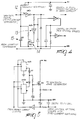
- the configuration of the power stage commonly used in these devices is an asymmetrical half-bridge also known as a "double-transistor forward" half-bridge (figure 2).
- turn-off protection networks which improve overall efficiency and reduce turn-off dissipation of the transistors; furthermore, these networks were indispensable with the semiconductors used in the past.
- the transformer is underutilized with respect to its maximum capacity, which is observed with symmetrical induction.
- the inductance dispersed between the primary and the secondary windings is harmful, since it produces dangerous overvoltages on rectifier diodes, which require very bulky dissipative damping networks.
- the aim of the present invention is to solve the problems linked to the types of power supplies for arc welding machines currently in use.
- a consequent primary object is to provide a power supply which achieves maximum utilization of the power transformer, with a considerable reduction in its bulk.
- a further object is to provide a power supply in which need for dissipation in the transistors-switches is reduced, with a reduction in the dimensions of the heat dissipators.
- a further object is to provide an adjustment system having a better performance than the conventional systems.
- a resonant-load power supply for arc welding characterized in that it comprises:
- the response speed of the adjustment circuit has, in these machines, the same order of magnitude as the period of the line and is thus often inadequate to the rapid variations in electrical characteristics that an electric arc undergoes during welding.
- figure 1 was quickly superseded as soon as switching technology and electronic component technology allowed to develop and perfect switching power supplies powered directly from the line.
- the transformer designated by the reference numeral 2 that adapts the voltage and the current in order to power the arc is therefore much smaller, to the benefit of overall dimensions and weights.
- the configuration of the power stage is an asymmetrical half-bridge, commonly termed "double-transistor forward" configuration, shown in figure 2.
- This is a dual half-wave center-tap rectifier stage constituted by two diodes branched from the center-tap secondary winding of a transformer with high dispersed reactance.
- the circuit is furthermore provided with a fast phase comparator 6 which allows to adjust the operating frequency of the inverter 7 as the load conditions vary.
- FIG 4 illustrates the ultrafast sawtooth signal generator, designated by the reference numeral 11 in figure 3.
- the signal is shown in figure 9, where it is designated by the reference numeral 9d.
- the instant of comparison causes switching in the second power half-bridge and is thus variable with respect to the switching of the other arm, which always coincides with the zero fall of the sawtooth.
- the second protection connectable to the transistors 23 and 24, controls the maximum value of the current.
- This circuitry ensures a very fast adjustment response, preventing saturation of the transformer 3.
- Said gap is in fact designed to increase the magnetizing current to values that are approximately 5-15% of the maximum primary current at the maximum load.
Abstract
Description
- The present invention relates to a resonant-load power supply for arc welding.
- The power supply according to the present invention falls within the technology of electric-arc welding, which as is known is a metal welding process in which the energy required to melt the materials involved originates from an arc powered by electric current.
- This arc is powered by appropriate generators capable of delivering even intense currents (50-500A) with voltages on the order of tens of volts (20-45V).
- Accordingly, the power involved can be quite considerable (up to 20 kW), consequently determining the size of the power supply.
- Very bulky and heavy power supplies which have scarcely satisfactory control dynamics are still in use.
- These devices had an electrical layout of the kind shown in figure 1, substantially constituted by a semi-controlled mains rectifier that required a bulky and heavy line transformer to provide the intended power at a voltage of 25-45 V.
- The response speed of the adjustment circuit had the same order of magnitude as the period of the line and was thus often inadequate to the quick variations of the electrical characteristic typical of an electric arc during welding.
- A later, more modern technology has superseded this type of power supply by means of switching methods and of technologies linked to electronic components that have allowed to develop and perfect switching power supplies supplied directly by the line.
- In these circuits, the line voltage is immediately rectified and smoothed and supplies a solid-state inverter having a rather high switching frequency (20-30 kHz).
- The transformer that adapts the voltage and the current in order to power the electric arc is thus much smaller, to the benefit of total dimensions and weights.
- Furthermore, since the switching period is much shorter (30-50 microseconds), adjustment can be much faster.
- The configuration of the power stage commonly used in these devices is an asymmetrical half-bridge also known as a "double-transistor forward" half-bridge (figure 2).
- This power supply has proved to be interesting, since first of all it is very rugged and allows to handle even very high power levels.
- It also allows to include turn-off protection networks (snubbers), which improve overall efficiency and reduce turn-off dissipation of the transistors; furthermore, these networks were indispensable with the semiconductors used in the past.
- Another advantage was that the output transformer demagnetized itself completely at the end of each operating cycle.
- This meant that subsequent cycles had no "memory" of the preceding cycles, and in principle the subsequent cycles could be very different in terms of duty cycle if this was required by the arc.
- This allowed cycle-by-cycle, and thus intrinsically very fast, adjustment techniques such as the "current-mode" technique, which were otherwise very difficult to achieve.
- Even this circuit, however, had considerable drawbacks.
- It has in fact a configuration which inefficiently uses the magnetic parts, since asymmetrical induction does not allow to utilize the maximum flux change.
- The transformer is underutilized with respect to its maximum capacity, which is observed with symmetrical induction.
- The inductance dispersed between the primary and the secondary windings is harmful, since it produces dangerous overvoltages on rectifier diodes, which require very bulky dissipative damping networks.
- In particular, in order to attempt to obviate this drawback, it is customary to space the two windings, to the benefit of ventilation, but this drastically worsens their coupling and enhances dispersed inductance.
- Furthermore, losses in the switches are not small, since the switchings are forced.
- It is not possible to easily attain high frequencies unless worsening the overall efficiency, with the consequent need to oversize the final stage and the dissipators.
- The aim of the present invention is to solve the problems linked to the types of power supplies for arc welding machines currently in use.
- A consequent primary object is to provide a power supply which achieves maximum utilization of the power transformer, with a considerable reduction in its bulk.
- A further object is to provide a power supply in which need for dissipation in the transistors-switches is reduced, with a reduction in the dimensions of the heat dissipators.
- A further object is to provide an adjustment system having a better performance than the conventional systems.
- With these and other objects in view, there is provided, according to the present invention, a resonant-load power supply for arc welding, characterized in that it comprises:
- a) a dual half-wave center-tap rectifier stage, constituted by two diodes branched from the center-tap secondary winding of a transformer with high dispersed reactance;
- b) a circuit for supplying power to the primary winding of said resonant transformer by virtue of a capacitor, possibly combined with an inductor if the one constituted by the primary winding of the transformer itself is not sufficient;
- c) two pairs of electronic switches, in the power supply circuit, a first pair switching in zero-current conditions and a second pair switching in variable-phase conditions;
- d) driving and control means constituted by a phase comparator that drives a variable-frequency sawtooth oscillator controlling said first pair of switches and, by means of an ultrafast voltage comparator, said second pair of switches as well;
- e) means for controlling the current of the arc and means for protecting the final stage.
- Further characteristics and advantages of the present invention will become apparent from the following detailed description of layouts according to the state of the art and of a preferred embodiment thereof, given by way of non-limitative example and illustrated in the accompanying drawings, wherein:
- figures 1 and 2 are two layouts of power supplies executed according to a known and widespread method;
- figure 3 is a general block diagram of the power supply according to the present invention;
- figure 4 is a more detailed view of part of the layout of figure 3, constituted by an ultrafast sawtooth signal generator;
- figure 5 is a view of another part of the layout of figure 3, constituted by a phase comparator;
- figure 6 is a view of part of the circuit of figure 3, constituted by a primary-current clipper;
- figure 7 is a more detailed view of part of the circuit of figure 3, constituted by a discrete ultrafast voltage comparator;
- figure 7a is a view of an ultrafast integrated comparator that can be combined with the circuit of figure 7;
- figure 8 is a more detailed view of another part of the circuit of figure 3;
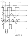
- figure 9 charts a set of typical performance curves of the power supply.
- With reference to the above figures, a known power supply of an electric arc welding machine is built according to the layout of figure 1.
- In this case it is a semi-controlled mains rectifier that requires a bulky and heavy line transformer 1 to provide the 24-45 V required together with the welding current.
- The response speed of the adjustment circuit has, in these machines, the same order of magnitude as the period of the line and is thus often inadequate to the rapid variations in electrical characteristics that an electric arc undergoes during welding.
- The layout of figure 1 was quickly superseded as soon as switching technology and electronic component technology allowed to develop and perfect switching power supplies powered directly from the line.
- In such circuits, like the one shown in figure 2, the line voltage is immediately rectified and smoothed, and supplies a solid-state inverter having a rather high switching frequency (20-30 kHz).
- The transformer, designated by the
reference numeral 2, that adapts the voltage and the current in order to power the arc is therefore much smaller, to the benefit of overall dimensions and weights. - Furthermore, since the switching time is much shorter (30-50 microseconds), adjustment can be considerably faster.
- The configuration of the power stage is an asymmetrical half-bridge, commonly termed "double-transistor forward" configuration, shown in figure 2.
- This configuration uses the magnetic parts inadequately, since induction is asymmetrical and thus it is not possible to utilize the maximum flux variation.
- The transformer is underutilized with respect to its theoretical maximum, which is associated with symmetrical induction.
- The inductance dispersed between the primary and the secondary windings is harmful, since it produces dangerous overvoltages on the rectifier diodes, which require dissipative and bulky damping networks.
- In particular, in welding it is common to space the two windings, in order to improve the ventilation.
- This worsens their coupling and increases dispersed inductance.
- The losses in the switches are not small, since switching is forced.
- It is not possible to easily attain high frequencies, unless worsening the overall efficiency and oversizing the final stage and the dissipators.
- Figure 3 illustrates the power supply according to the invention by means of block diagrams.
- In this configuration, the final stage is constituted by a
transformer 3 and by a pair ofdiodes 4 and 5 that form a so-called "full bridge", whereas the adjustment system, as will become apparent hereinafter, is of the type allowing a so-called "phase variation" between the two half-bridges that form the final stage. - This is a dual half-wave center-tap rectifier stage constituted by two diodes branched from the center-tap secondary winding of a transformer with high dispersed reactance.
- The circuit is furthermore provided with a
fast phase comparator 6 which allows to adjust the operating frequency of theinverter 7 as the load conditions vary. - This allows to optimize the switching time of one of the two pairs of electronic switches, i.e. the pair designated by the
reference numeral 8, reducing dissipation in switching. - For the other pair of switches, designated by the
reference numeral 9, turn-off losses are reduced by pure capacitive snubbers, designated by thereference numeral 10, which can be used due to the resonant nature of the load. - The various components of the layout illustrated in figure 3 reoccur in the subsequent figures.
- Figure 4 illustrates the ultrafast sawtooth signal generator, designated by the reference numeral 11 in figure 3.
- The essential components of this generator are the two
logical gates MOSFET 14 and thetiming capacitor 15. - The signal is shown in figure 9, where it is designated by the reference numeral 9d.
- The zeroing slopes of the sawtooth, designated by the reference numeral 9d1 in figure 9, also cause the switching of the pair of switches designated by the
reference numeral 8 in figure 3, which thus switch at zero current. - The comparator illustrated in figure 5 acts on this generator 11 and corrects the gradient of the ramp of the sawtooth, designated by the reference numeral 9d2 in figure 9, which thus varies the operating frequency.
- The phase comparator compares the rising edges of the control signal of a pair of MOSFETs and of the square wave obtained by clipping the primary current of the
transformer 3, measured with acurrent transformer 16. - In this manner, the phase comparator tends to make the switching of one of the two final half-bridges coincide with the zero value of the primary current, which due to the resonant nature of the load is sinusoidal, as shown in the chart 9c of figure 9, or has a very similar waveform.
- Accordingly, said current naturally becomes zero at every half-cycle.
- In this manner, said pair of output MOSFETs switches at zero or very low current and thus with reduced losses.
- Figure 6 illustrates the primary current clipping circuit formed with an integrated circuit, designated by the
reference numeral 17, and with auxiliary circuits shown in the same figure. - Figures 7 and 7a illustrate the ultrafast voltage comparator, designated by the
reference numeral 18 in the layout of figure 3. - This comparator compares the sawtooth generated by the block shown in figure 4 with the voltage present on the R-C cell formed by the resistor 19 and by the
capacitor 20. - The instant of comparison causes switching in the second power half-bridge and is thus variable with respect to the switching of the other arm, which always coincides with the zero fall of the sawtooth.
- In this manner, by changing the voltage across the R-C cell, the switching time of the second half-bridge changes with respect to the first one, i.e. the phase between the two half-bridges changes.
- The average value per period of the voltage applied to the primary winding of the
transformer 3 changes with it, and thus the power on the load also changes in the required manner. - Figure 7a shows that it is possible to achieve the same result with an ultrafast integrated comparator by inserting the
terminals points - The above mentioned R-C cell is essential for the operation of the power supply.
- The
comparator 21, driven by theswitches 22, thetransistors error amplifier 25 which is part of the block designated by thereference numeral 26 in figure 3, act on said cell, as can be seen in figure 8. - The first two of the above mentioned circuits are protections, and more specifically the first one acts on the average value per cycle of the primary current and is a synchronous integrator having a maximum threshold.
- The second protection, connectable to the
transistors - When these protections, which can operate even for a single half-cycle, intervene, they reduce the voltage across the R-C cell and thus across the comparator, increasing the phase shift between the two MOSFET half-bridges and consequently reducing the power.
- This cell is sized so that it is impossible to have two excessively different successive half-cycles, since it prevents excessively rapid variations of the comparison voltage of the ultrafast discrete comparator.
- This circuitry ensures a very fast adjustment response, preventing saturation of the
transformer 3. - This
transformer 3, which is the output transformer, is constructed so as to enhance its own dispersed reactance. - This reactance of the transformer, which occurs electrically in series to the capacitor 27, resonates with it, possibly in combination with a further reactance, designated by the
reference numeral 28 in figure 3. - The primary and the secondary windings of the
transformer 3 are surrounded by a large air space between them, which certainly improves dissipation of the heat produced during operation. - Said output transformer with wide air spaces, in order to enhance dispersed reactance, is furthermore formed with a gap in the magnetic circuit.
- Said gap, which has an appropriate value, does not only have the conventional purpose of preventing or attenuating possible saturation phenomena, as required in some conventional applications.
- Said gap is in fact designed to increase the magnetizing current to values that are approximately 5-15% of the maximum primary current at the maximum load.
- This effect is not harmful or dissipative, as might be assumed by conventional analysis, but significantly reduces losses of the inverter in no-load or low-load operation.
- In these conditions, in fact, the pair of switches designated by the
reference numeral 9, due to the low current produced by the load, would be forced to dissipate the energy stored by the snubber capacitors arranged in parallel to them. - In non-zero load conditions said switches are in fact already switched on at zero voltage, since the current in the load, which is sinusoidal, discharges the capacitors toward the switch which is about to start conducting.
- In zero-load conditions this would not occur, and the final stages, by switching on, would discharge the energy of said capacitors onto themselves.
- However, if the primary magnetizing current is increased above normal with said gap, the opening of each
switch 9 occurs with such a current as to discharge the capacitors toward the other device, either fully or partially, thus reducing dissipation. - Said electronic switches, designated by the
reference numerals - If the operating frequency is excessively high, it is possible to insert ferrite cores having appropriate dimensions and magnetic characteristics in the air spaces between the primary and the secondary windings of this
transformer 3, said cores having the purpose of increasing the dispersed flux, i.e. the flux which is not concatenated to both windings. - As an alternative, it is possible to eliminate these ferrites, to the benefit of heat dissipation, but in this case it is necessary to add in series to the primary winding a further inductor allowing resonance.
- Considerable advantages are obtained with a configuration of the type described; they can be summarized as follows:
- 1) The dimensions of the magnetic parts are particularly limited, due to the high operating frequency and to the fact that induction is symmetrical.
- 2) Dissipation of the transistors-switches is very low due to the resonance of the system which substantially allows zero switching losses. A consequence of this is a drastic reduction in the metal radiators dissipating heat.
- 3) The dispersed inductance of the transformer is no longer harmful but is indeed desirable, since it becomes part of the resonant-series circuit, fully representing the resonance inductor or constituting a significant part thereof.
- 4) The snubbers on the rectifier diodes are also very small.
- 5) Output filtering is very simple, due to the high switching frequency, which is doubled in output by symmetrical rectification (and is thus approximately equal to 300 kHz). The very cables connecting the machine and the point where the arc forms, generally having an overall lenght not shorter than two meters, contribute to smooth the current with their own, albeit small, inductance.
- 6) Due to the high frequency, the adjustment circuit can be very fast; the adjustment obtained, by virtue of an appropriate calculation of said R-C cell, has a better performance than that obtainable with conventional methods. It is furthermore possible to use the protection circuit on the average primary current, constituted by 21 and 22 of figure 8, or an adequately modified version thereof, to form a so-called "current-mode" control system; the performance obtainable is exceptional in terms of speed of the adjustment, which occurs cycle by cycle, merely by slightly penalizing circuital complexity.
- From what has been described and illustrated it can be seen that the intended aim and objects have all been achieved; the set of circuits shown is only an example, since said circuits can be obtained with different components while maintaining the same operating logic.
- Where technical features mentioned in any claim are followed by reference signs, those reference signs have been included for the sole purpose of increasing the intelligibility of the claims and accordingly such reference signs do not have any limiting effect on the scope of each element identified by way of example by such reference signs.
Claims (8)
- Resonant-load power supply for arc welding, characterized in that it comprises:a) a dual half-wave center-tap rectifier stage, constituted by two diodes (4,5) branched from the center-tap secondary winding of a transformer (3) with high dispersed reactance;b) a circuit (7) for supplying power to the primary winding of said resonant transformer (3) by virtue of a capacitor, possibly combined with an inductor (28) if the one constituted by the primary winding of the transformer itself is not sufficient;c) two pairs of electronic switches, in the power supply circuit, a first pair (8) switching in zero-current conditions and a second pair (9) switching in variable-phase conditions;d) driving and control means constituted by a phase comparator (6) that drives a variable-frequency sawtooth oscillator (11) controlling said first pair (8) of switches and, by means of an ultrafast voltage comparator (18), said second pair (9) of switches as well;e) means (26) for controlling the current of the arc and means for protecting the final stage.
- Resonant-load power supply according to claim 1, characterized in that adjustment is obtained by means of a triangular-wave oscillator (11) the falling edges of which cause the switching of one of the two half-bridges.
- Power supply according to claims 1 and 2, characterized in that the triangular wave obtained with the oscillator according to claim 2 is compared with a variable level by means of an ultrafast voltage comparator (18) of the discrete-transistors or integrated-circuit type, so as to control the second switching time of the second half-bridge.
- Resonant-load power supply according to claim 1, characterized in that it comprises an ultrafast phase comparator (6) which varies the operating frequency of the power supply so as to make the switching of one of the two arms of the power bridge coincide with the zero values of the primary current, thus containing switching losses.
- Resonant-load power supply according to claim 1, characterized in that it has a protection circuit (21,22) on the average primary current, calculated cycle by cycle by means of a synchronous integrator.
- Resonant-load power supply according to claim 1, characterized in that it comprises an R-C cell (19,20) having the purpose, in the case of individual half-cycle intervention of one of the protections, of containing changes in the duration of the successive cycles to avoid saturation of the transformer (3).
- Resonant-load power supply according to claim 1, characterized in that said transformer (3) is formed with widely spaced windings so as to enhance dispersed reactance between the primary and the secondary windings and with a gap in the magnetic circuit, said reactance being suitable to fully or partially constitute the resonance inductance of the output circuit.
- Resonant-load power supply according to claims 1 and 7, characterized in that the air spaces of said transformer (3), formed with wide air spaces between the primary and the secondary windings, are possibly occupied by ferrite cylinders which have the purpose of increasing dispersed reactances and of lowering the switching frequency.
Applications Claiming Priority (2)
| Application Number | Priority Date | Filing Date | Title |
|---|---|---|---|
| ITPD920223A IT1259194B (en) | 1992-12-18 | 1992-12-18 | RESONANT LOAD POWER SUPPLY FOR ARC WELDING |
| ITPD920223 | 1992-12-18 |
Publications (2)
| Publication Number | Publication Date |
|---|---|
| EP0602495A1 true EP0602495A1 (en) | 1994-06-22 |
| EP0602495B1 EP0602495B1 (en) | 1997-05-02 |
Family
ID=11390114
Family Applications (1)
| Application Number | Title | Priority Date | Filing Date |
|---|---|---|---|
| EP93119632A Expired - Lifetime EP0602495B1 (en) | 1992-12-18 | 1993-12-06 | Resonant-load power supply for arc welding |
Country Status (4)
| Country | Link |
|---|---|
| EP (1) | EP0602495B1 (en) |
| DE (1) | DE69310328T2 (en) |
| DK (1) | DK0602495T3 (en) |
| IT (1) | IT1259194B (en) |
Cited By (9)
| Publication number | Priority date | Publication date | Assignee | Title |
|---|---|---|---|---|
| GB2300079A (en) * | 1995-04-20 | 1996-10-23 | Bettermann Obo Gmbh & Co Kg | Circuitry of a charging circuit for a welding capacitor |
| EP0777931A1 (en) * | 1995-06-01 | 1997-06-11 | Allan A. Nostwick | Phase controlled bridge |
| WO2001003874A1 (en) * | 1999-07-13 | 2001-01-18 | Selco S.R.L. | Generator for arc welding machines |
| WO2001053030A1 (en) * | 2000-01-20 | 2001-07-26 | Fronius International Gmbh | Method for regulating and/or controlling a welding current source with a resonance circuit |
| WO2004071703A1 (en) * | 2003-02-14 | 2004-08-26 | Selco S.R.L. | Generator for arc welder with high power factor |
| EP1564874A1 (en) * | 2004-02-12 | 2005-08-17 | La Soudure Autogene Francaise | Arc welding unit with power source and inverter |
| EP1564876A1 (en) | 2004-02-12 | 2005-08-17 | La Soudure Autogene Francaise | Welding unit with soft switching quasi-resonant inverter |
| CN109262125A (en) * | 2018-09-25 | 2019-01-25 | 常州铭赛机器人科技股份有限公司 | Transistor type resistance welder electric power system and its control method |
| CN113809943A (en) * | 2021-09-30 | 2021-12-17 | 华南理工大学 | LLC digital welding power supply system based on bridgeless PFC and control method |
Families Citing this family (2)
| Publication number | Priority date | Publication date | Assignee | Title |
|---|---|---|---|---|
| CN101367151B (en) * | 2008-09-16 | 2011-02-16 | 李明杰 | Circuit for reducing wire distribution control cable component wire of gas shielded welding machine |
| DE102012023425A1 (en) * | 2012-11-29 | 2014-06-05 | Leopold Kostal Gmbh & Co. Kg | Voltage transformer for DC |
Citations (3)
| Publication number | Priority date | Publication date | Assignee | Title |
|---|---|---|---|---|
| GB2019135A (en) * | 1978-04-12 | 1979-10-24 | Migatronic Svejsemask | Direct current arc welding apparatus |
| FR2547128A1 (en) * | 1983-06-03 | 1984-12-07 | Nat Semiconductor Corp | REGULATED SWITCHED POWER SUPPLY CIRCUIT HAVING RESONANT LOAD |
| EP0345981A2 (en) * | 1988-06-09 | 1989-12-13 | Powcon Incorporated | System for supplying power |
-
1992
- 1992-12-18 IT ITPD920223A patent/IT1259194B/en active IP Right Grant
-
1993
- 1993-12-06 DE DE69310328T patent/DE69310328T2/en not_active Expired - Lifetime
- 1993-12-06 EP EP93119632A patent/EP0602495B1/en not_active Expired - Lifetime
- 1993-12-06 DK DK93119632.3T patent/DK0602495T3/en active
Patent Citations (3)
| Publication number | Priority date | Publication date | Assignee | Title |
|---|---|---|---|---|
| GB2019135A (en) * | 1978-04-12 | 1979-10-24 | Migatronic Svejsemask | Direct current arc welding apparatus |
| FR2547128A1 (en) * | 1983-06-03 | 1984-12-07 | Nat Semiconductor Corp | REGULATED SWITCHED POWER SUPPLY CIRCUIT HAVING RESONANT LOAD |
| EP0345981A2 (en) * | 1988-06-09 | 1989-12-13 | Powcon Incorporated | System for supplying power |
Cited By (20)
| Publication number | Priority date | Publication date | Assignee | Title |
|---|---|---|---|---|
| GB2300079A (en) * | 1995-04-20 | 1996-10-23 | Bettermann Obo Gmbh & Co Kg | Circuitry of a charging circuit for a welding capacitor |
| GB2300079B (en) * | 1995-04-20 | 1999-06-30 | Bettermann Obo Gmbh & Co Kg | Circuitry of a charging circuit for a welding capacitor |
| EP0777931A1 (en) * | 1995-06-01 | 1997-06-11 | Allan A. Nostwick | Phase controlled bridge |
| EP0777931A4 (en) * | 1995-06-01 | 1999-06-02 | Allan A Nostwick | Phase controlled bridge |
| WO2001003874A1 (en) * | 1999-07-13 | 2001-01-18 | Selco S.R.L. | Generator for arc welding machines |
| CZ301980B6 (en) * | 1999-07-13 | 2010-08-25 | Selco S. R. L. | Generator for arc welding machines |
| US6570128B1 (en) | 1999-07-13 | 2003-05-27 | Selco S.R.L. | Generator for arc welding machines |
| AU770162B2 (en) * | 1999-07-13 | 2004-02-12 | Selco S.R.L. | Generator for arc welding machines |
| AT412388B (en) * | 2000-01-20 | 2005-02-25 | Fronius Schweissmasch Prod | METHOD FOR REGULATING A WELDING CURRENT SOURCE WITH A RESONANCE CIRCUIT |
| US6849828B2 (en) | 2000-01-20 | 2005-02-01 | Fronius International Gmbh | Method for regulating and/or controlling a welding current source with a resonance circuit |
| WO2001053030A1 (en) * | 2000-01-20 | 2001-07-26 | Fronius International Gmbh | Method for regulating and/or controlling a welding current source with a resonance circuit |
| WO2004071703A1 (en) * | 2003-02-14 | 2004-08-26 | Selco S.R.L. | Generator for arc welder with high power factor |
| US7576299B2 (en) | 2003-02-14 | 2009-08-18 | Selco S.R.L. | Generator for arc welder with high power factor |
| NO338243B1 (en) * | 2003-02-14 | 2016-08-08 | Selco Srl | Generator for high power factor welding. |
| EP1564874A1 (en) * | 2004-02-12 | 2005-08-17 | La Soudure Autogene Francaise | Arc welding unit with power source and inverter |
| EP1564876A1 (en) | 2004-02-12 | 2005-08-17 | La Soudure Autogene Francaise | Welding unit with soft switching quasi-resonant inverter |
| CN109262125A (en) * | 2018-09-25 | 2019-01-25 | 常州铭赛机器人科技股份有限公司 | Transistor type resistance welder electric power system and its control method |
| CN109262125B (en) * | 2018-09-25 | 2021-08-24 | 常州铭赛机器人科技股份有限公司 | Transistor type resistance welding power supply system and control method thereof |
| CN113809943A (en) * | 2021-09-30 | 2021-12-17 | 华南理工大学 | LLC digital welding power supply system based on bridgeless PFC and control method |
| CN113809943B (en) * | 2021-09-30 | 2024-02-06 | 华南理工大学 | LLC digital welding power supply system based on bridgeless PFC and control method |
Also Published As
| Publication number | Publication date |
|---|---|
| IT1259194B (en) | 1996-03-11 |
| EP0602495B1 (en) | 1997-05-02 |
| DK0602495T3 (en) | 1997-11-03 |
| DE69310328T2 (en) | 1997-08-14 |
| ITPD920223A0 (en) | 1992-12-18 |
| ITPD920223A1 (en) | 1994-06-18 |
| DE69310328D1 (en) | 1997-06-05 |
Similar Documents
| Publication | Publication Date | Title |
|---|---|---|
| US5796598A (en) | Voltage-converting circuit for the power supply of an electrical consumer of high output, particularly a bobbin winding machine | |
| EP0614267B1 (en) | Lossless active snubber for half-bridge output rectifiers | |
| US5796595A (en) | Interleaved continuous flyback power converter system | |
| US4864479A (en) | Full-bridge lossless switching converter | |
| US6031737A (en) | AC-DC power supply | |
| US5471376A (en) | Low-loss active voltage-clamp circuit for single-ended forward PWM converter | |
| US4933831A (en) | Power supply | |
| US6021053A (en) | Method and apparatus for switching circuit system including a saturable core device with multiple advantages | |
| Ramanarayanan et al. | Course material on switched mode power conversion | |
| EP0602495B1 (en) | Resonant-load power supply for arc welding | |
| EP0698961A2 (en) | Low-loss clamp circuit | |
| WO1999022436A1 (en) | Ac to dc conversion arrangement | |
| US7576299B2 (en) | Generator for arc welder with high power factor | |
| WO1991010280A1 (en) | A power inverter snubber circuit | |
| JP2002233150A (en) | Resonance-type dc-to-dc converter | |
| US5229930A (en) | Welding inverter and method for controlling a welding inverter | |
| JPH08228486A (en) | Control method of dc-ac inverter | |
| JP2982364B2 (en) | Inverter for induction heating | |
| JP3493273B2 (en) | Power factor improvement circuit of three-phase rectifier | |
| Trabach et al. | A stabilized single phase electronic autotransformer | |
| Chen et al. | Design and implementation of a passively clamped quasi resonant DC link inverter | |
| JPH07284271A (en) | Switching power supply apparatus | |
| JP2002051564A (en) | Snubber circuit | |
| JP3511912B2 (en) | High frequency heating equipment | |
| KR20010039221A (en) | Zero voltage and zero current switching full bridge dc-dc converter |
Legal Events
| Date | Code | Title | Description |
|---|---|---|---|
| PUAI | Public reference made under article 153(3) epc to a published international application that has entered the european phase |
Free format text: ORIGINAL CODE: 0009012 |
|
| AK | Designated contracting states |
Kind code of ref document: A1 Designated state(s): BE CH DE DK FR GB LI NL SE |
|
| 17P | Request for examination filed |
Effective date: 19941129 |
|
| GRAG | Despatch of communication of intention to grant |
Free format text: ORIGINAL CODE: EPIDOS AGRA |
|
| 17Q | First examination report despatched |
Effective date: 19960619 |
|
| GRAH | Despatch of communication of intention to grant a patent |
Free format text: ORIGINAL CODE: EPIDOS IGRA |
|
| GRAH | Despatch of communication of intention to grant a patent |
Free format text: ORIGINAL CODE: EPIDOS IGRA |
|
| GRAA | (expected) grant |
Free format text: ORIGINAL CODE: 0009210 |
|
| AK | Designated contracting states |
Kind code of ref document: B1 Designated state(s): BE CH DE DK FR GB LI NL SE |
|
| REG | Reference to a national code |
Ref country code: CH Ref legal event code: NV Representative=s name: BUECHEL & PARTNER AG PATENTBUERO Ref country code: CH Ref legal event code: EP |
|
| REF | Corresponds to: |
Ref document number: 69310328 Country of ref document: DE Date of ref document: 19970605 |
|
| ET | Fr: translation filed | ||
| REG | Reference to a national code |
Ref country code: DK Ref legal event code: T3 |
|
| PLBE | No opposition filed within time limit |
Free format text: ORIGINAL CODE: 0009261 |
|
| STAA | Information on the status of an ep patent application or granted ep patent |
Free format text: STATUS: NO OPPOSITION FILED WITHIN TIME LIMIT |
|
| 26N | No opposition filed | ||
| REG | Reference to a national code |
Ref country code: GB Ref legal event code: IF02 |
|
| PGFP | Annual fee paid to national office [announced via postgrant information from national office to epo] |
Ref country code: FR Payment date: 20101213 Year of fee payment: 18 Ref country code: DK Payment date: 20101130 Year of fee payment: 18 |
|
| PGFP | Annual fee paid to national office [announced via postgrant information from national office to epo] |
Ref country code: CH Payment date: 20101129 Year of fee payment: 18 |
|
| PGFP | Annual fee paid to national office [announced via postgrant information from national office to epo] |
Ref country code: GB Payment date: 20101217 Year of fee payment: 18 Ref country code: SE Payment date: 20101221 Year of fee payment: 18 Ref country code: NL Payment date: 20101231 Year of fee payment: 18 |
|
| PGFP | Annual fee paid to national office [announced via postgrant information from national office to epo] |
Ref country code: DE Payment date: 20101222 Year of fee payment: 18 |
|
| PGFP | Annual fee paid to national office [announced via postgrant information from national office to epo] |
Ref country code: BE Payment date: 20101202 Year of fee payment: 18 |
|
| BERE | Be: lapsed |
Owner name: *SELCO S.R.L. Effective date: 20111231 |
|
| REG | Reference to a national code |
Ref country code: NL Ref legal event code: V1 Effective date: 20120701 |
|
| REG | Reference to a national code |
Ref country code: DK Ref legal event code: EBP |
|
| REG | Reference to a national code |
Ref country code: CH Ref legal event code: PL Ref country code: SE Ref legal event code: EUG |
|
| GBPC | Gb: european patent ceased through non-payment of renewal fee |
Effective date: 20111206 |
|
| REG | Reference to a national code |
Ref country code: FR Ref legal event code: ST Effective date: 20120831 |
|
| REG | Reference to a national code |
Ref country code: DE Ref legal event code: R119 Ref document number: 69310328 Country of ref document: DE Effective date: 20120703 |
|
| PG25 | Lapsed in a contracting state [announced via postgrant information from national office to epo] |
Ref country code: CH Free format text: LAPSE BECAUSE OF NON-PAYMENT OF DUE FEES Effective date: 20111231 Ref country code: LI Free format text: LAPSE BECAUSE OF NON-PAYMENT OF DUE FEES Effective date: 20111231 Ref country code: BE Free format text: LAPSE BECAUSE OF NON-PAYMENT OF DUE FEES Effective date: 20111231 Ref country code: SE Free format text: LAPSE BECAUSE OF NON-PAYMENT OF DUE FEES Effective date: 20111207 Ref country code: DE Free format text: LAPSE BECAUSE OF NON-PAYMENT OF DUE FEES Effective date: 20120703 Ref country code: GB Free format text: LAPSE BECAUSE OF NON-PAYMENT OF DUE FEES Effective date: 20111206 |
|
| PG25 | Lapsed in a contracting state [announced via postgrant information from national office to epo] |
Ref country code: DK Free format text: LAPSE BECAUSE OF NON-PAYMENT OF DUE FEES Effective date: 20120102 Ref country code: NL Free format text: LAPSE BECAUSE OF NON-PAYMENT OF DUE FEES Effective date: 20120701 |
|
| PG25 | Lapsed in a contracting state [announced via postgrant information from national office to epo] |
Ref country code: FR Free format text: LAPSE BECAUSE OF NON-PAYMENT OF DUE FEES Effective date: 20120102 |