US5174159A - Linear displacement and strain measuring apparatus - Google Patents
Linear displacement and strain measuring apparatus Download PDFInfo
- Publication number
- US5174159A US5174159A US07/722,487 US72248791A US5174159A US 5174159 A US5174159 A US 5174159A US 72248791 A US72248791 A US 72248791A US 5174159 A US5174159 A US 5174159A
- Authority
- US
- United States
- Prior art keywords
- emitter
- plate
- detector
- disposed
- conductive
- Prior art date
- Legal status (The legal status is an assumption and is not a legal conclusion. Google has not performed a legal analysis and makes no representation as to the accuracy of the status listed.)
- Expired - Lifetime
Links
Images


Classifications
-
- G—PHYSICS
- G01—MEASURING; TESTING
- G01B—MEASURING LENGTH, THICKNESS OR SIMILAR LINEAR DIMENSIONS; MEASURING ANGLES; MEASURING AREAS; MEASURING IRREGULARITIES OF SURFACES OR CONTOURS
- G01B7/00—Measuring arrangements characterised by the use of electric or magnetic techniques
- G01B7/16—Measuring arrangements characterised by the use of electric or magnetic techniques for measuring the deformation in a solid, e.g. by resistance strain gauge
Definitions
- This invention relates in general to apparatus for sensing relative displacement, and in particular instances to apparatus for measuring strain in an object.
- Measurement of strain (the change in length of an object in some direction per unit undistorted length) in specimens and objects may be carried out either directly or indirectly.
- Some of the approaches used for direct strain measurements include the use of bonded wire strain gauges (in which a grid of strain sensitive wire is cemented to a specimen so that a change in the length of the grid due to strains in that specimen changes the resistance of the wire which can then be measured), mechanical strain gauges (in which optical or mechanical lever systems are employed to multiply the strain which may then be read from a suitable scale), magnetic strain gauges (which include magnetic circuits having air gaps which, when varied as a result of a strain in the specimens, varies the permeance of the circuits to provide an indication of the strains produced), semiconductor strain gauges (in which the resistance of a piezoelectric material varies with applied stress and resulting strain in the material), capacitance strain gauges (in which a variation of capacitance caused by variation in the separation of elements due to strain in the specimen, can be measured to provide a reading of the strain
- Approaches for indirectly measuring strain in a specimen include the use of displacement pick-up devices, velocity pick-up devices, and acceleration detection devices.
- a disadvantage of some of the conventional approaches to measuring strain is that the devices employed are oftentimes difficult to attach to or use with a specimen whose strain is to be measured. Also, such devices are typically difficult and costly to manufacture. Finally, because of the intrinsically high axial rigidity of many of such devices, it requires high quality bonding of the devices to the specimen to prevent detachment due to failure of the bond and this, in turn, requires time-consuming and careful preparation of the specimen for bonding.
- VLSI very large scale integration
- a linear displacement and strain measuring device which includes a linearly moveable element whose linear displacement is to be measured, an emitter disposed on the moveable element to move as the element is moved, for developing predetermined patterns of electric fields which vary linearly on the emitter in the direction of movement of the element, and a detector disposed in close proximity to the emitter adjacent the path in which the emitter moves to detect variation in the electric field patterns as the emitter is moved, for producing output signals representing variations in the electric field patterns.
- Such variations provide an indication of the position and displacement of the emitter relative to the detector.
- the emitter comprises a generally planar emitter plate mounted on the linearly moveable element to move in the plane defined by the emitter plate and to direct the electric fields normally from an active side of the plate.
- the detector includes a generally planar detector plate disposed in a fixed position generally parallel with the emitter plate on the active side thereof to thereby detect variation in the electric field patterns as the emitter plate is moved.
- the moveable element comprises an elongate tab which may be attached to the object in which strain is to be measured.
- the emitter plate is mounted on the tab and includes a plurality of emitter element sections formed in predetermined patterns on the active side of the plate to develop electric fields in response to electric input signals.
- the device further includes an electric signal generator for supplying electric input signals to the emitter element sections.
- a plurality of linear tracks are formed on the active side of the emitter plate, with each track including a plurality of spaced-apart conductive sections.
- a conductive layer of material is disposed on the detector plate on the side facing the active side of the emitter plate for developing an electric field to capacitively couple the layer and the track sections when a voltage signal is supplied to the layer.
- the conductive sections are thus caused to develop electric fields to be detected by the detector.
- a voltage supply source supplies the voltage signal to the conductive layer of the material on the detector plate.
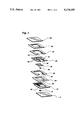
- FIG. 1 is an exploded view of a linear displacement and strain measuring device made in accordance with the principles of the present invention
- FIG. 2 is a top, plan view of the H-structure, normal force spring, and emitter of FIG. 1;
- FIG. 3 are top, plan views of the detector and emitter of the device of FIG. 1;
- FIG. 3A is a top, plan view of another embodiment of an emitter for use in the present invention.
- FIG. 4 is a top, plan, graphic representation of one embodiment of the emitter of the present invention, shown to include Gray code tracks and a Vernier array;
- FIG. 5 is a top, schematic view showing sensing elements positioned relative to linear tracks of one emitter embodiment of the present invention
- FIG. 6 is a schematic of one embodiment of an analog-to-digital converter suitable for use in the present invention.
- FIG. 7 is a schematic and diagrammatic representation of linear complementary tracks presenting a Gray code configuration
- FIG. 8 is a graph plotting of representative outputs of Vernier array sensors of the present invention.
- FIG. 1 there is shown an exploded view of one specific illustrative embodiment of a linear displacement and strain measuring transducer made in accordance with the present invention for measuring strain in a specimen to which the transducer is attached.
- the transducer includes a base plate 4 which would be attached to a specimen in which strain was to be measured.
- a detector plate 8 is disposed on the base plate 4 in a fixed position.
- a spacer 12, formed with an opening 16, is disposed on the base plate 4 to circumscribe the detector 8, and a flex circuit board 20 is mounted on the base plate 4 within the opening 16 of the spacer 12.
- the flex circuit board 20 is made of a flexible material such as plastic and carries electrical conductors for connecting to the detector plate 8 to supply signals thereto and carry signals therefrom.
- Another spacer 24 is disposed on the spacer 12, and still a third spacer 28 is disposed on the spacer 24.
- An opening 32 is formed in one side of the spacer 28 to accommodate an elastomer seal for surrounding a tab 36 of an H-shaped support plate or structure 40, as will be discussed momentarily.
- the H-structure 40 is a flexible plate which includes a frame 44 and the elongate tab 36 coupled to the frame by way of legs 48 to allow movement of the tab relative to the frame.
- Attached to the underside of the tab 36 is a normal force spring 34, and mounted on the normal force spring centrally thereof is an emitter plate or chip 38.
- the emitter 38 projects through the central openings in the spacers 28 and 24 to lightly contact the detector plate 8.
- the thickness of the spacers 28 and 24 are selected to allow the emitter chip 38 to just contact the detector plate 8.
- a spacer 52 Mounted on the H-structure 40 is a spacer 52 having an opening 56 in one side thereof, again to accommodate the elastomer seal for the tab 36.
- Another spacer 60 is disposed on top of the spacer 52 and a cover plate 64 is disposed on the spacer 60 to cover the assembly package and prevent contamination of the parts thereof.
- openings 32 and 56 of the spacers 28 and 52 respectively are formed to allow projection therethrough of the tab 36.
- a flexible elastomer seal (not shown) would fill the openings 32 and 56 to seal about the tab 36 to allow movement of the tab but also prevent entry into the package of contaminants, etc.
- the base plate 4 and cover plate 64 might illustratively be made of metal such as beryllium copper, the spacers 12, 24, 28, 52 and 60 might also be made of a metal such as beryllium copper.
- the H-structure 40 is made of a resilient metal, as is the normal force spring 34. The parts would be joined together using conventional bonding techniques.
- FIG. 2 shows a top, plan view of the H-structure 40 of FIG. 1 to include a plate frame 44 to which an elongate tab 36 is coupled.
- the tab 36 would be attached at its free end to a specimen in which the strain was to be measured, and, as already indicated, the base plate 4 (FIG. 1) would also be attached to the specimen so that strain occurring in the specimen at the location of attachment of the base plate and tab would cause movement of the tab relative to the base plate and thus relative to the frame 44.
- the frame 44 includes a pair of side rails 100 and 104 joined at one of their ends by an end rail 108.
- the other ends of the side rails 100 and 104 are formed with large plate sections 112 and 116 respectively.
- the tab 36 extends between the plate sections 112 and 116 and terminates in an enlarged mounting section 120.
- the mounting section 120 is coupled at one side by a pair of legs 124 and 128 to the side rail 100, and at the other side by a pair of legs 132 and 136 to the side rail 104.
- the frame 44 is made of a resilient material such as beryllium copper to allow flexing of the legs 124, 128, 132 and 136 and thus movement of the elongate tab 36 linearly relative to the frame.
- tabs 140 and 144 Extending laterally from either side of the enlarged mounting section 120 are tabs 140 and 144 on which a normal force spring plate 34 is mounted.
- the plate sections 112 and 116 also include tabs 148 and 152 which extend toward one another and into cutout sections 156 and 160 respectively of the elongated tab 36.
- the tabs 148 and 152 serve as stops to limit linear excursion of the tab 36 and prevent movement in either direction beyond a certain point. That is, the tabs 148 and 152 contact the edges of the cutout sections 156 and 160 to prevent further movement of the tab beyond certain limits.
- the normal force spring plate 34 includes a central section 164 onto which the emitter chip 38 is mounted.
- the normal force spring plate 34 also includes a border region 168 which circumscribes the central section 164 and is joined thereto by a plurality of legs 172.
- the normal force spring plate 34 is made of a resilient material to bias or urge the central section 164, and thus the emitter chip 38, normally outwardly away from the enlarged mounting section 120 of the H-structure 40.
- the normal force spring plate 34 is mounted onto the tabs 140 and 144 by means of mounting feet, shown by dotted line 176, which hold the normal force spring plate above the enlarged mounting section 120.
- the combination of the resiliency of the normal force spring plate 34 and the location of the mounting feet 176 serve to bias or urge the emitter 38 normally outwardly from the H-structure 40 and towards the detector 8 (FIG. 1) as described earlier.
- the emitter could be held by a mechanical support just out of contact with the detector.
- FIG. 3 shows top, plan, diagrammatic views of the detector plate 8 and the emitter chip 38 of FIG. 1.
- the parts of the emitter chip 38 would be positioned on the bottom side of the chip and then the chip would be disposed over the detector chip 8 as earlier described.
- the emitter chip 38 is disposed to move linearly in the direction indicated by arrows 202.
- the chip 38 comprises a sapphire plate 203 on which are formed a plurality of linear tracks 204 positioned side-by-side to extend generally parallel with the direction of movement of the chip.
- Each of the tracks 204 is formed with alternating conductive and nonconductive segments, the conductive segments 208 being shown as shaded and the nonconductive segments being shown as unshaded.
- the track representations 204 are drawn simple to illustrate the idea of segmentation and should not be taken to represent an actual pattern such as that shown in FIG. 7.
- the conductive segments 208 are electrically coupled together and to a conductive sheet 224 which overlays a large portion of the plate 203.
- the conductive segments 208 and conductive layer 224 could be made, for example, of a layer or film of aluminum. As will be discussed, the conductive segments 208 may be energized to produce an electric field pattern which varies linearly over the tracks 204. Because the conductive segments 208 are all electrically connected together, the conductive pattern is electrically continuous with no isolated regions to enable electrifying the pattern by capacitive coupling as will also be described later.
- the conductive pattern of sections on the emitter chip 38 is formed to present a Gray code such that movement of the emitter chip past a transverse locus of points (at which electric field sensors will be located) results in incremental changes in the value of the code.
- this value may be detected to provide an indication of the linear displacement of the emitter relative to the detector, and thus an indication of strain.
- FIG. 4 A graphic representation of the tracks 204 is shown in FIG. 4.
- the tracks are formed as complementary or conjugate pairs 252, 256, etc., as indicated, except that each track of a pair is spaced at least one track apart from the other track of the pair, as shown in FIG. 7.
- the tracks of each pair are shown positioned side-by-side in FIG. 4 simply for ease of explanation.
- the complementary or conjugate aspect of each pair of tracks is illustrated by reference to segments 252a and 252b of the pair of tracks 252.
- Segment 252a is shown as shaded in FIG. 4 indicating that it is metallized or is formed of a conductive layer of material, whereas the light or unshaded segment 252b indicates that the segment is nonconductive.
- Segments 252a and 252b occupy the same transverse position on the emitter plate, but, of course, in separate, spaced-apart tracks.
- segments 256a and 256b (being larger than segments 252a and 252b) are conjugate in that section 256a is metallized and 256b is unmetallized.
- the metallized segments are capable of producing an electric field whereas the unmetallized segments are not, and in this manner an electric field is developed on the emitter chip which varies linearly in the direction of movement of the chip.
- an array 212 of conductive fingers 216 positioned side-by-side transversely of the array axis.
- the conductive fingers 216 are all coupled by a conductor 220 to the conductive sheet 224 so that energizing the conductive sheet will result in energizing the conductive fingers to produce electric fields just as do the metallized segments 208.
- the conductive finger array 212 is formed into a Vernier array to provide a means of determining position and movement of the emitter chip 38 between increments or transitions from one value to the next of the Gray code tracks 204. That is, transitions from one value to another value along the Gray code tracks 204 occur over a certain interval or distance of movement, and the Vernier array 212 is provided to determine positions and movement within such interval. Vernier measurement of linear displacement was described in U.S. Pat. No. 4,964,306, which is incorporated herein by reference, and the same techniques are utilized here.
- the Gray code tracks 204 thus provide a large dynamic range for the transducer of the present invention, and the Vernier array 212 provides desired high resolution.
- the detector plate 8 shown in FIG. 3 and made for example of silicon, includes an array of electric field sensors 232 positioned to extend transversely of the segmented tracks 204 when the emitter chip 38 is disposed over the detector plate 8. As will be described in detail later, each sensor in the array 232 is disposed opposite a respective one of the segmented tracks. Also formed on the detector plate 8 is a second array of electric field sensors 236 positioned to lie opposite the conductive finger array 212 when the emitter plate 38 and detector plate 8 are assembled as indicated in FIG. 1.
- the sensors of the array 236 are best shown in FIG. 4 as transverse detector elements 260 which are uniformly spaced just slightly farther apart than are the uniformly spaced underlying conductive fingers 212. That is, over a given distance of the sensor array 236 and conductive finger array 212 there will be one more conductive fingers than sensors and this configuration defines the Vernier measuring scales of the transducer.
- FIG. 7 shows an exemplary arrangement complimentary tracks laid out in an linear array and formed to present a Gray code.
- the tracks are shown to the right, with the metalized portions being shaded to represent "0's", and a nonmetalized portion representing "1's".
- the corresponding code value for each incremental advance along the tracks is shown to the left, and, as can be seen, the code value increases by one bit while advancing incrementally from the top to the bottom of the tracks.
- all metalized portions of the track are electrically continuous and can be readily fabricated using etching and photolitographic techniques.
- a conductive sheet 240 disposed to cover about two-thirds of the detector plate 8 to partially surround the sensor array 232.
- An integrated circuit 228 is also formed on the detector plate 8 to provide the processing logic for calculating linear displacement or strain detected by the sensor arrays 232 and 236 of the emitter plate 38.
- the integrated circuit 228 also provides energizing signals to the conductive sheet 240 in the form of square wave signals.
- the conductive sheet 240 develops electric fields which capacitively couple the conductive sheet 240 with the conductive sheet 224 of the emitter chip 38; the conductive segments 208 and conductive fingers 212 are thereby energized to produce the desired electric field patterns.
- FIG. 3A shows a top, plan view of an alternative embodiment of the emitter of the present invention.
- two sets 241 and 242 of interdigitated conductive fingers are provided, each set being electrically coupled to a respective conductive sheets 243 and 244.
- Two separate conductive sheets on the corresponding detector plate would capacitively couple the conductive sheets 243 and 244 to drive or energize the conductive finger arrays 241 and 242 180 degrees out of phase to provide a bipolar emitter array.
- the advantage of the bipolar emitter array is that better contrast in the electric field emitted by the interdigitated fingers is achieved and this enhances the resolution of the transducer.
- FIG. 5 there is shown a schematic view of a portion of an emitter chip 304 showing a plurality of segmented tracks 308. Shown disposed over the tracks in two arrays are a transverse array of sensors 312 (Gray code array) and a colinear array of sensors 316 (Vernier array).
- the Vernier array 316 rather than being made up of conductive fingers as discussed for FIGS. 3, 3A and 4, alternatively is composed of a pair of complimentary, segmented tracks 318.
- Each sensor in the arrays includes two electric field sensing elements, such as elements 320 and 324, each disposed over a respective track of a complimentary pair for intercepting electric fields emanating from the tracks.
- Each sensor in the arrays also includes a regenerative differential amplifier, such as amplifier 328, coupled to the sensing elements (such as sensing elements 320 and 324).
- amplifier 328 coupled to the sensing elements (such as sensing elements 320 and 324).
- opposite signals for example, a high and a low signal
- the differential amplifier 328 produces an output signal representing the difference between values of the input signals.
- the regenerative differential amplifier contains circuitry such that when it is strobed, it will give a first signal if the amount of coupled field on the first of its two sensor plates is greater than that on its second plate, and it gives a second signal if the second plate has received the greater coupled electric field.
- the number of sensors is one less than the number of segment transitions (or conductive fingers, if fingers are used) over the portion of the tracks 318 covered by the Vernier array.
- very small linear displacements of the emitter chip 304 will cause successive ones of the sensors in the Vernier array 316 to detect transitions to thereby provide readings or measurements of small incremental displacements.
- the Vernier array 316 provides fine readings of linear displacement between successive increments or changes in Gray code value, as detected by the transverse array of sensors 312.
- the sensors including the sensing elements and differential amplifiers, are fabricated on the detector plate utilizing VLSI manufacturing techniques.
- the outputs of the sensors are supplied to interpretation and computational logic which is also fabricated on the detector plate (identified as integrated circuit 228 in FIG. 3) using VLSI techniques.
- Such logic includes Vernier array interpretation logic 330 which receives the output from the sensors in the Vernier array of sensors 316 and converts the Vernier scale readout, represented by the sensor output, into a binary coded value. This can be done by table look-up, conventional combinatorial logic, or statistical sampling. This binary value is supplied by the logic 330 to a combining logic circuit 333. Circuit 333 combines information from the Vernier and Gray code arrays into a final output digital value indicating displacement.
- the outputs from the sensors in the Gray code sensor array 312 are supplied to a Gray code to binary converter 332 which converts the sensor outputs to a binary representation of the value of the Gray code encountered by the Gray code sensor array.
- This binary information is supplied to the combining logic circuit 333 which combines the information with the binary information received from the logic 330 and supplies it to a shift register 334.
- the binary information stored in the shift register 334 provides an indication of linear position or displacement of the emitter chip 304 and thus an indication of strain occurring in the specimen on which the transducer is mounted.
- the information stored in the shift register 334 may be selectively shifted from the register to a bus transceiver 338 in response to a shift signal received from a counter/comparator circuit 340.
- the counter/comparator circuit 340 counts clock pulses supplied by the bus transceiver 338 and when the count reaches a value corresponding to an address stored in an address register 344, the shift signal is supplied to the shift register 334.
- the address stored in the address register 344 identifies the particular transducer of which the circuitry of FIG. 5 is a part. Use of the address register 344 in this manner allows for multiplexing the outputs of many transducers onto a single output bus such as bus 348 shown in FIG. 5.
- the clock pulses supplied by the bus transceiver 338 to the counter/comparator 340 would also be supplied in parallel to other counter/comparators of other transducers, and when a particular addresses identifying the respective transducers were reached by the corresponding counter/comparators, the displacement or strain measurement residing in the corresponding shift registers would be supplied to the bus 348 for ultimate supply to a utilization unit 352.
- strain measurements are multiplexed onto the bus 348 and supplied to the utilization unit 352 which may display the information, process it for use in adjusting the specimen in which the strain is occurring, etc.
- the bus 348 and utilization unit 352 would be in common with all of the transducers while each transducer includes its own bus transceiver, shift register, counter/comparator, address register, etc. All such logic and circuitry may be fabricated on the detector plate 8 at the integrated circuit section 228 shown in FIG. 3, using VLSI techniques.
- a microprocessor could be provided for processing sensor outputs to make the calculations for determining linear displacements or strain. This can be done in a number of ways including use of an algorithm that determines the phase of a waveform developed by plotting the outputs of each of the sensors in the Vernier array as shown in FIG. 8. The phase of this periodic waveform, with respect to the first sensor in the array, is an indication of the displacement between emitter and detector.
- the data point for each sensor must be produced by strobing the sensor many times and using the ratio of the number of first output states received per number of times strobed, as an indication of the difference in field strength received at the two sensor plates of the amplifier.
- the phase of the waveform, as determined by the algorithm, is then converted to a binary value.
- field-effect transistors could be provided for detecting variation in electric field strength emanating from the conductive fingers of the Vernier arrays.
- the field effect transistors would provide output signals whose values were proportional to the strength of the electric field detected, in a well-known manner.
- Such outputs could be converted from the analog form to a digital form by the analog to digital converter shown in FIG. 6.
- two analog to digital converters 404 and 408 are shown. Each analog to digital converter receives an output from a different field effect transistor over lines 410a, 410b, etc.
- Each analog to digital converter also receives a ramp voltage signal from a ramp voltage signal generator 412 and a clock pulse from a clock pulse generator 416.
- the ramp voltage is supplied to a comparator 420 which, when the ramp voltage level reaches the level of the signal received from the corresponding field effect transistor, signals a counter 424.
- the clock pulses from the clock pulse generator 416 are supplied to the counter 424 which counts the pulses until a signal is received from the comparator 420, at which time the counter supplies the then existing count to output leads 428 for transfer to interpretation and computational logic circuitry such as described in FIG. 5. In this manner, the level of the output signal from each field effect transistor sensor is converted to the digital value for processing.
- the counter 424, comparator 420, ramp voltage generator 412 and clock pulse generator 416 are all conventional devices.
Landscapes
- Physics & Mathematics (AREA)
- General Physics & Mathematics (AREA)
- Measurement Of Length, Angles, Or The Like Using Electric Or Magnetic Means (AREA)
- Investigating Strength Of Materials By Application Of Mechanical Stress (AREA)
- Length Measuring Devices With Unspecified Measuring Means (AREA)
- Investigating Or Analyzing Materials Using Thermal Means (AREA)
- Length Measuring Devices By Optical Means (AREA)
Priority Applications (6)
| Application Number | Priority Date | Filing Date | Title |
|---|---|---|---|
| US07/722,487 US5174159A (en) | 1991-06-21 | 1991-06-21 | Linear displacement and strain measuring apparatus |
| CA002070738A CA2070738C (fr) | 1991-06-21 | 1992-06-08 | Appareil de mesure du deplacement lineaire et de l'effort |
| DE69213573T DE69213573T2 (de) | 1991-06-21 | 1992-06-11 | Messgerät linearer Verschiebung und Dehnung |
| EP92109872A EP0519335B1 (fr) | 1991-06-21 | 1992-06-11 | Appareil de mesure de translation et dilatation linéaire |
| AT92109872T ATE142773T1 (de) | 1991-06-21 | 1992-06-11 | Messgerät linearer verschiebung und dehnung |
| JP16127492A JP3200469B2 (ja) | 1991-06-21 | 1992-06-19 | 直線変位測定装置 |
Applications Claiming Priority (1)
| Application Number | Priority Date | Filing Date | Title |
|---|---|---|---|
| US07/722,487 US5174159A (en) | 1991-06-21 | 1991-06-21 | Linear displacement and strain measuring apparatus |
Publications (1)
| Publication Number | Publication Date |
|---|---|
| US5174159A true US5174159A (en) | 1992-12-29 |
Family
ID=24902055
Family Applications (1)
| Application Number | Title | Priority Date | Filing Date |
|---|---|---|---|
| US07/722,487 Expired - Lifetime US5174159A (en) | 1991-06-21 | 1991-06-21 | Linear displacement and strain measuring apparatus |
Country Status (6)
| Country | Link |
|---|---|
| US (1) | US5174159A (fr) |
| EP (1) | EP0519335B1 (fr) |
| JP (1) | JP3200469B2 (fr) |
| AT (1) | ATE142773T1 (fr) |
| CA (1) | CA2070738C (fr) |
| DE (1) | DE69213573T2 (fr) |
Cited By (17)
| Publication number | Priority date | Publication date | Assignee | Title |
|---|---|---|---|---|
| WO1995010021A1 (fr) * | 1993-10-01 | 1995-04-13 | Hysitron Incorporated | Detecteur de position et de poids a haute precision |
| US5437196A (en) * | 1992-02-04 | 1995-08-01 | Okada; Kazuhiro | Detector for force/acceleration/magnetism with respect to components in multi-dimensional directions |
| US5553486A (en) * | 1993-10-01 | 1996-09-10 | Hysitron Incorporated | Apparatus for microindentation hardness testing and surface imaging incorporating a multi-plate capacitor system |
| US5576483A (en) * | 1993-10-01 | 1996-11-19 | Hysitron Incorporated | Capacitive transducer with electrostatic actuation |
| US5661235A (en) * | 1993-10-01 | 1997-08-26 | Hysitron Incorporated | Multi-dimensional capacitive transducer |
| US5907102A (en) * | 1997-04-15 | 1999-05-25 | Florida State University | System and method for performing tensile stress-strain and fatigue tests |
| US6026677A (en) * | 1993-10-01 | 2000-02-22 | Hysitron, Incorporated | Apparatus for microindentation hardness testing and surface imaging incorporating a multi-plate capacitor system |
| US6575041B2 (en) * | 1999-02-05 | 2003-06-10 | Northrop Grumman Corporation | Capacitive strain gage and method |
| US6748810B2 (en) | 2002-02-11 | 2004-06-15 | Bill Christensen | Load sensor |
| US20050076715A1 (en) * | 2003-10-13 | 2005-04-14 | Kuklis Matthew M. | Shear sensor apparatus |
| US20070227236A1 (en) * | 2006-03-13 | 2007-10-04 | Bonilla Flavio A | Nanoindenter |
| US20090007696A1 (en) * | 2007-07-05 | 2009-01-08 | Nitta Corporation | Strain gauge type sensor |
| US20090114031A1 (en) * | 2007-11-05 | 2009-05-07 | Maguire Jason M | Acceleration strain transducer |
| US20100101329A1 (en) * | 2008-10-28 | 2010-04-29 | Berris Jr Richard E | Strain and displacement sensor and system and method for using the same |
| US9097620B2 (en) | 2013-02-14 | 2015-08-04 | Appvion, Inc. | Deflection indication gauge |
| US20170343595A1 (en) * | 2011-04-11 | 2017-11-30 | Melexis Technologies N.V. | Method for sensor readout with redundancy-checking |
| US10451519B2 (en) | 2017-02-27 | 2019-10-22 | Pile Dynamics, Inc. | Non-contact strain measurement system and method for using the same |
Citations (2)
| Publication number | Priority date | Publication date | Assignee | Title |
|---|---|---|---|---|
| US4811254A (en) * | 1985-12-17 | 1989-03-07 | Nippon Gakki Seizo Kabushiki Kaisha | Displacement detector for an encoder |
| US4944181A (en) * | 1988-08-30 | 1990-07-31 | Hitec Products, Inc. | Capacitive strain gage having fixed capacitor plates |
Family Cites Families (5)
| Publication number | Priority date | Publication date | Assignee | Title |
|---|---|---|---|---|
| GB1201308A (en) * | 1966-09-12 | 1970-08-05 | Central Electr Generat Board | Improvements in or relating to strain measuring methods |
| US4030347A (en) * | 1975-10-31 | 1977-06-21 | Electrical Power Research Institute | Biaxial capacitance strain transducer |
| JPS6093312A (ja) * | 1983-10-27 | 1985-05-25 | Mitsutoyo Mfg Co Ltd | 容量式変位測定機 |
| CH665714A5 (fr) * | 1985-11-22 | 1988-05-31 | Hans Ulrich Meyer | Dispositif de mesure capacitif de longueurs et d'angles. |
| CH670306A5 (fr) * | 1986-11-13 | 1989-05-31 | Hans Ulrich Meyer |
-
1991
- 1991-06-21 US US07/722,487 patent/US5174159A/en not_active Expired - Lifetime
-
1992
- 1992-06-08 CA CA002070738A patent/CA2070738C/fr not_active Expired - Fee Related
- 1992-06-11 AT AT92109872T patent/ATE142773T1/de not_active IP Right Cessation
- 1992-06-11 DE DE69213573T patent/DE69213573T2/de not_active Expired - Fee Related
- 1992-06-11 EP EP92109872A patent/EP0519335B1/fr not_active Expired - Lifetime
- 1992-06-19 JP JP16127492A patent/JP3200469B2/ja not_active Expired - Fee Related
Patent Citations (2)
| Publication number | Priority date | Publication date | Assignee | Title |
|---|---|---|---|---|
| US4811254A (en) * | 1985-12-17 | 1989-03-07 | Nippon Gakki Seizo Kabushiki Kaisha | Displacement detector for an encoder |
| US4944181A (en) * | 1988-08-30 | 1990-07-31 | Hitec Products, Inc. | Capacitive strain gage having fixed capacitor plates |
Cited By (25)
| Publication number | Priority date | Publication date | Assignee | Title |
|---|---|---|---|---|
| US5437196A (en) * | 1992-02-04 | 1995-08-01 | Okada; Kazuhiro | Detector for force/acceleration/magnetism with respect to components in multi-dimensional directions |
| WO1995010021A1 (fr) * | 1993-10-01 | 1995-04-13 | Hysitron Incorporated | Detecteur de position et de poids a haute precision |
| US6026677A (en) * | 1993-10-01 | 2000-02-22 | Hysitron, Incorporated | Apparatus for microindentation hardness testing and surface imaging incorporating a multi-plate capacitor system |
| US5576483A (en) * | 1993-10-01 | 1996-11-19 | Hysitron Incorporated | Capacitive transducer with electrostatic actuation |
| US5661235A (en) * | 1993-10-01 | 1997-08-26 | Hysitron Incorporated | Multi-dimensional capacitive transducer |
| US5869751A (en) * | 1993-10-01 | 1999-02-09 | Hysitron Incorporated | Multi-dimensional capacitive transducer |
| US5553486A (en) * | 1993-10-01 | 1996-09-10 | Hysitron Incorporated | Apparatus for microindentation hardness testing and surface imaging incorporating a multi-plate capacitor system |
| US5907102A (en) * | 1997-04-15 | 1999-05-25 | Florida State University | System and method for performing tensile stress-strain and fatigue tests |
| US6575041B2 (en) * | 1999-02-05 | 2003-06-10 | Northrop Grumman Corporation | Capacitive strain gage and method |
| US6748810B2 (en) | 2002-02-11 | 2004-06-15 | Bill Christensen | Load sensor |
| US20050076715A1 (en) * | 2003-10-13 | 2005-04-14 | Kuklis Matthew M. | Shear sensor apparatus |
| US20070227236A1 (en) * | 2006-03-13 | 2007-10-04 | Bonilla Flavio A | Nanoindenter |
| US20100180356A1 (en) * | 2006-03-13 | 2010-07-15 | Asylum Research Corporation | Nanoindenter |
| US9063042B2 (en) | 2006-03-13 | 2015-06-23 | Oxford Instruments Plc | Nanoindenter |
| US8196458B2 (en) | 2006-03-13 | 2012-06-12 | Asylum Research Corporation | Nanoindenter |
| US7685869B2 (en) | 2006-03-13 | 2010-03-30 | Asylum Research Corporation | Nanoindenter |
| US20090007696A1 (en) * | 2007-07-05 | 2009-01-08 | Nitta Corporation | Strain gauge type sensor |
| US7661313B2 (en) * | 2007-11-05 | 2010-02-16 | The United States Of America As Represented By The Secretary Of The Navy | Acceleration strain transducer |
| US20090114031A1 (en) * | 2007-11-05 | 2009-05-07 | Maguire Jason M | Acceleration strain transducer |
| US20100101329A1 (en) * | 2008-10-28 | 2010-04-29 | Berris Jr Richard E | Strain and displacement sensor and system and method for using the same |
| US8161823B2 (en) * | 2008-10-28 | 2012-04-24 | Pile Dynamics, Inc. | Strain and displacement sensor and system and method for using the same |
| US20170343595A1 (en) * | 2011-04-11 | 2017-11-30 | Melexis Technologies N.V. | Method for sensor readout with redundancy-checking |
| US10067173B2 (en) * | 2011-04-11 | 2018-09-04 | Melexis Technologies Sa | Method for sensor readout with redundancy-checking |
| US9097620B2 (en) | 2013-02-14 | 2015-08-04 | Appvion, Inc. | Deflection indication gauge |
| US10451519B2 (en) | 2017-02-27 | 2019-10-22 | Pile Dynamics, Inc. | Non-contact strain measurement system and method for using the same |
Also Published As
| Publication number | Publication date |
|---|---|
| CA2070738C (fr) | 1996-07-02 |
| JPH05187807A (ja) | 1993-07-27 |
| CA2070738A1 (fr) | 1992-12-22 |
| EP0519335A2 (fr) | 1992-12-23 |
| JP3200469B2 (ja) | 2001-08-20 |
| EP0519335A3 (en) | 1993-07-21 |
| ATE142773T1 (de) | 1996-09-15 |
| DE69213573D1 (de) | 1996-10-17 |
| EP0519335B1 (fr) | 1996-09-11 |
| DE69213573T2 (de) | 1997-01-23 |
Similar Documents
| Publication | Publication Date | Title |
|---|---|---|
| US5174159A (en) | Linear displacement and strain measuring apparatus | |
| US5394096A (en) | Capacitive position sensor including a scale with integral topographical features which effect the mutual capacitance between cursor electrodes | |
| US5311666A (en) | Rotary displacement measuring apparatus | |
| US5412317A (en) | Position detector utilizing absolute and incremental position sensors in combination | |
| US5041785A (en) | Device for measuring a relative displacement of two objects, including a magnetic scale and two mutually perpendicular magnetic sensors which produce two independent phase displaced signals | |
| US4503922A (en) | Electronic bathroom scale apparatus using planar coil sensors | |
| JP3168451B2 (ja) | ロータリーエンコーダ | |
| US6170162B1 (en) | Rotary displacement system using differential measuring | |
| US4980646A (en) | Impedance tomographic tactile sensor | |
| US4589038A (en) | Position sensor | |
| EP0501453A2 (fr) | Appareil combiné optique-capacitif pour mesurer la position absolue | |
| GB1595127A (en) | Transducer for angular and linear measurement | |
| KR100581210B1 (ko) | 위치 센서 및 광 인코더용 회로 | |
| CA2013029C (fr) | Detecteur de mouvements utilisant le champ electrique | |
| US9772202B1 (en) | Absolute position encoder combining signals of two widely separated wavelengths | |
| US6340908B1 (en) | Phase adjusting circuit, scaling signal generation circuit using phase adjusting circuit, and position measuring apparatus using scaling signal generation circuit | |
| US6633172B1 (en) | Capacitive measuring sensor and method for operating same | |
| Klaassen et al. | Linear capacitive microdisplacement transduction using phase read-out | |
| US6307366B1 (en) | Object position sensor using magnetic effect device | |
| US5016481A (en) | Field-based movement sensor | |
| JPH0358447B2 (fr) | ||
| WO1991010288A2 (fr) | Detecteur de position | |
| JPS61235702A (ja) | 静電容量型ノギス | |
| JP2736924B2 (ja) | 位置検出装置 | |
| EP0572935A1 (fr) | Capteur intelligent avec sortie numérique et régulation comprenant un transfert de mésures absolues de déplacements linéaires et angulaires |
Legal Events
| Date | Code | Title | Description |
|---|---|---|---|
| AS | Assignment |
Owner name: UNIVERSITY OF UTAH A UNIVERSITY OF HIGHER EDUCAT Free format text: ASSIGNMENT OF ASSIGNORS INTEREST.;ASSIGNORS:JACOBSEN, STEPHEN C.;DAVIS, CLARK C.;MLADEJOVSKY, MICHAEL G.;REEL/FRAME:005799/0477 Effective date: 19910729 |
|
| AS | Assignment |
Owner name: UNIVERSITY OF UTAH RESEARCH FOUNDATION, UTAH Free format text: ASSIGNMENT OF ASSIGNORS INTEREST.;ASSIGNOR:UNIVERSITY OF UTAH;REEL/FRAME:006137/0365 Effective date: 19920520 |
|
| STCF | Information on status: patent grant |
Free format text: PATENTED CASE |
|
| FPAY | Fee payment |
Year of fee payment: 4 |
|
| FPAY | Fee payment |
Year of fee payment: 8 |
|
| FPAY | Fee payment |
Year of fee payment: 12 |