US4926424A - Test auxiliary circuit for testing semiconductor device - Google Patents
Test auxiliary circuit for testing semiconductor device Download PDFInfo
- Publication number
- US4926424A US4926424A US07/207,919 US20791988A US4926424A US 4926424 A US4926424 A US 4926424A US 20791988 A US20791988 A US 20791988A US 4926424 A US4926424 A US 4926424A
- Authority
- US
- United States
- Prior art keywords
- data
- input terminal
- terminal
- holding means
- parallel
- Prior art date
- Legal status (The legal status is an assumption and is not a legal conclusion. Google has not performed a legal analysis and makes no representation as to the accuracy of the status listed.)
- Expired - Fee Related
Links
- 238000012360 testing method Methods 0.000 title claims abstract description 106
- 239000004065 semiconductor Substances 0.000 title claims description 26
- 238000000034 method Methods 0.000 claims 1
- 230000002950 deficient Effects 0.000 abstract description 4
- 238000010586 diagram Methods 0.000 description 18
- 101100509792 Oncorhynchus mykiss tck1 gene Proteins 0.000 description 12
- 101000734572 Homo sapiens Phosphoenolpyruvate carboxykinase, cytosolic [GTP] Proteins 0.000 description 6
- 102100034796 Phosphoenolpyruvate carboxykinase, cytosolic [GTP] Human genes 0.000 description 6
- 101100420795 Schizosaccharomyces pombe (strain 972 / ATCC 24843) sck1 gene Proteins 0.000 description 6
- 230000000694 effects Effects 0.000 description 3
- 230000003247 decreasing effect Effects 0.000 description 1
Images


Classifications
-
- G—PHYSICS
- G01—MEASURING; TESTING
- G01R—MEASURING ELECTRIC VARIABLES; MEASURING MAGNETIC VARIABLES
- G01R31/00—Arrangements for testing electric properties; Arrangements for locating electric faults; Arrangements for electrical testing characterised by what is being tested not provided for elsewhere
- G01R31/28—Testing of electronic circuits, e.g. by signal tracer
- G01R31/317—Testing of digital circuits
- G01R31/3181—Functional testing
- G01R31/3185—Reconfiguring for testing, e.g. LSSD, partitioning
- G01R31/318533—Reconfiguring for testing, e.g. LSSD, partitioning using scanning techniques, e.g. LSSD, Boundary Scan, JTAG
- G01R31/318544—Scanning methods, algorithms and patterns
- G01R31/318547—Data generators or compressors
-
- G—PHYSICS
- G11—INFORMATION STORAGE
- G11C—STATIC STORES
- G11C29/00—Checking stores for correct operation ; Subsequent repair; Testing stores during standby or offline operation
- G11C29/04—Detection or location of defective memory elements, e.g. cell constructio details, timing of test signals
- G11C29/08—Functional testing, e.g. testing during refresh, power-on self testing [POST] or distributed testing
- G11C29/12—Built-in arrangements for testing, e.g. built-in self testing [BIST] or interconnection details
- G11C29/18—Address generation devices; Devices for accessing memories, e.g. details of addressing circuits
- G11C29/30—Accessing single arrays
- G11C29/32—Serial access; Scan testing
Definitions
- the present invention relates generally to test auxiliary circuits, and more particularly, to test auxiliary circuits employed for testing semiconductor memory devices.
- FIG. 1 is a diagram showing structure of a conventional scan-path used as a test auxiliary circuit for performing operation tests of a semiconductor device such as a RAM (Random Access Memory).
- a RAM Random Access Memory
- the scan-path comprises n scan registers 14 connected in series.
- Each of the scan registers 14 comprises a first clock terminal 5, a second clock terminal 6, a selector control terminal 8, a serial input terminal 9, a parallel input terminal 10, a parallel output terminal 11 and a serial output terminal 12.
- the serial output terminal 12 of each of the scan registers 14 is connected to the serial input terminal 9 of an adjacent scan register 14.
- the selector control terminals 8 of the n scan registers 14 are connected to each other to receive a common select signal SEL.
- the first clock terminals 5 and the second clock terminals 6 of the scan registers 14 are connected to each other to receive a common first clock signal CK1 and a common second clock signal CK2, respectively.
- the scan-path performs a serial shift operation or a parallel shift operation in response to the select signal SEL.
- serial shift operation is selected by the select signal SEL, data SI applied to the serial input terminal 9 of the scan register 14 in the first stage (shown at the left end in FIG. 1) is sequentially shifted to the scan registers 14 in the subsequent stages in synchronzation with the first and second clock signals CK1 and CK2 (a two-phase clock), to be sequentially outputted as serial output data SO from the serial output terminal 12 of the scan register 14 in the final stage (as shown at the right end in FIG. 1).
- the scan-paths are connected to input terminals and output terminals of a circuit under test, respectively.
- Test data can be shifted in the scan-path connected to the input terminals of the circuit under test from the serial input terminal 9 by the serial shift operation and then, inputted to the circuit under test from the parallel output terminals 11 by the parallel shift operation.
- response data corresponding to the test data, obtained by the circuit under test can be accepted in the scan-path connected to the output terminals of the circuit under test from the parallel input terminals 10 by the parallel shift operation and then, derived from the serial output terminal 12 by the serial shift operation.
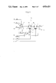
- FIG. 2 is a diagram showing circuit structure of each of the scan registers 14 in the scan-path shown in FIG. 1.
- the scan register 14 comprises a first latch circuit 1a, a second latch circuit 1b and a selector circuit 7, and operates by a two-phase clock.
- the selector circuit 7 has a first input terminal a connected to a serial input terminal 9, a second input terminal b connected to a parallel input terminal 10, a control terminal c connected to a selector control terminal 8 and an output terminal d.
- the first latch circuit 1a has an input terminal D connected to the output terminal d of the selector circuit 7, an enable terminal EN connected to a first clock terminal 5 and an output terminal Q.
- the second latch circuit 1b has an input terminal D connected to the output terminal Q of the first latch circuit 1a, an enable terminal EN connected to a second clock terminal 6 and an output terminal Q connected to a parallel output terminal 11 and a serial output terminal 12. Either one of the serial input terminal 9 and the parallel input terminal 10 is selected in response to a select signal SEL, so that data in the selected input terminal is applied to the input terminal D of the first circuit 1a through the output terminal d. Data applied to the input terminal D is latched in the latch circuit 1 a in response to a first clock signal CK1, and outputted from the output terminal Q. Thereafter, the data latched in the first latch circuit 1a is latched in the second latch circuit 1b in response to a second clock signal CK2, and outputted from the output terminal Q.
- the two-phase clock is applied to the first and second clock terminals 5 and 6, so that data applied to the serial input terminal 9 or the parallel input terminal 10 can be transferred to the serial output terminal 12 and the parallel output terminal 11, whereby a 1-bit shift operation is performed.
- n scan registers 15 shown in FIG. 1 are connected in series, thereby forming a scan-path.
- FIG. 3 is a circuit diagram showing another example of the conventional scan-path employed as a test auxiliary circuit.
- the scan-path comprises n scan registers 15 connected in series.
- Each of the scan registers 15 comprises a parallel clock terminal 5a, a serial clock terminal 5b, a second clock terminal 6, a serial input terminal 9, a parallel input terminal 10, a parallel output terminal 11 and a serial output terminal 12.
- the serial output terminal 12 of each of the scan registers 15 is connected to the serial input terminal 9 of an adjacent scan register 15.
- the parallel clock terminals 5a of the n scan registers 15 are connected to each other to receive a common parallel clock signal PCK1, and the serial clock terminals 5b thereof are connected to each other to receive a common serial clock signal SCK1.
- the second clock terminals 6 of the scan registers 15 are connected to each other to receive a common second clock signal CK2.
- the scan-path performs a parallel shift operation when the clock signal PCK1 is applied to the parallel clock terminals 5a while performing a serial shift operation when the clock signal SCK1 is applied to the serial clock terminals 5b.
- FIG. 4 is a diagram showing circuit structure of each of the scan registers 15 in the scan-path shown in FIG. 3.
- the scan register 15 is formed by an MOS circuit, which comprises a first ratio-type latch circuit 1c, a second ratio-type latch circuit 1d and three N channel transistors 13a, 13b and 13c.
- Each of the first and second ratio-type latch circuits 1c and 1d comprises two NOT circuits.
- An input terminal p of the ratio-type latch circuit 1c is connected to a parallel input terminal 10 through the transistor 13a, and to a serial input terminal 9 through the transistor 13b.
- the transistor 13a has its gate connected to a parallel clock terminal 5a
- the transistor 13b has its gate connected to a serial clock terminal 5b.
- the transistor 13c is connected between an output terminal q of the ratio-type latch circuit 1c and an input terminal p of the second ratio-type latch circuit 1d, and has its gate connected to a second clock terminal 6.
- a two-phase clock is applied to the parallel clock terminal 5a and the second clock terminal 6 or the serial clock terminal 5b and the second clock terminal 6, so that data applied to the parallel input terminal 10 or the serial input terminal 9 can be transferred to the parallel output terminal 11 and the serial output terminal 12, whereby a 1-bit shift operation can be performed.
- n scan registers 15 are connected in series, thereby forming the scan-path shown in FIG. 3.
- FIG. 5 is a diagram showing an example of a case in which a scan-path is connected to a data output terminal of a RAM.
- a circuit under test is the RAM.
- the scan-path comprises n scan registers 16 connected in series. Each of the scan registers 16 corresponds to each of the scan registers 14 or each of the scan registers 15 shown in FIGS. 1 to 4.
- a RAM 17 has n data output terminals 18.
- a parallel input terminal 10 of each of the scan registers 16 is connected to a corresponding data output terminal 18 of the RAM 17.
- the scan-path is formed on the same semiconductor chip as that on which the RAM 17 is formed.
- Output data Q 1 to Q n from the data output terminals 18 of the RAM 17 are accepted in the scan-path from parallel input terminals 10 by a parallel shift operation while being read out bit by bit from a serial output terminal 12 by a serial shift operation. Quality is determined by a testing device in response to the data as read out. This operation is performed with respect to all the addresses.
- An object of the present invention is to reduce the test time of a circuit under test in which data "0" or "1" are continuously read out.
- Another object of the present invention is to provide a test auxiliary circuit in which tests of the above described circuit under test can be performed by a small number of times of serial shift operations.
- Still another object of the present invention is to provide at low cost a semiconductor device comprising a test auxiliary circuit in which tests can be performed in a short time.
- the test auxiliary circuit employed for testing a semiconductor device comprises a plurality of data holding means, a plurality of parallel data input terminals, a serial data input terminal, and a serial data output terminal.
- the plurality of data holding means are connected in series and each can hold data.
- the plurality of parallel data input terminals are provided corresponding to the plurality of data holding means and each coupled to each of the data holding means.
- the serial data input terminal is coupled to data holding means in the first stage, of the plurality of data holding means.
- the serial data output terminal is coupled to the data holding means in the final stage, of the plurality of data holding means.
- each of the data holding means can transfer the data held therein to the data holding means in the subsequent stages, and holds data applied to a corresponding one of the parallel data input terminals in place of the data held therein if the data applied to the parallel data input terminal is different from the data held therein.
- a testing method comprises the following steps: Expected value data to be outputted from the semiconductor device if the semiconductor device is normal is serially inputted to the plurality of data holding means from the serial data input terminal to be held therein. The data outputted from the semiconductor device is applied to the plurality of parallel data input terminals. If the data applied to each of the parallel data input terminals is different from the expected value data held in each of the data holding means, data applied to the parallel data input terminal is held in place of the expected value data. After all data are outputted from the semiconductor device, the data held in the plurality of data holding means are outputted from the serial data output terminal.
- the test auxiliary circuit when data outputted from the circuit under test are applied to the parallel data input terminals with the expected value data being held in each of the data holding means, the data held by the holding means is inverted if the data is different from the expected value data.
- the data held in the plurality of data holding means are read out from the serial data output terminal by a serial shift operation after all the data in the circuit under test are outputted, it can be determined whether the circuit under test is good or bad depending on whether or not any of the expected value data is inverted.
- serial shift operation need not be performed every time the data is outputted from the circuit under test.
- FIG. 1 is a diagram showing an example of a conventional scan-path employed as a test auxiliary circuit
- FIG. 2 is a circuit diagram showing structure of each of scan registers constituting the scan-path shown in FIG. 1;
- FIG. 3 is a diagram showing another example of the conventional scan-path employed as the text auxiliary circuit
- FIG. 4 is a circuit diagram showing structure of each of scan registers constituting the scan-path shown in FIG. 3;
- FIG. 5 is a diagram showing a RAM chip comprising the conventional scan-path
- FIG. 6 is a diagram showing a scan-path employed as a test auxiliary circuit, according to an embodiment of the present invention.
- FIG. 7 is a circuit diagram showing structure of each of scan registers constituting the scan-path shown in FIG. 6;
- FIG. 8 is a diagram showing a scan-path employed as a test auxiliary circuit, according to another embodiment of the present invention.
- FIG. 9 is a circuit diagram showing structure of each of scan registers constituting the scan-path shown in FIG. 8.
- FIG. 10 is a diagram showing a RAM chip comprising the scan-path according to the embodiments of the present invention.
- FIG. 6 is a diagram showing structure of a scan-path employed as a test auxiliary circuit, according to an embodiment of the present invention.
- the scan-path comprises n scan registers 14 connected in series.
- Each of the scan registers 14a comprises a first clock terminal 5, a second clock terminal 6, a selector control terminal 8, a serial input terminal 9, a parallel input terminal 10, a parallel output terminal 11 and a serial output terminal 12, similarly to the scan register 14 shown in FIG. 1, and further comprises a test clock terminal 22.
- the serial output terminal 12 of the scan register 14a is connected to the serial input terminal 9 of an adjacent scan register 14a.
- the selector control terminals 8 of the n scan registers 14 are connected to each other, to receive a common select signal SEL.
- the first clock terminals 5 and the second clock terminals 6 of the scan registers 14a are connected to each other, respectively, to receive a common first clock signal CK1 and a common clock signal CK2, respectively.
- the test clock terminals 22 of the scan registers 14a are connected to each other, to receive a common clock test signal TCK1.
- the scan register 14a comprises a first latch circuit 1a, a second latch circuit 1b and a selector circuit 7, similar to the scan register 14 shown in FIG. 2, and further comprises an exclusive NOR (Ex. NOR) circuit 19, an NOR circuit 20 and an OR circuit 21.
- NOR exclusive NOR
- the scan register 14a shown in FIG. 7 is the same as the scan register 14 shown in FIG. 2 except for the following.
- the same or corresponding portions have the same reference numerals.
- the Ex.NOR circuit 19 has one input terminal connected to a parallel input terminal 10, another input terminal connected to an output terminal Q of the second latch circuit 1b, and an output terminal.
- the NOR circuit 20 has one input terminal connected to the output terminal of the Ex.NOR circuit 19, another input terminal connected to a test clock terminal 22, and an output terminal.
- An OR circuit 21 has one input terminal connected to the output terminal of the NOR circuit 20, another input terminal connected to a first clock terminal 5 and an output terminal connected to an enable terminal EN of the first latch circuit 1a.
- the scan register 14a When a test clock signal TCK1 is at a high level, the output of the NOR circuit 20 attains a low level, so that the OR circuit 21 directly transmits a first clock signal CK1 applied to the first clock terminal 5 to an enable terminal 4 of the latch circuit 1a.
- the scan register 14a performs the same operation as that of the conventional scan register 14 shown in FIG. 2. More specifically, either one of the serial input terminal 9 or the parallel input terminal 10 is selected in response to a select signal SEL, so that data in the selected input terminal is applied to an input terminal D of the first latch circuit 1a through an output terminal d.
- Data applied to the input terminal D is latched in the latch circuit 1a in response to a first clock signal CK1, and outputted from an output terminal Q. Thereafter, data latched in the first latch circuit 1a is latched in the second latch circuit 1b in response to a second clock signal CK2, and outputted from the output terminal Q.
- the test clock signal TCK1 is made to be a low level, and expected value data are set in the first and second latch circuits 1a and 1b. If data PI in the parallel input terminal 10 is different from the expected value data held in the second latch circuit 1b, the output of the Ex.NOR circuit 19 attains a low level. In this state, when a negative clock signal is applied to the test clock terminal 22, a positive clock signal is outputted from the NOR circuit 20.
- the scan-path shown in FIG. 6 comprising the scan register 14a shown in FIG. 7 performs the same operation as that of the conventional scan-path shown in FIG. 1. More specifically, the scan-path is responsive to the select signal SEL for performing a serial shift operation or a parallel shift operation in synchronization with the first and second clock signals CK1 and CK2 (a two-phase clock).
- test clock signal TCK1 of a low level is applied to the test clock terminal 22 with the expected value data being set in the scan registers 14a in the scan-path shown in FIG. 6, data held in the scan registers 14a are inverted only when the data PI applied to each of the parallel input terminals 10 is different from the expected value data.
- the scan register 14a stores the fact that the data PI applied to the parallel input terminal 10 is different from the expected value data.
- FIG. 8 is a diagram showing structure of a scan-path employed as a test auxiliary circuit, according to another embodiment of the present invention.
- the scan-path includes n scan registers 15a connected in series.
- Each of the scan registers 15a comprises a parallel clock terminal 5a, a serial clock terminal 5b, a second clock terminal 6, a serial input terminal 9, a parallel input terminal 10, a parallel output terminal 11 and a serial output terminal 12, similarly to the scan register 15 shown in FIG. 3, and further comprises a test clock terminal 22.
- the serial output terminal 12 of each of the scan registers 15a is connected to the serial input terminal 9 of an adjacent scan register 15.
- the parallel clock terminals 5a of the n scan registers 15 are connected to each other, to receive a common parallel clock signal PCK1, and the serial clock terminals 5b thereof are connected to each other, to receive a common serial clock signal SCK1.
- the second clock terminals 6 of the scan registers 15a are connected to each other, to receive a common second clock signal CK2.
- the test clock terminals 22 of the scan registers 15a are connected to each other, to receive a test clock signal TCK1.
- the scan register 15a is formed by an MOS circuit, which comprises a first ratio-type latch circuit 1c, a second ratio-type latch circuit 1d and three N channel transistors 13a, 13b and 13c, similarly to the scan register 15 shown in FIG. 4, and further comprises an exclusive NOR (Ex.NOR) circuit 19, and an NOR circuit 20 and an N channel transistor 13d.
- MOS circuit which comprises a first ratio-type latch circuit 1c, a second ratio-type latch circuit 1d and three N channel transistors 13a, 13b and 13c, similarly to the scan register 15 shown in FIG. 4, and further comprises an exclusive NOR (Ex.NOR) circuit 19, and an NOR circuit 20 and an N channel transistor 13d.
- NOR exclusive NOR
- the scan register 15a shown in FIG. 9 is the same as the scan register 15 shown in FIG. 4 except for the following. Therefore, the same or corresponding portions have the same reference numerals. More specifically, the Ex.NOR circuit 19 has one input terminal connected to a parallel input terminal 10, another input terminal connected to an output terminal q of the second ratio-type latch circuit 1d, and an output terminal. The NOR circuit 20 has one input terminal connected to the output terminal of the Ex.NOR circuit 19, another input terminal connected to a test clock terminal 22, and an output terminal. The transistor 13d is connected between an input terminal p of the first ratio-type latch circuit 1c and the parallel input terminal 10, and has its gate connected to the output terminal of the NOR circuit 20.
- the test clock signal TCK1 is made to be a low level, and expected value data are set in the first and second ratio-type latch circuits 1c and 1d. If data PI in the parallel input terminal 10 is different from the expected value data held in the second ratio-type latch circuit 1d, the output of the Ex.NOR circuit 19 attains a low level. In this state, when a negative clock signal is applied to the test clock terminal 22, a positive clock signal is outputted from the NOR circuit 20. Consequently, the transistor 13d is turned on, so that the data PI applied to the parallel input terminal 10 is latched in the first ratio-type latch circuit 1c. As a result, the content stored in the first latch circuit 1c is inverted.
- the output of the Ex.NOR circuit 19 attains a high level. Consequently, the output of the NOR circuit 20 attains a low level, so that the transistor 13d is turned off. Thus, the state of the first latch circuit 1c does not change.
- the scan-path shown in FIG. 8 comprising the scan register 15a shown in FIG. 9 performs the same operation as that of the conventional scan-path shown in FIG. 3. More specifically, the scan-path performs a parallel shift operation when the clock signal PCK1 is applied to the parallel clock terminal 5a while performing a serial shift operation when the clock signal SCK1 is applied to the serial clock terminal 5b.
- test clock signal TCK1 of a low level is applied to the test clock terminal 22 with the expected value data being set in the scan registers 15a in the scan-path shown in FIG. 8, data held in the scan registers 15a is inverted if data PI applied to each of the parallel input terminals 10 is different from the expected value data.
- the scan register 15a stores the fact that the data PI applied to the parallel input terminal 10 is different from the expected value data.
- the scan-path shown in FIGS. 6 and 8 whether or not different data from the expected value data is applied to the parallel input terminal 10.
- the circuit under test is a RAM and particularly, the scan-path according to the above described embodiments is connected to the data output terminals of the RAM, the marked effect is obtained.
- FIG. 10 is a diagram showing an example of a case in which a scan-path is connected to data output terminals 18 of the RAM.
- the scan-path comprises n scan registers 16 connected in series. Each of the scan registers 16a corresponds to the scan register 14a or 15a shown in FIGS. 6 to 9. A parallel input terminal 10 of each of the scan registers 16a is connected to a corresponding data output terminal 18 of an RAM 17.
- the scan-path is formed on the same semiconductor chip CH as that on which the RAM 17 is formed. In FIG. 10, the first and second clock terminals 5 and 6 or the parallel and serial clock terminals 5a and 6a and the second clock terminal 8 are omitted.
- the same data (data "0” or "1") are written to all addresses in the RAM 17 from a data input terminal (not shown).
- the data as written are read out from the output terminal 18. If the RAM 17 is normal, the same data are continuously read out.
- Expected value data are set in the scan-path from a serial input terminal 9 by a serial shift operation.
- the expected value data are data to be read out from the RAM 17 if the RAM 17 is normal. For example, if data "1" are written to all the addresses in the RAM 17, the expected value data are "1". Thereafter, every time data is read out from the RAM 17, a test clock signal TCK1 is applied to a test clock terminal 22. On this occasion, if different data from the expected value data is applied to the parallel input terminal 10 because the RAM 17 is defective, an internal latch of the scan register 16a to which the different data is applied is inverted. Thus, the test clock signal TCK1 is applied to the test clock terminal 22 with data being read out from the RAM 17.
- output data Q 1 to Q n from the RAM 17 need not be read out for every address by the serial shift operation, so that it is necessary to perform the serial shift operation only when expected value data are first written to the scan-path and finally data in the scan-path are read out.
- test auxiliary circuit may be applied to a circuit which continuously outputs same data "0" or "1", to obtain the marked effect.
- N channel transistors 13a to 13d are employed as the scan registers shown in FIG. 9, P channel transistors may be employed.
- the ratio-type latch circuits 1c and 1d may be replaced with latch circuits of another type, to obtain the same effect as that of the above described embodiment.
- the number of times of serial shift operations required for reading out response data of the circuit under test can be decreased, so that the test cost is reduced, whereby a low cost semiconductor device is obtained.
Landscapes
- Engineering & Computer Science (AREA)
- General Engineering & Computer Science (AREA)
- Physics & Mathematics (AREA)
- General Physics & Mathematics (AREA)
- Tests Of Electronic Circuits (AREA)
- Techniques For Improving Reliability Of Storages (AREA)
- Test And Diagnosis Of Digital Computers (AREA)
Applications Claiming Priority (2)
| Application Number | Priority Date | Filing Date | Title |
|---|---|---|---|
| JP62146622A JPH071493B2 (ja) | 1987-06-11 | 1987-06-11 | テスト補助回路 |
| JP62-146622 | 1987-06-11 |
Publications (1)
| Publication Number | Publication Date |
|---|---|
| US4926424A true US4926424A (en) | 1990-05-15 |
Family
ID=15411900
Family Applications (1)
| Application Number | Title | Priority Date | Filing Date |
|---|---|---|---|
| US07/207,919 Expired - Fee Related US4926424A (en) | 1987-06-11 | 1988-06-10 | Test auxiliary circuit for testing semiconductor device |
Country Status (2)
| Country | Link |
|---|---|
| US (1) | US4926424A (ja) |
| JP (1) | JPH071493B2 (ja) |
Cited By (14)
| Publication number | Priority date | Publication date | Assignee | Title |
|---|---|---|---|---|
| US5046047A (en) * | 1989-02-10 | 1991-09-03 | Plessey Overseas Limited | Circuit arrangement for verifying data stored in a random access memory |
| DE4202623A1 (de) * | 1991-02-25 | 1992-09-03 | Mitsubishi Electric Corp | Abtastpfadeinrichtung und eine integrierte halbleiterschaltkreiseinrichtung mit dieser |
| US5197070A (en) * | 1989-09-29 | 1993-03-23 | Mitsubishi Denki Kabushiki Kaisha | Scan register and testing circuit using the same |
| US5483492A (en) * | 1991-10-11 | 1996-01-09 | Sgs-Thomson Microelectronics S.A. | Method and apparatus for checking post-erasure contents of an erasable permanent memory |
| US5790891A (en) * | 1996-01-11 | 1998-08-04 | Galileo Technology Ltd. | Synchronizing unit having two registers serially connected to one clocked elements and a latch unit for alternately activating the registers in accordance to clock signals |
| EP0865046A2 (en) * | 1997-03-12 | 1998-09-16 | Information Storage Devices, Inc. | Analog signal recording and playback integrated circuit and message management system |
| US5815512A (en) * | 1994-05-26 | 1998-09-29 | Mitsubishi Denki Kabushiki Kaisha | Semiconductor memory testing device |
| US6041427A (en) * | 1997-10-27 | 2000-03-21 | Vlsi Technology | Scan testable circuit arrangement |
| US6260164B1 (en) | 1998-07-31 | 2001-07-10 | International Business Machines Corporation | SRAM that can be clocked on either clock phase |
| US6378108B1 (en) * | 1998-01-27 | 2002-04-23 | Stmicroelectronics S.A. | Parity checking circuit |
| EP1251520A2 (en) * | 2001-04-21 | 2002-10-23 | Hewlett-Packard Company | Random access memory |
| US6516431B1 (en) * | 1999-06-28 | 2003-02-04 | Mitsubishi Denki Kabushiki Kaisha | Semiconductor device |
| DE19519453B4 (de) * | 1994-05-26 | 2004-06-09 | Mitsubishi Denki K.K. | Halbleiterspeicher-Testvorrichtung |
| US20090319867A1 (en) * | 2008-06-24 | 2009-12-24 | Kabushiki Kaisha Toshiba | Memory system and memory access method |
Families Citing this family (3)
| Publication number | Priority date | Publication date | Assignee | Title |
|---|---|---|---|---|
| US6405335B1 (en) | 1998-02-25 | 2002-06-11 | Texas Instruments Incorporated | Position independent testing of circuits |
| US6728915B2 (en) | 2000-01-10 | 2004-04-27 | Texas Instruments Incorporated | IC with shared scan cells selectively connected in scan path |
| US6769080B2 (en) | 2000-03-09 | 2004-07-27 | Texas Instruments Incorporated | Scan circuit low power adapter with counter |
Citations (3)
| Publication number | Priority date | Publication date | Assignee | Title |
|---|---|---|---|---|
| US4601034A (en) * | 1984-03-30 | 1986-07-15 | Texas Instruments Incorporated | Method and apparatus for testing very large scale integrated memory circuits |
| US4698830A (en) * | 1986-04-10 | 1987-10-06 | International Business Machines Corporation | Shift register latch arrangement for enhanced testability in differential cascode voltage switch circuit |
| US4761768A (en) * | 1985-03-04 | 1988-08-02 | Lattice Semiconductor Corporation | Programmable logic device |
-
1987
- 1987-06-11 JP JP62146622A patent/JPH071493B2/ja not_active Expired - Lifetime
-
1988
- 1988-06-10 US US07/207,919 patent/US4926424A/en not_active Expired - Fee Related
Patent Citations (3)
| Publication number | Priority date | Publication date | Assignee | Title |
|---|---|---|---|---|
| US4601034A (en) * | 1984-03-30 | 1986-07-15 | Texas Instruments Incorporated | Method and apparatus for testing very large scale integrated memory circuits |
| US4761768A (en) * | 1985-03-04 | 1988-08-02 | Lattice Semiconductor Corporation | Programmable logic device |
| US4698830A (en) * | 1986-04-10 | 1987-10-06 | International Business Machines Corporation | Shift register latch arrangement for enhanced testability in differential cascode voltage switch circuit |
Non-Patent Citations (2)
| Title |
|---|
| 1985 Internation Test Conference: "A New Parallel Test Approach for Large Memories" by a R. Sridhar, paper No. 13.5, 1985, pp. 462-470. |
| 1985 Internation Test Conference: A New Parallel Test Approach for Large Memories by a R. Sridhar, paper No. 13.5, 1985, pp. 462 470. * |
Cited By (20)
| Publication number | Priority date | Publication date | Assignee | Title |
|---|---|---|---|---|
| US5046047A (en) * | 1989-02-10 | 1991-09-03 | Plessey Overseas Limited | Circuit arrangement for verifying data stored in a random access memory |
| US5197070A (en) * | 1989-09-29 | 1993-03-23 | Mitsubishi Denki Kabushiki Kaisha | Scan register and testing circuit using the same |
| DE4202623A1 (de) * | 1991-02-25 | 1992-09-03 | Mitsubishi Electric Corp | Abtastpfadeinrichtung und eine integrierte halbleiterschaltkreiseinrichtung mit dieser |
| US5483492A (en) * | 1991-10-11 | 1996-01-09 | Sgs-Thomson Microelectronics S.A. | Method and apparatus for checking post-erasure contents of an erasable permanent memory |
| US5815512A (en) * | 1994-05-26 | 1998-09-29 | Mitsubishi Denki Kabushiki Kaisha | Semiconductor memory testing device |
| DE19519453B4 (de) * | 1994-05-26 | 2004-06-09 | Mitsubishi Denki K.K. | Halbleiterspeicher-Testvorrichtung |
| US5946247A (en) * | 1994-05-26 | 1999-08-31 | Mitsubishi Denki Kabushiki Kaisha | Semiconductor memory testing device |
| US5790891A (en) * | 1996-01-11 | 1998-08-04 | Galileo Technology Ltd. | Synchronizing unit having two registers serially connected to one clocked elements and a latch unit for alternately activating the registers in accordance to clock signals |
| EP0865046A2 (en) * | 1997-03-12 | 1998-09-16 | Information Storage Devices, Inc. | Analog signal recording and playback integrated circuit and message management system |
| EP0865046A3 (en) * | 1997-03-12 | 1999-08-04 | Information Storage Devices, Inc. | Analog signal recording and playback integrated circuit and message management system |
| US6041427A (en) * | 1997-10-27 | 2000-03-21 | Vlsi Technology | Scan testable circuit arrangement |
| US6304988B1 (en) * | 1997-10-27 | 2001-10-16 | Philips Semiconductors, Inc. | Scan testable circuit arrangement |
| US6378108B1 (en) * | 1998-01-27 | 2002-04-23 | Stmicroelectronics S.A. | Parity checking circuit |
| US6260164B1 (en) | 1998-07-31 | 2001-07-10 | International Business Machines Corporation | SRAM that can be clocked on either clock phase |
| US6516431B1 (en) * | 1999-06-28 | 2003-02-04 | Mitsubishi Denki Kabushiki Kaisha | Semiconductor device |
| EP1251520A3 (en) * | 2001-04-21 | 2003-07-23 | Hewlett-Packard Company | Random access memory |
| EP1251520A2 (en) * | 2001-04-21 | 2002-10-23 | Hewlett-Packard Company | Random access memory |
| CN1332394C (zh) * | 2001-04-21 | 2007-08-15 | 惠普公司 | 多功能串行输入/输出电路 |
| US20090319867A1 (en) * | 2008-06-24 | 2009-12-24 | Kabushiki Kaisha Toshiba | Memory system and memory access method |
| US8166356B2 (en) * | 2008-06-24 | 2012-04-24 | Kabushiki Kaisha Toshiba | Memory system and memory access method |
Also Published As
| Publication number | Publication date |
|---|---|
| JPH071493B2 (ja) | 1995-01-11 |
| JPS63310046A (ja) | 1988-12-19 |
Similar Documents
| Publication | Publication Date | Title |
|---|---|---|
| US4926424A (en) | Test auxiliary circuit for testing semiconductor device | |
| US4914379A (en) | Semiconductor integrated circuit and method of testing same | |
| US4995039A (en) | Circuit for transparent scan path testing of integrated circuit devices | |
| KR0131185B1 (ko) | 논리회로 | |
| US4802163A (en) | Test-facilitating circuit and testing method | |
| KR940004653A (ko) | 반도체 메모리 장치 | |
| US4974226A (en) | Circuit for testing integrated circuits | |
| US4692901A (en) | Semiconductor memory | |
| JP2833563B2 (ja) | 半導体記憶装置 | |
| JP2003346500A (ja) | 半導体集積回路及びそのテスト方法 | |
| US4969126A (en) | Semiconductor memory device having serial addressing and operating method thereof | |
| US5384533A (en) | Testing method, testing circuit and semiconductor integrated circuit having testing circuit | |
| US6854078B2 (en) | Multi-bit test circuit | |
| US4742293A (en) | Pseudo-memory circuit for testing for stuck open faults | |
| US7246279B2 (en) | Static random access memory (SRAM) unit and method for operating the same | |
| US5894213A (en) | Semiconductor integrated circuit having a plurality of flip-flops | |
| US4913557A (en) | Intergrated logic circuit having testing function circuit formed integrally therewith | |
| US5197070A (en) | Scan register and testing circuit using the same | |
| US4829237A (en) | Circuit device having a self-testing function and a testing method thereof | |
| US5757818A (en) | Method and apparatus for scan out testing of integrated circuits with reduced test circuit area | |
| US5848075A (en) | Test device employing scan path having circuitry at switches between a scan in signal transmitted and previously held at a predetermined clock timing | |
| US5754758A (en) | Serial memory interface using interlaced scan | |
| US6898133B2 (en) | Package map data outputting circuit of semiconductor memory device and method for outputting package map data | |
| US6463562B1 (en) | Semiconductor device including macros and its testing method | |
| US6519726B1 (en) | Semiconductor device and testing method of the same |
Legal Events
| Date | Code | Title | Description |
|---|---|---|---|
| AS | Assignment |
Owner name: MITSUBUISHI DENKI KABUSHIKI KAISHA, 2-3 MARUNOUCHI Free format text: ASSIGNMENT OF ASSIGNORS INTEREST.;ASSIGNOR:MAENO, HIDESHI;REEL/FRAME:004902/0007 Effective date: 19880530 Owner name: MITSUBUISHI DENKI KABUSHIKI KAISHA,JAPAN Free format text: ASSIGNMENT OF ASSIGNORS INTEREST;ASSIGNOR:MAENO, HIDESHI;REEL/FRAME:004902/0007 Effective date: 19880530 |
|
| FEPP | Fee payment procedure |
Free format text: PAYOR NUMBER ASSIGNED (ORIGINAL EVENT CODE: ASPN); ENTITY STATUS OF PATENT OWNER: LARGE ENTITY |
|
| FPAY | Fee payment |
Year of fee payment: 4 |
|
| FPAY | Fee payment |
Year of fee payment: 8 |
|
| REMI | Maintenance fee reminder mailed | ||
| LAPS | Lapse for failure to pay maintenance fees | ||
| STCH | Information on status: patent discontinuation |
Free format text: PATENT EXPIRED DUE TO NONPAYMENT OF MAINTENANCE FEES UNDER 37 CFR 1.362 |
|
| FP | Lapsed due to failure to pay maintenance fee |
Effective date: 20020515 |