US4901151A - Television receiving section with digital stages - Google Patents
Television receiving section with digital stages Download PDFInfo
- Publication number
- US4901151A US4901151A US07/288,550 US28855088A US4901151A US 4901151 A US4901151 A US 4901151A US 28855088 A US28855088 A US 28855088A US 4901151 A US4901151 A US 4901151A
- Authority
- US
- United States
- Prior art keywords
- signal
- output
- input
- stage
- decimator
- Prior art date
- Legal status (The legal status is an assumption and is not a legal conclusion. Google has not performed a legal analysis and makes no representation as to the accuracy of the status listed.)
- Expired - Fee Related
Links
- 230000005236 sound signal Effects 0.000 claims abstract description 6
- 239000002131 composite material Substances 0.000 claims abstract description 3
- 238000005070 sampling Methods 0.000 claims description 9
- 230000001419 dependent effect Effects 0.000 claims description 3
- 238000005516 engineering process Methods 0.000 description 4
- 238000010586 diagram Methods 0.000 description 3
- 230000006978 adaptation Effects 0.000 description 2
- 238000004364 calculation method Methods 0.000 description 2
- 238000004519 manufacturing process Methods 0.000 description 2
- 238000006243 chemical reaction Methods 0.000 description 1
- 230000000694 effects Effects 0.000 description 1
- 239000004065 semiconductor Substances 0.000 description 1
Images
Classifications
-
- H—ELECTRICITY
- H04—ELECTRIC COMMUNICATION TECHNIQUE
- H04N—PICTORIAL COMMUNICATION, e.g. TELEVISION
- H04N5/00—Details of television systems
- H04N5/44—Receiver circuitry for the reception of television signals according to analogue transmission standards
-
- H—ELECTRICITY
- H04—ELECTRIC COMMUNICATION TECHNIQUE
- H04N—PICTORIAL COMMUNICATION, e.g. TELEVISION
- H04N5/00—Details of television systems
- H04N5/44—Receiver circuitry for the reception of television signals according to analogue transmission standards
- H04N5/60—Receiver circuitry for the reception of television signals according to analogue transmission standards for the sound signals
Definitions
- the present invention is in the field of digital television, and, more particularly, in the field of digital television receivers that receive a standard television broadcast signal in analog form and convert it to a digital representation for further processing of the signal in a digital form.
- A/D converters analog-to-digital converters
- One of the A/D converters serves to convert the video signal from analog to digital form and is commonly located after the so-called sound trap, which keeps the sound-carrier signal out of the remaining signal.
- This first A/D converter is operated with a sampling signal whose frequency is usually four times the chrominance subcarrier frequency.
- this first A/D converter is a flash converter.
- the second A/D converter is located at the beginning of the audio channel and, unlike the first-mentioned A/D converter, is generally a delta-sigma converter.
- the object of the invention as claimed to provide a circuit principle for television receiving sections having at least one interface between the analog signal processing circuitry and the digital signal-processing circuitry which permits considerably simpler adaptation to different television standards and reduces the number of A/D converters required.
- the main idea underlying the invention is to use a single A/D converter already at the output of the intermediate-frequency stage (i.e., where the signal, still in its analog format, lies in a frequency range between about 30 MHz and 40 MHz).
- the clock signal of this A/D converter has a frequency approximately equal to twice the bandwidth of the received signal (e.g., a frequency of about 20 MHz).
- the received signal is divided into a video-information-processing channel ("the video channel"), and an audio-information processing channel (“the audio channel”).
- the need for the separate audio-channel A/D converter is eliminated, so that in a currently marketable system, a complete integrated circuit is saved.
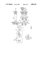
- FIG. 1 is a block diagram of an embodiment of the invention
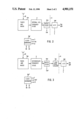
- FIG. 2 is a block diagram of a portion of the arrangement of FIG. 1 representing a development of the invention.
- FIG. 3. is a block diagram of a portion of the arrangement of FIG. 1 representing a further development of the invention.
- FIG. 1 shows the portion of a television receiver of video recorder to which the invention relates, namely the television receiving section.
- an antenna signal al is fed to a tuner and mixer tw, which is implemented in any of the conventional technologies.
- the tuner and mixer tw is followed by an intermediate-frequency stage z, which provides a video- and audio-information-containing signal v at the intermediate frequency.
- the video- and audio-information-containing signal v is converted by means of a single A/D converter aw, whose clock signal t has a frequency of about 20 MHz, into a digital signal whose frequency band extends from about 1 MHz to about 9 MHz.
- the clock signal t is generated by a clock generator tg.
- the output of the A/D converter aw feeds a video-information-processing channel vk, called "video channel”, and an audio-information-processing channel ak, called “audio channel”.
- the video channel vk includes a band-pass filter bp at its input end.
- the band-pass filter bp has a passband that extends between 1 MHz and 6 MHz.
- the bandpass filter bp has two outputs that are connected directly and through a 90° phase shifter ps, respectively, to the inputs of a first stage b1.
- the first stage b1 produces an output equal to the magnitude of the vector sum of its two input signals (i.e., the square root of the sum of the squares of its two input signals), and is henceforth called the "first absolute-value stage" b1.
- the output of the first absolute-value stage b1 provides a digital composite color signal fb.
- the audio channel ak includes a quadrature mixer qm at its input end.
- the quadrature mixer qm operates in response to two locally generated signals, a digital sine wave signal ss and a digital cosine-wave signal cs, which are generated by the clock generator tg and have the same television-standard-dependent fixed frequency (i.e., a frequency between 7 MHz and 7.5 MHz).
- the quadrature mixer qm comprises two multipliers m1, m2, which are fed with the digital sine-wave signal ss and the digital cosine-wave signal cs, respectively.
- Each of the two output signals of the quadrature mixer qm is converted by means of one of two decimators dI, d2 from the high frequency of the clock signal t to the lower frequency of a sampling signal d, also from the clock generator tg.
- the lower frequency is suitable for the subsequent signal-processing circuitry.
- the outputs of the two decimators d1, d2 are connected to the two inputs of a second stage b2 that produces an output equal to the magnitude of the vector sum of its input signals.
- the second stage b2 is henceforth called the “second absolute-value stage” b2.
- the outputs of the two decimators d1, d2 are also connected to the two inputs of a stage wb that computes the angle between its two input signals, and which is henceforth called the "angle-computing stage" wb.
- the angle-computing stage wb is followed by a differentiating stage dt, whose output provides a frequency-demodulated audio signal fa when such a signal is being received.
- the output of the second absolute-value stage b2 provides an amplitude-demodulated audio signal aa when such a signal is being received.
- the two absolute-value stages b1, b2 and the angle-computing stage wb are preferably circuits employing the CORDIC computing technique, as described, for example, in Jack E. Volder, "The CORDIC Trigonometric Computing Technique," IRE Transaction on Electronic Computers, September 1959, pp. 330-334.
- circuits following the two absolute-value stages b1, b2 and those following the differentiating stage dt are of the kind commonly used for digital signal processing in television receiving sections, and are not shown herein.
- FIG. 2 shows a development of the arrangement of FIG. 1 for the case where the frequencies at the output of the intermediate-frequency stage z are substantially higher than the frequency of the clock signal t of the A/D converter aw.
- the A/D converter aw must meet very high accuracy requirements because the variations in the sampling instant (the so-called aperture jitter) result in uncorrectable distortions of the A/D-converted signal.
- the mixer stage ms is interposed between the output of the intermediate-frequency stage z and the input of the A/D converter aw.
- the mixer stage ms is fed with a locally generated signal tm, whose frequency is an integral multiple of the frequency of the clock signal t. This latter measure prevents aliasing effects during the A/D conversion.
- the clock generator tg also generates the signal tm.
- FIG. 3 shows a further development of the arrangement of FIG. 1 for the case where the signal at the output of the intermediate-frequency stage z is already a band-limited signal.
- the locally generated signal tm of FIG. 2 is preferably a square-wave signal tm' (FIG. 3), from which the clock signal t can be derived by frequency division.
- the clock generator tg" of FIG. 3 then includes a frequency-divider circuit to generate the clock signal t.
- FIG. 3 also shows that it may be advantageous to place between the mixer stage ms and the A/D converter aw a low-pass filter tp, by which higher-frequency signal components at the output of the mixer stage ms are suppressed.
- the cutoff frequency of the low-pass filter tp must be chosen accordingly.
- the invention is preferably implemented with integrated circuits, using the specific technology best suited for the individual parts, i.e., both the best suited fabrication technology for the semiconductor chip and the best suited basic circuit technology.
Landscapes
- Engineering & Computer Science (AREA)
- Multimedia (AREA)
- Signal Processing (AREA)
- Circuits Of Receivers In General (AREA)
- Analogue/Digital Conversion (AREA)
- Superheterodyne Receivers (AREA)
Applications Claiming Priority (3)
| Application Number | Priority Date | Filing Date | Title |
|---|---|---|---|
| DE3743727 | 1987-12-23 | ||
| DE19873743727 DE3743727A1 (de) | 1987-12-23 | 1987-12-23 | Fernsehempfangsteil mit digital arbeitenden stufen |
| EP88118095 | 1988-10-31 |
Publications (1)
| Publication Number | Publication Date |
|---|---|
| US4901151A true US4901151A (en) | 1990-02-13 |
Family
ID=6343373
Family Applications (1)
| Application Number | Title | Priority Date | Filing Date |
|---|---|---|---|
| US07/288,550 Expired - Fee Related US4901151A (en) | 1987-12-23 | 1988-12-22 | Television receiving section with digital stages |
Country Status (3)
| Country | Link |
|---|---|
| US (1) | US4901151A (de) |
| EP (1) | EP0321681B1 (de) |
| DE (2) | DE3743727A1 (de) |
Cited By (9)
| Publication number | Priority date | Publication date | Assignee | Title |
|---|---|---|---|---|
| US4974086A (en) * | 1988-07-02 | 1990-11-27 | Deutsche Itt Industries Gmbh | Frequency conversion circuit for a color television channel |
| US5023609A (en) * | 1988-06-07 | 1991-06-11 | Deutsche Itt Industries Gmbh | Digital deemphasis circuit |
| US5130802A (en) * | 1990-02-15 | 1992-07-14 | U.S. Philips Corporation | Television receiving section having an a/d converter which simultaneously performs synchronous demodulation |
| US5202766A (en) * | 1987-11-06 | 1993-04-13 | Deutsche Itt Industries Gmbh | Sound channel circuit for digital television receivers |
| US5230011A (en) * | 1990-11-15 | 1993-07-20 | U.S. Philips Corporation | Receiver |
| US5416525A (en) * | 1992-08-11 | 1995-05-16 | Koninklijke Ptt Nederland N.V. | Method and apparatus for digitally coding and decoding a composite signal, containing baseband and out-of-band signals using relatively few bits and yielding a decoded out-of-band signal having increased quality |
| US5430890A (en) * | 1992-11-20 | 1995-07-04 | Blaupunkt-Werke Gmbh | Radio receiver for mobile reception with sampling rate oscillator frequency being an integer-number multiple of reference oscillation frequency |
| US6118499A (en) * | 1997-05-19 | 2000-09-12 | Mitsubishi Denki Kabushiki Kaisha | Digital television signal receiver |
| US20080175558A1 (en) * | 2005-05-24 | 2008-07-24 | Pixtree Technologis, Inc. | Hardware Apparatus and Method Having Video/Audio Encoding and Multiplexing Functionality |
Families Citing this family (8)
| Publication number | Priority date | Publication date | Assignee | Title |
|---|---|---|---|---|
| DE4128129C1 (de) * | 1991-08-24 | 1993-03-11 | Blaupunkt-Werke Gmbh, 3200 Hildesheim, De | |
| DE4417724A1 (de) * | 1994-05-20 | 1995-11-23 | Ant Nachrichtentech | Einrichtung zur digitalen Demodulation der Bild- und Tonanteile eines Fernsehsignals |
| DE4417723A1 (de) * | 1994-05-20 | 1995-11-23 | Ant Nachrichtentech | Einrichtung zum Verarbeiten eines modulierten reellwertigen analogen Fernsehsignals |
| DE4417725A1 (de) * | 1994-05-20 | 1995-11-23 | Ant Nachrichtentech | Einrichtung zur digitalen Demodulation der Bild- und Tonanteile eines Fernsehsignals |
| DE69621664T2 (de) * | 1995-01-23 | 2002-11-28 | Thomson Multimedia Sa | Schaltungsanordnung zur A/D-Umsetzung eines Videosignals mit Hoch- oder Zwischenfrequenz |
| EP0727878B1 (de) * | 1995-01-23 | 2002-06-12 | THOMSON multimedia | Schaltungsanordnung zur A/D-Umsetzung eines Videosignals mit Hoch- oder Zwischenfrequenz |
| FR2734681B1 (fr) * | 1995-05-23 | 1997-07-04 | Thomson Multimedia Sa | Procede pour numeriser un signal de frequence intermediaire fi, en particulier de television, et circuit pour la mise en oeuvre de ce procede |
| FR2735316B1 (fr) * | 1995-06-12 | 1997-07-18 | Thomson Multimedia Sa | Procede de numerisation de signaux video fi et dispositif pour mettre en oeuvre ce procede |
Citations (4)
| Publication number | Priority date | Publication date | Assignee | Title |
|---|---|---|---|---|
| US4709270A (en) * | 1985-06-01 | 1987-11-24 | Deutsche Itt Industries Gmbh | Circuit arrangement for filtering and demodulating a signal frequency-modulator with at least one audio signal |
| US4710814A (en) * | 1985-08-27 | 1987-12-01 | Deutsche Itt Industries Gmbh | Television sound receiving circuit for at least one sound channel contained in an RF signal |
| US4782385A (en) * | 1985-08-27 | 1988-11-01 | Deutsche Itt Industries Gmbh | Frequency conversion of an RF signal transmitted for color-television receivers |
| US4811096A (en) * | 1987-05-20 | 1989-03-07 | Sanyo Electric Co., Ltd. | Video detector employing PLL system |
Family Cites Families (2)
| Publication number | Priority date | Publication date | Assignee | Title |
|---|---|---|---|---|
| US4502078A (en) * | 1982-02-22 | 1985-02-26 | Rca Corporation | Digital television receivers |
| EP0237590B1 (de) * | 1986-03-15 | 1989-08-09 | Deutsche ITT Industries GmbH | Regelschaltung zur Regelung von zwei ca. 90o Phasenverschiebung aufweisenden Signalen |
-
1987
- 1987-12-23 DE DE19873743727 patent/DE3743727A1/de not_active Withdrawn
-
1988
- 1988-10-31 DE DE88118095T patent/DE3886717D1/de not_active Expired - Lifetime
- 1988-10-31 EP EP88118095A patent/EP0321681B1/de not_active Expired - Lifetime
- 1988-12-22 US US07/288,550 patent/US4901151A/en not_active Expired - Fee Related
Patent Citations (4)
| Publication number | Priority date | Publication date | Assignee | Title |
|---|---|---|---|---|
| US4709270A (en) * | 1985-06-01 | 1987-11-24 | Deutsche Itt Industries Gmbh | Circuit arrangement for filtering and demodulating a signal frequency-modulator with at least one audio signal |
| US4710814A (en) * | 1985-08-27 | 1987-12-01 | Deutsche Itt Industries Gmbh | Television sound receiving circuit for at least one sound channel contained in an RF signal |
| US4782385A (en) * | 1985-08-27 | 1988-11-01 | Deutsche Itt Industries Gmbh | Frequency conversion of an RF signal transmitted for color-television receivers |
| US4811096A (en) * | 1987-05-20 | 1989-03-07 | Sanyo Electric Co., Ltd. | Video detector employing PLL system |
Non-Patent Citations (2)
| Title |
|---|
| Jack E. Volder, "The CORDIC Trigonometric Computing Technique," IRE Transaction on Electronic Computers, Sep. 1959, pp. 330-334. |
| Jack E. Volder, The CORDIC Trigonometric Computing Technique, IRE Transaction on Electronic Computers, Sep. 1959, pp. 330 334. * |
Cited By (10)
| Publication number | Priority date | Publication date | Assignee | Title |
|---|---|---|---|---|
| US5202766A (en) * | 1987-11-06 | 1993-04-13 | Deutsche Itt Industries Gmbh | Sound channel circuit for digital television receivers |
| US5023609A (en) * | 1988-06-07 | 1991-06-11 | Deutsche Itt Industries Gmbh | Digital deemphasis circuit |
| US4974086A (en) * | 1988-07-02 | 1990-11-27 | Deutsche Itt Industries Gmbh | Frequency conversion circuit for a color television channel |
| US5130802A (en) * | 1990-02-15 | 1992-07-14 | U.S. Philips Corporation | Television receiving section having an a/d converter which simultaneously performs synchronous demodulation |
| US5230011A (en) * | 1990-11-15 | 1993-07-20 | U.S. Philips Corporation | Receiver |
| US5416525A (en) * | 1992-08-11 | 1995-05-16 | Koninklijke Ptt Nederland N.V. | Method and apparatus for digitally coding and decoding a composite signal, containing baseband and out-of-band signals using relatively few bits and yielding a decoded out-of-band signal having increased quality |
| US5430890A (en) * | 1992-11-20 | 1995-07-04 | Blaupunkt-Werke Gmbh | Radio receiver for mobile reception with sampling rate oscillator frequency being an integer-number multiple of reference oscillation frequency |
| US6118499A (en) * | 1997-05-19 | 2000-09-12 | Mitsubishi Denki Kabushiki Kaisha | Digital television signal receiver |
| US20080175558A1 (en) * | 2005-05-24 | 2008-07-24 | Pixtree Technologis, Inc. | Hardware Apparatus and Method Having Video/Audio Encoding and Multiplexing Functionality |
| US8041180B2 (en) * | 2005-05-24 | 2011-10-18 | Pixtree Inc. | Hardware apparatus and method having video/audio encoding and multiplexing functionality |
Also Published As
| Publication number | Publication date |
|---|---|
| DE3743727A1 (de) | 1989-07-13 |
| EP0321681B1 (de) | 1993-12-29 |
| EP0321681A2 (de) | 1989-06-28 |
| EP0321681A3 (de) | 1991-07-17 |
| DE3886717D1 (de) | 1994-02-10 |
Similar Documents
| Publication | Publication Date | Title |
|---|---|---|
| US4901151A (en) | Television receiving section with digital stages | |
| US7599006B2 (en) | Over-sampling A/D converting circuit | |
| USRE32188E (en) | Color television receiver comprising at least one integrated circuit for the luminance signal and the chrominance signals | |
| EP0335037A1 (de) | Direktmisch-Funkgerät | |
| KR20010099742A (ko) | 프론트앤드회로 | |
| JPH0354919B2 (de) | ||
| US4549201A (en) | Circuit arrangement for digitizing and storing color video signal | |
| WO2006119025A1 (en) | Nicam encoder with a front-end | |
| US4634989A (en) | Digital FM detector for a digital signal | |
| JPS60107932A (ja) | アナログ・デイジタル変換装置 | |
| JP2561336B2 (ja) | デジタル処理段を備えたテレビジョン受像装置 | |
| US20020105594A1 (en) | Signal processing apparatus | |
| US20020025007A1 (en) | Receiver | |
| EP0341989B1 (de) | Vorrichtung zur gleichzeitigen Ausgabe mehrerer von einem Videosignal abgeleiteter Bildsignale, mit einem einzigen Digital-Analog-Wandler | |
| US5303038A (en) | Circuit arrangement for A/D conversion of the color information components of two picture signals | |
| JPH07240938A (ja) | Y/c分離装置 | |
| US5192996A (en) | Video chroma signal processing circuit | |
| KR0141679B1 (ko) | 디지탈 콤필터의 고역 보상회로 | |
| US7199843B2 (en) | Spectral translation for VSB compensation | |
| JPH0360233B2 (de) | ||
| JPS60152192A (ja) | 映像信号のデイジタル処理回路 | |
| JP3069024B2 (ja) | Rgbエンコーダ | |
| KR920009183B1 (ko) | 비디오 데이타 압축을 위한 색차신호의 다운 샘플러 | |
| JPH0662432A (ja) | Ad変換装置 | |
| JPS6364489A (ja) | サンプリング周波数変換装置 |
Legal Events
| Date | Code | Title | Description |
|---|---|---|---|
| AS | Assignment |
Owner name: DEUTSCHE ITT INDUSTRIES GMBH, GERMANY Free format text: ASSIGNMENT OF ASSIGNORS INTEREST.;ASSIGNORS:MEHRGARDT, SONKE;EHRHARDT, DIETMAR;REEL/FRAME:005024/0215 Effective date: 19890213 |
|
| FEPP | Fee payment procedure |
Free format text: PAYOR NUMBER ASSIGNED (ORIGINAL EVENT CODE: ASPN); ENTITY STATUS OF PATENT OWNER: LARGE ENTITY |
|
| FPAY | Fee payment |
Year of fee payment: 4 |
|
| FEPP | Fee payment procedure |
Free format text: PAYOR NUMBER ASSIGNED (ORIGINAL EVENT CODE: ASPN); ENTITY STATUS OF PATENT OWNER: LARGE ENTITY Free format text: PAYER NUMBER DE-ASSIGNED (ORIGINAL EVENT CODE: RMPN); ENTITY STATUS OF PATENT OWNER: LARGE ENTITY |
|
| FPAY | Fee payment |
Year of fee payment: 8 |
|
| REMI | Maintenance fee reminder mailed | ||
| LAPS | Lapse for failure to pay maintenance fees | ||
| STCH | Information on status: patent discontinuation |
Free format text: PATENT EXPIRED DUE TO NONPAYMENT OF MAINTENANCE FEES UNDER 37 CFR 1.362 |
|
| FP | Lapsed due to failure to pay maintenance fee |
Effective date: 20020213 |