US4855596A - Photo ion spectrometer - Google Patents
Photo ion spectrometer Download PDFInfo
- Publication number
- US4855596A US4855596A US07/046,117 US4611787A US4855596A US 4855596 A US4855596 A US 4855596A US 4611787 A US4611787 A US 4611787A US 4855596 A US4855596 A US 4855596A
- Authority
- US
- United States
- Prior art keywords
- potential
- sample
- electric field
- field potential
- region
- Prior art date
- Legal status (The legal status is an assumption and is not a legal conclusion. Google has not performed a legal analysis and makes no representation as to the accuracy of the status listed.)
- Expired - Fee Related
Links
Images


Classifications
-
- H—ELECTRICITY
- H01—ELECTRIC ELEMENTS
- H01J—ELECTRIC DISCHARGE TUBES OR DISCHARGE LAMPS
- H01J49/00—Particle spectrometers or separator tubes
- H01J49/44—Energy spectrometers, e.g. alpha-, beta-spectrometers
- H01J49/46—Static spectrometers
- H01J49/48—Static spectrometers using electrostatic analysers, e.g. cylindrical sector, Wien filter
- H01J49/484—Static spectrometers using electrostatic analysers, e.g. cylindrical sector, Wien filter with spherical mirrors
-
- H—ELECTRICITY
- H01—ELECTRIC ELEMENTS
- H01J—ELECTRIC DISCHARGE TUBES OR DISCHARGE LAMPS
- H01J49/00—Particle spectrometers or separator tubes
- H01J49/02—Details
- H01J49/06—Electron- or ion-optical arrangements
- H01J49/061—Ion deflecting means, e.g. ion gates
-
- H—ELECTRICITY
- H01—ELECTRIC ELEMENTS
- H01J—ELECTRIC DISCHARGE TUBES OR DISCHARGE LAMPS
- H01J49/00—Particle spectrometers or separator tubes
- H01J49/02—Details
- H01J49/10—Ion sources; Ion guns
- H01J49/14—Ion sources; Ion guns using particle bombardment, e.g. ionisation chambers
- H01J49/142—Ion sources; Ion guns using particle bombardment, e.g. ionisation chambers using a solid target which is not previously vapourised
-
- H—ELECTRICITY
- H01—ELECTRIC ELEMENTS
- H01J—ELECTRIC DISCHARGE TUBES OR DISCHARGE LAMPS
- H01J49/00—Particle spectrometers or separator tubes
- H01J49/02—Details
- H01J49/10—Ion sources; Ion guns
- H01J49/16—Ion sources; Ion guns using surface ionisation, e.g. field-, thermionic- or photo-emission
- H01J49/161—Ion sources; Ion guns using surface ionisation, e.g. field-, thermionic- or photo-emission using photoionisation, e.g. by laser
-
- H—ELECTRICITY
- H01—ELECTRIC ELEMENTS
- H01J—ELECTRIC DISCHARGE TUBES OR DISCHARGE LAMPS
- H01J49/00—Particle spectrometers or separator tubes
- H01J49/26—Mass spectrometers or separator tubes
- H01J49/28—Static spectrometers
- H01J49/282—Static spectrometers using electrostatic analysers
Definitions
- the present invention relates generally to a charged particle spectrometer. More particularly the invention relates to an ion spectrometer having a lens system configured to extract from a sample ionized atomic components having well controlled energy and also to provide precise spatial manipulation of the various ion beams, enabling highly sensitive detection of the ionized atomic components. Improvement of signal to noise ratio is also achieved by exciting the atomic components to autoionization states before performing energy and angular refocusing time of flight (hereinafter, "EARTOF”) mass spectrometric analysis.
- EOTAF energy and angular refocusing time of flight
- a significant feature in accordance with the instant invention lies in the provision of an improved spectrometer having enhanced sensitivity for detecting selected atomic components of a sample.
- a lens system is configured to provide a predetermined slowly diminishing electric field region for a volume containing a large portion of the ionized form of the selected atomic components, thereby minimizing the energy spread of the volume of the ionized selected atomic components which are subsequently extracted for spectroscopic analysis, such as in an EARTOF spectrometer.
- the relatively small energy spread makes the spectroscopic analysis substantially more accurate and increases the signal to noise ratio.
- the lens system also applies a pulsed electric field to the sample to remove some of the unwanted secondary ions from the volume containing neutral ones of the selected atomic components prior to their ionization.
- the pulsed electric field also places some of the unwanted secondary ions into high energy escape orbits, causing the secondary ions to be rejected in subsequent stages of the spectrometer 10.
- the selected atomic components are excited to an ionized state, including selected autoionization states which provide enhanced discrimination of unwanted ionized species.
- the lens system is adapted to perform a number of different spatial manipulations of various charged particle beams.
- the lens system can guide a primary ion beam perpendicular to the surface of the sample, while also adapted for extracting ions of the selected atomic component perpendicular to the sample surface along a path leading to the detector at the end of the spectrometer.
- the final stages of the lens system include two complementary spherical electric field sections.
- a preselected resistive thick film configuration is disposed on an insulator substrate for generating predetermined electric field boundary conditions for any one of a number of uses.
- the resistive thick film configuration is used in conjunction with the spherical electrostatic analyzers, achieving the required electric field potential necessary for accurate EARTOF spectrometer analysis and minimization of signal loss.
- FIG. 1 illustrates an ion spectrometer constructed in accordance with one embodiment of the invention
- FIG. 2 shows a fragmentary view of the sample chamber and ion extraction region of the spectrometer of FIG. 1;
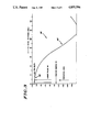
- FIG. 3 illustrates a predetermined electric field as a function of perpendicular distance from the sample area shown in FIG. 2;
- FIG. 4 is an enlarged fragmentary view of the sample area during generation of ions for analysis
- FIG. 5 illustrates a timing cycle for generation of an ionized beam of the selected atomic component
- FIG. 6A depicts the orbits in the electrostatic analyzer of ions having various energies and FIG. 6B illustrates the orbits of ions entering at different angles with the same energy;
- FIG. 7 shows a plan view of an example of the components of a preselected thick film configuration on an insulator substrate.
- the ion spectrometer 10 (hereinafter, the "spectrometer 10") includes a sample 14 disposed within a high vacuum (less than about 10 -9 Torr.) provided by a conventional ultra high vacuum pumping system (not shown). Measurement of the quantity of a selected atomic component from the sample 14 is carried out by removing atoms for subsequent quantitative analysis. The selected atomic component is removed from the sample 14 by irradiating the sample 14 with an energetic particle beam, such as an ionized particle beam 18 (hereinafter, "primary ion beam 18”) in the illustrated embodiment.
- an energetic particle beam such as an ionized particle beam 18 (hereinafter, "primary ion beam 18") in the illustrated embodiment.
- a substantial portion of the selected atomic component removed from the sample 14 originates from a sample region 15, shown in FIG. 4, wherein the flux is highest from the primary ion beam 18.
- inert gas ions are used as the primary ion beam 18 and have an energy of 5 kV.
- the primary ion beam 18 is preferably a pulsed beam (see FIG. 5) in order to cooperate with other physical events (some of which are shown in FIG. 5), enabling performance of various functionalities to be described hereinafter.
- the primary ion beam 18 is deflected by deflector plates 22 from a first path 26 to a second path 30, which intersects the sample 14 substantially perpendicular thereto.
- the energetic particle beam can be other types of beams, such as, for example, a neutral particle beam, an electron beam, fission fragments or a photon beam, such as a laser beam.
- a neutral particle beam an electron beam, fission fragments or a photon beam, such as a laser beam.
- a photon beam such as a laser beam.
- a positive electric field potential 32 is generated on the sample 14. As shown in FIG. 5, the positive electric field potential 32 on the sample 14 is pulsed from about +1080 to +1350 volts prior to the arrival of the 5 kV pulsed primary ion beam 18 at the sample 14. The electric field potential 32 is maintained throughout the period of sputtering atoms from the sample 14.
- the positive electric field potential 32 acts to: (1) remove stray ions present before the sputtering of atoms (or ejection of the atoms by other means) from the sample 14, and also (2) to remove any secondary ions present as a consequence of the sample irradiation by the primary ion beam 18.
- the volume near the sample 14 contains as a residual various neutral forms of the selected atomic components which the operator desires to detect. These selected atomic components are, for example, single atoms and molecules.
- the volume containing a large portion of the selected atomic components near the sample 14 is irradiated to generate photo ions.
- the irradiation is performed by a laser beam pulse 34 shown in an end view cross section. As shown in FIG. 5 the laser beam pulse 34 is timed subsequent to the removal of unwanted ions from near the sample 14.
- the laser beam pulse 34 is timed subsequent to the removal of unwanted ions from near the sample 14.
- the laser beam pulse 34 can comprise more than one pulse of different laser energies E 1 and E 2 , and this aspect of the invention will be described in more detail below.
- a perimeter 38 of a 45° conical volume is illustrated in FIG. 4, and the conical volume encompasses about one half of the ions ejected from the sample region 15 of the sample 14, assuming a cosine type distribution of the ions relative to the axis defined by the beam path 30 for the primary ion beam 18.
- the laser beam pulse 34 is therefore positioned with respect to this distribution to excite the maximum possible percentage of the neutral selected atomic components ejected from the sample 14.
- ions of the selected atomic components is an important early step toward the objective of isolating the desired signal from unwanted noise and extraneous signals measured during the final quantitative analysis. Therefore, sensitive analysis is commenced by the laser beam pulse 34 ionizing the selected atomic components to energies above the ionization potential (see FIG. 5). Significant further separation of the desired signal is achievable using two laser energies, E 1 and E 2 mentioned above, with the first part of the laser beam pulse 34 having an energy E 1 to selectively excite the selected atomic component to an energy below the ionization level. The second laser pulse 34 has the energy E 2 which ionizes the previously excited atomic component.
- excitation for E 2 is, for example, non-resonant excitation to the ionization continuum. Because the second laser energy at E 2 is not in energy resonance between an initial energy state and a final discrete state of the excited atomic component to be ionized, the cross section for the process is small; consequently, the power density required to saturate the ionization process is usually quite large. The required power can be achieved with large fixed-frequency lasers, but the drawback is that multiphoton non-resonant ionization of various unwanted species can become important.
- the multiphoton non-resonant ionization process may still have low probability relative to the single photon non-resonant ionization of the previously excited selected atomic component of interest, significant background ionization may still occur because of the much greater abundance of the majority species (e.g., atomic species of the matrix of the sample 14) in the ionization volume irradiated by the laser pulse 34.
- the majority species e.g., atomic species of the matrix of the sample 14
- a useful alternative for the second, ionization step at E 2 involves the application of specific wavelengths chosen to connect the excited atomic level at E 1 , produced by irradiation from the first laser pulse 34, with photon energy E 1 , to an autoionizing level of the selected atom component.
- States of the autoionization type are also conventionally called "discrete states embedded in the continuum", and have the property of rapidly decaying to an ion plus a free electron. Nevertheless, cross sections for excitation to these autoionization states are much larger than those for non-resonant ionization. Consequently, saturation of the second excitation step with energy E 2 is possible with the use of much less power density. This reduces the probability of ionizing majority unwanted species via multiphoton non-resonant ionization processes.
- Multiphoton non-resonant ionization refers to a physical process where more than one photon is absorbed by an atomic or molecular species, with all the photons being absorbed in a single step. To achieve the desired power levels, conventional focused, high power, non-tunable lasers are typically employed.
- a rapid survey of possible impurity species of the selected atomic component in the sample 14 can be performed. Since ionization occurs without the necessity of tuning to energy resonances of each species individually of the selected atomic component, ion signals from neutral precursors of all elements present is obtained upon each occurrence of the laser pulse 34. Separation by mass is performable by a time of flight mass spectrometer alone.
- the ion-production step is a laser-based, multiphoton ionization of gas phase species released from the sample by conventional ablation processes. Variation of ionization probability from one atomic species to another can be minimized and calibrated. Dependence on the chemical environment in the sample 14 is small since the process of sputtering material depends essentially on simple momentum-transfer considerations. In contrast, in other types of ion spectroscopy (such as secondary ion mass spectrometry (hereinafter, "SIMS”) the ionization step itself occurs at the sample 14; and the ion production probability depends strongly on the chemical environment in the sample 14. Thus, quantitative SIMS is notoriously difficult to carry out.
- SIMS secondary ion mass spectrometry
- a predetermined electrical field 40 shown generally in FIG. 3, is generated by combining the electric field potential on the sample 14 with an electric field generated by electric field means, such as an extraction objective lens 42 having active lens elements 46, 50 and 54 (see FIG. 2).
- the electrical field potential on the sample 14 is +1080 volts
- the potentials on the lens elements 46, 50 and 54 are +2300, -21,000 and -500 volts, respectively.
- the resulting predetermined electric field near the sample 14 has a potential of about +1080 volts at the sample 14 and a slowly diminishing field region 58 extending from the sample 14 over a preselected portion of the volume adjacent to the sample 14.
- the slowly diminishing electrical field derives primarily from the field penetration of the highly negative potential of the lens element 50.
- the field potential over the width of the cross section of the laser beam pulse 34 shown in FIG. 3, is about 78 volts but can be readily modified by manipulating the various potentials on the sample 14 and the lens elements 46, 50 and 54.
- the final ions generated from the neutral atomic components within the slowly diminishing field region 58 have a relatively narrow spread of electric potential across the volume, enabling more complete transmission and improved accuracy of energy analysis of the ions in the step of quantitative EARTOF analysis.
- the high negative potential on the lens element 50 also enables the efficient collection of the ions and leads to improved signal to noise ratio.
- the use of a high negative potential on the lens element 50 has further advantages associated with ion beam focusing. This latter feature will be discussed in more detail hereinafter.
- a rapidly diminishing field region 62 Contiguous to the slowly diminishing field region 58 and extending along particular directions substantially outside the volume and away from the sample 14 is a rapidly diminishing field region 62 shown in FIG. 3.
- This strongly negative field region acts on the ions entering this region 62 and begins the ion extraction process.
- the strong negative field helps increase the photo ion collection efficiency and improves consequent signal to noise ratio.
- Extraction of the photo ions is accomplished by an extraction lens system, which comprises the extraction objective lens 42 discussed hereinabove and a collimator lens system 84, having elements 85, 86 and 87.
- contaminants are deposited on surfaces near the sample 14, and can result in the generation of unwanted secondary ions and consequent detection of unwanted signals.
- These unwanted signals typically arise from deposition of material on portions of the extraction objective lens 42 and redeposition on the sample 14 as a contaminant, which is uncharacteristic of the true sample chemistry.
- These unwanted signals can be reduced by minimizing deposition of material on the nearby lens elements 46, 50 and 54 of the extraction objective lens 42. This minimization of material deposition is accomplished by forming one or more of the lens elements 46, 50 and 54 into appropriately shaped structures. For example, as best shown in FIGS.
- the lens elements 46, 50 and 54 each comprises truncated conical structures, minimizing the surface area exposed to the flux of particles emanating from the area including the sample 14.
- the lens element 46 nearest the sample 14 has a leading knife edge 108 for the conical structure, which further reduces the surface area exposed to the particle flux from the area, including the sample 14.
- the thicker structure used for the lens element 50 is designed to reduce the secondary electron emission which can arise from operation at a high negative electric field potential. However, since the redeposition problem rapidly diminishes with distance from the sample 14, any redeposition problem associated with the lens element 50 is much less than associated with the closer lens element 46.
- the redeposition problem is further minimized by control of the electric field potential applied to the extraction objective lens 42.
- the electric field potential applied to the lens element 46 nearest the sample 14 is higher than the electric field potential on the sample 14, as opposed to the previously mentioned secondary ion mass spectrometer (SIMS), wherein the electric field potential is strongly negative with respect to the sample 14.
- SIMS secondary ion mass spectrometer
- the extraction objective lens 42 and the collimator lens system 84 cooperate to extract neutral atomic components, which have been ionized by the laser beam pulse 34.
- the elements 85, 86 and 87 of the collimator lens system 84 comprise a set of conventional aperture einzel lenses.
- the extraction objective lens 42 and the collimator lens system 84 act to transform the trajectory pattern of the selected atomic component ejected from the sample 14 into a highly collimated ion beam 88 (hereinafter, the "ion beam 88") traveling along a third path 90.
- the extraction objective lenses 42 and 84 not only function to focus the primary ion beam 18 onto the sample 14, but also operate to extract the photo ions and provide the necessary collimation for subsequent quantitative EARTOF analysis.
- Lens element systems 94 and 98 provide additional focusing of the ion beam 88 prior to input to energy analyzer means, such as electrostatic analyzers 102 and 104 shown in FIGS. 1 and 6.
- the EARTOF quantitative analysis of the illustrated embodiment is performed in a spectrometer detector region 105 using the electrostatic analyzers 102 and 104 and an associated telescopic lens 110.
- the construction of this portion of the spectrometer 10 allows the reduction of the spread in time-of-flight for the ions undergoing analysis and includes structural features which attenuate various sources of noise, with both features leading to improved detection sensitivity.
- Another important feature is the use of 180° sections for the electrostatic analyzers 102 and 104 which provides a significant refocusing feature. Thus, for those ions having an angular deviation from perpendicularity with respect to the entry window plane of the electrostatic analyzer 102, the impact point at the exit window plane occurs very close to that of an ideal orbit.
- the electrostatic analyzers 102 and 104 are constructed as 180° spherical electrostatic deflectors generating electric field potentials for energy analyzing the ion beam 88. These features give rise to the energy and angular refocusing properties of the illustrated EARTOF mass spectrometer.
- the electrostatic analyzers 102 and 104 include resistive disk means, such as a flat resistive disk boundary plate 112 (hereinafter, "resistive plate 112") shown in a plan view in FIG. 7.
- the resistive plate 112 is disposed between an inner conducting hemisphere 116 and an outer conductor 120. Details of functionality of the resistive plate 112 and its method of manufacture will be discussed hereinafter.
- the outer conductor 120 is a conducting hemisphere shape, but in another form of this invention the outer conductor 120 can be a metallic band about the circular perimeter of the resistive plate 112.
- the outer conductor 120 is preferably constructed of a highly transparent metal mesh formed into the hemispherical shape. The open nature of the metal mesh minimizes the probability that ions uncharacteristic of the selected atomic component and which have escape trajectories leading out of the electrostatic analyzers 102 and 104 will be detected by a detector 106.
- the ion beam 88 is input to the electrostatic analyzer 102 through a first entry window 124 which can be relatively narrow as discussed hereinbefore.
- a point focus of the ion beam 88 can be used advantageously to provide good energy resolution, thus minimizing energy variations resulting from the ions entering the electrostatic field off center. In addition this feature minimizes electric field fringe distortions whose magnitude is approximately proportional to the size of the opening of the entry window 124.
- a second exit window 136 of the electrostatic analyzer 104 has a relatively narrow opening, which gives rise to the same types of advantages attendant the narrow opening of the first entry window 124.
- the electrostatic analyzers 102 and 104 both have relatively large radial gaps between the inner conducting hemisphere 116 and the outer conductor 120. This relatively large radial gap accommodates a large range of charged particle energies within the energy analysis bandpass of the electrostatic analyzers 102 and 104, thereby improving the total collected signal and the signal to noise ratio.
- a first exit window 128 and a second entry window 132 both have relatively wide openings to accommodate the angularly divergent ions having different energies associated therewith.
- the electric field equipotentials near the various windows are, however, substantially ideal as a consequence of using the resistive plate 112 (see FIGS. 6A and 7), which provides predetermined electric field boundary conditions to achieve the required electric field potential. Structural details and a method of preparation of the resistive plate 112 will be discussed hereinafter.
- the orbits of the ions vary with kinetic energy, and for a particular electric field potential and kinetic energy, E 0 , a circular orbit 133 is defined (see FIG. 6A). Therefore, for those ions having larger kinetic energy E', such that E'/E 0 >1, an orbit 134 is elliptical and has a larger arc terminating on the outer edge of the first exit window 128. Likewise for E'/E 0 >1, a smaller arc terminates on the inner edge of the first exit window 128. If the orbits of the ions were allowed to complete a 360° arc, the known properties of trajectories in a 1/r electric field potential would indicate the return of the ion to the same starting point for ion energies below the energy escape values.
- the time to complete one orbit for ions having substantially the same energy, but entering the electrostatic analyzer 102 with an angular deviation from the perpendicular to the plane of the first entry window 124, is weakly dependent on the angle of deviation for small angles of deviation.
- the particle orbits diverge in the manner illustrated in FIG. 6B.
- the ions having orbits deviating from the perpendicular to the plane do not pass through the plane of the exit window 128 at the center of the exit window 128, but rather pass inside the center.
- FIG. 1 the time to complete one orbit for ions having substantially the same energy, but entering the electrostatic analyzer 102 with an angular deviation from the perpendicular to the plane of the first entry window 124
- lens system 110 the telescopic refocusing lens system 110
- the components of the lens system 110 include two electrostatic lens sets 140, which are identical to one another in the preferred embodiment. More particularly each of the lens sets 140 are aperture einzel-lenses utilizing central elements at negative electric field potential.
- the resistive plate 112 together with the inner conducting hemisphere 116 and the outer 120 conductor, performs the function of a spherical electrostatic prism which provides predetermined electric field boundary conditions to achieve the stringent electric field potential required for the electrostatic analyzers 102 and 104.
- kV level voltages are usually applied across the resistive plate 112 to achieve the desired deflecting forces.
- the resistive plate 112 is also operated in a vacuum, and to maintain this vacuum the material should exhibit low vapor pressure, even when heat is generated during use.
- the resistive plate 112 also should be able to readily dissipate heat generated in order to avoid significant dimensional changes and possible material failure. These operating features make difficult the manufacture of the resistive plate 112 from bulk materials of the appropriate high resistivity.
- the resistive plate 112 comprises an insulator substrate 144, such as machinable glass ceramic of very high resistivity. Disposed on the insulator substrate 144 is a preselected thick film configuration 148 having selected electrical resistivity characteristics enabling generation of the previously mentioned predetermined electric field boundary conditions, responsive to an electrical current applied to the preselected thick film configuration 148.
- the resistive plate 112 therefore serves to provide substantially ideal electric field boundary conditions between the inner conducting sphere 116 and the outer conductor 120 of the electrostatic analyzers 102 and 104.
- the manufacture of the resistive plate 112 involves deposition of resistive thick films using screen printing methods.
- the resistive thick film is derived from an oxide paste, such as a bismuth-rutherium oxide based material manufactured under the trade name of "BIROX" by Du Pont Corp.
- the oxide paste is applied to the insulator substrate 144 through a prepared mask screen (not shown).
- the screen printing method enables deposition of thick films with complex spatial patterns to accommodate the desired predetermined electric field boundary conditions.
- Metallic pastes are also applied to the insulator substrate 144 to establish an electrode contact for applying electric current to the resistive portion of the preselected thick film configuration 148.
- the fabrication steps are: (1) prepare the correct shape and size of the insulator substrate 144 suitable for depositing the thick films thereon, (2) apply a thin conducting Ag/Pd based paste 156 to the insulator substrate 144, (3) firing the insulator substrate 144 at a temperature appropriate to achieve the desired electrical and mechanical properties, typically about 800° C. with the onductive thick film configuration applied from step two above, (4) applying through the mask screen a resistive oxide paste (such as Birox) to form an annular and spherical triangle configuration 152 shown in FIG.
- a resistive oxide paste such as Birox
- a thin layer 154 of the resistive oxide paste is applied to the upper and lower surfaces of the entry windows 124 and 132 and the exit windows 128 and 136, and (5) firing the assembly to form the final, fixed high electrical resistivity for the preselected thick film configuration 148.
- the design of the preselected thick film configuration 148 is based on the geometry of the electrostatic analyzer 102 or 104, including the shape and size of the various windows. Calculation of the desired form of the preselected thick film configuration 148 is achievable using specialized mathematical analysis developed for this purpose.
- the general ability to provide predetermined electric field boundary conditions using the preselected thick film configuration 148 has general applications. These applications arise when there is a need for electric field means generating an undistorted electric field potential, particularly near structural anomalies, such as holes and protrusions. Important applications also arise for instances when electric field regions are defined by irregular shapes and in cases where the designer wishes to modify selected portions of the electric field.
- An additional feature of the spectrometer 10 is the application of a coating applied to reduce or minimize effects of using radiation beams in the spectrometer 10. For example, there can be a buildup of excess charge on portions of the spectrometer 10, causing electrostatic anomalies which deflect various charged particles away from desired trajectories and even causing damage preferentially to selected locations.
- coatings can be applied which are particularly resistant to laser ionization and are typically used on conductive elements near the sample 14. This type of coating is applied to selected portions of various ones of the lens system elements of the spectrometer 10.
- ionization resistant coatings comprise metals which include: Au, Ag, Cu, Pd, Pt, Ru, Sn, Y and Zr.
- Other materials also can be utilized to reduce detrimental effects and are compatible with the performance specifications of the spectrometer lens system, while performing in accordance with the desired coating requirements.
- the preferred gold coating is applied to the selected lens element to provide protection from interactions with various radiation beams, such as the laser beam pulse 34, the primary radiation beam 18 and any secondary ions, including the selected atomic components.
- the spectrometer 10 can be operated in a variety of modes, thus making it a versatile instrument for determining surface properties of the sample 14. For example, in the SIMS operating mode, mass spectrometric studies of sputtered secondary ions are carried out. Removal of material from the surface of the sample 14 by beams of atoms, ions, electrons or by photon beam bombardment or by fission fragments (plasma desorption mass spectrometry), results in the ejection of a certain fraction of the sample 14 in the form of secondary ions. The spectrometer 10 can be operated in the SIMS mode, leaving the sample 14 at a fixed potential and dispensing with the laser pulses 34. Positive and negative secondary ions can be mass analyzed and detected using the electrostatic analyzers 102 and 104 and the associated resistive plate 112.
- the spectrometer 10 is operated in the Ion Scattering Spectroscopy ("ISS") mode.
- the ISS mode is an important method for obtaining surface composition and adsorbate structural information on the sample 14.
- the design of the spectrometer 10 allows it to be operated as an ISS instrument by taking advantage of the fact that the incoming primary ion beam 18 is directed normal to the sample 14, while the path of ion travel during time of flight measurements is along the third path 90, also normal to the sample 14.
- the resistive plate 112 is switched off while an ion detector 160 shown in FIG. 1 is activated to detect the ion beam 88 allowed to pass thereto (See FIG. 1).
- Back scattered ions from the primary ion beam 18 are energy analyzed in the time of flight portion of the spectrometer by measuring their arrival time at the ion detector 160 in a conventional manner.
- the electrostatic analyzers 102 and 104 are adapted to function as electron energy analyzers. They therefore can be used for generally performing charged particle energy analysis, including energy analysis of Auger, X-ray photoelectron, ultraviolet photoelectron and synchrotron radiation photolectron spectroscopy. Provisions for appropriate sample illumination devices such as electron guns, X-rays or U.V. photon sources can be made in a conventional manner. The following example is merely illustrative.
- the preferred embodiment has been used to perform depth profiling analyses on high purity silicon wafers which had been implanted with 56 Fe at an energy of 60 kV.
- This chemical system was chosen to illustrate advantages of analysis for the spectrometer 10 over conventional SIMS which experiences problems associated with the substantial mass equivalent of the Fe and Si 2 dimer species. Both of these atomic components appear at the nominal mass fifty-six position.
- the Fe concentration at the peak of the concentration profile vs. depth was reliably estimated at 400 ppb through the use of standard ion implantation range data. Based on that calibration, the following data were measured in the spectrometer 10.
Landscapes
- Chemical & Material Sciences (AREA)
- Analytical Chemistry (AREA)
- Physics & Mathematics (AREA)
- Engineering & Computer Science (AREA)
- Plasma & Fusion (AREA)
- Optics & Photonics (AREA)
- Electron Tubes For Measurement (AREA)
Abstract
Description
______________________________________
Principal Results
______________________________________
Sensitivity limit:
              <2 ppb for .sup.56 Fe impurity in silicon
              0.5 ppb for .sup.54 Fe impurity in silicon
Collection efficiency:
              About 8% (atoms detected per atom
              removed from sample)
______________________________________
______________________________________
Measurement Parameters
______________________________________
Ion beam area:        0.05 mm.sup.2
Ion beam current:     2 μA
Ion beam energy:      5 kV
Measurement time:     1000 seconds
Monolayers removed:   0.86
Signal/noise:         1
Raster area:          4 mm.sup.2
______________________________________
Claims (17)
Priority Applications (1)
| Application Number | Priority Date | Filing Date | Title |
|---|---|---|---|
| US07/046,117 US4855596A (en) | 1986-06-04 | 1987-05-05 | Photo ion spectrometer |
Applications Claiming Priority (2)
| Application Number | Priority Date | Filing Date | Title |
|---|---|---|---|
| US06/870,437 US4864130A (en) | 1986-06-04 | 1986-06-04 | Photo ion spectrometer |
| US07/046,117 US4855596A (en) | 1986-06-04 | 1987-05-05 | Photo ion spectrometer |
Related Parent Applications (1)
| Application Number | Title | Priority Date | Filing Date |
|---|---|---|---|
| US06/870,437 Division US4864130A (en) | 1986-06-04 | 1986-06-04 | Photo ion spectrometer |
Publications (1)
| Publication Number | Publication Date |
|---|---|
| US4855596A true US4855596A (en) | 1989-08-08 |
Family
ID=26723581
Family Applications (1)
| Application Number | Title | Priority Date | Filing Date |
|---|---|---|---|
| US07/046,117 Expired - Fee Related US4855596A (en) | 1986-06-04 | 1987-05-05 | Photo ion spectrometer |
Country Status (1)
| Country | Link |
|---|---|
| US (1) | US4855596A (en) |
Cited By (5)
| Publication number | Priority date | Publication date | Assignee | Title |
|---|---|---|---|---|
| US5903004A (en) * | 1994-11-25 | 1999-05-11 | Hitachi, Ltd. | Energy dispersive X-ray analyzer |
| US20030230726A1 (en) * | 2002-02-26 | 2003-12-18 | Van Der Veer Wytze E. | Apparatus and method for using a volume conductive electrode with ion optical elements for a time-of-flight mass spectrometer |
| US20040056190A1 (en) * | 2002-09-24 | 2004-03-25 | Ciphergen Biosystems, Inc. | Electric sector time-of-flight mass spectrometer with adjustable ion optical elements |
| US20070221862A1 (en) * | 2006-03-22 | 2007-09-27 | Wayne State University | Coupled Electrostatic Ion and Electron Traps for Electron Capture Dissociation - Tandem Mass Spectrometry |
| DE102018106412A1 (en) * | 2018-03-20 | 2019-09-26 | Helmholtz-Zentrum Dresden - Rossendorf E.V. | Particle spectrometer and particle spectrometry method |
Citations (8)
| Publication number | Priority date | Publication date | Assignee | Title |
|---|---|---|---|---|
| US3617741A (en) * | 1969-09-02 | 1971-11-02 | Hewlett Packard Co | Electron spectroscopy system with a multiple electrode electron lens |
| US3845305A (en) * | 1972-05-12 | 1974-10-29 | Max Planck Gesellschaft | Microbeam probe apparatus |
| US4199685A (en) * | 1976-04-15 | 1980-04-22 | Heinrich Hora | Laser beam activated ion source |
| US4255661A (en) * | 1978-09-29 | 1981-03-10 | Max-Planck-Gesellschaft Zur Forderung Der Wissenschaften E.V. | Electrostatic emission lens |
| US4358680A (en) * | 1979-11-30 | 1982-11-09 | Kratos Limited | Charged particle spectrometers |
| US4551599A (en) * | 1982-08-20 | 1985-11-05 | Max-Planck-Gesellschaft Zur Furderung Der Wissenschaften E.V. | Combined electrostatic objective and emission lens |
| US4587425A (en) * | 1982-07-16 | 1986-05-06 | Plows Graham S | Electron beam apparatus and electron collectors therefor |
| US4664769A (en) * | 1985-10-28 | 1987-05-12 | International Business Machines Corporation | Photoelectric enhanced plasma glow discharge system and method including radiation means |
-
1987
- 1987-05-05 US US07/046,117 patent/US4855596A/en not_active Expired - Fee Related
Patent Citations (8)
| Publication number | Priority date | Publication date | Assignee | Title |
|---|---|---|---|---|
| US3617741A (en) * | 1969-09-02 | 1971-11-02 | Hewlett Packard Co | Electron spectroscopy system with a multiple electrode electron lens |
| US3845305A (en) * | 1972-05-12 | 1974-10-29 | Max Planck Gesellschaft | Microbeam probe apparatus |
| US4199685A (en) * | 1976-04-15 | 1980-04-22 | Heinrich Hora | Laser beam activated ion source |
| US4255661A (en) * | 1978-09-29 | 1981-03-10 | Max-Planck-Gesellschaft Zur Forderung Der Wissenschaften E.V. | Electrostatic emission lens |
| US4358680A (en) * | 1979-11-30 | 1982-11-09 | Kratos Limited | Charged particle spectrometers |
| US4587425A (en) * | 1982-07-16 | 1986-05-06 | Plows Graham S | Electron beam apparatus and electron collectors therefor |
| US4551599A (en) * | 1982-08-20 | 1985-11-05 | Max-Planck-Gesellschaft Zur Furderung Der Wissenschaften E.V. | Combined electrostatic objective and emission lens |
| US4664769A (en) * | 1985-10-28 | 1987-05-12 | International Business Machines Corporation | Photoelectric enhanced plasma glow discharge system and method including radiation means |
Cited By (12)
| Publication number | Priority date | Publication date | Assignee | Title |
|---|---|---|---|---|
| US5903004A (en) * | 1994-11-25 | 1999-05-11 | Hitachi, Ltd. | Energy dispersive X-ray analyzer |
| US20030230726A1 (en) * | 2002-02-26 | 2003-12-18 | Van Der Veer Wytze E. | Apparatus and method for using a volume conductive electrode with ion optical elements for a time-of-flight mass spectrometer |
| US6924480B2 (en) * | 2002-02-26 | 2005-08-02 | The Regents Of The University Of California | Apparatus and method for using a volume conductive electrode with ion optical elements for a time-of-flight mass spectrometer |
| US20040056190A1 (en) * | 2002-09-24 | 2004-03-25 | Ciphergen Biosystems, Inc. | Electric sector time-of-flight mass spectrometer with adjustable ion optical elements |
| US20040149901A1 (en) * | 2002-09-24 | 2004-08-05 | Ciphergen Biosystems, Inc. | Electric sector time-of-flight mass spectrometer with adjustable ion optical elements |
| US6867414B2 (en) | 2002-09-24 | 2005-03-15 | Ciphergen Biosystems, Inc. | Electric sector time-of-flight mass spectrometer with adjustable ion optical elements |
| US20050224708A1 (en) * | 2002-09-24 | 2005-10-13 | Ciphergen Biosystems, Inc. | Electric sector time-of-flight mass spectrometer with adjustable ion optical elements |
| US6998606B2 (en) | 2002-09-24 | 2006-02-14 | Ciphergen Biosystems, Inc. | Electric sector time-of-flight mass spectrometer with adjustable ion optical elements |
| US7247846B2 (en) | 2002-09-24 | 2007-07-24 | Ciphergen Biosystems, Inc. | Electric sector time-of-flight mass spectrometer with adjustable ion optical elements |
| US20070221862A1 (en) * | 2006-03-22 | 2007-09-27 | Wayne State University | Coupled Electrostatic Ion and Electron Traps for Electron Capture Dissociation - Tandem Mass Spectrometry |
| DE102018106412A1 (en) * | 2018-03-20 | 2019-09-26 | Helmholtz-Zentrum Dresden - Rossendorf E.V. | Particle spectrometer and particle spectrometry method |
| DE102018106412B4 (en) | 2018-03-20 | 2024-03-07 | Helmholtz-Zentrum Dresden - Rossendorf E. V. | Particle spectrometer and particle spectrometry methods |
Similar Documents
| Publication | Publication Date | Title |
|---|---|---|
| EP0103586B1 (en) | Sputter initiated resonance ionization spectrometry | |
| US4633084A (en) | High efficiency direct detection of ions from resonance ionization of sputtered atoms | |
| Honig | Surface and thin film analysis of semiconductor materials | |
| US4733073A (en) | Method and apparatus for surface diagnostics | |
| US4973842A (en) | Lens system for a photo ion spectrometer | |
| US4058724A (en) | Ion Scattering spectrometer with two analyzers preferably in tandem | |
| US9159539B2 (en) | Method and apparatus to provide parallel acquisition of mass spectrometry/mass spectrometry data | |
| US4889987A (en) | Photo ion spectrometer | |
| US5665967A (en) | Apparatus and method for surface analysis | |
| US6614019B2 (en) | Mass spectrometry detector | |
| US5821534A (en) | Deflection based daughter ion selector | |
| US6674069B1 (en) | In-line reflecting time-of-flight mass spectrometer for molecular structural analysis using collision induced dissociation | |
| US4855596A (en) | Photo ion spectrometer | |
| US5097125A (en) | Photo ion spectrometer | |
| Niehuis et al. | Surface and trace analysis by high‐resolution time‐of‐flight secondary ion mass Spectrometry | |
| US3742227A (en) | Process and apparatus for the mass spectrometric analysis of surfaces of solids | |
| EP0167561B1 (en) | Method and apparatus for surface diagnostics | |
| Bayly et al. | A mass and energy spectrometer for secondary ion analysis | |
| Gruen et al. | Photo ion spectrometer | |
| JPH10172506A (en) | Photoion spectrometer | |
| EP1153414A1 (en) | In-line reflecting time-of-flight mass spectrometer for molecular structural analysis using collision induced dissociation | |
| JP2001210267A (en) | Particle detector and mass spectrometer using the same | |
| MacDonald et al. | SIMS—Secondary Ion Mass Spectrometry | |
| JP2707097B2 (en) | Method and apparatus for ionizing sputtered neutral particles | |
| JPS5913151B2 (en) | quadrupole mass spectrometer |
Legal Events
| Date | Code | Title | Description |
|---|---|---|---|
| AS | Assignment |
Owner name: ARCH DEVELOPMENT CORPORATION, THE UNIVERSITY OF CH Free format text: ASSIGNMENT OF ASSIGNORS INTEREST.;ASSIGNORS:GRUEN, DIETER M.;YOUNG, CHARLES E.;PELLIN, MICHAEL J.;REEL/FRAME:004791/0550 Effective date: 19871110 Owner name: ARCH DEVELOPMENT CORPORATION, THE UNIVERSITY OF CH Free format text: ASSIGNMENT OF ASSIGNORS INTEREST;ASSIGNORS:GRUEN, DIETER M.;YOUNG, CHARLES E.;PELLIN, MICHAEL J.;REEL/FRAME:004791/0550 Effective date: 19871110 |
|
| FEPP | Fee payment procedure |
Free format text: PAT HLDR NO LONGER CLAIMS SMALL ENT STAT AS INDIV INVENTOR (ORIGINAL EVENT CODE: LSM1); ENTITY STATUS OF PATENT OWNER: LARGE ENTITY |
|
| FPAY | Fee payment |
Year of fee payment: 4 |
|
| AS | Assignment |
Owner name: UNITED STATES OF AMERICAS, THE, AS REPRESENTED BY Free format text: ASSIGNMENT OF ASSIGNORS INTEREST.;ASSIGNORS:GRUEN, DIETER M.;PELLIN, MICHAEL J.;YOUNG, CHARLES E.;REEL/FRAME:006475/0714 Effective date: 19930125 |
|
| FPAY | Fee payment |
Year of fee payment: 8 |
|
| REMI | Maintenance fee reminder mailed | ||
| LAPS | Lapse for failure to pay maintenance fees | ||
| FP | Lapsed due to failure to pay maintenance fee |
Effective date: 20010808 |
|
| STCH | Information on status: patent discontinuation |
Free format text: PATENT EXPIRED DUE TO NONPAYMENT OF MAINTENANCE FEES UNDER 37 CFR 1.362 |