US4801351A - Method of manufacturing monocrystalline thin-film - Google Patents
Method of manufacturing monocrystalline thin-film Download PDFInfo
- Publication number
- US4801351A US4801351A US06/943,428 US94342886A US4801351A US 4801351 A US4801351 A US 4801351A US 94342886 A US94342886 A US 94342886A US 4801351 A US4801351 A US 4801351A
- Authority
- US
- United States
- Prior art keywords
- film
- monocrystalline
- plate
- exposed portion
- silicon base
- Prior art date
- Legal status (The legal status is an assumption and is not a legal conclusion. Google has not performed a legal analysis and makes no representation as to the accuracy of the status listed.)
- Expired - Lifetime
Links
Images


Classifications
-
- H—ELECTRICITY
- H10—SEMICONDUCTOR DEVICES; ELECTRIC SOLID-STATE DEVICES NOT OTHERWISE PROVIDED FOR
- H10P—GENERIC PROCESSES OR APPARATUS FOR THE MANUFACTURE OR TREATMENT OF DEVICES COVERED BY CLASS H10
- H10P14/00—Formation of materials, e.g. in the shape of layers or pillars
- H10P14/20—Formation of materials, e.g. in the shape of layers or pillars of semiconductor materials
- H10P14/38—Formation of materials, e.g. in the shape of layers or pillars of semiconductor materials characterised by treatments done after the formation of the materials
- H10P14/3802—Crystallisation or recrystallisation of non-monocrystalline semiconductor materials, e.g. regrowth
-
- H—ELECTRICITY
- H10—SEMICONDUCTOR DEVICES; ELECTRIC SOLID-STATE DEVICES NOT OTHERWISE PROVIDED FOR
- H10P—GENERIC PROCESSES OR APPARATUS FOR THE MANUFACTURE OR TREATMENT OF DEVICES COVERED BY CLASS H10
- H10P14/00—Formation of materials, e.g. in the shape of layers or pillars
- H10P14/20—Formation of materials, e.g. in the shape of layers or pillars of semiconductor materials
- H10P14/32—Formation of materials, e.g. in the shape of layers or pillars of semiconductor materials characterised by intermediate layers between substrates and deposited layers
- H10P14/3202—Materials thereof
- H10P14/3238—Materials thereof being insulating materials
-
- H—ELECTRICITY
- H10—SEMICONDUCTOR DEVICES; ELECTRIC SOLID-STATE DEVICES NOT OTHERWISE PROVIDED FOR
- H10P—GENERIC PROCESSES OR APPARATUS FOR THE MANUFACTURE OR TREATMENT OF DEVICES COVERED BY CLASS H10
- H10P14/00—Formation of materials, e.g. in the shape of layers or pillars
- H10P14/20—Formation of materials, e.g. in the shape of layers or pillars of semiconductor materials
- H10P14/32—Formation of materials, e.g. in the shape of layers or pillars of semiconductor materials characterised by intermediate layers between substrates and deposited layers
- H10P14/3242—Structure
-
- H—ELECTRICITY
- H10—SEMICONDUCTOR DEVICES; ELECTRIC SOLID-STATE DEVICES NOT OTHERWISE PROVIDED FOR
- H10P—GENERIC PROCESSES OR APPARATUS FOR THE MANUFACTURE OR TREATMENT OF DEVICES COVERED BY CLASS H10
- H10P14/00—Formation of materials, e.g. in the shape of layers or pillars
- H10P14/20—Formation of materials, e.g. in the shape of layers or pillars of semiconductor materials
- H10P14/34—Deposited materials, e.g. layers
- H10P14/3402—Deposited materials, e.g. layers characterised by the chemical composition
- H10P14/3404—Deposited materials, e.g. layers characterised by the chemical composition being Group IVA materials
- H10P14/3411—Silicon, silicon germanium or germanium
-
- H—ELECTRICITY
- H10—SEMICONDUCTOR DEVICES; ELECTRIC SOLID-STATE DEVICES NOT OTHERWISE PROVIDED FOR
- H10P—GENERIC PROCESSES OR APPARATUS FOR THE MANUFACTURE OR TREATMENT OF DEVICES COVERED BY CLASS H10
- H10P14/00—Formation of materials, e.g. in the shape of layers or pillars
- H10P14/20—Formation of materials, e.g. in the shape of layers or pillars of semiconductor materials
- H10P14/34—Deposited materials, e.g. layers
- H10P14/3451—Structure
- H10P14/3452—Microstructure
- H10P14/3458—Monocrystalline
-
- H—ELECTRICITY
- H10—SEMICONDUCTOR DEVICES; ELECTRIC SOLID-STATE DEVICES NOT OTHERWISE PROVIDED FOR
- H10P—GENERIC PROCESSES OR APPARATUS FOR THE MANUFACTURE OR TREATMENT OF DEVICES COVERED BY CLASS H10
- H10P14/00—Formation of materials, e.g. in the shape of layers or pillars
- H10P14/20—Formation of materials, e.g. in the shape of layers or pillars of semiconductor materials
- H10P14/38—Formation of materials, e.g. in the shape of layers or pillars of semiconductor materials characterised by treatments done after the formation of the materials
- H10P14/3802—Crystallisation or recrystallisation of non-monocrystalline semiconductor materials, e.g. regrowth
- H10P14/3808—Crystallisation or recrystallisation of non-monocrystalline semiconductor materials, e.g. regrowth using laser beams
-
- H—ELECTRICITY
- H10—SEMICONDUCTOR DEVICES; ELECTRIC SOLID-STATE DEVICES NOT OTHERWISE PROVIDED FOR
- H10P—GENERIC PROCESSES OR APPARATUS FOR THE MANUFACTURE OR TREATMENT OF DEVICES COVERED BY CLASS H10
- H10P14/00—Formation of materials, e.g. in the shape of layers or pillars
- H10P14/20—Formation of materials, e.g. in the shape of layers or pillars of semiconductor materials
- H10P14/38—Formation of materials, e.g. in the shape of layers or pillars of semiconductor materials characterised by treatments done after the formation of the materials
- H10P14/3802—Crystallisation or recrystallisation of non-monocrystalline semiconductor materials, e.g. regrowth
- H10P14/382—Scanning of a beam
-
- Y—GENERAL TAGGING OF NEW TECHNOLOGICAL DEVELOPMENTS; GENERAL TAGGING OF CROSS-SECTIONAL TECHNOLOGIES SPANNING OVER SEVERAL SECTIONS OF THE IPC; TECHNICAL SUBJECTS COVERED BY FORMER USPC CROSS-REFERENCE ART COLLECTIONS [XRACs] AND DIGESTS
- Y10—TECHNICAL SUBJECTS COVERED BY FORMER USPC
- Y10S—TECHNICAL SUBJECTS COVERED BY FORMER USPC CROSS-REFERENCE ART COLLECTIONS [XRACs] AND DIGESTS
- Y10S117/00—Single-crystal, oriented-crystal, and epitaxy growth processes; non-coating apparatus therefor
- Y10S117/901—Levitation, reduced gravity, microgravity, space
- Y10S117/902—Specified orientation, shape, crystallography, or size of seed or substrate
-
- Y—GENERAL TAGGING OF NEW TECHNOLOGICAL DEVELOPMENTS; GENERAL TAGGING OF CROSS-SECTIONAL TECHNOLOGIES SPANNING OVER SEVERAL SECTIONS OF THE IPC; TECHNICAL SUBJECTS COVERED BY FORMER USPC CROSS-REFERENCE ART COLLECTIONS [XRACs] AND DIGESTS
- Y10—TECHNICAL SUBJECTS COVERED BY FORMER USPC
- Y10S—TECHNICAL SUBJECTS COVERED BY FORMER USPC CROSS-REFERENCE ART COLLECTIONS [XRACs] AND DIGESTS
- Y10S117/00—Single-crystal, oriented-crystal, and epitaxy growth processes; non-coating apparatus therefor
- Y10S117/903—Dendrite or web or cage technique
- Y10S117/904—Laser beam
Definitions
- the present invention relates to a method of manufacturing monocyrstalline thin films to be used in areas of semiconductor apparatus manufacturing, and more particularly, to improvements in a method of performing a monocrystallizing operation or single crystallizing operation, through the application of energy beams to a non-monocrystalline thin film such as a non-crystalline or amorphous or polycrystalline film formed on a non-crystalline insulation film.
- a conventional method of manufacturing a monocrystalline thin film on a monocrystalline silicon base plate having a crystal direction coinciding therewith has been proposed.
- This method includes forming a non-crystalline or polycrystalline thin film on an insulating film which is formed on a monocrystalline silicon base-plate, i.e. a substrate, a performing a molten-recrystallizing operation by the application of energy beams on the thin film.
- the monocrystalline or polycrystalline thin film near the insulating film flows into the insulating film when it is melted through the application of the energy beams causing the non-crystalline or polycrystalline thin-film to become thinner near the insulating film.
- crystal growth is not continuously conducted from the non-crystalline or polycrystalline thin film in the region which is in contact against the monocrystalline silicon base-plate and into the non-crystalline or polycrystalline thin film on the insulating film.
- FIG. 6 shows a case where the form of the monocrystalline silicon base-plate is stripe-shaped or dot-shaped in a known manner. It has been determined that a superior molten condition is not provided in this case of the stripe-shaped base-plate.
- an object of the present invention is to provide a method of manufacturing a monocrystalline thin film, so as to form the monocrystalline thin film while controlling crystal direction and so as to form a thin film superior in quality through the application of energy beams.
- the method of manufacturing a monocrystalline thin-film according to the present invention includes the steps of forming an exposed portion of a monocrystalline silicon base-plate which is covered with a non-crystalline or polycrystalline insulating film, the exposed portion being rectangular or almost circular in shape such as a dot-shape, scanning energy beams onto the exposed portion of the non-crystalline or polycrystalline thin-film continuously formed on the monocrystalline silicon base-plate exposed portion and the insulating film to provide a monocrystalline thin-film the crystal direction of which coincides with that of the monocrystalline silicon base-plate.
- the size of the exposed portion in the insulating film is 4 ⁇ m square (or 4 ⁇ m in diameter) or less and that the insulating film exposed portion is buried in advance with the material to be mono-crystallized.
- the temperature is likely to rise in the non-crystalline or polycrystalline thin-film formed on the insulating film if the thermal conductivity of the absolute film is smaller than the thermal conductivity of the non-crystalline or polycrystalline thin film buried in the monocrystalline silicon base-plate exposed portion.
- the exposed portion of the monocrystalline silicon base-plate is stripe-shaped or is more than 4 ⁇ m square in size
- the amount of the heat that escapes to the base plate through the non-crystalline or polycrystalline thin-film with the insulating-film exposed portion buried therein becomes large so that the non-crystalline or polycrystal thin-film on the exposed portion becomes difficult to melt.
- the power density of the energy beams is raised until the non-crystalline or polycrystalline thin film on the opening portion is melted, scattering is caused in the non-crystalline or polycrystalline thin-film on the insulating film.
- Such a problem as described above becomes more considerable when the insulating film to be formed on the monocrystalline silicon base-plate has a larger thickness.
- the insulating film thickness between the respective active layers becomes as thick as 2 to 4 ⁇ m or more.
- the configuration of the insulating-film exposed portion is formed to be square or almost circular as in a dot shape and the size thereof is 4 ⁇ m or less, so that the amount of heat escaping into the base plate through the exposed portion is reduced.
- the difference between the temperature of the non-crystalline or polycrystalline thin-film on the exposed portion and the temperature of the non-crystalline or polycrystalline thin-film on the insulating film is reduced through the thermal conduction from the periphery so as to simultaneously melt both portions of the non-crystalline or polycrystalline thin film without causing scattering.
- the insulating film exposed portion is filled in advance with a piece of the non-crystalline or polycrystalline thin film.
- the molten thin-film flows into the insulating film exposed portion from the periphery of the exposed portion during the application of energy beams to prevent the non-crystalline or polycrystalline thin-film from becoming thinner so that the crystal growth of the monocrystalline thin-film is conducted continuously on the insulating film from the insulating film exposed portion.
- monocrystals may be grown from the monocrystalline silicon base-plate exposed portion stably even if the insulating film increases in thickness through the above-described operation.
- FIGS. 1(a) through 1(i) are respectively process charts showing sample sections for illustrating a method of manufacturing a monocrystalline thin-film in accordance with one embodiment of the present invention
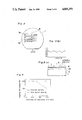
- FIG. 2 is a view for illustrating the formation direction, i.e. crystal growth direction, of the stripe-shaped thin film upon the application of the method of the present invention.
- FIGS. 3(a) and 3(b) show a principle chart for illustrating a method of controlling the reflection factor to provide a given temperature distribution to be employed in the method of the present invention
- FIG. 4 is a chart showing the influence of the size of the insulating-film exposed portion with regard to the seeding efficiency in the method of the present invention
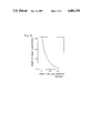
- FIG. 5 is a chart showing the relationship between the laser scanning direction and the length of a single crystal wherein the monocrystalline region is enlarged from the seed portion as in the method of the present invention.
- FIGS. 6(a) and 6(b) show views for illustrating the molten condition between the dot shape and the stripe shaped used in an insulating-film based on the employment of a conventional method.
- an insulating film 2 of non-crystalline material is formed on a top plane of a (100) monocrsytalline silicon base-plate 1 which is partially exposed to provide an exposed portion 1a, as shown in FIG. 1(b), of the monocrystalline silicon base-plate 1, as shown in FIG. 1(a).
- the size of the monocrystalline silicon base-plate exposed portion is assumed to be 3 ⁇ m square.
- a SiO 2 film of 2 ⁇ m in thickness is first formed on the monocrystalline silicon base-plate 1 by means of, for example, a known thermal oxidation method.
- the monocrystalline silicon base-plate 1 of the SiO 2 film is selectively etched by a known photo-etching method only at the portion to be exposed to form a plurality of exposed portions 1a, 1a, 1a, etc., having dot shapes, and each being 3 ⁇ m square at intervals of 15 ⁇ m, as shown in FIG. 2.
- non-crystalline or polycrystalline silicon thin film 3 which is almost equal in thickness to the insulating film 2, as shown in FIG. 1(c), is embedded only in the exposed portion 1a of the monocrystalline silicon base-plate 1 provided in and surrounded by the insulating film 2.
- either non-crystalline silicone thin-film or polycrystalline silicon thin-film is formed by a known LPCVD method on the whole surface of the insulating film 2 including the exposed portion 1a.
- organic application film material is applied by painting so as to evenly cover the whole surface of the non-crystalline or polycrystalline silicon thin-film, which is formed unevenly on the surface corresponding to the exposed portion 1a of the monocrystalline silicone base-plate 1 and the surface of the insulating film 2, to form an organic application film.
- the difference in surface thickness between the non-crystalline or polycrystalline silicon thin film 3 which is filled in at this time, and the insulating film 2 is assumed to be 1 ⁇ m or less.
- a non-crystalline or polycrystalline silicon thin film 4 which becomes an active layer of 0.6 ⁇ m in thickness is formed by the LPCVD method on both the upper filled portion of the thin film 3 and the upper portion of the insulating film 2, as shown in FIG. 1(d). Furthermore, an SiO 2 film which serves as a surface protective film, i.e. anti-reflective film 5, for the silicon thin film 4 is formed by the APCVD method, this SiO 2 film being 850 ⁇ in thickness over the whole surface of the silicon thin film 4, as shown in FIG. 1(e).
- laser beams 6 to 60 ⁇ m in molten width and 10 W in power are applied to the region including the monocrystalline silicon base-plate filled portion 1a, as shown in FIG. 1(f), and the non-crystalline or polycrystalline thin-film 4 on the monocrystalline silicon base-plate exposed portion 1a is caused to mono-crystallize with the monocrystalline silicon base-plate exposed portion 1a which is used as a seed for mono-crystallization, so that a monocrystalline thin-film 7 is obtained having a crystal direction coinciding with that of the monocrystalline silicon base-plate 1.
- a non-crystalline or polycrystalline silicon thin-film 8 having a stripe shape is formed on the surface of the surface protective film 5, as shown in FIGS. 1(g) and 1(h) in a longitudinal direction of the stripe so as to become (010) with respect to the monocrystalline silicon base plate 1, as shown in FIG. 2.
- the non-crystalline or polycrystalline silicon thin film 8 is formed 0.6 ⁇ m in thickness by using the LPCVD method on the surface protective film 5, and is made stripe-shaped through selective etching operation by a known photo-etching method.
- each stripe of the non-crystalline or polycrystalline silicon thin film 8 is formed to cover the monocrystalline silicon base-plate exposed portion 1a with a stripe width of 10 ⁇ m, the interval between the stripes being 5 ⁇ m.
- the scanning operation of the laser beam 9 of 60 ⁇ m in molten width and 12 W in power is conducted on the monocrystalline silicon base-plate exposed portion 1a with a scanning speed of 100 mm per second in the longitudinal direction of the stripe-shaped non-crystalline or polycrystalline silicon thin-film 8, as showing FIG. 1(i), to provide a monocrystalline silicon thin film 10 in which the non-crystalline or polycrystalline silicon thin-film 4 is mono-crystallized with the filled silicon 7 coincided with the monocrystal silicon base-plate 1 in the crystal direction being provided as the seed.
- the monocrystalline silicon thin-film 10 coinciding (100) with the monocrystaline silicon base-plate 1 in the crystal direction is finally obtained on the surface of the insulating film 2.
- the reason why the stripe-shaped non-crystalline or polycrystalline silicon thin-film 8 is formed is that the reflection factor, i.e. the reflectivity of the laser beam 9, in the place where the stripe-shaped silicon is located is enlarged to be greater than that in the place where the strip-shaped silicon does not exist, as shown in FIG. 3(a), the solidification for monocrystallization starts from under the stripe-shaped silicon central portion with a temperature distribution being provided, as shown in FIG. 3(b), and the monocrystalline growth of the silicon thin film 10 is caused by the monocrystalline silicon base-plate exposed portion 1a used as the seed.
- the reflection factor i.e. the reflectivity of the laser beam 9
- the change of the seeding efficiency of the seed due to changes in the insulating film 2 thickness and the size of the insulating film exposed portion 1a is examined for comparison, with the result shown in FIG. 4.
- the opening of the exposed portion 1a is as large as 5 ⁇ m square
- the seeding efficiency is lowered if the insulating film 2 becomes as thick as 4 ⁇ m.
- the exposed portion 1a is 2 ⁇ m, 3 ⁇ m or 4 ⁇ m square
- the seeding efficiency is not seen to drop if the thickness of the insulating 2 film is made 4 ⁇ m in thickness.
- the exposed portion 1a will do well if it is made 4 ⁇ m square or less in size, because even the largest thickness between the respective active layers is about 4 ⁇ m.
- the reason why the crystal face of the (100) is used as the monocrystalline silicon base-plate 1, and the laser scanning direction is along the (010) is that it is most difficult for a crystal defect to form with the combination of (100) and (010), and the monocrystalline region may be smoothly enlarged from the seed portion.
- the length for which the monocrystalline region extends from the seed portion when the laser scanning direction is varied between (010) and (011) by the use of (100) monocrystalline silicon base plate 1 that is used as shown in FIG. 5. It is most desirable from FIG. 5 that the laser scanning in the (010) direction is used. To enlarge the (100) crystal to the (010) is best even in comparison with the case in which the other crystal face is used. Superior results are similarly provided even if the (100) crystal of the symmetrical face equivalent to the (100) crystal is enlarged in the equivalent direction ⁇ 100>.
- a superior monocrystalline silicon thin-film having a crystal direction coinciding with that of a monocrystalline silicon base plate is formed on an insulating film even if the insulating film is as thick as 4 ⁇ m.
- the thin-film is sufficiently covered between the active layers of a three-dimensional circuit element on the monocrystalline silicon base plate.
Landscapes
- Recrystallisation Techniques (AREA)
Applications Claiming Priority (6)
| Application Number | Priority Date | Filing Date | Title |
|---|---|---|---|
| JP28543885A JPS62145721A (ja) | 1985-12-20 | 1985-12-20 | 単結晶薄膜の製造方法 |
| JP60-285438 | 1985-12-20 | ||
| JP6855486A JPS62226621A (ja) | 1986-03-28 | 1986-03-28 | 単結晶シリコン薄膜形成方法 |
| JP61-68554 | 1986-03-28 | ||
| JP61-225900 | 1986-09-26 | ||
| JP22590086A JPS6381807A (ja) | 1986-09-26 | 1986-09-26 | 単結晶シリコン薄膜の製造方法 |
Publications (1)
| Publication Number | Publication Date |
|---|---|
| US4801351A true US4801351A (en) | 1989-01-31 |
Family
ID=27299781
Family Applications (1)
| Application Number | Title | Priority Date | Filing Date |
|---|---|---|---|
| US06/943,428 Expired - Lifetime US4801351A (en) | 1985-12-20 | 1986-12-19 | Method of manufacturing monocrystalline thin-film |
Country Status (3)
| Country | Link |
|---|---|
| US (1) | US4801351A (de) |
| EP (1) | EP0227076B1 (de) |
| DE (1) | DE3685732T2 (de) |
Cited By (3)
| Publication number | Priority date | Publication date | Assignee | Title |
|---|---|---|---|---|
| US4931323A (en) * | 1987-12-10 | 1990-06-05 | Texas Instruments Incorporated | Thick film copper conductor patterning by laser |
| US5397735A (en) * | 1988-12-09 | 1995-03-14 | Thomson-Csf | Process for hardening active electronic components against ionizing radiations, and hardened components of large dimensions |
| EP1158580A3 (de) * | 1993-10-29 | 2004-07-28 | Semiconductor Energy Laboratory Co., Ltd. | Verfahren zum Kristallisieren einer Siliziumschicht |
Families Citing this family (2)
| Publication number | Priority date | Publication date | Assignee | Title |
|---|---|---|---|---|
| DE3779672T2 (de) * | 1986-03-07 | 1993-01-28 | Iizuka Kozo | Verfahren zum herstellen einer monokristallinen halbleiterschicht. |
| JPS62206816A (ja) * | 1986-03-07 | 1987-09-11 | Agency Of Ind Science & Technol | 半導体結晶層の製造方法 |
Citations (9)
| Publication number | Priority date | Publication date | Assignee | Title |
|---|---|---|---|---|
| US4383883A (en) * | 1980-08-11 | 1983-05-17 | Tokyo Shibaura Denki Kabushiki Kaisha | Method for fabricating semiconductor device |
| US4448632A (en) * | 1981-05-25 | 1984-05-15 | Mitsubishi Denki Kabushiki Kaisha | Method of fabricating semiconductor devices |
| US4487639A (en) * | 1980-09-26 | 1984-12-11 | Texas Instruments Incorporated | Localized epitaxy for VLSI devices |
| US4555300A (en) * | 1984-02-21 | 1985-11-26 | North American Philips Corporation | Method for producing single crystal layers on insulators |
| US4565584A (en) * | 1982-01-29 | 1986-01-21 | Hitachi, Ltd. | Method of producing single crystal film utilizing a two-step heat treatment |
| US4565599A (en) * | 1981-12-21 | 1986-01-21 | Massachusetts Institute Of Technology | Graphoepitaxy by encapsulation |
| US4651407A (en) * | 1985-05-08 | 1987-03-24 | Gte Laboratories Incorporated | Method of fabricating a junction field effect transistor utilizing epitaxial overgrowth and vertical junction formation |
| US4651408A (en) * | 1984-01-05 | 1987-03-24 | Northern Telecom Limited | Fabrication of stacked MOS devices utilizing lateral seeding and a plurality of separate implants at different energies |
| US4678538A (en) * | 1985-04-19 | 1987-07-07 | Etat Francais Represente Par Le Minitre Des Ptt, Centre National D'etudes Des Telecommunications | Process for the production of an insulating support on an oriented monocrystalline silicon film with localized defects |
Family Cites Families (1)
| Publication number | Priority date | Publication date | Assignee | Title |
|---|---|---|---|---|
| JPS59108313A (ja) * | 1982-12-13 | 1984-06-22 | Mitsubishi Electric Corp | 半導体単結晶層の製造方法 |
-
1986
- 1986-12-19 DE DE8686117799T patent/DE3685732T2/de not_active Expired - Fee Related
- 1986-12-19 US US06/943,428 patent/US4801351A/en not_active Expired - Lifetime
- 1986-12-19 EP EP86117799A patent/EP0227076B1/de not_active Expired - Lifetime
Patent Citations (9)
| Publication number | Priority date | Publication date | Assignee | Title |
|---|---|---|---|---|
| US4383883A (en) * | 1980-08-11 | 1983-05-17 | Tokyo Shibaura Denki Kabushiki Kaisha | Method for fabricating semiconductor device |
| US4487639A (en) * | 1980-09-26 | 1984-12-11 | Texas Instruments Incorporated | Localized epitaxy for VLSI devices |
| US4448632A (en) * | 1981-05-25 | 1984-05-15 | Mitsubishi Denki Kabushiki Kaisha | Method of fabricating semiconductor devices |
| US4565599A (en) * | 1981-12-21 | 1986-01-21 | Massachusetts Institute Of Technology | Graphoepitaxy by encapsulation |
| US4565584A (en) * | 1982-01-29 | 1986-01-21 | Hitachi, Ltd. | Method of producing single crystal film utilizing a two-step heat treatment |
| US4651408A (en) * | 1984-01-05 | 1987-03-24 | Northern Telecom Limited | Fabrication of stacked MOS devices utilizing lateral seeding and a plurality of separate implants at different energies |
| US4555300A (en) * | 1984-02-21 | 1985-11-26 | North American Philips Corporation | Method for producing single crystal layers on insulators |
| US4678538A (en) * | 1985-04-19 | 1987-07-07 | Etat Francais Represente Par Le Minitre Des Ptt, Centre National D'etudes Des Telecommunications | Process for the production of an insulating support on an oriented monocrystalline silicon film with localized defects |
| US4651407A (en) * | 1985-05-08 | 1987-03-24 | Gte Laboratories Incorporated | Method of fabricating a junction field effect transistor utilizing epitaxial overgrowth and vertical junction formation |
Non-Patent Citations (3)
| Title |
|---|
| Jadus et al., IBM Technical Disclosure Bull., vol. 14 (7), Dec. 1971. * |
| Tamura et al., Jap. J. Appl. Physics, vol. 19, pp. L23 26, (1980). * |
| Tamura et al., Jap. J. Appl. Physics, vol. 19, pp. L23-26, (1980). |
Cited By (7)
| Publication number | Priority date | Publication date | Assignee | Title |
|---|---|---|---|---|
| US4931323A (en) * | 1987-12-10 | 1990-06-05 | Texas Instruments Incorporated | Thick film copper conductor patterning by laser |
| US5397735A (en) * | 1988-12-09 | 1995-03-14 | Thomson-Csf | Process for hardening active electronic components against ionizing radiations, and hardened components of large dimensions |
| EP1158580A3 (de) * | 1993-10-29 | 2004-07-28 | Semiconductor Energy Laboratory Co., Ltd. | Verfahren zum Kristallisieren einer Siliziumschicht |
| US6998639B2 (en) | 1993-10-29 | 2006-02-14 | Semiconductor Energy Laboratory Co., Ltd. | Method for manufacturing a semiconductor device |
| US20060131583A1 (en) * | 1993-10-29 | 2006-06-22 | Semiconductor Energy Laboratory Co., Ltd. | Method for manufacturing a semiconductor device |
| US20090035923A1 (en) * | 1993-10-29 | 2009-02-05 | Semiconductor Energy Laboratory Co., Ltd. | Method for manufacturing a semiconductor device |
| US7998844B2 (en) | 1993-10-29 | 2011-08-16 | Semiconductor Energy Laboratory Co., Ltd. | Method for manufacturing a semiconductor device |
Also Published As
| Publication number | Publication date |
|---|---|
| EP0227076A2 (de) | 1987-07-01 |
| EP0227076B1 (de) | 1992-06-17 |
| DE3685732T2 (de) | 1993-01-21 |
| EP0227076A3 (en) | 1989-05-24 |
| DE3685732D1 (de) | 1992-07-23 |
Similar Documents
| Publication | Publication Date | Title |
|---|---|---|
| US4670088A (en) | Lateral epitaxial growth by seeded solidification | |
| US4576851A (en) | Semiconductor substrate | |
| EP0077020B1 (de) | Verfahren zur Herstellung einer monokristallinen Schicht | |
| US4371421A (en) | Lateral epitaxial growth by seeded solidification | |
| US5310446A (en) | Method for producing semiconductor film | |
| US4523962A (en) | Method for fabricating monocrystalline semiconductor layer on insulating layer by laser crystallization using a grid of anti-reflection coating disposed on poly/amorphous semiconductor | |
| JPS6076118A (ja) | 半導体デバイスの製作法 | |
| EP0236953B1 (de) | Herstellungsverfahren einer Halbleiter-Kristallschicht | |
| US4801351A (en) | Method of manufacturing monocrystalline thin-film | |
| WO1982003639A1 (en) | Lateral epitaxial growth by seeded solidification | |
| US4678538A (en) | Process for the production of an insulating support on an oriented monocrystalline silicon film with localized defects | |
| US5094714A (en) | Wafer structure for forming a semiconductor single crystal film | |
| EP0575965A2 (de) | Verfahren zur Herstellung eines Halbleiter-Kristals und Halbleiteranordnung | |
| GB2153253A (en) | Semiconductor device and process for making it | |
| WO1987003916A1 (en) | Method of forming single crystal silicon using spe seed and laser crystallization | |
| JPH0442358B2 (de) | ||
| JPS62179112A (ja) | Soi構造形成方法 | |
| Isu et al. | Topographical characteristics of recrystallized silicon films by scanning cw laser irradiation | |
| JPH04214615A (ja) | 半導体デバイスの製造方法 | |
| JPS62145721A (ja) | 単結晶薄膜の製造方法 | |
| JPS6167218A (ja) | 半導体装置の製造方法 | |
| JPH0519976B2 (de) | ||
| JPS6246510A (ja) | 半導体装置の製造方法 | |
| JPH0153509B2 (de) | ||
| JPH0149003B2 (de) |
Legal Events
| Date | Code | Title | Description |
|---|---|---|---|
| AS | Assignment |
Owner name: AGENCY OF INDUSTRIAL SCIENCE AND TECHNOLOGY, AN EX Free format text: ASSIGNMENT OF ASSIGNORS INTEREST.;ASSIGNORS:AWANE, KATUNOBU;KOBA, MASAYOSHI;MIYAJIMA, TOSHIAKI;AND OTHERS;REEL/FRAME:004650/0443 Effective date: 19861210 Owner name: AGENCY OF INDUSTRIAL SCIENCE AND TECHNOLOGY, AN EX Free format text: ASSIGNMENT OF ASSIGNORS INTEREST;ASSIGNORS:AWANE, KATUNOBU;KOBA, MASAYOSHI;MIYAJIMA, TOSHIAKI;AND OTHERS;REEL/FRAME:004650/0443 Effective date: 19861210 |
|
| STCF | Information on status: patent grant |
Free format text: PATENTED CASE |
|
| FEPP | Fee payment procedure |
Free format text: PAYOR NUMBER ASSIGNED (ORIGINAL EVENT CODE: ASPN); ENTITY STATUS OF PATENT OWNER: LARGE ENTITY |
|
| FPAY | Fee payment |
Year of fee payment: 4 |
|
| FEPP | Fee payment procedure |
Free format text: PAYER NUMBER DE-ASSIGNED (ORIGINAL EVENT CODE: RMPN); ENTITY STATUS OF PATENT OWNER: LARGE ENTITY Free format text: PAYOR NUMBER ASSIGNED (ORIGINAL EVENT CODE: ASPN); ENTITY STATUS OF PATENT OWNER: LARGE ENTITY |
|
| FPAY | Fee payment |
Year of fee payment: 8 |
|
| FPAY | Fee payment |
Year of fee payment: 12 |