US4740995A - Variable frequency sinusoidal signal generator, in particular for a modem - Google Patents
Variable frequency sinusoidal signal generator, in particular for a modem Download PDFInfo
- Publication number
- US4740995A US4740995A US07/056,342 US5634287A US4740995A US 4740995 A US4740995 A US 4740995A US 5634287 A US5634287 A US 5634287A US 4740995 A US4740995 A US 4740995A
- Authority
- US
- United States
- Prior art keywords
- signal
- sinusoidal
- frequency
- signal generator
- signals
- Prior art date
- Legal status (The legal status is an assumption and is not a legal conclusion. Google has not performed a legal analysis and makes no representation as to the accuracy of the status listed.)
- Expired - Lifetime
Links
Images


Classifications
-
- H—ELECTRICITY
- H03—ELECTRONIC CIRCUITRY
- H03K—PULSE TECHNIQUE
- H03K4/00—Generating pulses having essentially a finite slope or stepped portions
- H03K4/02—Generating pulses having essentially a finite slope or stepped portions having stepped portions, e.g. staircase waveform
- H03K4/026—Generating pulses having essentially a finite slope or stepped portions having stepped portions, e.g. staircase waveform using digital techniques
-
- H—ELECTRICITY
- H04—ELECTRIC COMMUNICATION TECHNIQUE
- H04L—TRANSMISSION OF DIGITAL INFORMATION, e.g. TELEGRAPHIC COMMUNICATION
- H04L27/00—Modulated-carrier systems
- H04L27/10—Frequency-modulated carrier systems, i.e. using frequency-shift keying
- H04L27/12—Modulator circuits; Transmitter circuits
- H04L27/122—Modulator circuits; Transmitter circuits using digital generation of carrier signals
Definitions
- This invention relates to the modulation of a sinusoidal type signal by a binary signal. More specifically, it relates to a sinusoidal signal generator whose frequency is dependent upon a binary signal to be transmitted.
- the invention finds particularly advantageous application in modulators/demodulators or modems adapted for transmitting binary signals on a telephone line.
- the memory contains a certain number of binary values which are addressed by the data to be transmitted and when they are selected produce in the convertor a sample level which represents the sinusoidal signal.
- Such an arrangement has the drawback of being complex and the output signal is impaired by a quantification noise such that the sinusoidal signal obtained does not accurately reflect the input binary data.
- the invention contemplates therefore firstly the provision of a sinusoidal wave generator the frequency of which is dependent upon a binary signal, and which will be generated with minimal distortion and with a good phase coherence.
- the invention also contemplates providing a telephone modem including a generator of the type indicated, permitting the possibility of realizing an entire integrated circuit on a single semiconductor chip.
- the invention provides a generator of the type indicated above including a clock generator programmable as a function of the binary signal and adapted to produce at least two clock signals of different frequencies, a digital/analog convertor which, as a function of the clock signals used as sampling signals, generates, from a fixed voltage difference, a step signal having a sinusoidal envelope whose fundamental frequency is a function of one or the other of said clock signals, and a low pass filter whose transfer function is dependent upon the selection of the clock signals for rejecting the harmonics contained in the step signal produced by said convertor, the filter providing at the output the sinusoidal signal representing said binary signal.
- a clock generator programmable as a function of the binary signal and adapted to produce at least two clock signals of different frequencies
- a digital/analog convertor which, as a function of the clock signals used as sampling signals, generates, from a fixed voltage difference, a step signal having a sinusoidal envelope whose fundamental frequency is a function of one or the other of said clock signals, and a low pass filter
- CMOS complementary metal-oxide-semiconductor
- sinusoid produced is harmonic filtered so that one can avoid the difficulties created by harmonic distortions and group delay.
- the invention also provides a telephone modem having a generator such as set forth above.
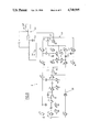
- FIG. 1 is a very simplified diagram of a controlled sinisoidal wave generator, embodying the invention.
- FIG. 2 is a diagram of the sinusoidal wave form obtained in the D/A convertor.
- FIG. 3 is a simplified diagram of the convertor.
- FIG. 4 shows the frequency spectrum of the wave form generated in the convertor.
- FIG. 5 is a detailed diagram of the D/A convertor.
- FIGS. 6 and 7 represent the signals appearing in the convertor.
- FIG. 8 is a diagram of the controlled filter connected to the convertor of FIG. 5.
- FIG. 9 is a diagram equivalent to the first section of the filter.
- FIGS. 10 and 11 are the wave form and the spectrum, respectively, of the output signal of the first section of the filter.
- FIG. 12 is an equivalent diagram of the second section of the filter.
- FIGS. 13 and 14 are the wave form and the spectrum, respectively, of the output signal and the spectrum of the second section of the filter.
- FIG. 15 is a gain/frequency and phase/frequency illustrating the performance of an embodiment of the invention.
- FIG. 1 shows a very simplified diagram of a sinusoidal wave generator embodying the invention.
- This generator includes a stable base clock 1 providing a very high frequency signal of about 4 MHZ for example.
- the frequency output of this clock is divided into several control signals in frequency divider 2 the division ratio of which is programmable as a function of one or more signals which are applied on leads 3, 4, and 5.
- the lead 3 can receive for example a binary signal, the levels of which can alternatively select two frequencies at the output of the divider while the leads 4 and 5 are adapted to selectively determine the different frequency pairs from which each of the frequencies is selected in the manner indicated by lead 3.
- the frequency divider 2 is constructed.
- This latter provides on its outputs control signals, the frequency of which reflect the state of the inputs 3, 4, and 5.
- the leads 4 and 5 can be placed at a high or low level so that four combinations of two frequencies can be selected.
- the generator thus conceived is particularly well adapted to be incorporated into a multistandard modem, the lead 3 receiving the binary signals to be transmitted and the leads 4 and 5 receiving a binary signal, the value representing one of the selected standards indicated above in Table 1.
- a group of variable frequency control signals is applied by line 6 to a digital-to-analog (D/A) convertor 7 connected to reference source 8, while the wave form obtained by sampling at the output of the convertor is applied by line 9 to a low-pass filter 10, the transfer function of which can be modified as a function of the control signal from divider 2 over line 11, this transfer function depending on the signals applied over leads 3 to 5.
- Output 12 of filter 10 transmits a sinusoidal signal, the frequency of which is controlled by the logical state of the leads 3 to 5.
- the construction of the generator to be described is based on the fact that one can generate a sinusoidal envelope voltage from the absolute value of two levels of reference voltage by sampling these levels selectively at a rate which is eight times the frequency of the sinusoid to be obtained.
- FIG. 2 shows the envelope of the sinusoidal wave form obtained from said levels, having respectively a positive or negative sign. It is seen that two consecutive samples are generated at an interval corresponding to a phase angle of pi/4.
- the voltage levels have a relation with the form ##EQU1## which can be obtained with respect to two appropriate impedances connected to a reference voltage fixed to the rate of the sampling and in assigning the correct sign to each sample.
- the principle allowing for sampling this signal in this manner is ()* in FIG. 3.
- the impedences utilized are preferably capacitors easily made with CMOS technology.
- the precision of the voltage samplings depends upon a relation of the capacitors such that the envelope of the wave form to be generated can very closely approach a sinusoid.
- a sinusoidal signal produced in this manner has, other than its fundamental frequency, as first important harmonics, only the seventh and ninth harmonics as well as other odd harmonics according to the frequency spectrum of FIG. 4.
- the diagram shows at the ordinate the relative energy between the fundamental and the harmonics and at the abscissa the numbers of the harmonics of the spectrum. It will be seen subsequently that such a spectrum can be conveniently filtered by a filter, the transfer function of which is dependent upon the fundamental frequency of the sinusoidal envelope signal, a frequency which is in fact representative of the binary signal, upon which the frequency of the sinusoid is itself dependent.
- FIG. 3 shows an operational amplifier 13, the non-inverting input of which is permanently connected to ground or to a potential fixed relative to another value.
- the inverting input is connected to junction 14 to which is connected three capacitors C1, C2, and C3.
- the capacitor C3 is connected between the inverting input and the output of amplifier 13.
- Holding capacitor C4 is connected between the output of this latter and the voltage Vss.
- the capacitors to C4 can be switched in or out of circuit or connected to voltages Vr and Vss by means CMOS transistor switches i-a to i-f indicated in FIG. 3 by small circles and controlled selectively by cyclic signals. The nature and the form of these signals will be set forth hereinafter with the detailed description of the convertor.
- the letters and b are assigned to the capacitors C1 to C3.
- the values of the capacitors C1 to C3 are not the same and they are selected to provide the absolute values of the voltages V1 and V2 of FIG. 2 or, in other words, the positive or negative height of the steps or samples of the desired signal.
- each step is generated by repeating a certain number of times (16 in the example), an elementary functioning cycle which itself has two stages.
- the first stage neutralizes the charges of the preceding elementary cycle on the capacitors which were just used
- the second stage called “redistribution” creates on the holding capacitor C4, the voltage V1 or V2 with the assistance of either the capacitors C1 and C3 or capacitors C2 and C3.
- Each elementary signal is controlled by the proper opening of switches i-a to i-e which causes the switching of the capacitors to the differences of the distinct voltages Vr and Vss.
- the capacitor C4 thus receives a voltage which corresponds to a proportion of the difference in voltage between Vr and Vss, this proportion being a function of the relation between the values of the capacitors C1 and C3 on the one hand and C2 and C3 on the other.
- Table 2 gives the state of the charge of the capacitors C1 to C4 for producing the steps 1 to 8 of FIG. 2, the first line of the table corresponding to the start of the function.
- FIGS. 5, 6 and 7 which relate to a practical convertor arrangement will now be described
- FIG. 5 shows four capacitors C1 to C4 and an operational amplifier 13 whose inverting input is connected to junction point 14. Voltages Vss and Vr are applied respectively to lines 15 and 16. These voltages are selectively transmitted to capacitors C1, C2, and C3 by the groups of CMOS transistors whose control electrodes receive signals derived from the signals applied to frequency divider 2.
- FIGS. 6 and 7 as well as the right portion of table II show the transistor control sequence, it being understood that the scales of FIGS. 6 and 7 are different.
- the capacitors C1 and C2 are each connected, by several transistors whose role is secondary and not described here, to four voltage application circuits connected by pair of lines 15 and 16 respectively.
- Each of these circuits include two transistors having references 17a to 24a and 17b to 24b which are selectively controlled, in regard to capacitor C1, by signals QX, NOX, K1 and K2 and, in regard to capacitor C2, by signals G2X, NG2X, K1 and K2P.
- the phase ratios and the logical levels of the signals are clearly seen in FIGS. 6 and 7.
- the control signals are generated from the output signals of the frequency divider and applied to the corresponding transistors via delay and shaping circuits 25, 26, and 27.
- frequency divider 2 functions from a very precise base frequency and operates on, for each state "1" or "0" of input 3, a group of signals whose frequencies have fixed relations among themselves.
- designating the base frequency as FB one obtains:
- F determines according to its high or low level which of the capacitors C1 and C2 is utilized, while G determines the polarity of the sine to be generated, that is, a positive polarity when G is at zero and vice-versa.
- the frequency FB is determined on the one hand by the state of the input 3 and on the other hand by the standard selection signal applied to outputs 4 and 5 and a change of state on one of these imputs immediately causes a change of all of the transistor control frequencies, with the conservation of the ratios indicated above.
- FIG. 8 the filter 10 which provides for the elimination of the upper harmonics from the frequency spectrum of the sinusoidal signal generated by generator 7, the energy content of which, in relation to that of the fundamental frequency, is seen in FIG. 4.
- FIG. 8 shows a detailed schematic of filter 10 which has three active filtering sections 28, 29 and 30 and which has a low pass attenuation curve.
- the first section 28 is a second order cell, the equivalent schematic of which is seen in FIG. 9. Its input 31 is connected to the output of generator 7 D/A converter 7 (FIG. 5), and its transfer function is determined by the capacitor network which is placed in and out of circuit under control of CMOS switches, the control electrodes of which selectively receive the signals K1 and K2 from frequency divider 2.
- the equivalent functions of the switched capacitors are symbolized by variable resistors 32, 33, 34, and 35. It is to be noted that the signal K2 controls the precharge of the capacitors while the signal K2 determines the redistribution of the charges on the capactors.
- the attenuation central frequency of the filter section 28 is fixed at eight times the fundamental frequency so that it attenuates all of the harmonics of generator 2 except the harmonics which are a multiple between plus and minus 1 of the control frequency of the transistors of the section.
- the spectrum of the output signal of section 28 shows several energy crests located at the fundamental frequency and at harmonics 63, 65, 127, 129 etc., all of the other harmonics being considerably surpressed.
- FIG. 10 shows the sinusoidal signal having the form of a stair having 64 levels per period, each level corresponding to a precharge operation and an operation of redistribution of the capacitors of the filtering section.
- filter section 29 which is of the first order and which assures a binary transforation, the property of which is to generate a "transmission zero" at half of the sampling frequency. Its equivalent schematic is seen in FIG. 12.
- This equivalent schematic shows that this section has an operational amplifier 37 associated with integrating capacitor 38 and an equivalent resistance 39.
- One of the inputs of the amplifier is connected to the output 36 by an equivalent resistance 40.
- This equivalent arrangement is in fact formed (FIG. 8) by two distinct parts of this section, of which amplifier 37 and capacitor 38 constitute known components.
- the equivalent resistance 39, 40 are formed by four capacitors in the real circuit of FIG. 8, namely, capacitors 42 and 45 which are selectively placed in circuit by the control transistors directed by the signals K1 and K2 such that at all times the parts of the section constitute, with the amplifier 37 and the capacitor 38, the filter section of the first order.
- the signals K1 and K2 are out of phase by 180° and each has a frequency which is equal to 64 times the fundamental frequency Ff, the filter generates 128 samples per period of the fundamental sinusoid and this alternatively by the two parts of the section.
- the sinusoidal signal appearing at the output 46 of section 29 has the shape of the curve of FIG. 13 in which there is seen a period of the signal including 128 steps.
- This output 46 is connected to the third active filter section 30 (FIG. 8) whose configurations appears as a Bessel filter. This configuration is fixed and does not depend on control signals K1 and K2.
- the filter section is of the third order and assures the attenuation of the remaining harmonics (128th and multiples) of the fundamental frequency so that the sinusoidal signal undergoes a simple smoothing.
- the output lead 47 of section 30 is connected to an emitter device 48 which feeds the telephonic transmission line.
- FIG. 15 shows a diagram representing the results obtained with an embodiment according to the invention as put into practice.
- the verticals A and B correspond to two transmission frequencies F1 and F2 of the binary signal at the one and zero levels. It is seen that the gain and phase are practically not changed when the useful signal goes between the two logical levels.
- the filter 10 which has been described thus transforms the output signal of the generator 2 to a sinusoidal signal of very low distortion while maintaining at a reduced level the group propagation time and the amplitude distortion for the two levels of the binary signal to be transmitted.
- phase coherence at the times when the binary signal to be transmitted has transitions is maximized as the passage from one frequency to another is effected immediately, that is, within the period of control signals K1 to K2, which have a frequency which is equal to 128 times the fundamental frequency, depending on whether the binary signal is 1 or 0.
- the maximum positioning error (distortion isochrome) of a transition of this signal is equal to the duration of the largest segment of the output signal of generator 1. To transmit a signal at 1200 Bauds, this error is 6.54s which is an error of 0.8%.
Applications Claiming Priority (2)
| Application Number | Priority Date | Filing Date | Title |
|---|---|---|---|
| FR8313669A FR2551279B1 (fr) | 1983-08-24 | 1983-08-24 | Generateur d'onde sinusoidale, dont la frequence est asservie a un signal binaire, notamment pour modem |
| FR8313669 | 1983-08-24 |
Related Parent Applications (1)
| Application Number | Title | Priority Date | Filing Date |
|---|---|---|---|
| US06642271 Continuation | 1984-08-20 |
Publications (1)
| Publication Number | Publication Date |
|---|---|
| US4740995A true US4740995A (en) | 1988-04-26 |
Family
ID=9291784
Family Applications (1)
| Application Number | Title | Priority Date | Filing Date |
|---|---|---|---|
| US07/056,342 Expired - Lifetime US4740995A (en) | 1983-08-24 | 1987-05-27 | Variable frequency sinusoidal signal generator, in particular for a modem |
Country Status (5)
| Country | Link |
|---|---|
| US (1) | US4740995A (fr) |
| EP (1) | EP0135437B1 (fr) |
| JP (1) | JPS6074803A (fr) |
| DE (1) | DE3475154D1 (fr) |
| FR (1) | FR2551279B1 (fr) |
Cited By (9)
| Publication number | Priority date | Publication date | Assignee | Title |
|---|---|---|---|---|
| US4823090A (en) * | 1987-10-02 | 1989-04-18 | Tektronix, Inc. | Digital signal synthesis using low frequency sampling clock |
| US4926131A (en) * | 1987-06-25 | 1990-05-15 | Schlumberger Industries, Inc. | Triangle waveform generator for pulse-width amplitude multiplier |
| US5014285A (en) * | 1989-09-27 | 1991-05-07 | General Electric Company | Frequency shift keying communication system with selectable carrier frequencies |
| US5070254A (en) * | 1989-03-17 | 1991-12-03 | U.S. Philips Corporation | Pulse generators with constant mark/space ratio and small phase modulation jitter |
| US5162745A (en) * | 1990-01-31 | 1992-11-10 | U.S. Philips Corporation | Multichannel sine synthesizer |
| US6320431B1 (en) | 1999-10-08 | 2001-11-20 | National Semiconductor Corporation | Apparatus and method of generating numerically controlled oscillator signals |
| US20050270193A1 (en) * | 2004-05-18 | 2005-12-08 | Victor Dias | Method and device for reducing the signal images at the output of a digital/analogue converter |
| US7349488B1 (en) * | 2003-04-10 | 2008-03-25 | Xilinx, Inc. | Frequency shift keying signaling for integrated circuits |
| US20110187421A1 (en) * | 2008-08-07 | 2011-08-04 | Nxp B.V. | Signal generation method and apparatus and test method and system using the same |
Families Citing this family (4)
| Publication number | Priority date | Publication date | Assignee | Title |
|---|---|---|---|---|
| JP2621346B2 (ja) * | 1988-05-23 | 1997-06-18 | 松下電器産業株式会社 | 映像信号処理回路 |
| US5039872A (en) * | 1989-09-28 | 1991-08-13 | The United States Of America As Represented By The Secretary Of Commerce | Digitally synthesized audio frequency voltage source |
| US5189381A (en) * | 1991-10-31 | 1993-02-23 | Advanced Micro Devices, Inc. | Apparatus for generating a sinusoidal output signal |
| NZ562739A (en) * | 2007-10-19 | 2010-04-30 | Waikatolink Ltd | Signal simulation apparatus and method |
Citations (9)
| Publication number | Priority date | Publication date | Assignee | Title |
|---|---|---|---|---|
| US3668562A (en) * | 1970-04-15 | 1972-06-06 | Tel Tech Corp | Frequency modulation system for transmitting binary information |
| US3740669A (en) * | 1971-11-01 | 1973-06-19 | Rca Corp | M-ary fsk digital modulator |
| US3792360A (en) * | 1972-08-14 | 1974-02-12 | Motorola Inc | Multi-frequency signal generator |
| US4171466A (en) * | 1977-05-16 | 1979-10-16 | Bell Telephone Laboratories, Incorporated | Digital wave generator for composite tone |
| EP0016281A1 (fr) * | 1979-03-14 | 1980-10-01 | Teltone Corporation | Système numérique à porteuse, en particulier système numérique à porteuse abonné/numérique et synthétiseur de fréquence adapté à cette fin |
| US4328554A (en) * | 1980-07-03 | 1982-05-04 | The United States Of America As Represented By The Secretary Of The Navy | Programmable frequency synthesizer (PFS) |
| US4368432A (en) * | 1980-11-12 | 1983-01-11 | Siemens Corporation | Sine wave generator for different frequencies |
| EP0075161A1 (fr) * | 1981-09-22 | 1983-03-30 | Racal Data Communications, Inc. | Modulateur à capacité commutée |
| US4486846A (en) * | 1982-06-28 | 1984-12-04 | Motorola Inc. | Numerically controlled oscillator using quadrant replication and function decomposition |
Family Cites Families (3)
| Publication number | Priority date | Publication date | Assignee | Title |
|---|---|---|---|---|
| FR2336831A1 (fr) * | 1975-12-24 | 1977-07-22 | Texas Instruments France | Generateur de signaux a basse frequence, notamment de signaux de tonalite |
| US4142245A (en) * | 1977-08-22 | 1979-02-27 | Texas Instruments Incorporated | Multi-frequency digital wave synthesizer for providing analog output signals |
| US4468749A (en) * | 1980-08-20 | 1984-08-28 | Fujitsu Limited | Adjustable attenuator circuit |
-
1983
- 1983-08-24 FR FR8313669A patent/FR2551279B1/fr not_active Expired
-
1984
- 1984-08-22 EP EP84401705A patent/EP0135437B1/fr not_active Expired
- 1984-08-22 DE DE8484401705T patent/DE3475154D1/de not_active Expired
- 1984-08-24 JP JP59176512A patent/JPS6074803A/ja active Pending
-
1987
- 1987-05-27 US US07/056,342 patent/US4740995A/en not_active Expired - Lifetime
Patent Citations (9)
| Publication number | Priority date | Publication date | Assignee | Title |
|---|---|---|---|---|
| US3668562A (en) * | 1970-04-15 | 1972-06-06 | Tel Tech Corp | Frequency modulation system for transmitting binary information |
| US3740669A (en) * | 1971-11-01 | 1973-06-19 | Rca Corp | M-ary fsk digital modulator |
| US3792360A (en) * | 1972-08-14 | 1974-02-12 | Motorola Inc | Multi-frequency signal generator |
| US4171466A (en) * | 1977-05-16 | 1979-10-16 | Bell Telephone Laboratories, Incorporated | Digital wave generator for composite tone |
| EP0016281A1 (fr) * | 1979-03-14 | 1980-10-01 | Teltone Corporation | Système numérique à porteuse, en particulier système numérique à porteuse abonné/numérique et synthétiseur de fréquence adapté à cette fin |
| US4328554A (en) * | 1980-07-03 | 1982-05-04 | The United States Of America As Represented By The Secretary Of The Navy | Programmable frequency synthesizer (PFS) |
| US4368432A (en) * | 1980-11-12 | 1983-01-11 | Siemens Corporation | Sine wave generator for different frequencies |
| EP0075161A1 (fr) * | 1981-09-22 | 1983-03-30 | Racal Data Communications, Inc. | Modulateur à capacité commutée |
| US4486846A (en) * | 1982-06-28 | 1984-12-04 | Motorola Inc. | Numerically controlled oscillator using quadrant replication and function decomposition |
Non-Patent Citations (2)
| Title |
|---|
| Elektronik, vol. 30, No. 16, Aug. 1981, pp. 64 66, Munich, De; M. Arnoldt * |
| Elektronik, vol. 30, No. 16, Aug. 1981, pp. 64-66, Munich, De; M. Arnoldt |
Cited By (11)
| Publication number | Priority date | Publication date | Assignee | Title |
|---|---|---|---|---|
| US4926131A (en) * | 1987-06-25 | 1990-05-15 | Schlumberger Industries, Inc. | Triangle waveform generator for pulse-width amplitude multiplier |
| US4823090A (en) * | 1987-10-02 | 1989-04-18 | Tektronix, Inc. | Digital signal synthesis using low frequency sampling clock |
| US5070254A (en) * | 1989-03-17 | 1991-12-03 | U.S. Philips Corporation | Pulse generators with constant mark/space ratio and small phase modulation jitter |
| US5014285A (en) * | 1989-09-27 | 1991-05-07 | General Electric Company | Frequency shift keying communication system with selectable carrier frequencies |
| US5162745A (en) * | 1990-01-31 | 1992-11-10 | U.S. Philips Corporation | Multichannel sine synthesizer |
| US6320431B1 (en) | 1999-10-08 | 2001-11-20 | National Semiconductor Corporation | Apparatus and method of generating numerically controlled oscillator signals |
| US7349488B1 (en) * | 2003-04-10 | 2008-03-25 | Xilinx, Inc. | Frequency shift keying signaling for integrated circuits |
| US20050270193A1 (en) * | 2004-05-18 | 2005-12-08 | Victor Dias | Method and device for reducing the signal images at the output of a digital/analogue converter |
| US7280061B2 (en) * | 2004-05-18 | 2007-10-09 | Infineon Technologies Ag | Digital-to-analog converter using a frequency hopping clock generator |
| US20110187421A1 (en) * | 2008-08-07 | 2011-08-04 | Nxp B.V. | Signal generation method and apparatus and test method and system using the same |
| US8497792B2 (en) | 2008-08-07 | 2013-07-30 | Nxp B.V. | Signal generation method and apparatus and test method and system using the same |
Also Published As
| Publication number | Publication date |
|---|---|
| JPS6074803A (ja) | 1985-04-27 |
| EP0135437B1 (fr) | 1988-11-09 |
| FR2551279B1 (fr) | 1988-10-14 |
| EP0135437A1 (fr) | 1985-03-27 |
| FR2551279A1 (fr) | 1985-03-01 |
| DE3475154D1 (en) | 1988-12-15 |
Similar Documents
| Publication | Publication Date | Title |
|---|---|---|
| US4740995A (en) | Variable frequency sinusoidal signal generator, in particular for a modem | |
| US3500213A (en) | Sinewave synthesizer for telegraph systems | |
| Martin et al. | Switched-capacitor building blocks for adaptive systems | |
| US3500215A (en) | Filter for bivalent pulse signals | |
| DE69928934T2 (de) | Verfahren und gerät zur korrektur des gleichspannungsversatzes in digital-analog-wandlern | |
| US3868601A (en) | Digital single-sideband modulator | |
| US5331218A (en) | Switched-capacitor notch filter with programmable notch width and depth | |
| US3962549A (en) | Threshold detector circuitry, as for PCM repeaters | |
| EP0686323B1 (fr) | Convertisseurs analogiques-numeriques et convertisseurs numeriques-analogiques a un bit utilisant un filtre adaptatif a deux regimes de fonctionnement | |
| US3778722A (en) | Receiver for data signals, including an automatic line correction circuit | |
| US4127846A (en) | Tone signal detecting circuit | |
| EP0258432A1 (fr) | Generateur de bruit multimode a modulation de frequence numerique. | |
| US3314062A (en) | Analog-to-digital converter | |
| CA1233890A (fr) | Filtre decimateur | |
| US3824413A (en) | Analog feedback frequency responsive circuit | |
| US4455539A (en) | Switched capacitor all pass filter | |
| JPS6145409B2 (fr) | ||
| US5461583A (en) | Programmable frequency sine wave signal generator | |
| US4358737A (en) | Digitally controlled bandwidth sampling filter-detector | |
| US3745473A (en) | Mixer circuit | |
| US3968354A (en) | Transversal digital filter for delta coded signals | |
| US5500613A (en) | Method for producing a digital sine wave signal with a given sampling rate, and circuit configuration for carrying out the method | |
| US3388219A (en) | Active filters for electrical signalling systems | |
| SU1109933A1 (ru) | Частотный манипул тор | |
| US3139537A (en) | Low frequency square wave to sine wave shaper |
Legal Events
| Date | Code | Title | Description |
|---|---|---|---|
| STCF | Information on status: patent grant |
Free format text: PATENTED CASE |
|
| FPAY | Fee payment |
Year of fee payment: 4 |
|
| FEPP | Fee payment procedure |
Free format text: PAYOR NUMBER ASSIGNED (ORIGINAL EVENT CODE: ASPN); ENTITY STATUS OF PATENT OWNER: LARGE ENTITY |
|
| FPAY | Fee payment |
Year of fee payment: 8 |
|
| FPAY | Fee payment |
Year of fee payment: 12 |