US4642412A - Photo-electronic conversion apparatus with light pattern discriminator - Google Patents
Photo-electronic conversion apparatus with light pattern discriminator Download PDFInfo
- Publication number
- US4642412A US4642412A US06/759,961 US75996185A US4642412A US 4642412 A US4642412 A US 4642412A US 75996185 A US75996185 A US 75996185A US 4642412 A US4642412 A US 4642412A
- Authority
- US
- United States
- Prior art keywords
- photo
- photovoltaic devices
- conversion apparatus
- electric
- electric conversion
- Prior art date
- Legal status (The legal status is an assumption and is not a legal conclusion. Google has not performed a legal analysis and makes no representation as to the accuracy of the status listed.)
- Expired - Fee Related
Links
- 238000006243 chemical reaction Methods 0.000 title claims abstract description 22
- 239000000758 substrate Substances 0.000 claims description 3
- 229910021417 amorphous silicon Inorganic materials 0.000 description 2
- 229910001218 Gallium arsenide Inorganic materials 0.000 description 1
- 238000010276 construction Methods 0.000 description 1
- 230000007547 defect Effects 0.000 description 1
- 238000001514 detection method Methods 0.000 description 1
- 230000005611 electricity Effects 0.000 description 1
- 239000010408 film Substances 0.000 description 1
- 239000011521 glass Substances 0.000 description 1
- 230000001678 irradiating effect Effects 0.000 description 1
- 239000004065 semiconductor Substances 0.000 description 1
- 239000010409 thin film Substances 0.000 description 1
Images

Classifications
-
- H—ELECTRICITY
- H10—SEMICONDUCTOR DEVICES; ELECTRIC SOLID-STATE DEVICES NOT OTHERWISE PROVIDED FOR
- H10F—INORGANIC SEMICONDUCTOR DEVICES SENSITIVE TO INFRARED RADIATION, LIGHT, ELECTROMAGNETIC RADIATION OF SHORTER WAVELENGTH OR CORPUSCULAR RADIATION
- H10F77/00—Constructional details of devices covered by this subclass
- H10F77/95—Circuit arrangements
- H10F77/953—Circuit arrangements for devices having potential barriers
- H10F77/957—Circuit arrangements for devices having potential barriers for position-sensitive photodetectors, e.g. lateral-effect photodiodes or quadrant photodiodes
-
- Y—GENERAL TAGGING OF NEW TECHNOLOGICAL DEVELOPMENTS; GENERAL TAGGING OF CROSS-SECTIONAL TECHNOLOGIES SPANNING OVER SEVERAL SECTIONS OF THE IPC; TECHNICAL SUBJECTS COVERED BY FORMER USPC CROSS-REFERENCE ART COLLECTIONS [XRACs] AND DIGESTS
- Y10—TECHNICAL SUBJECTS COVERED BY FORMER USPC
- Y10S—TECHNICAL SUBJECTS COVERED BY FORMER USPC CROSS-REFERENCE ART COLLECTIONS [XRACs] AND DIGESTS
- Y10S136/00—Batteries: thermoelectric and photoelectric
- Y10S136/291—Applications
Definitions
- This invention relates to a photo-electric conversion apparatus which generates electricity when irradiated by light and more particularly relates to a photo-electric conversion apparatus which is designed to generate an electric output corresponding to a previously established pattern of light applied thereto.
- this invention presents an apparatus which is, by using a plurality of photovoltaic devices, so connected as to generate less electric output when all of the devices are irradiated than is generated when only some of them are irradiated.
- An electronic apparatus having such photovoltaic devices as a power supply works only when it receives irradiation of light rays forming a particular pattern that cuase higher electric output of the photovoltaic devices.
- an apparatus of this kind allows easy detection of whether or not it is working correctly.
- connection of this kind can be easily made by connecting in series or parallel a plurality of units which consist of devices connected in parallel and in reverse direction.
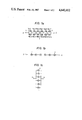
- FIGS. 1a-1c illustrate basic arrangements which may be employed in the practice of this invention.
- FIG. 2 illustrates the embodiment of this invention.
- FIGS. 3a-3b are side views of the apparatus shown in FIG. 2.
- FIG. 1a One of the basic arrangements of this invention is illustrated in FIG. 1a.
- Photovoltaic devices 1 are respectively given numbers from 1 to 12.
- the photovoltaic devices No. 1 and No. 2 are connected together in parallel and in reverse direction. It can be easily understood that with this sort of connection there is no electric output when both the photovoltaic devices No. 1 and No. 2 are irradiated over the whole of their surfaces.
- a pair of photovoltaic devices connected in this way is hereinafter referred to as "a unit”.
- Photovoltaic devices No. 3 and No. 4, No. 5 and No. 6, No. 7 and No. 8, No. 9 and No. 10, and No. 11 and No. 12 also respectively compose units and are connected in series.
- a cash card incorporated with the photoelectric conversion apparatus of this invention has a discriminating faculty that allows users to employ it only in a cash dispenser having a particular irradiating pattern.
- This discriminating faculty does not have the defect of being influenced by a magnetic field as in the case of maintaining records by magnetic recording, nor does it have the disadvantage of disappearing when the power supply is cut off as in the case of a semiconductor memory.
- This faculty is in contrast simple, and has high reliability.
- FIGS. 1b and 1c Other basic arrangements of this invention are respectively illustrated in FIGS. 1b and 1c.
- Each unit may be composed of more than two photovoltaic devices. As a matter of course, there will be no problem even if the characteristics of the devices are different from each other.
- the photo-electric conversion apparatus of this invention can, of course, be incorporated in any kind of electronic system, as well as in ID cards and cash cards provided with electronic devices such as ICs, LSIs, etc.
- the photovoltaic devices employed in this invention are so-called “solar cells” made from Si, GaAs, amorphous Si, etc, it is also possible to dispose a multiplicity of units on a single substrate.
- This photo-electric conversion apparatus can, of course, be used as a power supply for electronic systems, or it can be applied to them merely as an identifying apparatus.
- each unit On connecting the units, resistances, diodes, etc. can also be connected to them, according to need. It is possible for each unit itself to include electronic elements such as resistances, diodes, etc. in addition to the solar cells.
- a photo-electric conversion apparatus e.g., so-called solar cells
- a discriminating faculty for a pattern of irradiated light which will popularize the electronic systems equipped with such a low-cost discriminating faculty, and have a tremendous influence upon the current momentum toward the so-called "information society”.
- FIG. 2 is a plan view of a unit consisting of two photovoltaic devices.
- FIG. 3(a) is a side elevation as viewed in the direction indicated by the arrow I of FIG. 2.
- FIG. 3(b) is a side elevation as viewed in the direction indicated by the arrow II of FIG. 2.
- a transparent electrode 20 is formed using conductive glass.
- amorphous Si layer 3 is formed, consisting of three layers: p-type, intrinsic, and n-type layers; the respective film thickness of these layers are 100 ⁇ , 5000 ⁇ , and 300 ⁇ .
- Electrodes 4 are formed on the layer 3. The points A and B thereon are terminals for connection to other units.
Landscapes
- Photovoltaic Devices (AREA)
Applications Claiming Priority (2)
| Application Number | Priority Date | Filing Date | Title |
|---|---|---|---|
| JP15525684A JPS6135571A (ja) | 1984-07-27 | 1984-07-27 | 光電変換装置 |
| JP59-155256 | 1984-07-27 |
Publications (1)
| Publication Number | Publication Date |
|---|---|
| US4642412A true US4642412A (en) | 1987-02-10 |
Family
ID=15601939
Family Applications (1)
| Application Number | Title | Priority Date | Filing Date |
|---|---|---|---|
| US06/759,961 Expired - Fee Related US4642412A (en) | 1984-07-27 | 1985-07-29 | Photo-electronic conversion apparatus with light pattern discriminator |
Country Status (2)
| Country | Link |
|---|---|
| US (1) | US4642412A (enExample) |
| JP (1) | JPS6135571A (enExample) |
Cited By (2)
| Publication number | Priority date | Publication date | Assignee | Title |
|---|---|---|---|---|
| US6461059B2 (en) * | 2000-03-31 | 2002-10-08 | Hitachi, Ltd. | Photo-electronic device and method of producing the same |
| US20090020306A1 (en) * | 2006-07-29 | 2009-01-22 | Protectconnect, Inc. | Adjustable plaster ring cover |
Citations (3)
| Publication number | Priority date | Publication date | Assignee | Title |
|---|---|---|---|---|
| US3672999A (en) * | 1968-12-19 | 1972-06-27 | Nasa | Use of unilluminated solar cells as shunt diodes for a solar array |
| US3925103A (en) * | 1972-10-27 | 1975-12-09 | Trw Inc | Radiation hard solar cell and array |
| US4456782A (en) * | 1981-03-20 | 1984-06-26 | Fuji Electric Co., Ltd. | Solar cell device |
-
1984
- 1984-07-27 JP JP15525684A patent/JPS6135571A/ja active Granted
-
1985
- 1985-07-29 US US06/759,961 patent/US4642412A/en not_active Expired - Fee Related
Patent Citations (3)
| Publication number | Priority date | Publication date | Assignee | Title |
|---|---|---|---|---|
| US3672999A (en) * | 1968-12-19 | 1972-06-27 | Nasa | Use of unilluminated solar cells as shunt diodes for a solar array |
| US3925103A (en) * | 1972-10-27 | 1975-12-09 | Trw Inc | Radiation hard solar cell and array |
| US4456782A (en) * | 1981-03-20 | 1984-06-26 | Fuji Electric Co., Ltd. | Solar cell device |
Cited By (2)
| Publication number | Priority date | Publication date | Assignee | Title |
|---|---|---|---|---|
| US6461059B2 (en) * | 2000-03-31 | 2002-10-08 | Hitachi, Ltd. | Photo-electronic device and method of producing the same |
| US20090020306A1 (en) * | 2006-07-29 | 2009-01-22 | Protectconnect, Inc. | Adjustable plaster ring cover |
Also Published As
| Publication number | Publication date |
|---|---|
| JPS6135571A (ja) | 1986-02-20 |
| JPH0576790B2 (enExample) | 1993-10-25 |
Similar Documents
| Publication | Publication Date | Title |
|---|---|---|
| EP1218946B1 (en) | Apparatus for localizing production errors in a photovoltaic element | |
| KR0138114B1 (ko) | 집적 회로의 다중 전원 접속부 검사 방법 및 그 장치 | |
| US4826777A (en) | Making a photoresponsive array | |
| US4513167A (en) | Arrays of polarized energy-generating elements | |
| KR100374433B1 (ko) | 배선반에서와이어의결함을탐지하는장치 | |
| US6020555A (en) | System for protecting series connected solar panels against failure due to mechanical damage of individual solar cells while maintaining full output of the remaining cells | |
| DE69232932D1 (de) | Vergrabener kontakt, miteinander verbundene dünnschicht- und grossvolumige photovoltaische zellen | |
| CN109766983A (zh) | 射频芯片、电子标签、检测模块、芯片防转移方法、物件形状及位移检测方法 | |
| US4785191A (en) | Interconnected array of photosensors for simultaneously sensing light intensities at each of a number of locations | |
| US6316955B1 (en) | Photoelectric conversion integrated circuit device | |
| US4642412A (en) | Photo-electronic conversion apparatus with light pattern discriminator | |
| US4348636A (en) | Integrated circuit tester | |
| ATE145286T1 (de) | Diamantdetektor für strahlung | |
| CA1041662A (en) | Apparatus for the storage and reading of data combined from binary numbers | |
| Eisgruber et al. | Extraction of individual‐cell photocurrents and shunt resistances in encapsulated modules using large‐scale laser scanning | |
| JPS58158977A (ja) | 薄膜太陽電池を製造する方法及び装置 | |
| JP2001102604A (ja) | 光電変換装置の製造工程管理方法 | |
| US5404112A (en) | Test method and device for diodes with exposed junction assembled in parallel | |
| US4081820A (en) | Complementary photovoltaic cell | |
| JPH06302851A (ja) | ビーム位置検出器 | |
| GB907119A (en) | Improvements in or relating to bi-stable electric circuit arrangements and apparatusfor intelligence storage embodying such arrangements | |
| Bergner et al. | Obic-Investigations Of Integrated Circuits Using A Laser Scanning Microscope With Different Excitation Wavelengths | |
| Fraas et al. | High efficiency GaAs/GaSb tandem solar cells and tandem circuit cards | |
| US3525981A (en) | Method and system for detection of pattern features | |
| JPS614284A (ja) | 光起電力素子の製造方法 |
Legal Events
| Date | Code | Title | Description |
|---|---|---|---|
| AS | Assignment |
Owner name: HITACHI, LTD., 6, KANDA SURUGADAI 4-CHOME, CHIYODA Free format text: ASSIGNMENT OF ASSIGNORS INTEREST.;ASSIGNORS:MURAMATSU, SHINICHI;SHIMADA, TOSHIKAZU;MATSUBARA, SUNAO;AND OTHERS;REEL/FRAME:004594/0206 Effective date: 19850628 Owner name: HITACHI, LTD., A CORP OF JAPAN,JAPAN Free format text: ASSIGNMENT OF ASSIGNORS INTEREST;ASSIGNORS:MURAMATSU, SHINICHI;SHIMADA, TOSHIKAZU;MATSUBARA, SUNAO;AND OTHERS;REEL/FRAME:004594/0206 Effective date: 19850628 |
|
| FEPP | Fee payment procedure |
Free format text: PAYOR NUMBER ASSIGNED (ORIGINAL EVENT CODE: ASPN); ENTITY STATUS OF PATENT OWNER: LARGE ENTITY |
|
| FPAY | Fee payment |
Year of fee payment: 4 |
|
| FPAY | Fee payment |
Year of fee payment: 8 |
|
| REMI | Maintenance fee reminder mailed | ||
| LAPS | Lapse for failure to pay maintenance fees | ||
| FP | Lapsed due to failure to pay maintenance fee |
Effective date: 19990210 |
|
| STCH | Information on status: patent discontinuation |
Free format text: PATENT EXPIRED DUE TO NONPAYMENT OF MAINTENANCE FEES UNDER 37 CFR 1.362 |