US4620195A - Method of fabricating an ink droplet generator for an ink jet printer and ink droplet generator fabricated thereby - Google Patents
Method of fabricating an ink droplet generator for an ink jet printer and ink droplet generator fabricated thereby Download PDFInfo
- Publication number
- US4620195A US4620195A US06/700,522 US70052285A US4620195A US 4620195 A US4620195 A US 4620195A US 70052285 A US70052285 A US 70052285A US 4620195 A US4620195 A US 4620195A
- Authority
- US
- United States
- Prior art keywords
- panel
- electrode
- electrodes
- charging
- modules
- Prior art date
- Legal status (The legal status is an assumption and is not a legal conclusion. Google has not performed a legal analysis and makes no representation as to the accuracy of the status listed.)
- Expired - Fee Related
Links
Images

Classifications
-
- B—PERFORMING OPERATIONS; TRANSPORTING
- B41—PRINTING; LINING MACHINES; TYPEWRITERS; STAMPS
- B41J—TYPEWRITERS; SELECTIVE PRINTING MECHANISMS, i.e. MECHANISMS PRINTING OTHERWISE THAN FROM A FORME; CORRECTION OF TYPOGRAPHICAL ERRORS
- B41J2/00—Typewriters or selective printing mechanisms characterised by the printing or marking process for which they are designed
- B41J2/005—Typewriters or selective printing mechanisms characterised by the printing or marking process for which they are designed characterised by bringing liquid or particles selectively into contact with a printing material
- B41J2/01—Ink jet
- B41J2/015—Ink jet characterised by the jet generation process
- B41J2/02—Ink jet characterised by the jet generation process generating a continuous ink jet
-
- B—PERFORMING OPERATIONS; TRANSPORTING
- B41—PRINTING; LINING MACHINES; TYPEWRITERS; STAMPS
- B41J—TYPEWRITERS; SELECTIVE PRINTING MECHANISMS, i.e. MECHANISMS PRINTING OTHERWISE THAN FROM A FORME; CORRECTION OF TYPOGRAPHICAL ERRORS
- B41J2/00—Typewriters or selective printing mechanisms characterised by the printing or marking process for which they are designed
- B41J2/005—Typewriters or selective printing mechanisms characterised by the printing or marking process for which they are designed characterised by bringing liquid or particles selectively into contact with a printing material
- B41J2/01—Ink jet
- B41J2/07—Ink jet characterised by jet control
- B41J2/075—Ink jet characterised by jet control for many-valued deflection
- B41J2/08—Ink jet characterised by jet control for many-valued deflection charge-control type
- B41J2/085—Charge means, e.g. electrodes
-
- B—PERFORMING OPERATIONS; TRANSPORTING
- B41—PRINTING; LINING MACHINES; TYPEWRITERS; STAMPS
- B41J—TYPEWRITERS; SELECTIVE PRINTING MECHANISMS, i.e. MECHANISMS PRINTING OTHERWISE THAN FROM A FORME; CORRECTION OF TYPOGRAPHICAL ERRORS
- B41J2/00—Typewriters or selective printing mechanisms characterised by the printing or marking process for which they are designed
- B41J2/005—Typewriters or selective printing mechanisms characterised by the printing or marking process for which they are designed characterised by bringing liquid or particles selectively into contact with a printing material
- B41J2/01—Ink jet
- B41J2/07—Ink jet characterised by jet control
- B41J2/075—Ink jet characterised by jet control for many-valued deflection
- B41J2/08—Ink jet characterised by jet control for many-valued deflection charge-control type
- B41J2/09—Deflection means
-
- B—PERFORMING OPERATIONS; TRANSPORTING
- B41—PRINTING; LINING MACHINES; TYPEWRITERS; STAMPS
- B41J—TYPEWRITERS; SELECTIVE PRINTING MECHANISMS, i.e. MECHANISMS PRINTING OTHERWISE THAN FROM A FORME; CORRECTION OF TYPOGRAPHICAL ERRORS
- B41J2202/00—Embodiments of or processes related to ink-jet or thermal heads
- B41J2202/01—Embodiments of or processes related to ink-jet heads
- B41J2202/22—Manufacturing print heads
Definitions
- the present invention broadly relates to ink jet printers and, more specifically, pertains to a new and improved method of fabricating component parts of an ink droplet generator for generating a sequence of charged, detected and deflected ink droplets for an ink jet printer as well as an arrangement of the components of such ink droplet generator.
- the method of the present invention is for fabricating an ink droplet generator for an ink jet printer wherein a succession of ink droplets is charged, detected or monitored and deflected, while the arrangement of the present invention, namely the ink droplet generator comprises electrode means for the ink droplet generator, of the ink jet printer for generating a succession of charged, detected or monitored and deflected ink droplets.
- an electromagnetic device provided with appropriate means is required. Individual ink droplets are charged, detected or monitored and deflected by a device associated with an ink jet propulsion member or nozzle to create a character image or data pattern at an appropriately designated character position or data field.
- Another and more specific object of the present invention aims at providing a new and improved method of fabricating components of an ink droplet generator of an ink jet printer and an improved ink droplet generator constructed from such fabricated components which permit, on the one hand, the functionally reliable generation of charged, monitored or detected and deflected ink droplets and, on the other hand, the reliable generation of continuous graphic representations in an ink jet printer.
- a further significant object of the present invention aims at providing a new and improved ink droplet generator of the character described which is relatively simple in construction and design, extremely economical to manufacture, highly reliable in operation, not readily subject to breakdown and malfunction and requires a minimum of maintenance and servicing.
- the method of the present invention is manifested by the features that: the means provided for charging, detecting or monitoring and deflecting the ink droplets are formed in a predetermined desired configuration and in mutual electrical isolation by removing unrequired electrically conductive superstrate of metallically coated or plated elements; a first means defining the charging means are formed as charging electrodes, a second means defining the detecting means are formed as detection or monitoring electrodes, and a third means defining the deflection means are formed as deflection electrodes; and a foil or insulating layer resistant to organic or inorganic media, or both, is applied to at least one side of each of the individual first, second and third means and which at least one side is wetted by the ink droplet medium.
- the method of the present invention is manifested by the features that it comprises the steps of: forming and appropriately configuring mutually electrically isolated charging electrode means for imparting an electrostatic charge to the ink droplets by removing undesired portions of a conductive superstrate of at least one circuit board; forming and appropriately configuring mutually electrically isolated detection electrode means for monitoring the ink droplets by removing undesired portions of a conductive superstrate of at least one circuit board; forming and appropriately configuring mutually electrically isolated deflection electrode means for deflecting the ink droplets into a desired trajectory by removing undesired portions of a conductive superstrate of at least one circuit board; each of the charging electrode means, the detection electrode means and the deflection electrode means having a side which is wetted in the ink jet printer by the ink droplets; and applying a protective layer resistant to organic and inorganic agents to the wetted sides.
- the ink droplet generator of the present invention is manifested by the features that it comprises a first module with two first support panels or panel-like support elements arranged in mutually spaced relationship by a spacer component and provided with the charging and detection electrodes and a second module with two support panels or panel-like second support elements arranged in mutually spaced relationship by a spacer component and provided with the deflection electrodes.
- the arrangement of the present invention is manifested by the features that it comprises: a first module comprising a first spacer component and first and second rigid support panels arranged in mutually spaced relationship by the first spacer component; a first charging electrode for imparting an electrostatic charge to the ink droplets and a first detection electrode for detecting the electrostatically charged ink droplets, both formed in mutual electrical isolation upon a first side of the first rigid support panel of the first module; a second charging electrode for imparting an electrostatic charge to the ink droplets and a second detection electrode for detecting the electrostatically charged ink droplets, both formed in mutual electrical isolation upon a first side of the second rigid support panel of the first module; a second module comprising a second spacer component and third and fourth rigid support panels arranged in mutually spaced relationship by the second spacer component; a first deflection electrode for deflecting the electrostatically charged ink droplets into a desired trajectory and formed upon the third rigid support panel of the second module; and a second deflection electrode for de
- a particular advantage which ensues from the method of the present invention is that the means for generating the charged, monitored and deflected ink droplets can be fabricated economically and with optimum electrical properties by employing known circuit board fabrication technology.
- a further advantage consists in that a substantially narrower and smaller structural form is achieved due to the board or panel-like means or components as contrasted to the cumbersome means known heretofore.
- a substantial advantage furthermore consists in that a plurality of ink jet propulsion members or nozzles can be arranged in mutually close spacing when both support elements containing the ink droplet deflection means are fabricated in sandwich construction. Continuous graphic representations are then attainable without further technological expense.
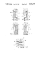
- FIG. 1 schematically shows a perspective representation of an ink droplet generator having means for charging, monitoring and deflecting ink droplets in an ink jet printer;
- FIG. 2 schematically shows a sectional view of one half of the ink droplet generator formed from a first and a second module as depicted in FIG. 1;
- FIG. 3 schematically shows the second module in end view as seen in the direction of the arrow A in FIG. 1;
- FIG. 4 schematically shows one half of the second module viewed in section taking along the line IV--IV in FIG. 2;
- FIGS. 5 through 8 schematically show details of the first module in frontal view
- FIG. 9 schematically shows an arrangment for an ink jet printer formed from a plurality of adjacently arranged modules of adjacently arranged ink droplet generators and ink jet propulsion members or nozzles.
- FIG. 1 of the drawings the apparatus illustrated therein by way of example and not limitation and fabricated by the method as hereinbefore described will be seen to comprise an ink droplet generator or arrangement 50 composed of predetermined component parts or means for charging, detecting or monitoring and deflecting ink droplets in an ink jet printer.
- the ink droplet generator or arrangement 50 comprises a first module 25 with means for charging and detecting or monitoring ink droplets as well as a second module 45 with means for deflecting the ink droplets.
- a schematically represented ink jet propulsion member or nozzle 60 is further visible in FIG. 1.
- the ink droplet generator or arrangement 50 is supplied with a number of ink droplets, simply represented by a line 65 in FIG. 1, by the ink jet propulsion member or nozzle 60.
- the ink droplets follow a trajectory through the first module 25, which is formed substantially from two board or panel-like support elements 5 and 10 arranged in mutually spaced relationship by a spacer component 15, as well as through the second module 45, which is substantially formed from two board or panel-like support elements 30 and 40 arranged in mutually spaced relationship by a spacer component 35.
- FIG. 2 shows a portion of the ink droplet generator or arrangement 50 in sectional view without the two spacer components 15 and 35.
- the support element 5 of the first module 25 as well as the support element 40 of the second module 45 are visible.
- the support element 40 of the second module 45 is represented in FIG. 4 in section taken along the line IV--IV in FIG. 2.
- the second module 45 is represented in FIG. 3 in an end view taken in the direction of the arrow A in FIG. 1. Both support elements 30 and 40 arranged in mutually spaced relationship by the spacer component 35 are visible.
- FIG. 5 shows the first support element 5 in side view.
- This first support element 5 is formed from a polyimide substrate provided with a superstrate of metal coating or plating, such as copper or silver-plated copper.
- the means for charging and detecting or monitoring the ink droplets are formed by removing unrequired superstrate in the desired configuration from one surface or face 5'.
- a charging electrode is designated with the reference numeral 8 and a detection or monitoring electrode is designated with the reference numeral 7 in FIG. 5.
- the detection or monitoring electrode 7 is preferably surrounded by an electromagnetic interference shielding 6 formed from the superstrate and is thereby isolated from the charging electrode 8, on the one hand, and from a deflection electrode 41 (cf. FIG. 2) of the second module 45, on the other hand.
- the elements 6, 7 and 8 are connected with an electrical connection location or terminals 1, 2, 3 and 4 by means of appropriately formed and appropriately mutually arranged conductive traces or current paths 6', 7' and 8'.
- FIG. 7 shows the other surface or face of the first support element 5, which is also provided with a superstrate of metal coating or plating, such as copper or silver-plated copper, not particularly designated.
- An electromagnetic interference shielding 9 is provided on this surface by removing unrequired superstrate.
- the electromagnetic interference shielding 9 corresponds in its external configuration to the electrode means 6 through 8 provided on the other surface or face (cf. FIG. 5).
- the electromagnetic interference shielding 9 is further connected to the electrical connections or terminals 2, 3, and 4 by means of two conductive traces or current paths 9' and 9" formed from the superstrate.
- the second support element 10 is represented in FIGS. 6 and 8.
- This second support element 10 is also formed from a polyimide substrate coated or plated with metal, such as copper or silver-plated copper.
- the electrode means 11, 11'; 12, 12' and 13, 13' are provided on one surface or face 10' by removing unrequired superstrate and an electromagnetic interference shielding 14 configured in correspondence to the electrode means 11, 11'; 12, 12' and 13, 13' is provided on the other not particularly designated surface or face.
- the electromagnetic shielding 14 is connected to electrical connections or terminals 2' and 4' by conductive traces or current paths 14', 14".
- the first charging electrode 8 formed upon the first support element 5 carries a first charging potential and the first detection electrode 7 formed upon the first support element 5 carries a first detecting potential.
- first charging and detecting potentials may be equal in value.
- the second charging electrode 13 formed upon the second support element 10 carries a second charging potential and the second detection electrode 12 formed upon the second support element 10 carries a second detecting potential.
- These second charging and detection potentials while advantageously different from the first charging and detecting potentials, may be equal to one another.
- the electrically conductive and insulative means 6, 6'; 7, 7'; 8, 8'; 9, 9"; 11, 11'; 12, 12'; 13, 13' and 14, 14', 14" formed substantially from the superstrate of metal coating or plating are shown cross-hatched in FIGS. 2 and 5 through 8 for better representational clarity.
- the electrically conductive means provided on each surface of the individual support elements 5 and 10 and having a thickness in the ⁇ -range are insulated from one another by applying a foil resistant to organic and inorganic media, especially by applying a preferably transparent foil 5", 10" resistant to ketone fluid to both support elements 5 and 10 of the first module 25.
- the individual support elements 5, 10 can be formed as hermetically sealed units by applying the foil 5", respectively 10", on both sides.
- the half of the second module 45 seen in section in FIG. 2 shows the support element 40 formed from a substrate 40".
- the support element 40 is provided with a polyimide foil 42 having a superstrate of metallic coating or plating, such as copper or silver-plated copper.
- the deflection electrode 41 formed as a field sector as well as the conductive trace or current path 41' formed as a current lead are formed by removing unrequired superstrate.
- the foil 42 has the external configuration of the support element 40' in its lower region and is formed somewhat wider on both sides than the conductive trace or current path 41' in its upper region.
- a transparent polyimide foil 42' for electrically insulating the deflection electrode 41 as well as the conductive trace or current path 41' is applied to the first foil 42.
- the transparent foil 42' substantially conforms to the external configuration of the first polyimide foil 42.
- the support element 40 fabricated in sandwich construction is schematically shown in FIG. 4 in section taken along the line IV--IV.
- the substrate 40" as well as the polyimide foil 42 applied thereto, the components 41, 41' as well as the second foil 42' are visible.
- the foils 42, 42' are represented in dotted line in FIG. 4 for improved clarity.
- the first support element 30 of the second module 45 is formed analogously to the previously described support element 40.
- the deflection electrode 41 formed on the foil 42 carries a first deflection potential and a corresponding deflection electrode 31 formed on a confronting foil 32 carries a second deflection potential.
- foils 42, 42' are shown partially broken away in FIG. 2 and the foils 5" and 10" are shown partially broken away in FIGS. 5 and 6 for better representational clarity.
- the ink droplet generator or arrangement 50 substantially comprising both modules 25 and 45 forms a unit as represented in FIG. 1 and can be fastened to a not particularly shown conventional support member with relatively simple means.
- both charging electrodes 8, 13 and both detection or monitoring electrodes 7, 12 of the first module 25 as well as the deflection electrodes 41, 31 of the second module 45 are arranged in mirror image relationship to one another as partially indicated in FIG. 1.
- the second module 45 is arranged staggered in height in relation to the first module 25 such that the ink droplet stream or jet 65 emitted by the ink jet propulsion member or nozzle 60 has a trajectory passing approximately through the middle region of both deflection electrodes 31, 41 arranged in mirror image relationship to one another and is deflected at that region into a desired trajectory.
- both support elements 5, 10 as well as the spacer component 15 are operatively or electrically interconnected with one another by means of plated-through electrical connection locations or terminals 1, 1'; 2, 2'; 3, 3' and 4, 4':Corresponding electrical leads or conductors 16, 17, 17' and 18 are conducted to the individual connection locations or terminals, as schematically shown in FIG. 2.
- FIG. 9 An arrangement 100 is schematically shown in FIG. 9 which is formed from a plurality of individual ink droplet generators 50 as hereinbefore described.
- This arrangement 100 also comprises a plurality of ink jet propulsion members or nozzles 60 through 60n, a plurality of first modules 25 through 25n as well as a plurality of second modules 46 through 46n.
- the ink droplets from the ink jet propulsion members or nozzles 60 through 60n represented by the lines 65 through 65n are charged and monitored or detected in each respective first module 25 through 25n and deflected in each respective second module 45 through 45n to an associated recording medium 90.
- the not particularly designated support elements 30 through 30n and 40 through 40n of the second modules 46 through 46n be provided with metal coating or plating on both sides and that each side oriented parallel to the trajectory of the ink droplets be provided with not particularly shown and not particularly designated conductive traces or current paths.
- These conductive traces or current paths are formed analogously to the conductive traces or current paths 31', 41' of the second module 45.
Applications Claiming Priority (2)
| Application Number | Priority Date | Filing Date | Title |
|---|---|---|---|
| CH93984 | 1984-02-27 | ||
| CH939/84 | 1984-02-27 |
Publications (1)
| Publication Number | Publication Date |
|---|---|
| US4620195A true US4620195A (en) | 1986-10-28 |
Family
ID=4198693
Family Applications (1)
| Application Number | Title | Priority Date | Filing Date |
|---|---|---|---|
| US06/700,522 Expired - Fee Related US4620195A (en) | 1984-02-27 | 1985-02-11 | Method of fabricating an ink droplet generator for an ink jet printer and ink droplet generator fabricated thereby |
Country Status (5)
| Country | Link |
|---|---|
| US (1) | US4620195A (de) |
| EP (1) | EP0153436B1 (de) |
| AT (1) | ATE51583T1 (de) |
| BE (1) | BE901198A (de) |
| DE (1) | DE3481833D1 (de) |
Cited By (8)
| Publication number | Priority date | Publication date | Assignee | Title |
|---|---|---|---|---|
| FR2676023A1 (fr) * | 1991-05-03 | 1992-11-06 | Imaje | Tete de deflexion multijet modulaire et procede de fabrication. |
| US5475411A (en) * | 1992-05-29 | 1995-12-12 | Scitex Digital Printing, Inc. | Method of fabricating a catcher/charge plate assembly |
| US5754206A (en) * | 1996-02-23 | 1998-05-19 | Scitex Digital Printing, Inc. | Low stress droplet generator mount assembly |
| WO1999059822A1 (en) * | 1998-05-20 | 1999-11-25 | Linx Printing Technologies Plc | Ink jet printer and deflector plate therefor |
| US6120133A (en) * | 1997-02-05 | 2000-09-19 | Samsung Electronics Co., Ltd. | Magnetic ink jetting apparatus |
| EP1013458A3 (de) * | 1998-12-14 | 2000-11-08 | SCITEX DIGITAL PRINTING, Inc. | Monolithisches Tintenstrahldruckchassis |
| US6402299B1 (en) | 1999-10-22 | 2002-06-11 | Lexmark International, Inc. | Tape automated bonding circuit for use with an ink jet cartridge assembly in an ink jet printer |
| US20040017443A1 (en) * | 2002-07-08 | 2004-01-29 | Canon Kabushiki Kaisha | Liquid detection method, liquid detection apparatus and printing apparatus using the liquid detection |
Families Citing this family (3)
| Publication number | Priority date | Publication date | Assignee | Title |
|---|---|---|---|---|
| EP0613778B1 (de) * | 1993-03-01 | 1998-06-10 | SCITEX DIGITAL PRINTING, Inc. | Passivierungsschicht für Ladungselektroden auf Basis von Keramik |
| GB9626686D0 (en) * | 1996-12-23 | 1997-02-12 | Domino Printing Sciences Plc | Continuous inkjet printer |
| FR2763870B1 (fr) * | 1997-06-03 | 1999-08-20 | Imaje Sa | Systeme de commande de projection de liquide electriquement conducteur |
Citations (4)
| Publication number | Priority date | Publication date | Assignee | Title |
|---|---|---|---|---|
| US4121223A (en) * | 1975-09-19 | 1978-10-17 | Hitachi, Ltd. | Ink jet recording apparatus with an improved ink sensor |
| US4338612A (en) * | 1979-10-11 | 1982-07-06 | Ricoh Co., Ltd. | Multiple deflection plate device for liquid jet printer or the like |
| US4368476A (en) * | 1979-12-19 | 1983-01-11 | Canon Kabushiki Kaisha | Ink jet recording head |
| US4568946A (en) * | 1982-11-05 | 1986-02-04 | Willett International Limited | Charge electrode means for ink jet printer |
Family Cites Families (2)
| Publication number | Priority date | Publication date | Assignee | Title |
|---|---|---|---|---|
| US4194211A (en) * | 1978-06-19 | 1980-03-18 | International Business Machines Corporation | Charge electrode array for multi-nozzle ink jet array |
| US4346389A (en) * | 1979-10-11 | 1982-08-24 | Ricoh Co., Ltd. | Multiple charge electrode device for liquid jet printer |
-
1984
- 1984-03-19 AT AT84102986T patent/ATE51583T1/de not_active IP Right Cessation
- 1984-03-19 EP EP84102986A patent/EP0153436B1/de not_active Expired - Lifetime
- 1984-03-19 DE DE8484102986T patent/DE3481833D1/de not_active Expired - Fee Related
- 1984-12-04 BE BE0/214102A patent/BE901198A/fr not_active IP Right Cessation
-
1985
- 1985-02-11 US US06/700,522 patent/US4620195A/en not_active Expired - Fee Related
Patent Citations (4)
| Publication number | Priority date | Publication date | Assignee | Title |
|---|---|---|---|---|
| US4121223A (en) * | 1975-09-19 | 1978-10-17 | Hitachi, Ltd. | Ink jet recording apparatus with an improved ink sensor |
| US4338612A (en) * | 1979-10-11 | 1982-07-06 | Ricoh Co., Ltd. | Multiple deflection plate device for liquid jet printer or the like |
| US4368476A (en) * | 1979-12-19 | 1983-01-11 | Canon Kabushiki Kaisha | Ink jet recording head |
| US4568946A (en) * | 1982-11-05 | 1986-02-04 | Willett International Limited | Charge electrode means for ink jet printer |
Cited By (13)
| Publication number | Priority date | Publication date | Assignee | Title |
|---|---|---|---|---|
| FR2676023A1 (fr) * | 1991-05-03 | 1992-11-06 | Imaje | Tete de deflexion multijet modulaire et procede de fabrication. |
| EP0512907A1 (de) * | 1991-05-03 | 1992-11-11 | Imaje S.A. | Modular aufgebauter Mehrfachdüsenkopf mit Ablenksteuerung und Verfahren zu seiner Herstellung |
| US5394180A (en) * | 1991-05-03 | 1995-02-28 | Imaje S.A. | Modular multijet deflection head and manufacturing method |
| US5475411A (en) * | 1992-05-29 | 1995-12-12 | Scitex Digital Printing, Inc. | Method of fabricating a catcher/charge plate assembly |
| US5754206A (en) * | 1996-02-23 | 1998-05-19 | Scitex Digital Printing, Inc. | Low stress droplet generator mount assembly |
| US6120133A (en) * | 1997-02-05 | 2000-09-19 | Samsung Electronics Co., Ltd. | Magnetic ink jetting apparatus |
| WO1999059822A1 (en) * | 1998-05-20 | 1999-11-25 | Linx Printing Technologies Plc | Ink jet printer and deflector plate therefor |
| US6357860B1 (en) | 1998-05-20 | 2002-03-19 | Linx Printing Technologies Plc | Ink jet printer and deflector plate therefor |
| US6467880B2 (en) | 1998-05-20 | 2002-10-22 | Linx Printing Technologies Plc | Ink jet printer and deflector plate therefor |
| EP1013458A3 (de) * | 1998-12-14 | 2000-11-08 | SCITEX DIGITAL PRINTING, Inc. | Monolithisches Tintenstrahldruckchassis |
| US6402299B1 (en) | 1999-10-22 | 2002-06-11 | Lexmark International, Inc. | Tape automated bonding circuit for use with an ink jet cartridge assembly in an ink jet printer |
| US20040017443A1 (en) * | 2002-07-08 | 2004-01-29 | Canon Kabushiki Kaisha | Liquid detection method, liquid detection apparatus and printing apparatus using the liquid detection |
| US6988783B2 (en) * | 2002-07-08 | 2006-01-24 | Canon Kabushiki Kaisha | Liquid detection method, liquid detection apparatus and printing apparatus using the liquid detection |
Also Published As
| Publication number | Publication date |
|---|---|
| ATE51583T1 (de) | 1990-04-15 |
| DE3481833D1 (de) | 1990-05-10 |
| BE901198A (fr) | 1985-03-29 |
| EP0153436B1 (de) | 1990-04-04 |
| EP0153436A3 (en) | 1986-03-26 |
| EP0153436A2 (de) | 1985-09-04 |
Similar Documents
| Publication | Publication Date | Title |
|---|---|---|
| US4620195A (en) | Method of fabricating an ink droplet generator for an ink jet printer and ink droplet generator fabricated thereby | |
| US4194083A (en) | Capacitively coupled tablet | |
| US4054939A (en) | Multi-layer backpanel including metal plate ground and voltage planes | |
| CN101600293B (zh) | 印刷电路板 | |
| US6467880B2 (en) | Ink jet printer and deflector plate therefor | |
| US2907925A (en) | Printed circuit techniques | |
| GB2161988A (en) | Double layer wiring panel | |
| GB1587739A (en) | Charge plate for ink jet printers | |
| US3975741A (en) | Charge electrode for ink jet | |
| JPS6325947B2 (de) | ||
| US4385306A (en) | Dot writing head for high definition printers, and a method of manufacturing the same | |
| US5956060A (en) | Electrode assembly on a flexible non-conductive film for a continuous ink jet printer | |
| CN1150087C (zh) | 连续式喷墨打印头用的偏转电极及制造方法和喷墨打印机 | |
| US4568946A (en) | Charge electrode means for ink jet printer | |
| US4035812A (en) | Ink jet recorder and charge ring plate therefor with reduced deplating current | |
| US20110292127A1 (en) | Liquid discharge head | |
| EP0380366B1 (de) | Trägerschicht für Aufzeichnungskopf und Aufzeichnungskopf | |
| EP0744291B1 (de) | Verfahren zur Herstellung von Ladungselektroden | |
| US6302526B1 (en) | Electrode type print head for printing apparatus and method of manufacturing the same | |
| US5019675A (en) | Thick film substrate with highly thermally conductive metal base | |
| US20160212859A1 (en) | Printing electronic circuitry | |
| JP2729858B2 (ja) | ジェット・プリント・ヘッド | |
| JP3030823B2 (ja) | 画像形成装置 | |
| JPS6122958A (ja) | マルチインクジエツト記録装置における荷電電極構造 | |
| JP2000272133A (ja) | インクジェット記録装置のヘッド及びヘッド駆動信号供給路 |
Legal Events
| Date | Code | Title | Description |
|---|---|---|---|
| AS | Assignment |
Owner name: CONTRAVES GMBH, HANS-STIESSBERGER-STRASSE 2A, 8013 Free format text: ASSIGNMENT OF ASSIGNORS INTEREST.;ASSIGNORS:EBELEN, OTTO;GLOCKLER, GERHARD;KOHLER, FRANZ;AND OTHERS;REEL/FRAME:004419/0856 Effective date: 19850201 Owner name: CONTRAVES GMBH, A CORP OF WEST GERMANY, GERMANY Free format text: ASSIGNMENT OF ASSIGNORS INTEREST;ASSIGNORS:EBELEN, OTTO;GLOCKLER, GERHARD;KOHLER, FRANZ;AND OTHERS;REEL/FRAME:004419/0856 Effective date: 19850201 |
|
| FEPP | Fee payment procedure |
Free format text: PAYOR NUMBER ASSIGNED (ORIGINAL EVENT CODE: ASPN); ENTITY STATUS OF PATENT OWNER: SMALL ENTITY |
|
| AS | Assignment |
Owner name: CODI-JET MARKIERUNGS SYSTEME GMBH, HEINRICH-FAHR-S Free format text: ASSIGNMENT OF ASSIGNORS INTEREST.;ASSIGNOR:CONTRAVES GMBH;REEL/FRAME:004857/0117 Effective date: 19880322 Owner name: CODI-JET MARKIERUNGS SYSTEME GMBH, A CORP. OF WEST Free format text: ASSIGNMENT OF ASSIGNORS INTEREST;ASSIGNOR:CONTRAVES GMBH;REEL/FRAME:004857/0117 Effective date: 19880322 |
|
| FEPP | Fee payment procedure |
Free format text: PAT HOLDER CLAIMS SMALL ENTITY STATUS - SMALL BUSINESS (ORIGINAL EVENT CODE: SM02); ENTITY STATUS OF PATENT OWNER: SMALL ENTITY |
|
| FEPP | Fee payment procedure |
Free format text: PAYOR NUMBER ASSIGNED (ORIGINAL EVENT CODE: ASPN); ENTITY STATUS OF PATENT OWNER: SMALL ENTITY Free format text: PAYER NUMBER DE-ASSIGNED (ORIGINAL EVENT CODE: RMPN); ENTITY STATUS OF PATENT OWNER: SMALL ENTITY |
|
| FPAY | Fee payment |
Year of fee payment: 4 |
|
| REMI | Maintenance fee reminder mailed | ||
| LAPS | Lapse for failure to pay maintenance fees | ||
| FP | Lapsed due to failure to pay maintenance fee |
Effective date: 19941102 |
|
| STCH | Information on status: patent discontinuation |
Free format text: PATENT EXPIRED DUE TO NONPAYMENT OF MAINTENANCE FEES UNDER 37 CFR 1.362 |