US4527278A - Method for correcting the frequency of a local carrier in a receiver of a data transmission system and receiver using this method - Google Patents
Method for correcting the frequency of a local carrier in a receiver of a data transmission system and receiver using this method Download PDFInfo
- Publication number
- US4527278A US4527278A US06/483,085 US48308583A US4527278A US 4527278 A US4527278 A US 4527278A US 48308583 A US48308583 A US 48308583A US 4527278 A US4527278 A US 4527278A
- Authority
- US
- United States
- Prior art keywords
- phase
- frequency
- partial correlations
- samples
- sub
- Prior art date
- Legal status (The legal status is an assumption and is not a legal conclusion. Google has not performed a legal analysis and makes no representation as to the accuracy of the status listed.)
- Expired - Lifetime
Links
Images
Classifications
-
- H—ELECTRICITY
- H04—ELECTRIC COMMUNICATION TECHNIQUE
- H04L—TRANSMISSION OF DIGITAL INFORMATION, e.g. TELEGRAPHIC COMMUNICATION
- H04L27/00—Modulated-carrier systems
- H04L27/18—Phase-modulated carrier systems, i.e. using phase-shift keying
- H04L27/22—Demodulator circuits; Receiver circuits
- H04L27/227—Demodulator circuits; Receiver circuits using coherent demodulation
- H04L27/2271—Demodulator circuits; Receiver circuits using coherent demodulation wherein the carrier recovery circuit uses only the demodulated signals
- H04L27/2273—Demodulator circuits; Receiver circuits using coherent demodulation wherein the carrier recovery circuit uses only the demodulated signals associated with quadrature demodulation, e.g. Costas loop
-
- H—ELECTRICITY
- H04—ELECTRIC COMMUNICATION TECHNIQUE
- H04L—TRANSMISSION OF DIGITAL INFORMATION, e.g. TELEGRAPHIC COMMUNICATION
- H04L27/00—Modulated-carrier systems
- H04L27/18—Phase-modulated carrier systems, i.e. using phase-shift keying
- H04L27/22—Demodulator circuits; Receiver circuits
- H04L27/233—Demodulator circuits; Receiver circuits using non-coherent demodulation
- H04L27/2332—Demodulator circuits; Receiver circuits using non-coherent demodulation using a non-coherent carrier
-
- H—ELECTRICITY
- H04—ELECTRIC COMMUNICATION TECHNIQUE
- H04L—TRANSMISSION OF DIGITAL INFORMATION, e.g. TELEGRAPHIC COMMUNICATION
- H04L27/00—Modulated-carrier systems
- H04L27/0014—Carrier regulation
- H04L2027/0024—Carrier regulation at the receiver end
- H04L2027/0026—Correction of carrier offset
- H04L2027/003—Correction of carrier offset at baseband only
-
- H—ELECTRICITY
- H04—ELECTRIC COMMUNICATION TECHNIQUE
- H04L—TRANSMISSION OF DIGITAL INFORMATION, e.g. TELEGRAPHIC COMMUNICATION
- H04L27/00—Modulated-carrier systems
- H04L27/0014—Carrier regulation
- H04L2027/0044—Control loops for carrier regulation
- H04L2027/0053—Closed loops
- H04L2027/0057—Closed loops quadrature phase
-
- H—ELECTRICITY
- H04—ELECTRIC COMMUNICATION TECHNIQUE
- H04L—TRANSMISSION OF DIGITAL INFORMATION, e.g. TELEGRAPHIC COMMUNICATION
- H04L27/00—Modulated-carrier systems
- H04L27/0014—Carrier regulation
- H04L2027/0044—Control loops for carrier regulation
- H04L2027/0063—Elements of loops
- H04L2027/0067—Phase error detectors
-
- H—ELECTRICITY
- H04—ELECTRIC COMMUNICATION TECHNIQUE
- H04L—TRANSMISSION OF DIGITAL INFORMATION, e.g. TELEGRAPHIC COMMUNICATION
- H04L7/00—Arrangements for synchronising receiver with transmitter
- H04L7/04—Speed or phase control by synchronisation signals
- H04L7/041—Speed or phase control by synchronisation signals using special codes as synchronising signal
- H04L7/042—Detectors therefor, e.g. correlators, state machines
Definitions
- the invention relates to a frequency correction method intended to correct the frequency of a local carrier in a receiver of a data transmission system in which the data are transmitted by carrier modulation and a receiver synchronizing word is transmitted before the data, this receiver comprising means for demodulating a received signal with the aid of signals in phase and in quadrature with a local carrier, means for sampling the inphase and quadrature demodulated signals with a sampling frequency equal to the modulation rate, each new pair of in-phase and quadrature samples thus formed being written into a received-signal memory, the receiver further comprising a synchronizing-word memory containing the in-phase and quadrature samples of a local synchronizing word which is identical to the transmitted synchronizing word.
- the invention also relates to a receiver used in a data transmission system, this receiver utilizing this method.
- each communication be preceded by a preamble which comprises, for example, a pure carrier for the synchronization of the local carrier, an alternating sequence of "1" and "0" bits for the synchronization of the local clock and finally a known word for word synchronization.
- a preamble which comprises, for example, a pure carrier for the synchronization of the local carrier, an alternating sequence of "1" and "0" bits for the synchronization of the local clock and finally a known word for word synchronization.
- This acquisition system which comprises phase or frequency control loops for carrier synchronization and clock synchronization, is very slow and is not so suitable for contemporary digital communication systems for data packets in which the duration of the communications can be very short, for example of the order of one second.
- the initial synchronization of the receiver is preferably effected without the use of control loops, by only using a synchronizing word which is transmitted and is known in the receiver.
- a method of this type is described which is based on the calculation of the correlation function between a local synchronizing word, which is identical to the transmitted synchronizing word.
- the received demodulated signal is observed during a time window which is equal to the duration of the synchronizing word.
- local carrier synchronization and local clock synchronization are obtained simultaneously by calculating the phase values of the local carrier and the local clock which maximize the said correlation function. These optimum phase values are obtained by extrapolation on the basis of estimated values which are reasonably close to the optimum values.
- the determination of the local carrier phase is closely connected to the determination of the local clock phase so that it would be rather difficult to employ this method.
- the present invention also permits rapid acquisition of the synchronization of the receiver by using only one synchronizing word transmitted as a preamble before a communication, but by using a totally different method as regards the synchronization of the local carrier.
- the invention provides a method for correcting the frequency of the local carrier, based on measuring the frequency deviations between the local carrier and the received carrier and making it possible to acquire the carrier, clock and frame synchronizations in one sampling period.
- the method is characterized in that, during each sampling period, synchronized reading of n pairs of samples contained in the synchronizing-word memory and n pairs of samples written last into the received-signal memory is effected at least once, in order to determine in P steps (P ⁇ 1) the magnitude of the frequency correction to be effected on the local carrier:
- each step p ⁇ 1 there is calculated from at least one corrected quantity E*, which is formed during the step and which is of the same length as the portions of the synchronizing word used during the step, the frequency deviation ⁇ f p , and thereafter the sum ##EQU2## is formed.
- This sum constitutes an estimate of the magnitude of the frequency correction, this estimate at the end of the step P being the final value to be retained for the magnitude of the frequency correction to be effected on the local carrier.
- the means provided in the receiver to form the partial correlation until the last step P are inter alia controlled, taking account of the final frequency correction calculated at the end of the step P, in order to form the complete in-phase and quadrature correlations relating to the total length of the synchronizing word, additional means being provided to form the sum of the squares of the said complete in-phase and quadrature correlations and to compare this sum with a threshold, exceeding of this threshold indicating at the same time the acquisition of the frame synchronization and the frequency correction to be effected on the local carrier for the transmission of data following this acquisition of frame synchronization.
- a receiver of this type in which the received demodulated signal is sampled with a sampling frequency j/T which is a multiple of the modulation rate 1/T, so as to form j sampled signals having the period T and being interleaved, it is advantageous to effect at the same time the search for frame synchronization and the search for the optimum position of the sampling instants (that is to say the search for local clock synchronization), after the last frequency correction calculating step.
- the means provided in the receiver for forming the magnitude of the frequency corrections and thereafter the sum of the squares of the complete in-phase and quadrature correlations are used in time sharing for each one of the said j interleaved signals, the j sums of the squares of the correlations thus formed during one modulation period being compared with a threshold, exceeding of this threshold indicating at the same time the acquisition of the frame synchronization, the frequency correction to be effected on the local carrier and the optimum position of the sampling instants to be used for the transmission of data following the acquisition of the frame synchronization.
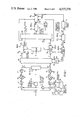
- FIG. 1 is a schematic diagram which shows how the method according to the invention can be employed in the receiver of a data transmission system.
- FIG. 2 illustrates the different steps of the method according to the invention
- the waveforms in 2a show the portions of the synchronizing word used
- the waveforms in 2b represent the corrected quantity E* as a function of the frequency deviation ⁇ f.
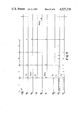
- FIG. 3 shows time diagrams for different signals and different magnitudes calculated during the steps of the method according to the invention.
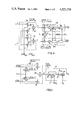
- FIG. 4 is a schematic diagram which shows an embodiment of a phase shifting circuit and a correlation calculation circuit used in a receiver employing the method according to the invention.
- FIG. 5 shows a schematic diagram of the circuits for calculating the quantities E and their mean value.
- FIG. 6 shows a schematic diagram of the circuits for calculating the corrected quantity E* and a term of the frequency deviation ⁇ f.
- FIG. 7 shows a schematic diagram of the circuits for calculating the magnitude of the frequency correction f VCO and the phase correction ⁇ VCO .
- FIG. 8 is a schematic diagram which shows, in accordance with a variant differing from FIG. 1, how the method according to the invention can be employed in the receiver of a data transmission system.
- FIG. 9 shows time diagrams which represent the complete correlation between the local synchronizing word and the received demodulated signal, these diagrams illustrating how it is possible to obtain frame and clock synchronization in a receiver after the last step of the method according to the invention.
- FIG. 10 shows the configuration of a receiver after synchronization has been acquired by means of the method according to the invention.
- FIG. 11 shows time diagrams which complete the diagrams of FIG. 3 and shows control signals used to employ the method according to the invention as shown in the schematic diagrams of FIGS. 1 and 8.
- FIG. 1 shows the schematic diagram of a receiver of a data transmission system in which the frequency correction method according to the invention is employed.
- the remote transmitter (not shown) a carrier in phase-modulated and/or amplitude-modulated or frequency-modulated by the data signal to be transmitted, to form the modulated carrier signal which is transmitted to the receiver via a transmission path of limited bandwidth.
- the transmission is, for example, effected via a radio channel.
- the modulated signal received at an input 1 of the receiver shown in FIG. 1 is applied to two mixers 2 and 3 for demodulation by two local carrier signals whose phases are shifted 90° relative to each other.
- the in-phase local carrier signal supplied directly by a local carrier generator 4 is applied to mixer 2 and the quadrature local carrier signal derived from generator 4 via a 90° phase shifting circuit 5 is applied to mixer 3.
- Two low-pass filters 6 and 7 connected to the output of mixers 2 and 3 remove the frequency components located above the band used for the transmission and supply the in-phase and quadrature demodulated signals s r and s i , respectively.
- signals s r and s i are the real and the imaginary components, respectively, of a base-band signal which is representative of the data signal used to modulate the carrier in the remote transmitter. Thereafter the signals s r and s i are sampled in circuits 8 and 9 at a sampling frequency H which is here assumed to be equal to the modulation rate 1/T in the transmitter, T being the modulation interval.
- the sampling frequency H is supplied by a generator 10 producing a low-frequency local clock derived from a time base generator 11, which has a much higher frequency. If the subsequent processing operations in the receiver are effected in a digital manner, which in practice is the case in a receiver using the method according to the invention, the samples produced in circuits 8 and 9 are there furthermore converted into the digital form.
- the in-phase samples S r and the quadrature samples S i may be applied directly (or via an equalizer) to the decision circuit of the receiver, this decision circuit (not shown) having for its object to recover the data.
- a correct recovery of the data implies in the first place a rigorous frequency and phase synchronization of the local carrier, used for the demodulation in the receiver, with the carrier of the received signal.
- a typical value of the highest permissible difference between the frequencies of these two carriers is 1 Hz, which, related for example to a RF carrier frequency of 30 MHz, corresponds to a precision of 3 10 -8 .
- the frequency of the received carrier may deviate much more than 1 Hz, it is necessary to correct the frequency of the local demodulating carrier before each communication so as to ensure that the difference between the frequencies of this local carrier and the received carrier does not exceed the permissible limit.
- This frame synchronization is obtained in a conventional way by recognizing in the receiver a frame synchronizing word transmitted before each data message. This recognition may be effected by calculating the correlation function between a frame synchronizing word generated locally in the receiver and the samples of the received demodulated signal which are formed with the aid of the in-phase and quadrature Samples S r and S i .
- the above-mentioned article by Meyers and Franks proposes to act simultaneously on the phases of the demodulating carrier and the sampling clock so as to maximize the correlation function calculated for acquiring frame synchronization.
- the present invention while using the frame synchronization sequence, operates in a different manner and provides a frequency corection method for the local carrier which is performed completely during one sampling period and, at the end of this period, permits acquiring the carrier synchronization, the frame synchronization and the sampling clock synchronization.
- the modulated signal, transmitted by the remote transmitter may be written:
- A is the amplitude of the carrier
- ⁇ is the angular frequency of the carrier
- the coherent demodulation of the received signal may be effected in the receiver by beating the received signal with a local carrier of the same frequency and the same phase as the carrier of the received signal.
- This beating operation is effected in mixer 2 and, assuming the received signal to have exactly the shape of the transmitted signal a(t), it corresponds to the expression:
- the demodulated signal is written:
- the demodulated signal is effected by an amplitude modulation at the rate of the frequency deviation ⁇ f.
- This amplitude modulation may seriously disturb the correct recovery of the data in the decision circuit of the receiver.
- the detection of the frame synchronizing word transmitted before each data message is also effected by a frequency difference between the local carrier and the carrier of the received signal. If the synchronizing word comprises n bits, this detection is effected in a customary manner by calculating the correlation function G between a local copy of the synchronizing word and the demodulated signal.
- ⁇ l an integer which varies from 0 to n-1
- ⁇ K a sequence of n data bits contained in the received signal
- the duration of a bit being the modulation period T the correlation function G is written, using formula (1): ##EQU3##
- G m may be written as: ##EQU5##
- the method according to the invention has for its object to correct this frequency deviation ⁇ f to enable first the correct detection of the frame synchronizing word, and then the correct demodulation of the transmitted data after frame synchronization has been acquired.
- This method is based on an evaluation of the average phase deviation due to this frequency deviation and existing between two equal and consecutive portions of the synchronizing word. First the case will be considered in which these two portions are two halves of the synchronizing word. For the case of a synchronizing word having n bits, the phase deviation between the two blocks forming the two halves of this word is:
- N n/2 being the number of bits of each block.
- the in-phase and quadrature samples of the demodulated received signal and the in-phase and quadrature samples of the local synchronizing word are used and 4 correlation functions are calculated which will be denoted partial correlations hereinafter as they each relate to a portion of the synchronizing word.
- the partial correlation C i 1 which is similar to the partial correlation C r 1 , but uses quadrature samples;
- the partial correlation C i 2 which is similar to the partial correlation C r 2 , but uses quadrature samples.
- the error E thus calculated also depends on the level of the received signal.
- the error E may be corrected by dividing it by a correction term equal to the sum of the squares of the in-phase and quadrature samples of the demodulated received signal. In this way a corrected error E* is obtained which only depends on the phase deviation ⁇ and is such that: ##EQU8##
- a frequency correction method based on the correlations on two halves of the synchronizing word offers a certain limitation as regards the domain of the measurable frequency deviation ⁇ f.
- the corrected error E* which may now be assumed to be equal to sin ⁇ , it is necessary that
- the considered arrangement can only measure and consequently correct frequency deviations which are less than a maximum value ⁇ f max such that:
- the maximum measurable frequency deviation ⁇ f max may be insufficient to correct the actual frequency deviation.
- the frequency correction method effecting the partial correlations on the portions of the length N' is capable of measuring a frequency deviation up to ⁇ f' max such that:
- the invention proposes to operate in several steps during each of which a frequency deviation is measured by using portions of the synchronizing word of a predetermined length and at the end of which a frequency correction corresponding to the measured deviation is effected.
- the measurements are effected with portions of increasing lengths so that the range of measurable frequency deviations decreases.
- the frequency corrections are effected at the end of each step before the following measurement is performed, the frequency deviations to be measured in the sequence of steps also decrease, while the measuring precision increases.
- the error E corrected as regards its dependence on the level of the received signal that is the corrected error E*, has the value: ##EQU11## where ⁇ is the phase deviation between the two portions of the synchronizing word and b is the number of bits of each of these portions.
- the corrected error E* has substantially the value:
- phase deviation ⁇ f can be obtained.
- the frequency deviation ⁇ f which gave rise to this phase deviation ⁇ for two b-bit portions can be obtained with the aid of the relation:
- a frequency deviation ⁇ f p is determined at the end of each step p and therefore the sum ##EQU12## which for this step constitutes a certain estimate of the magnitude of the frequency correction to be effected on the local carrier.
- This sum formed at the end of the last step P is the value to be retained for this frequency correction during the data transmission after frame synchronization has been acquired.
- the maximum frequency deviation determines the maximum length of the smallest portions of the synchronizing word used in the first step where the frequency deviation measurement is the least precise.
- the final precision required determines the minimum length of the two portions used in the last step.
- a method utilizing P steps may be implemented by dividing the n bit synchronizing word into elementary portions having the following respective number of bits: n/2 P , n/2 P-1 , . . . n/2 2 , n/2.
- the two constrains mentioned above will be respected when the smallest portions of n/2 P bits allow an effective measurement of the initial frequency deviation imposed and when the two largest portions of n/2 bits provide the measurement with the required precision.
- the phase deviation ⁇ 1 can be derived therefrom and thereafter the frequency deviation ⁇ f 1 using the relation
- the frequency of the local carrier is corrected for the measured frequency deviation ⁇ f 1 , which works out in a correction of the phase of the demodulated signal to be correlated with the portions of the synchronizing word used in the subsequent step 2.
- Estimating the frequency deviation ⁇ f 3 may be done by calculating 3 errors E of which the average value is taken.
- the measured frequency deviation ⁇ f 3 is taken into account for the correction of the phase of the demodulated signal to be correlated with the portions of the synchronizing word in the subsequent step 4.
- the frequency deviation ⁇ f 4 is measured by calculating the error E from the two halves of the synchronizing word.
- the frequency deviation measured may be taken account of for the correction of the phase of the demodulated signal which, in a following step not being part of the frequency correction procedure proper, may be correlated with the total synchronizing word with the object of acquiring frame synchronization and, possibly, sampling clock synchronization, as will be explained hereinafter.
- the frequency correction of the local carrier to be retained is the sum of the 4 frequency deviations measured, namely ⁇ f 1 + ⁇ f 2 + ⁇ f 3 +f 4 .
- This frequency correction is effectively used for the demodulation of the received signal, when frame synchronization is obtained.
- the frequency correction arrangement comprises a memory 12 which can be connected to the output of circuits 8 and 9 via gate circuits 13 and 14, which are shown in the form of contacts. These gate circuits are controlled by a signal H' produced by a sequencing circuit 29 for storing in memory 12 each pair of samples S r and S i produced by circuits 8 and 9. Sequencing circuit 29 receives pulses from time base 11 and supplies all the other control signals necessary for the operation of the arrangement.
- Memory 12 is dimensioned for storing pairs of samples S r and S i of which there are as many as the number n of bits of the synchronizing word. These stored samples S r , S i , may be in the analog or the digital form, depending on the technique employed in the arrangement, Diagram 3a in FIG. 3 shows two consecutive pulses of the signal H' which are separated by the period T of the sampling operation effected in circuits 8 and 9. Let it be assumed for the moment that this period is the same as the modulation period T.
- memory 12 receives a fast read clock signal h having a frequency which is sufficient to ensure that during the period T there appear at two outputs of the memory as many sequences of n samples S r and n samples S i as is necessary for a complete cycle of the procedure.
- the signals x and y appearing at the two outputs of memory 12 are the real and imaginary components of a complex signal z. They are applied to a phase shifter 15, whose object is to have the phase of each sample of each sequence of n samples of the complex signal z shift through a phase angle ⁇ VCO corresponding to the frequency correction f VCO produced by the frequency correction circuit at the end of each step.
- Phase shifter 15 supplies the real and imaginary components X and Y of a complex signal Z, by effecting the calculation: ##EQU13##
- phase shifter 15 The quantities sin ⁇ VCO and cos ⁇ VCO used in phase shifter 15 are provided by a read-only memory (ROM) 16 which is addressed by the phase ⁇ VCO produced by a phase generator 17 at the rate of the fast clock h.
- ROM read-only memory
- Generator 17 produces the phase ⁇ VCO on the basis of the frequency correction f VCO supplied by a frequency correction generator 18.
- the samples of the signals X and Y are applied to the correlation calculation circuits 19 and 20 to which also the samples of the real and imaginary components X' and Y' of the local synchronizing word are applied.
- the n samples of each sequence of X' and Y' are stored in a read-only memory 21 and read at the fast clock rate h, each sequence being reproduced as many times as is necessary for a complete cycle of the procedure.
- the n samples X' and Y' reproduce the phase states ⁇ K and amplitude states corresponding to n bits of the transmitted synchronizing word; for phase modulation only (of the PSK type), the n samples X' and Y' are simply cos ⁇ K and sin ⁇ K .
- a sampling signal H 1 shown in diagram 3b controls the reading operating of the results of the partial correlations in circuits 19 and 20, while a reset-to-zero signal RAZ 1 shown in diagram 3c resets the results of the partial correlations to zero immediately after they have been read by means of signal H 1 .
- the period of the signals H 1 and RAZ 1 defines the length of the synchronizing word portions used to calculate the partial correlations. As shown in FIG. 3, this period is different according to whether the procedure is in step 1, 2, 3 or 4.
- Calculation circuits 19 and 20 provide the results of the partial correlation C r (k) and C i (k), respectively, k defining the order of each partial correlation in each step.
- Diagram 3d shows that during step 1, 16 results C r (k), C i (k) numbered from 0 to 15 are produced; during step 2 eight results numbered from 0 to 7 are produced during step 3 four results numbered from 0 to 3 are produced and during step 4, two results C r (k) and C i (k), numbered 0 and 1 are produced.
- the successive results of the partial correlations are applied to a calculation circuit 22 which, from the pairs of consecutive partial correlations C r (k-1), C r (k) and C i (k-1), C i (k) provided at the rate H 1 , calculates the error terms E, in accordance with expression (5) above.
- Each term of the error E depends on the phase deviation ⁇ between two consecutive portions of the synchronizing word used for producing the partial correlations C r (k), C i (k) and C r (k-1), C i (k-1).
- the terms of the calculated error corresponds to phase deviations ⁇ 1 during step 1, ⁇ 2 during step 2, ⁇ 3 during step 3 and finally to a phase deviation ⁇ 4 during step 4.
- the successive error terms E thus calculated which take 15 values E 1 during step 1, 7 values E 2 during step 2, 3 values E 3 during step 3 and one value E 4 during step 4, are applied to a circuit 23 in which the mean value is taken at the end of the steps 1, 2, 3 and 4.
- the errors E are accumulated in circuit 23, and the results of the accumulation are reset to zero at the end of each step.
- This reset-to-zero operation is controlled by a signal RAZ 2 .
- FIG. 11 which is intended to complete FIG. 3, the different control signals used in the arrangement in according to the invention are shown.
- Diagram 11a intended to fix the time scale represents, as does also diagram 3a, two consecutive pulses of signal H' which are separated by the sampling period T.
- This diagram 11a also shows the time periods during which the steps 1, 2, 3 and 4 are performed.
- Diagrams 11b and 11c represent the pulses of sampling signal H 2 and reset-to-zero signal RAZ 2 , respectively, these signals which are applied to circuit 23 performing the above-described functions by means of pulses which are produced at the end of the steps 1, 2, 3 and 4.
- the mean error terms produced in circuit 23 are applied to a circuit 24 to have their level corrected, in order to obtain corrected error terms E* 1 , E* 2 , E* 3 , E* 4 which are substantially equal to sin ⁇ 1 , sin ⁇ 2 , sin ⁇ 3 , sin ⁇ 4 .
- Diagram 3g shows that these quantities appear successively at the end of the steps 1, 2, 3 and 4.
- the sums of the squares of the results of the partial correlations produced by circuits 19 and 20 can be advantageously accumulated, while the result of the accumulation is reset to zero at the end of each step by means of signal RAZ 2 .
- the level-corrected error terms are obtained by dividing the mean error terms calculated in circuit 23 by the results of the accumulation formed in circuit 24 as described just now. The corrected errors appear at the output of circuit 24 under the control of sampling signal H 2 .
- the corrected errors E* are applied to a circuit 25 which has for its object to determine the frequency deviation measured at the end of each step.
- this circuit first comprises means to determine the phase deviations ⁇ as a function of the corrected errors E*.
- circuit 25 determines the corresponding frequency deviations ⁇ f 1 , ⁇ f 2 , ⁇ f 3 , ⁇ f 4 by using the above relation (8).
- the number of bits b to be considered for the steps 1, 2, 3 and 4 is n/16, n/8, n/4, n/2, respectively, n being the total number of bits of the synchronizing word.
- Diagram 3h shows the time intervals following after the steps 1, 2, 3 and 4, during which intervals the frequency deviations ⁇ f 1 , ⁇ f 2 , ⁇ f 3 , ⁇ f 4 are obtained.
- circuit 18 acts as a generator supplying a frequency f VCO equal to the frequency correction of the local carrier to be used in each step of the procedure. As diagram 3i shows, this frequency f VCO is successively: ##EQU14##
- the frequency f VCO supplied by circuit 18 is applied to circuit 17 which produces, at the rate of the fast clock h (used to read the samples x and y in memory 12), the phase shift ⁇ VCO to which the complex samples of components x and y must be subjected.
- this phase shift is zero during step 1 and then, after each step 1, 2, 3, 4, increases starting from zero in proportion to ⁇ f 1 , ⁇ f 1 + ⁇ f 2 , ⁇ f 1 + ⁇ f 2 + ⁇ f 3 , ⁇ f 1 + ⁇ f 2 + ⁇ f 3 + ⁇ f 4 .
- a signal RAZ 4 applied to circuit 17 enables ⁇ VCO to be adequately reset to zero at the end of each step 1, 2, 3, 4. This signal RAZ 4 is shown in diagram 11f.
- FIGS. 4 to 7 show a possible embodiment for the principal circuits shown in FIG. 1.
- the circuits and signals having the same functions are given the same references in these figures.
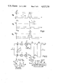
- FIG. 4 shows an embodiment of phase shifter 15 and correlation calculation circuits 19 and 20.
- Phase shifter 15 comprises multiplying circuits 30-33 and combining circuits 34 and 35, which are interconnected such that they can calculate the signals X and Y from the signals x and y and the quantities cos ⁇ VCO and sin ⁇ VCO according to the above formulae (9).
- Correlation calculation circuits 19 and 20 are identical and operate in the same way.
- Circuit 19, for example, comprises a multiplying circuit 36 which forms the product of the samples X produced by phase shifter 15 and samples X' coming from read-only memory 21. These products are accumulated in the accumulator constituted by an adder 37 and memory (MEM.) 38, the result of the accumulation appearing in a buffer memory BUF.
- MEM. memory
- the accumulation is effected at the rate of the clock h at which the samples X and X' appear.
- the accumulator is reset to zero by reset-to-zero signal RAZ 1 , just after the result of the accumulation is sampled in memory 39 by sampling signal H 1 .
- the result of the partial correlations C r (k) appear at the output of memory 39.
- FIG. 5 shows an embodiment of circuit 22 for calculating the error E and circuit 23 for calculating the mean error E m .
- Circuit 22 receives the results of the partial correlations C r (k) and C i (k). It comprises memories 40 and 41 which store the preceding results C r (k-1) and C i (k-1) and, under the control of sampling signal H 1 , recover the correlation results C r (k-1) and C i (k-1) at the same time that the correlation results C r (k) and C i (k) appear. All these correlation results are processed by means of multiplying circuits 42, 43 and combining circuit 44, which are arranged such that they calculate the error signal E according to the above formula (5).
- Mean value calculating circuit 23 comprises an accumulator constituted by an adder 45 and a memory 46, which accumulates the terms of the error E applied to its input under the control of sampling signal H 1 .
- the accumulator is reset to zero by signal RAZ 2 at the end of each step.
- the result of the accumulation is multiplied, just before the accumulator is reset to zero, in a multiplying circuit 47 by the quantity 1/(N m ), N m being the number of the error terms accumulated in each step.
- the result of the multiplying operation is applied to a memory 48, which is read by mean error sampling signal H 2 , in such a way that the mean error terms of each step appear just after the end of each step.
- FIG. 6 shows embodiments of circuits 24 and 25.
- Circuit 24 which has for its object to correct the mean error E m on the basis of the partial correlation results C r (k) and C i (k), comprises squaring circuits 50 and 51 and an adder 52 which are arranged to produce the quantity ##EQU15##
- the quantities ##EQU16## are accumulated in an accumulator constituted by an adder 53 and a memory 54. The accumulation is effected at the rate of partial correlation sampling signal H 1 ; memory 54 is reset to zero by control signal RAZ 2 at the end of each step.
- the output of the accumulator is connected to a circuit 55 which produces the inverse value of the contents of the accumulator; this inverse value is the correction factor C m to be applied to the mean error term E m .
- the factor C m is applied to a buffer memory 56, from which it is read by control signal H 2 and applied to a multiplying circuit 57, to which also the mean error E m is applied which is read from memory 48 by the same control signal H 2 . Circuit 57 thus supplies the corrected error term E*.
- Circuit 25 which has for its object to supply the frequency deviation calculated at the end of each step, comprises, for example, a read-only memory 58 from which the phase deviations ⁇ are read in response to addresses formed by the corrected errors E*.
- the quantities ⁇ T are proportional to the frequency deviations ⁇ f, it is not necessary to calculate these frequency deviations.
- FIG. 7 shows embodiments of circuits 18 and 17.
- Circuit 18 comprises an accumulator which is constituted by an adder 60 and a memory 61 and which, under the control of sampling signal H 3 , accumulates the quantities ⁇ T obtained at the end of the steps of the procedure.
- Memory 61 is reset to zero by signal RAZ 3 at the end of each period T, so that its content is zero at the beginning of the subsequent period.
- the output of accumulator circuit 18 produces the quantity ⁇ VCO ⁇ T which is proportional to the frequency correction f VCO .
- Circuit 17 comprises an accumulator which is constituted by an adder 62 and a memory 63 and accumulates the quantities ⁇ VCO T at the rate of the fast clock h.
- Memory 63 is reset to zero by signal RAZ 4 at the end of each step.
- clock h also provides the reading rate of the samples x and y from memory 12, the output of the accumulator simulates the phase shift ⁇ VCO to which the complex samples of components x and y must be subjected to compensate for the frequency deviation of the local carrier relative to the received carrier.
- the partial correlations for the steps 2, 3, 4 are determined on the basis of the partial correlations calculated during the first step, which also here are formed on the basis of n pairs of samples x and y read from memory 12 and n pairs of samples X' and Y' read from the memory 21.
- n pairs of samples x and y read from memory 12 n pairs of samples X' and Y' read from the memory 21.
- the method used to obtain the partial correlations for the steps 2, 3, 4 consists in adding pair-wise the partial correlations calculated during the respective preceding steps 1, 2, 3. However, before this adding operation is effected, the phase correction of the partial correlations calculated during the preceding phases must first be effected, by using the frequency deviation just estimated.
- FIG. 8 shows how this variation of the method according to the invention can be realized, while for its operation it is possible to use the diagrams already described with reference to FIGS. 3 and 11, in combination with the diagrams 11g, 11h and 11i of FIG. 11.
- FIG. 8 shows how this variation of the method according to the invention can be realized. Elements having the same function as in FIG. 1 are given the same reference numerals in FIG. 8, in which there is shown memory 12 which, as explained above, receives in each period T a pair of samples S r , S i via gates 13 and 14 and has a capacity of n pairs of samples.
- the samples x, y read from memory 12 at the fast clock rate h are directly applied to correlation calculating circuits 19 and 20, simultaneously with the n pairs of samples X', Y' of the local synchronizing word, which are also read at the clock rate h.
- control signals H 1 and RAZ 1 which are identical to the control signals used in the circuit diagram of FIG. 1 and shown in the diagrams 3b and 3e can be used. But actually, in the further course of the schematic diagram, from all partial correlations produced by circuits 19 and 20 only those partial correlations produced during step 1 are used. To that end, the outputs of circuits 19 and 20 are connected to circuit 22 for calculating error E only during step 1 by means of switches 70 and 71 which are set to the suitable position by a control signal H 4 shown in diagram 11g. The outputs of circuits 19 and 20 are also connected to the input of a memory 72 by means of a switch 73 which is also controlled by control signal H 4 such that memory 72 stores the partial correlations processed during step 1.
- the partial correlations produced in the course of step 1 are used to calculate, as explained for the variation of FIG. 1, to calculate the errors E 1 in circuit 22 and thereafter the average error E 1m in circuit 23.
- the 16 partial correlations calculated during step 1 and stored in memory 72 are read therefrom during step 2 by a control signal H 5 , which is shown in diagram 11h.
- These correlations are used in correction circuit 24, which has the same function as correction circuit 24 of FIG. 1, to correct the average error E 1m which also appears during step 2.
- phase shifter 74 produces sequences of phase-corrected partial correlations C x and C y by effecting the calculations:
- phase generator 75 The quantities sin ⁇ ' VCO and cos ⁇ ' VCO are read from read-only memory 16 by means of the phase ⁇ ' VCO produced by a phase generator 75.
- This phase generator is constituted by an accumulator which comprises an adder 76 and a memory 77 and which, at the rate of control signal H 5 , accumulates the phase deviation ⁇ produced by circuit 58 and is reset to zero by signal RAZ 4 at the end of each step.
- the 16 pairs of partial correlations applied during step 2 to phase shifter 74 are phase-corrected therein by the phase ⁇ ' VCO1 obtained by accumulation of the phase deviation ⁇ 1 .
- Each pair of the 16 partial correlations corrected by the phase ⁇ ' VCO1 is applied to adder 78, 79 to be added to the preceding pair of partial correlations which were read from memories 80 and 81 by means of control signal H 5 .
- the sums supplied at the output of circuit 78 and 79 are written into a memory 82 by a control signal H 6 , which is shown in diagram 11i and has a rate which is half the rate of control signal H 5 , such that this memory 82 stores the 8 pairs of partial correlations produced during step 2 starting from the 16 pairs of partial correlations of step 1.
- step 2 These 8 pairs of partial correlations of step 2 are read from memory 82 at the rate of control signal H 6 and are applied on the one hand, via switches 70 and 71, to circuit 22 which calculates the 8 errors E 2 of step 2 and on the other hand, via switch 73, to memory 72 to be stored therein until they are again read from the memory by control signal H 5 in the course of step 3.
- step 3 the procedure already described for step 2 is repeated and the following calculations are effected: the average error E 2m , the corrected error E* 2 , the phase deviation ⁇ 2 , the phase ⁇ ' VCO2 which is used to correct the phase of the 8 partial correlations read from memory 72, and finally the pair-wise sums of the corrected partial correlations are calculated; four of these sums are written into memory 82 and are used in the same way.
- step 4 also the phase deviation ⁇ 3 and the phase ⁇ ' VCO3 are determined which are used to correct the phases of the 4 partial correlations read from memory 72. Finally, during this step 4, two pairs of phase-corrected partial correlations are written into memory 82.
- phase deviation ⁇ 4 may be used to calculate the phase ⁇ ' VCO4 which is used to correct the phases of the two partial correlations read from memory 72 and to form in memory 82 a complete phase-corrected correlation between the local synchronizing word and the received demodulated signal. As has already been described, this complete correlation may be employed for the sampling clock synchronization and the frame synchronization.
- the phases ⁇ ' VCO1 , ⁇ ' VCO2 , ⁇ ' VCO3 , ⁇ ' VCO4 which are used to correct the phases of the partial correlations of each step 1, 2, 3 and 4, are obtained directly from the calculated phase deviations ⁇ 1 , ⁇ 2 , ⁇ 3 , ⁇ 4
- the phases used to correct the samples read from memory 12 are obtained from the accumulated frequency deviations, namely ⁇ f 1 , ⁇ f 1 + ⁇ f 2 , ⁇ f 1 + ⁇ f 2+ ⁇ f 3 , ⁇ f 1 + ⁇ f 2 + ⁇ f 3 + ⁇ f 4 .
- the arrangement of FIG. 8 must be provided with means to process this frequency f VCO .
- the phase deviations ⁇ supplied by circuit 58 are processed in the manner as described with reference to FIGS. 6 and 7.
- the quantities ⁇ T which are proportional to the frequency deviations ⁇ f are accumulated in circuit 18 which supplies at the end of step 4 the quantity ⁇ VCO T which is proportional to the frequency correction f VCO .
- Diagram 9a shows as a function of the time the complete correlation function C, determined in a continuous way, by assuming that clock synchronization has been acquired.
- the correlation function C shows a peak, at one of the sampling clock instants of period T, which are indicated by the graduations of the time axis.
- the function C has the value 1 at the instant t o of this peak and the value -1/n, if, for example, the synchronizing word is a maximum-length sequence.
- the instant t o of the peak indicates the instant at which the n preceding samples of the received signal constitute the transmitted synchronizing word.
- Diagram 9b represents the complete correlation C e determined from the signals sampled with the period T of the sampling clock, as is actually done in the arrangement according to the invention. As it is assumed in diagram 9b that clock synchronization has been acquired, the instant t o of the correlation peak is unambiguously obtained by comparing the correlation C e obtained from the sampled signals to a threshold S e .
- the frequency correction arrangement may be similar, but may process, in time sharing, j signals sampled with the period T and interleaved, to arrive at the end of the frequency correction procedure at j frequency correction values f VCO and finally at j complete correlations which correspond to the said respective j interleaved signals.
- Diagram 9c shows the correlation C es which is the image of the correlation function C of diagram 9a and which is obtained with a sampling frequency 4/T.
- the search procedure for sampling clock synchronization and frame synchronization described in the foregoing can be realized by using the correlation calculation means of the embodiments shown in FIG. 1 and 8.
- the real and imaginary components C i and C r of the complete correlations which can be obtained after the frequency search procedure are, for example, applied to squaring circuits, the squared quantities obtained are applied to an adder forming a sum which is compared to a threshold, the instant at which this threshold is exceeded providing frame synchronization and sampling clock synchronization.
- FIG. 10 a part of the components of FIG. 1 are used and provided with the same reference numerals.
- the bit clock generator 10 has been arranged in the configuration in which it is capable of supplying the frequency 1/% with the phase found at the end of the synchronizing period.
- the samples S r , S i supplied by analog-to-digital converters 8 and 9 at this rate 1/T, are applied directly to a phase shifter which may be the same phase shifter as is used in the frequency correction arrangement according to the invention.
- phase shifter 15 the phases of the samples of the components S r , S i are corrected by using the components sin ⁇ VCO and cos ⁇ VCO read from memory 16 with the aid of the phase ⁇ VCO produced by phase generator 85.
- Phase shifter 15 supplies samples e r , e i which are the result of a calculation operation similar to that indicated by the formulae (9).
- This phase ⁇ VCO is obtained with the aid of an accumulator constituted by an adder 86 and a memory 87.
- the frequency f VCO (or a proportional quantity) stored in memory 88, is accumulated at the accumulation rate 1/T, starting from the initial instant t o determined by a signal RAZ O .
- the corrected samples e r , e i produced by phase shifter 15 are applied to a decision circuit 89 which recovers the data D.
- the frequency f VCO might inter alia be controlled by means of a control loop, which enables the synchronization of the carrier to be maintained and which has no relationship whatsoever with the arrangement according to the invention which is only used to acquire this synchronization.
Landscapes
- Engineering & Computer Science (AREA)
- Computer Networks & Wireless Communication (AREA)
- Signal Processing (AREA)
- Synchronisation In Digital Transmission Systems (AREA)
- Digital Transmission Methods That Use Modulated Carrier Waves (AREA)
Applications Claiming Priority (2)
| Application Number | Priority Date | Filing Date | Title |
|---|---|---|---|
| FR8206289 | 1982-04-09 | ||
| FR8206289A FR2525055A1 (fr) | 1982-04-09 | 1982-04-09 | Procede de correction de frequence de la porteuse locale dans le recepteur d'un systeme de transmission de donnees et recepteur utilisant ce procede |
Publications (1)
| Publication Number | Publication Date |
|---|---|
| US4527278A true US4527278A (en) | 1985-07-02 |
Family
ID=9272965
Family Applications (1)
| Application Number | Title | Priority Date | Filing Date |
|---|---|---|---|
| US06/483,085 Expired - Lifetime US4527278A (en) | 1982-04-09 | 1983-04-07 | Method for correcting the frequency of a local carrier in a receiver of a data transmission system and receiver using this method |
Country Status (8)
Cited By (41)
| Publication number | Priority date | Publication date | Assignee | Title |
|---|---|---|---|---|
| US4613977A (en) * | 1984-01-19 | 1986-09-23 | Standard Telephones And Cables Public Limited Company | Digital Navstar receiver |
| US4796188A (en) * | 1985-10-18 | 1989-01-03 | Stc Plc | Phase rotation of signals |
| US4887050A (en) * | 1989-03-31 | 1989-12-12 | Motorola, Inc. | Frequency control apparatus and method for a digital radio receiver |
| US4943982A (en) * | 1989-05-01 | 1990-07-24 | Motorola, Inc. | Baseband carrier phase corrector |
| US5001727A (en) * | 1989-02-15 | 1991-03-19 | Terra Marine Engineering, Inc. | Carrier and data recovery and demodulation system |
| US5027352A (en) * | 1989-01-05 | 1991-06-25 | Motorola, Inc. | Receiver frequency offset bias circuit for TDM radios |
| US5090028A (en) * | 1989-07-28 | 1992-02-18 | U.S. Philips Corporation | Method of and apparatus for synchronization by means of correlation |
| US5093848A (en) * | 1989-01-26 | 1992-03-03 | Telefonaktiebolaget L M Ericsson | Method of controlling the frequency of a coherent radio receiver and apparatus for carrying out the method |
| US5241702A (en) * | 1990-09-06 | 1993-08-31 | Telefonaktiebolaget L M Ericsson | D.c. offset compensation in a radio receiver |
| US5257291A (en) * | 1990-05-04 | 1993-10-26 | Alcatel N.V. | Circuit for evaluating frequency difference |
| US5297172A (en) * | 1991-04-11 | 1994-03-22 | Comsat Corporation | Method and apparatus for clock recovery for digitally implemented modem |
| US5412693A (en) * | 1992-07-27 | 1995-05-02 | Alcatel Italia S.P.A. | Wholly-digital demodulation system for QAM signalling in low capacity links |
| US5566211A (en) * | 1994-03-25 | 1996-10-15 | Samsung Electronics Co., Ltd. | Automatic frequency control method and apparatus therefor |
| US5579346A (en) * | 1994-01-19 | 1996-11-26 | Kabushiki Kaisha Toshiba | Automatic frequency control method and circuit for use in a delay detection type demodulator |
| US5594758A (en) * | 1992-12-31 | 1997-01-14 | Pacific Communication Sciences, Inc. | Frequency controller and method of correcting phase estimates in a PSK demodulator using frequency control |
| EP1002390A1 (en) * | 1997-08-08 | 2000-05-24 | Arraycomm, Inc. | Method and system for rapid initial signal detection in a wireless communications system |
| GB2344493A (en) * | 1998-09-12 | 2000-06-07 | Roke Manor Research | Automatic frequency correction |
| GB2348786A (en) * | 1999-02-24 | 2000-10-11 | Nec Corp | Compensating for sampling offset using known reference signals |
| WO2001022675A1 (en) * | 1999-09-17 | 2001-03-29 | Cadence Design Systems, Inc. | Estimation of doppler shift in several steps |
| WO2001033794A1 (en) * | 1999-10-29 | 2001-05-10 | Cadence Design Systems, Inc. | Carrier recovery and doppler frequency estimation |
| WO2001049000A1 (en) * | 1999-12-28 | 2001-07-05 | Telefonaktiebolaget Lm Ericsson (Publ) | Method and apparatus for estimating a frequency offset by combining pilot symbols and data symbols |
| GB2358116A (en) * | 1999-02-24 | 2001-07-11 | Nec Corp | Demodulation circuit and method with compensation for sampling offset using known reference signals |
| US6308139B1 (en) * | 1994-06-28 | 2001-10-23 | Siemens Aktiengesellschaft | Digital process for determining the effective value of a periodic electric test signal |
| EP1179901A1 (en) * | 1999-05-18 | 2002-02-13 | Sharp Kabushiki Kaisha | Signal receiver and method of compensating frequency offset |
| US20020175857A1 (en) * | 2001-05-18 | 2002-11-28 | Global Locate Inc. | Method and apparatus for performing signal correlation |
| WO2002096054A1 (en) * | 2001-05-18 | 2002-11-28 | Global Locate, Inc. | Method and apparatus for computing signal correlation |
| US20030219066A1 (en) * | 2001-05-18 | 2003-11-27 | Charles Abraham, Serge De La Porte | Method and apparatus for performing signal correlation |
| US6704348B2 (en) | 2001-05-18 | 2004-03-09 | Global Locate, Inc. | Method and apparatus for computing signal correlation at multiple resolutions |
| US20040086063A1 (en) * | 2002-11-02 | 2004-05-06 | Cho James B. | Apparatus and method for dynamically adjusting receiver bandwidth |
| US6819707B2 (en) | 2001-05-18 | 2004-11-16 | Global Locate, Inc. | Method and apparatus for performing signal correlation using historical correlation data |
| US20050003776A1 (en) * | 2001-11-20 | 2005-01-06 | Katsutoshi Kawai | Radio reception apparatus symbol timing control method, and symbol timing control program |
| US20050080561A1 (en) * | 1999-04-23 | 2005-04-14 | Charles Abraham | Method and apparatus for processing satellite positioning system signals |
| EP1587213A2 (en) * | 2004-04-15 | 2005-10-19 | Fujitsu Limited | Matched filter system |
| US7006556B2 (en) * | 2001-05-18 | 2006-02-28 | Global Locate, Inc. | Method and apparatus for performing signal correlation at multiple resolutions to mitigate multipath interference |
| US20060209935A1 (en) * | 2001-05-18 | 2006-09-21 | Global Locate, Inc. | Method and apparatus for performing signal processing using historical correlation data |
| US20060262835A1 (en) * | 2005-04-25 | 2006-11-23 | Andreas Schmid | Method and device for estimating a frequency in the acquisition of a spread-spectrum code signal |
| US20070025476A1 (en) * | 2005-07-28 | 2007-02-01 | Itt Manufacturing Enterprises, Inc. | Fast digital carrier frequency error estimation algorithm using synchronization sequence |
| WO2007148267A1 (en) * | 2006-06-20 | 2007-12-27 | Nxp B.V. | Method and apparatus for estimating carrier frequency offset |
| US20080112516A1 (en) * | 2001-05-18 | 2008-05-15 | Jason Goldberg | Method and apparatus for providing an energy-based signal tracking loop |
| US7567636B2 (en) | 2001-05-18 | 2009-07-28 | Global Locate, Inc. | Method and apparatus for performing signal correlation using historical correlation data |
| US20100272161A1 (en) * | 2003-10-22 | 2010-10-28 | Jason Goldberg | Method and apparatus for performing frequency synchronization |
Families Citing this family (15)
| Publication number | Priority date | Publication date | Assignee | Title |
|---|---|---|---|---|
| US4563650A (en) * | 1984-01-13 | 1986-01-07 | Westinghouse Electric Corp. | Power line communication receiver with dual threshold signal interrogation capability |
| GB2155268B (en) * | 1984-03-01 | 1987-08-26 | Standard Telephones Cables Ltd | Digital navstar receiver |
| JPH0821962B2 (ja) * | 1984-03-02 | 1996-03-04 | 日本電信電話株式会社 | キヤリアトラツキング回路 |
| US4599732A (en) * | 1984-04-17 | 1986-07-08 | Harris Corporation | Technique for acquiring timing and frequency synchronization for modem utilizing known (non-data) symbols as part of their normal transmitted data format |
| CA1274003A (en) * | 1986-08-21 | 1990-09-11 | Susumu Otani | Carrier recovery circuitry immune to interburst frequency variations |
| GB2203303B (en) * | 1987-03-31 | 1991-02-13 | Stc Plc | Radio frequency tracking loop |
| GB2207582B (en) * | 1987-07-30 | 1991-04-24 | Stc Plc | Phase error correction and carrier recovery |
| FR2633471B1 (fr) * | 1988-06-28 | 1990-10-05 | Trt Telecom Radio Electr | Procede de demodulation coherente d'un signal module numeriquement en phase continue et a enveloppe constante |
| JP2632707B2 (ja) * | 1988-07-30 | 1997-07-23 | 三菱プレシジョン株式会社 | デモジュレーション装置 |
| JP2513331B2 (ja) * | 1989-11-10 | 1996-07-03 | 日本電気株式会社 | 搬送波再生器 |
| DE4013384A1 (de) * | 1990-04-26 | 1991-10-31 | Philips Patentverwaltung | Empfaenger mit einer anordnung zur frequenzablagenschaetzung |
| US5123033A (en) * | 1990-09-27 | 1992-06-16 | At&T Bell Laboratories | Extraction of an exact symbol rate as applied to bandwidth compression of modem signals through demodulation and remodulation |
| CA2079422C (en) * | 1991-09-30 | 1996-07-02 | Osamu Ichiyoshi | Phase-locked circuit capable of being quickly put in a phase-locked state |
| JP3100447B2 (ja) * | 1992-01-10 | 2000-10-16 | 三菱電機株式会社 | 適応等化器および受信機 |
| JPH0951295A (ja) * | 1995-08-04 | 1997-02-18 | Matsushita Electric Ind Co Ltd | データ受信装置 |
Citations (5)
| Publication number | Priority date | Publication date | Assignee | Title |
|---|---|---|---|---|
| US3447085A (en) * | 1965-01-04 | 1969-05-27 | Gen Dynamics Corp | Synchronization of receiver time base in plural frequency differential phase shift system |
| US3961262A (en) * | 1973-11-22 | 1976-06-01 | International Standard Electric Corporation | FM receiver and demodulation circuit |
| US4213006A (en) * | 1976-12-21 | 1980-07-15 | Siemens Aktiengesellschaft | Circuit arrangement for the coarse synchronization of carrier signals and pulse signals with data signals in a data receiver |
| US4313219A (en) * | 1979-04-02 | 1982-01-26 | Siemens Aktiengesellschaft | Receiver for high frequency electromagnetic oscillations having a frequency readjustment |
| US4328587A (en) * | 1979-02-19 | 1982-05-04 | Kokusai Denshin Denwa Kabushiki Kaisha | Phase slip detector and systems employing the detector |
Family Cites Families (3)
| Publication number | Priority date | Publication date | Assignee | Title |
|---|---|---|---|---|
| US3971996A (en) * | 1973-01-18 | 1976-07-27 | Hycom Incorporated | Phase tracking network |
| US3962637A (en) * | 1974-11-11 | 1976-06-08 | Hycom Incorporated | Ultrafast adaptive digital modem |
| DE2608258C2 (de) * | 1976-02-28 | 1984-04-05 | Licentia Patent-Verwaltungs-Gmbh, 6000 Frankfurt | Einseitenband- oder Zweiseitenband- Nachrichtenübertragungsverfahren ohne Träger |
-
1982
- 1982-04-09 FR FR8206289A patent/FR2525055A1/fr active Granted
-
1983
- 1983-03-31 EP EP83200461A patent/EP0091167B1/fr not_active Expired
- 1983-03-31 DE DE8383200461T patent/DE3361666D1/de not_active Expired
- 1983-04-06 NO NO831221A patent/NO831221L/no unknown
- 1983-04-06 CA CA000425288A patent/CA1211794A/en not_active Expired
- 1983-04-06 AU AU13173/83A patent/AU556701B2/en not_active Ceased
- 1983-04-07 US US06/483,085 patent/US4527278A/en not_active Expired - Lifetime
- 1983-04-09 JP JP58061574A patent/JPH0638611B2/ja not_active Expired - Lifetime
Patent Citations (5)
| Publication number | Priority date | Publication date | Assignee | Title |
|---|---|---|---|---|
| US3447085A (en) * | 1965-01-04 | 1969-05-27 | Gen Dynamics Corp | Synchronization of receiver time base in plural frequency differential phase shift system |
| US3961262A (en) * | 1973-11-22 | 1976-06-01 | International Standard Electric Corporation | FM receiver and demodulation circuit |
| US4213006A (en) * | 1976-12-21 | 1980-07-15 | Siemens Aktiengesellschaft | Circuit arrangement for the coarse synchronization of carrier signals and pulse signals with data signals in a data receiver |
| US4328587A (en) * | 1979-02-19 | 1982-05-04 | Kokusai Denshin Denwa Kabushiki Kaisha | Phase slip detector and systems employing the detector |
| US4313219A (en) * | 1979-04-02 | 1982-01-26 | Siemens Aktiengesellschaft | Receiver for high frequency electromagnetic oscillations having a frequency readjustment |
Cited By (78)
| Publication number | Priority date | Publication date | Assignee | Title |
|---|---|---|---|---|
| US4613977A (en) * | 1984-01-19 | 1986-09-23 | Standard Telephones And Cables Public Limited Company | Digital Navstar receiver |
| US4796188A (en) * | 1985-10-18 | 1989-01-03 | Stc Plc | Phase rotation of signals |
| US5027352A (en) * | 1989-01-05 | 1991-06-25 | Motorola, Inc. | Receiver frequency offset bias circuit for TDM radios |
| US5093848A (en) * | 1989-01-26 | 1992-03-03 | Telefonaktiebolaget L M Ericsson | Method of controlling the frequency of a coherent radio receiver and apparatus for carrying out the method |
| US5001727A (en) * | 1989-02-15 | 1991-03-19 | Terra Marine Engineering, Inc. | Carrier and data recovery and demodulation system |
| US4887050A (en) * | 1989-03-31 | 1989-12-12 | Motorola, Inc. | Frequency control apparatus and method for a digital radio receiver |
| US4943982A (en) * | 1989-05-01 | 1990-07-24 | Motorola, Inc. | Baseband carrier phase corrector |
| US5090028A (en) * | 1989-07-28 | 1992-02-18 | U.S. Philips Corporation | Method of and apparatus for synchronization by means of correlation |
| US5257291A (en) * | 1990-05-04 | 1993-10-26 | Alcatel N.V. | Circuit for evaluating frequency difference |
| US5241702A (en) * | 1990-09-06 | 1993-08-31 | Telefonaktiebolaget L M Ericsson | D.c. offset compensation in a radio receiver |
| US5297172A (en) * | 1991-04-11 | 1994-03-22 | Comsat Corporation | Method and apparatus for clock recovery for digitally implemented modem |
| US5412693A (en) * | 1992-07-27 | 1995-05-02 | Alcatel Italia S.P.A. | Wholly-digital demodulation system for QAM signalling in low capacity links |
| US5594758A (en) * | 1992-12-31 | 1997-01-14 | Pacific Communication Sciences, Inc. | Frequency controller and method of correcting phase estimates in a PSK demodulator using frequency control |
| US5579346A (en) * | 1994-01-19 | 1996-11-26 | Kabushiki Kaisha Toshiba | Automatic frequency control method and circuit for use in a delay detection type demodulator |
| US5566211A (en) * | 1994-03-25 | 1996-10-15 | Samsung Electronics Co., Ltd. | Automatic frequency control method and apparatus therefor |
| US6308139B1 (en) * | 1994-06-28 | 2001-10-23 | Siemens Aktiengesellschaft | Digital process for determining the effective value of a periodic electric test signal |
| EP1002390A1 (en) * | 1997-08-08 | 2000-05-24 | Arraycomm, Inc. | Method and system for rapid initial signal detection in a wireless communications system |
| EP1002390A4 (en) * | 1997-08-08 | 2002-10-09 | Arraycomm Inc | METHOD AND DEVICE FOR FAST DETECTING SIGNALS IN A WIRELESS MESSAGE TRANSMISSION SYSTEM |
| GB2344493A (en) * | 1998-09-12 | 2000-06-07 | Roke Manor Research | Automatic frequency correction |
| GB2358116B (en) * | 1999-02-24 | 2002-11-06 | Nec Corp | Demodulation circuit and demodulation method with compensation for sampling offset |
| GB2358116A (en) * | 1999-02-24 | 2001-07-11 | Nec Corp | Demodulation circuit and method with compensation for sampling offset using known reference signals |
| US20050190847A1 (en) * | 1999-02-24 | 2005-09-01 | Nec Corporation | Demodulation and modulation circuit and demodulation and modulation method |
| GB2348786B (en) * | 1999-02-24 | 2002-02-13 | Nec Corp | Demodulation circuit and demodulation method with compensation for sampling offset |
| US7110476B1 (en) | 1999-02-24 | 2006-09-19 | Nec Corporation | Demodulation and modulation circuit and demodulation and modulation method |
| GB2348786A (en) * | 1999-02-24 | 2000-10-11 | Nec Corp | Compensating for sampling offset using known reference signals |
| US9020756B2 (en) | 1999-04-23 | 2015-04-28 | Global Locate, Inc. | Method and apparatus for processing satellite positioning system signals |
| US20090153399A1 (en) * | 1999-04-23 | 2009-06-18 | Charles Abraham | Method and apparatus for processing satellite positioning system signals |
| US20050080561A1 (en) * | 1999-04-23 | 2005-04-14 | Charles Abraham | Method and apparatus for processing satellite positioning system signals |
| EP1179901A1 (en) * | 1999-05-18 | 2002-02-13 | Sharp Kabushiki Kaisha | Signal receiver and method of compensating frequency offset |
| EP1179901A4 (en) * | 1999-05-18 | 2003-03-19 | Sharp Kk | SIGNAL RECEIVER AND FREQUENCY OFFSET COMPENSATION METHOD |
| US7149266B1 (en) | 1999-05-18 | 2006-12-12 | Sharp Kabushiki Kaisha | Signal receiver and method of compensating frequency offset |
| WO2001022675A1 (en) * | 1999-09-17 | 2001-03-29 | Cadence Design Systems, Inc. | Estimation of doppler shift in several steps |
| US6426982B1 (en) | 1999-09-17 | 2002-07-30 | Cadonca Design Systems, Inc. | Low complexity multiple bits matched filter |
| US6532271B1 (en) | 1999-10-29 | 2003-03-11 | Cadence Design Systems, Inc. | Carrier recovery and doppler frequency estimation |
| WO2001033794A1 (en) * | 1999-10-29 | 2001-05-10 | Cadence Design Systems, Inc. | Carrier recovery and doppler frequency estimation |
| US6606363B1 (en) | 1999-12-28 | 2003-08-12 | Telefonaktiebolaget Lm Ericsson (Publ) | Method and apparatus for estimating a frequency offset by combining pilot symbols and data symbols |
| WO2001049000A1 (en) * | 1999-12-28 | 2001-07-05 | Telefonaktiebolaget Lm Ericsson (Publ) | Method and apparatus for estimating a frequency offset by combining pilot symbols and data symbols |
| US20080112516A1 (en) * | 2001-05-18 | 2008-05-15 | Jason Goldberg | Method and apparatus for providing an energy-based signal tracking loop |
| US6606346B2 (en) * | 2001-05-18 | 2003-08-12 | Global Locate, Inc. | Method and apparatus for computing signal correlation |
| US20020175857A1 (en) * | 2001-05-18 | 2002-11-28 | Global Locate Inc. | Method and apparatus for performing signal correlation |
| US8411726B2 (en) | 2001-05-18 | 2013-04-02 | Global Locate, Inc. | Method and apparatus for performing signal correlation at multiple resolutions to mitigate multipath interference |
| US6891880B2 (en) | 2001-05-18 | 2005-05-10 | Global Locate, Inc. | Method and apparatus for performing signal correlation |
| US8170086B2 (en) | 2001-05-18 | 2012-05-01 | Global Locate, Inc. | Method and apparatus for performing signal correlation |
| US8098716B2 (en) | 2001-05-18 | 2012-01-17 | Broadcom Corporation | Method and apparatus for providing an energy-based signal tracking loop |
| US8005174B2 (en) | 2001-05-18 | 2011-08-23 | Broadcom Corporation | Method and apparatus for performing signal correlation using historical correlation data |
| US7995682B2 (en) | 2001-05-18 | 2011-08-09 | Broadcom Corporation | Method and apparatus for performing signal processing using historical correlation data |
| US7006556B2 (en) * | 2001-05-18 | 2006-02-28 | Global Locate, Inc. | Method and apparatus for performing signal correlation at multiple resolutions to mitigate multipath interference |
| US20060114970A1 (en) * | 2001-05-18 | 2006-06-01 | Global Locate, Inc. | Method and apparatus for performing signal correlation at multiple resolutions to mitigate multipath interference |
| US6704348B2 (en) | 2001-05-18 | 2004-03-09 | Global Locate, Inc. | Method and apparatus for computing signal correlation at multiple resolutions |
| US20060209935A1 (en) * | 2001-05-18 | 2006-09-21 | Global Locate, Inc. | Method and apparatus for performing signal processing using historical correlation data |
| US20100098136A1 (en) * | 2001-05-18 | 2010-04-22 | Charles Abraham | Method and apparatus for performing signal correlation at multiple resolutions to mitigate multipath interference |
| US20030219066A1 (en) * | 2001-05-18 | 2003-11-27 | Charles Abraham, Serge De La Porte | Method and apparatus for performing signal correlation |
| US7672358B2 (en) | 2001-05-18 | 2010-03-02 | Broadcom Corporation | Method and apparatus for performing signal correlation at multiple resolutions to mitigate multipath interference |
| US20090262789A1 (en) * | 2001-05-18 | 2009-10-22 | Charles Abraham | Method and apparatus for performing signal correlation using historical correlation data |
| US7184464B2 (en) | 2001-05-18 | 2007-02-27 | Global Locate, Inc | Apparatus for computing signal correlation at multiple resolutions |
| US7190712B2 (en) | 2001-05-18 | 2007-03-13 | Global Locate, Inc | Method and apparatus for performing signal correlation |
| US20070160121A1 (en) * | 2001-05-18 | 2007-07-12 | Global Locate, Inc. | Method and apparatus for performing signal correlation |
| US7567636B2 (en) | 2001-05-18 | 2009-07-28 | Global Locate, Inc. | Method and apparatus for performing signal correlation using historical correlation data |
| US6819707B2 (en) | 2001-05-18 | 2004-11-16 | Global Locate, Inc. | Method and apparatus for performing signal correlation using historical correlation data |
| WO2002096054A1 (en) * | 2001-05-18 | 2002-11-28 | Global Locate, Inc. | Method and apparatus for computing signal correlation |
| US20050003776A1 (en) * | 2001-11-20 | 2005-01-06 | Katsutoshi Kawai | Radio reception apparatus symbol timing control method, and symbol timing control program |
| US7149491B2 (en) | 2001-11-20 | 2006-12-12 | Sanyo Electric Co., Ltd. | Radio reception apparatus symbol timing control method, and symbol timing control program |
| US20040086063A1 (en) * | 2002-11-02 | 2004-05-06 | Cho James B. | Apparatus and method for dynamically adjusting receiver bandwidth |
| US7443935B2 (en) * | 2002-11-02 | 2008-10-28 | Texas Instruments Incorporated | Apparatus and method for dynamically adjusting receiver bandwidth |
| WO2004086077A1 (en) * | 2003-03-21 | 2004-10-07 | Global Locate Inc. | Method and apparatus for performing signal correlation |
| US8989236B2 (en) | 2003-10-22 | 2015-03-24 | Global Locate, Inc. | Method and apparatus for performing frequency synchronization |
| US8472503B2 (en) | 2003-10-22 | 2013-06-25 | Global Locate, Inc. | Method and apparatus for performing frequency synchronization |
| US20100272161A1 (en) * | 2003-10-22 | 2010-10-28 | Jason Goldberg | Method and apparatus for performing frequency synchronization |
| EP1587213A2 (en) * | 2004-04-15 | 2005-10-19 | Fujitsu Limited | Matched filter system |
| EP1587213A3 (en) * | 2004-04-15 | 2005-11-16 | Fujitsu Limited | Matched filter system |
| US20050232343A1 (en) * | 2004-04-15 | 2005-10-20 | Kazuhiko Sakai | Matched filter system |
| US7839918B2 (en) * | 2005-04-25 | 2010-11-23 | Infineon Technologies Ag | Method and device for estimating a frequency in the acquisition of a spread-spectrum code signal |
| US20060262835A1 (en) * | 2005-04-25 | 2006-11-23 | Andreas Schmid | Method and device for estimating a frequency in the acquisition of a spread-spectrum code signal |
| US7630428B2 (en) * | 2005-07-28 | 2009-12-08 | Itt Manufacturing Enterprises, Inc. | Fast digital carrier frequency error estimation algorithm using synchronization sequence |
| US20070025476A1 (en) * | 2005-07-28 | 2007-02-01 | Itt Manufacturing Enterprises, Inc. | Fast digital carrier frequency error estimation algorithm using synchronization sequence |
| US8446938B2 (en) | 2006-06-20 | 2013-05-21 | Nxp B.V. | Method and apparatus for estimating carrier frequency offset |
| US20090274250A1 (en) * | 2006-06-20 | 2009-11-05 | Nxp B.V. | Method and apparatus for estimating carrier frequency offset |
| WO2007148267A1 (en) * | 2006-06-20 | 2007-12-27 | Nxp B.V. | Method and apparatus for estimating carrier frequency offset |
Also Published As
| Publication number | Publication date |
|---|---|
| CA1211794A (en) | 1986-09-23 |
| FR2525055B1 (US06826419-20041130-M00005.png) | 1984-05-04 |
| AU556701B2 (en) | 1986-11-13 |
| JPS58187046A (ja) | 1983-11-01 |
| DE3361666D1 (en) | 1986-02-13 |
| NO831221L (no) | 1983-10-10 |
| JPH0638611B2 (ja) | 1994-05-18 |
| FR2525055A1 (fr) | 1983-10-14 |
| EP0091167A1 (fr) | 1983-10-12 |
| AU1317383A (en) | 1983-10-13 |
| EP0091167B1 (fr) | 1986-01-02 |
Similar Documents
| Publication | Publication Date | Title |
|---|---|---|
| US4527278A (en) | Method for correcting the frequency of a local carrier in a receiver of a data transmission system and receiver using this method | |
| US5946359A (en) | Parameter measuring apparatus for digital quadrature modulation signals | |
| US5590158A (en) | Method and apparatus for estimating PSK modulated signals | |
| US5276710A (en) | Carrier frequency error detector capable of accurately detecting a carrier frequency error | |
| US4879728A (en) | DPSK carrier acquisition and tracking arrangement | |
| US5343497A (en) | Method and device for the synchronization between a base radio station and a mobile radio station in a digital radiomobile system | |
| US4689806A (en) | Receiver mode control for acquiring and tracking a signal | |
| US5475705A (en) | Demodulator for Manchester-coded FM signals | |
| AU643296B2 (en) | Clock recovery circuit with open-loop phase estimator and wideband phase tracking loop | |
| CN112840611B (zh) | 使用多个数字解调器解调数字信号的方法 | |
| US4516079A (en) | Coherent phase shift keyed demodulator for power line communication systems | |
| US4042884A (en) | Phase demodulator with offset frequency reference oscillator | |
| US4794624A (en) | Method for clock synchronization of a signal receiver | |
| US5867059A (en) | Demodulating system for MSK and GMSK signal using a fast fourier transform converter | |
| EP0259867A2 (en) | Demodulator for psk-modulated signals | |
| CA2318988C (en) | Receiver | |
| JP3890867B2 (ja) | 受信機および送受信機 | |
| EP0881798A1 (en) | Method and device for recovering synchronization on a signal transmitted to a mobile-telephone receiver | |
| JP2000115269A (ja) | キャリア位相追従装置および周波数ホッピング受信装置 | |
| EP0783214A2 (en) | Data synchronizer phase detector and method of operation thereof | |
| JP2931454B2 (ja) | ディジタル位相変調信号復調回路 | |
| JPH1056486A (ja) | 復調装置 | |
| JP2540931B2 (ja) | Psk信号復調方法 | |
| JPS6353745B2 (US06826419-20041130-M00005.png) | ||
| JP2698979B2 (ja) | Psk復調器における搬送波再生方式 |
Legal Events
| Date | Code | Title | Description |
|---|---|---|---|
| AS | Assignment |
Owner name: U.S. PHILIPS CORPOATION, 100 EAST 42ND ST., NEW YO Free format text: ASSIGNMENT OF ASSIGNORS INTEREST.;ASSIGNORS:DECONCHE, ALAIN;VAN UFFELEN, JEAN-PIERRE H.;REEL/FRAME:004130/0021 Effective date: 19830419 Owner name: U.S. PHILIPS CORPOATION, 100 EAST 42ND ST., NEW YO Free format text: ASSIGNMENT OF ASSIGNORS INTEREST;ASSIGNORS:DECONCHE, ALAIN;VAN UFFELEN, JEAN-PIERRE H.;REEL/FRAME:004130/0021 Effective date: 19830419 |
|
| STCF | Information on status: patent grant |
Free format text: PATENTED CASE |
|
| CC | Certificate of correction | ||
| FEPP | Fee payment procedure |
Free format text: PAYOR NUMBER ASSIGNED (ORIGINAL EVENT CODE: ASPN); ENTITY STATUS OF PATENT OWNER: LARGE ENTITY |
|
| FPAY | Fee payment |
Year of fee payment: 4 |
|
| FPAY | Fee payment |
Year of fee payment: 8 |
|
| FPAY | Fee payment |
Year of fee payment: 12 |