US4261056A - Equalizing signal combiner - Google Patents
Equalizing signal combiner Download PDFInfo
- Publication number
- US4261056A US4261056A US06/057,748 US5774879A US4261056A US 4261056 A US4261056 A US 4261056A US 5774879 A US5774879 A US 5774879A US 4261056 A US4261056 A US 4261056A
- Authority
- US
- United States
- Prior art keywords
- signal
- auxiliary
- equalizing
- combiner
- frequency
- Prior art date
- Legal status (The legal status is an assumption and is not a legal conclusion. Google has not performed a legal analysis and makes no representation as to the accuracy of the status listed.)
- Expired - Lifetime
Links
Images


Classifications
-
- H—ELECTRICITY
- H04—ELECTRIC COMMUNICATION TECHNIQUE
- H04B—TRANSMISSION
- H04B7/00—Radio transmission systems, i.e. using radiation field
- H04B7/02—Diversity systems; Multi-antenna system, i.e. transmission or reception using multiple antennas
- H04B7/04—Diversity systems; Multi-antenna system, i.e. transmission or reception using multiple antennas using two or more spaced independent antennas
- H04B7/08—Diversity systems; Multi-antenna system, i.e. transmission or reception using multiple antennas using two or more spaced independent antennas at the receiving station
- H04B7/0837—Diversity systems; Multi-antenna system, i.e. transmission or reception using multiple antennas using two or more spaced independent antennas at the receiving station using pre-detection combining
- H04B7/084—Equal gain combining, only phase adjustments
-
- H—ELECTRICITY
- H04—ELECTRIC COMMUNICATION TECHNIQUE
- H04B—TRANSMISSION
- H04B7/00—Radio transmission systems, i.e. using radiation field
- H04B7/02—Diversity systems; Multi-antenna system, i.e. transmission or reception using multiple antennas
- H04B7/04—Diversity systems; Multi-antenna system, i.e. transmission or reception using multiple antennas using two or more spaced independent antennas
- H04B7/08—Diversity systems; Multi-antenna system, i.e. transmission or reception using multiple antennas using two or more spaced independent antennas at the receiving station
- H04B7/0837—Diversity systems; Multi-antenna system, i.e. transmission or reception using multiple antennas using two or more spaced independent antennas at the receiving station using pre-detection combining
- H04B7/0842—Weighted combining
- H04B7/0848—Joint weighting
- H04B7/0851—Joint weighting using training sequences or error signal
-
- H—ELECTRICITY
- H04—ELECTRIC COMMUNICATION TECHNIQUE
- H04B—TRANSMISSION
- H04B7/00—Radio transmission systems, i.e. using radiation field
- H04B7/02—Diversity systems; Multi-antenna system, i.e. transmission or reception using multiple antennas
- H04B7/04—Diversity systems; Multi-antenna system, i.e. transmission or reception using multiple antennas using two or more spaced independent antennas
- H04B7/08—Diversity systems; Multi-antenna system, i.e. transmission or reception using multiple antennas using two or more spaced independent antennas at the receiving station
- H04B7/0837—Diversity systems; Multi-antenna system, i.e. transmission or reception using multiple antennas using two or more spaced independent antennas at the receiving station using pre-detection combining
- H04B7/0842—Weighted combining
- H04B7/0848—Joint weighting
- H04B7/0857—Joint weighting using maximum ratio combining techniques, e.g. signal-to- interference ratio [SIR], received signal strenght indication [RSS]
Definitions
- This invention relates to space diversity receivers and, in particular, to circuit arrangements for combining the two signals received in such systems.
- blind switching it is assumed that the signal received by the second antenna is stronger than that received by the first antenna.
- the signals from the two antennas are combined at radio frequency or at an intermediate frequency instead of switching between the two. This eliminates amplitude and phase jumps associated with the switching operation, and has the added advantage of delivering a larger amplitude signal to the receiver.
- the situation is more complex in a digital radio system.
- bit error rate (BER) in a digital system is more sensitive to the degree of inband amplitude dispersion and less sensitive to the magnitude of a flat fade.
- Nippon Electric Company includes in their Model RP-6G178MB, 78Mb/s, 6GHz, 8PSK system an equalizer following their maximum power signal combiner.
- the Collins Radio Division of Rockwell International provides in their Model MDR-6 radio system two separate, equalized receivers and switches between them at baseband as signal conditions require.
- the broad objective of the present invention is to simplify space diversity receivers used in digital radio systems.
- a signal combiner in accordance with the invention trades off output power in favor of reduced amplitude dispersion by measuring the powers within selected portions of the output signal and varying the circuit parameters in a manner to maintain any preselected relationship among the measured powers.
- the signals are combined at IF and the relative amplitudes of selected frequency components in the combined signal are measured.
- a control signal is generated which changes the relative phase of the local oscillator signals coupled to the frequency down-converters in the receiver input circuits.
- the control signal can be designed to establish and maintain any preselected relationship among the measured frequency components.
- the total power in the combined signal is also monitored, and the control signal biased to take onto account very deep fades.
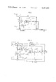
- FIG. 1 shows, in block diagram, the elements of an equalizing combiner in accordance with the present invention
- FIG. 2 shows a second embodiment of the invention
- FIG. 3 shows an illustrative embodiment of a phase shifter
- FIGS. 4, 5 and 6 are included for purposes of explaining the operation of the phase shifter of FIG. 3;
- FIG. 7 shows an illustrative embodiment of a sensor and control signal generator
- FIG. 8 shows an alternate embodiment of the invention.
- FIG. 1 shows, in block diagram, the elements of an equalizing combiner in accordance with the present invention.
- the combiner comprises a pair of signal circuits 10 and 11, each of which includes an antenna 12, 13 and a frequency converter 14, 15.
- a common local oscillator 16 provides local oscillator signals for the converters at a relative phase determined by a phase shifter 17 included between oscillator 16 and one of the converters 14.
- the resulting intermediate frequency signals, produced by the converters, are combined in a common output circuit by means of a coupler 18.
- a combiner in accordance with the present invention monitors the power in selected frequency components of the combined output signal in addition to the total output power. This is done in a sensor 19 connected to the output port of coupler 18. The results of these measurements are evaluated by a control signal generator 20, in accordance with whatever criteria have been preselected, and a control signal generated which varies the phase shift produced by phase shifter 17.
- converters 14 and 15 down convert the inputs from the two spaced diversity antennas, adding a phase shift, ⁇ , to one of them.
- the resulting IF signals are then added vectorially in coupler 18 to produce an output signal whose envelope is given by
- v 1 (t) and v 2 (t) are the envelopes of the input signals.
- Sensor 19 monitors, at the combined output, the channel loss and the amplitude difference between components at two fixed frequencies within the band of interest. This information provides the data from which the control signal is generated.
- K( ⁇ ) For purposes of illustration, let us define a control function K( ⁇ ) given by
- the amplitude difference is in dB; the channel loss is in dB relative to an unfaded signal; and
- ⁇ , ⁇ and ⁇ are constants.
- FIG. 2 shows a second embodiment of an equalizing combiner in accordance with the invention.
- the combiner comprises a main signal circuit, including substantially the same components as in FIG. 1, and a substantially similar auxiliary circuit to which the sensor and control generator are connected.
- the main circuit comprises: a first wavepath 10 including a first antenna 12, a first hybrid coupler 21, and a first frequency converter 14; and a second wavepath 11 including a second antenna 13, a second frequency converter 15, and a second hybrid coupler 23.
- a local oscillator 16 is coupled to each converter by means including, in one path, phase shifter 17.
- the IF signals in wavepaths 10 and 11 are combined in a common output by main signal output coupler 18.
- the auxiliary circuit includes a first auxiliary branch 5 connected to first coupler 21 for coupling a portion of the RF signal in wavepath 10 to a first auxiliary frequency converter 22.
- a second auxiliary branch 6 connected to second coupler 23 couples a component of the IF signal out of wavepath 11. The latter component and the output from converter 22 are added together by means of an auxiliary output coupler 25.
- Frequency conversion in converter 22 is affected with a component of local oscillator signal from oscillator 16 which is coupled through phase shifter 17 and an auxiliary phase modulator 26.
- the phase shift, ⁇ , through the latter is slowly modulated at a frequency f c , of the order of 1000 Hz, in response to a second local oscillator 27.
- the latter is also coupled to generator 20. The reason for this will become apparent hereinbelow.
- the combined output signal from coupler 25 is coupled to sensor 19, wherein the appropriate signals are sampled.
- the sensor outputs are coupled, in turn, to control signal generator 20 wherein the appropriate control signal is generated for varying the phase shift through phase shifter 17.
- control signal is generated within an auxiliary combiner circuit that reflects, at any instant, the operating conditions that the main combiner circuit would have if its phase were offset by ⁇ .
- the combined auxiliary signal v c '(t) at the output of coupler 25 may be expressed as
- the auxiliary circuit is aligned by adjusting the coupler ratios such that
- a and b are the coefficients of equation (1).
- control signal K( ⁇ ) is developed from the auxiliary combiner output signal v c '(t) and, as noted, is a function of the average power within the channel and the power within two narrow portions of the channel centered about selected frequencies f 1 and f 2 . Typically, these would be located near the 3 dB points of the spectrum of the received signal. Because of the phase modulations ⁇ , however, one obtains from these measurements, a control signal K( ⁇ + ⁇ ) which includes a component K( ⁇ ) and a component K 1 ( ⁇ ) ⁇ which indicates the direction in which ⁇ should change in order to reduce the magnitude of K( ⁇ ). If, for example, K( ⁇ + ⁇ ) increases when ⁇ increases, ⁇ should be decreased.
- FIGS. 3, 4, 5, 6 and 7, included for purposes of explanation, show illustrative embodiments of a phase shifter, sensor, and a control signal generator for use with the present invention.
- phase shifter 17 in response to a signal from the control generator, provides a continuously variable phase shift for the local oscillator signal coupled to frequency converter 14.
- a variable phase shift is obtained by varying the relative amplitudes and polarities of two orthogonal signal components.
- the signal V from oscillator 16 is coupled by means of two wavepaths 8 and 9 to a summing amplifier 38.
- One wavepath 8 includes a variable gain amplifier 31 and a 90 degree phase shifter 30.
- the other wavepath 9 includes a second variable gain amplifier 32 that is substantially identical to amplifier 31.
- the local oscillator input signal, V applied to the phase shifter produces output signals V' and V" at summing amplifier 38, as illustrated in FIG. 4.
- the phase of the output signal V 01 from amplifier 38 which is the vector sum of these two input signals, will depend upon their relative amplitudes and polarities. As illustrated in FIG. 4, output V 01 is in the first quadrant. If, on the other hand, the sense of signal V" is reversed, as in FIG. 5, the phase of V 01 will increase to some value in the second quadrant.
- Control of the amplitudes and polarities of signal components V" and V' is provided by the bias voltages V 31 and V 32 applied to amplifiers 31 and 32, respectively.
- the bias voltage circuits for generating these voltages include the variable gain amplifiers 33 and 35, integrating circuits 34 and 36, and inverter 37.
- a control signal V e from the control signal generator is coupled to each of the amplifiers 33 and 35.
- the resulting output signals are coupled, respectively, to integrators 34 and 36.
- the output V 31 from integrator 34 controls the gain of amplifier 31 and, in addition, is cross-coupled, through inverter 37, to amplifier 35 for controlling the gain of the latter.
- the output from integrator 36 is coupled to amplifiers 32 and 33 for controlling their gains.
- Each of the amplifiers 31, 32, 33 and 35 has a gain-bias characteristic of the type shown in FIG. 6. Thus, a positive bias signal produces an output signal having the same polarity as the input signal, whereas a negative bias voltage produces an output signal having the opposite polarity.
- phase shift ⁇ 2 is initially zero.
- V 31 is initially zero (i.e., zero gain in amplifier 31)
- V 32 is a positive voltage (i.e., positive gain through amplifier 32).
- V e If V e remains applied, the output from integrator 36 will, in time, become negative, causing first V" to reverse phase and then V' to reverse phase, thereby rotating the vector sum V 01 through the remaining three phase quadrants.
- the amplitude and sense of the control signal V e will vary as a function of the phase shift through phase shifter 17, and only limited phase shift corrections will be made to equalize the inband dispersion.
- the limiter 39 and filter 29 are included merely to maintain a constant output signal and can alternatively be replaced by an amplifier with automatic gain control.
- one object of the sensor is to measure the power difference in dB in two selected portions of the channel so as to obtain an indication of the inband amplitude dispersion.
- the power in the band portion centered at f 1 is obtained by applying signal v c '(t) to a bandpass filter 40, detecting the output in a square law detector 42, and then filtering the detected signal in a lowpass filter 44. The resulting signal is converted to dB by log amplifier 46.
- the power in the hand portion centered at frequency f 2 is obtained by means of bandpass filter 41, square law detector 43, lowpass filter 45, and log amplifier 47.
- the outputs from amplifiers 46 and 47 are coupled to difference amplifier 48 in the control signal generator 20.
- the output of amplifier 48 is coupled to an amplitude detector 49.
- the first weighted term, (amplitude difference).sup. ⁇ , of equation (2) is then formed by log amplifier 50, amplifier 51 and antilog amplifier 52.
- a second object of the sensor is to measure the total inband power. This is accomplished by channel filter 53, square law detector 54, lowpass filter 55, and log amplifier 56. This signal is then compared with a reference level signal in a difference amplifier 57 in the control signal generator, where the reference level signal is indicative of an unfaded signal. This measurement is weighted by means of amplifier 58, log amplifier 59, amplifier 60, and antilog amplifier 61 to form the second term, ( ⁇ channel loss).sup. ⁇ , of equation (2).
- the two terms are then combined in a summing amplifier 62 to form the signal K( ⁇ + ⁇ ).
- the signal K( ⁇ + ⁇ ) is compared with the phase modulating signal from oscillator 27 in a phase detector 63.
- control signal generator has been described using analog devices, it is apparent that the signals from the sensor can be digitized and the control signal generator implemented using digital techniques.
- FIG. 8 shows an alternate embodiment of the invention wherein the combiner operates on the signals after they have been converted to their IF freqency.
- the main signal circuit includes wavepaths 80, 81 and output coupler 84.
- Wavepath 80 includes a first hybrid coupler 82, and first and second frequency converters 85 and 86.
- Wavepath 81 includes a second hybrid coupler 83.
- the auxiliary circuit comprises branches 70 and 71.
- the first branch 70 connected between hybrid coupler 82 and auxiliary output coupler 94, includes first and second auxiliary frequency converters 88 and 89.
- the second auxiliary branch is connected between hybrid coupler 83 and output coupler 94.
- a local oscillator 87 is connected directly to each of the converters 86 and 89, and to converters 85 and 88 through phase shifters 90 and 90 and 92, respectively.
- a second local oscillator 93 is coupled to phase shifter 92 and to control signal generator 98. Also coupled to control signal generator 98 are the output signals from sensor 95 which senses the power in selected portions of the output signal from coupler 94.
- the IF signal in wavepath 81 is coupled directly to output coupler 84.
- the IF signal in wavepath 80 undergoes a frequency conversion in converter 85 (either up or down) to a second IF frequency followed by another frequency conversion in converter 86 back to the original IF frequency. Because of the relative phase shift ⁇ between the phases of the local oscillator signals coupled to converters 85 and 86, the resulting IF signal components in wavepath 80 experience an added phase shift relative to the signal in wavepath 81.
- the signal components in the first auxiliary branch experience the same phase shift relative to the signal components in the second auxiliary branch, except that there is the added phase shift ⁇ induced in phase shifter 92 by the second local oscillator 93.
- the output signal v c (t) from output coupler 84 and v c '(t) from auxiliary output coupler 94 are the same as those produced in the embodiment of FIG. 2 and, hence, equalization is achieved in the same manner as described hereinabove.
Landscapes
- Engineering & Computer Science (AREA)
- Computer Networks & Wireless Communication (AREA)
- Signal Processing (AREA)
- Radio Transmission System (AREA)
- Transmitters (AREA)
Priority Applications (7)
| Application Number | Priority Date | Filing Date | Title |
|---|---|---|---|
| US06/057,748 US4261056A (en) | 1979-07-16 | 1979-07-16 | Equalizing signal combiner |
| CA000354744A CA1135343A (en) | 1979-07-16 | 1980-06-25 | Equalizing signal combiner |
| PCT/US1980/000832 WO1981000333A1 (en) | 1979-07-16 | 1980-07-02 | Equalizing signal combiner |
| JP50192680A JPS56500871A (it) | 1979-07-16 | 1980-07-02 | |
| DE8080901615T DE3068301D1 (de) | 1979-07-16 | 1980-07-02 | Signal combiner |
| IT23407/80A IT1131559B (it) | 1979-07-16 | 1980-07-11 | Dispositivo combinatore di segnali di equlizzazione |
| EP80901615A EP0032511B1 (en) | 1979-07-16 | 1981-02-09 | Signal combiner |
Applications Claiming Priority (1)
| Application Number | Priority Date | Filing Date | Title |
|---|---|---|---|
| US06/057,748 US4261056A (en) | 1979-07-16 | 1979-07-16 | Equalizing signal combiner |
Publications (1)
| Publication Number | Publication Date |
|---|---|
| US4261056A true US4261056A (en) | 1981-04-07 |
Family
ID=22012517
Family Applications (1)
| Application Number | Title | Priority Date | Filing Date |
|---|---|---|---|
| US06/057,748 Expired - Lifetime US4261056A (en) | 1979-07-16 | 1979-07-16 | Equalizing signal combiner |
Country Status (7)
| Country | Link |
|---|---|
| US (1) | US4261056A (it) |
| EP (1) | EP0032511B1 (it) |
| JP (1) | JPS56500871A (it) |
| CA (1) | CA1135343A (it) |
| DE (1) | DE3068301D1 (it) |
| IT (1) | IT1131559B (it) |
| WO (1) | WO1981000333A1 (it) |
Cited By (16)
| Publication number | Priority date | Publication date | Assignee | Title |
|---|---|---|---|---|
| US4330764A (en) * | 1980-06-11 | 1982-05-18 | Bell Telephone Laboratories, Incorporated | Multipath fade equalizer |
| US4354276A (en) * | 1980-09-24 | 1982-10-12 | Bell Telephone Laboratories, Incorporated | Equalizing signal combiner |
| EP0092907A1 (en) * | 1982-04-28 | 1983-11-02 | Northern Telecom Limited | Intermediate frequency slope compensation control arrangements |
| US4512034A (en) * | 1983-07-11 | 1985-04-16 | At&T Bell Laboratories | Technique for digital radio space diversity combining |
| US4528697A (en) * | 1983-05-26 | 1985-07-09 | Rockwell International Corporation | Broadband quadrature phase modulator for control loop error generation in an IF combiner |
| US4710975A (en) * | 1979-02-13 | 1987-12-01 | Nippon Telegraph & Telephone Public Corp. | Space diversity reception system having compensation means of multipath effect |
| US4797950A (en) * | 1986-11-10 | 1989-01-10 | Kenneth Rilling | Multipath reduction system |
| US4956853A (en) * | 1988-02-18 | 1990-09-11 | Alcatel N.V. | Method of servo-controlling the instant of regeneration in a digital transmission in which a carrier is modulated along two axes in quadrature, and apparatus for implementing the method |
| US5095543A (en) * | 1990-11-28 | 1992-03-10 | Motorola, Inc. | Method and device for audio waveform correction in a RF communication system postdetection circuit |
| US5668839A (en) * | 1992-10-14 | 1997-09-16 | Siemens Telecommunicazioni S.P.A. | IF signal combiner for minimizing the BER in a space or angle diversity digital radio receiver |
| US6208833B1 (en) * | 1996-06-28 | 2001-03-27 | The Whitaker Corporation | Echo cancellation for a broadband distribution system |
| US6249249B1 (en) * | 1998-05-14 | 2001-06-19 | Kabushiki Kaisha Toshiba | Active array antenna system |
| US6336032B1 (en) * | 1997-12-23 | 2002-01-01 | Telefonaktiebolaget Lm Ericsson (Publ) | Method and device for phase regulation |
| EP1274181A1 (en) * | 2001-07-05 | 2003-01-08 | Alps Electric Co., Ltd. | Multiantennae receiver for improving the carrier-to-noise ratio by adapting the phases of the antenna signals |
| US6822433B1 (en) * | 2000-09-09 | 2004-11-23 | Analog Devices, Inc. | Gain and phase detector having dual logarithmic amplifiers |
| US10314014B2 (en) * | 2012-11-15 | 2019-06-04 | Huawei Technologies Co., Ltd. | Method for information transmission, base station, and user equipment |
Families Citing this family (3)
| Publication number | Priority date | Publication date | Assignee | Title |
|---|---|---|---|---|
| DE3713086A1 (de) * | 1987-04-16 | 1988-11-03 | Siemens Ag | Nachrichtenuebertragungssystem mit raumdiversity |
| FI915834A0 (fi) * | 1991-12-11 | 1991-12-11 | Nokia Mobile Phones Ltd | Foerfarande foer flerantennmottagning. |
| IT1259032B (it) * | 1992-05-25 | 1996-03-11 | Alcatel Italia | Metodo per processare ed ottimizzare la funzione per analogica in un sistema di trasmissione radio digitale in diversita' di spazio e/o angolo |
Citations (4)
| Publication number | Priority date | Publication date | Assignee | Title |
|---|---|---|---|---|
| US2786133A (en) * | 1953-03-05 | 1957-03-19 | Motorola Inc | Diversity receiving system |
| US2860238A (en) * | 1953-03-05 | 1958-11-11 | Motorola Inc | Diversity receiving system |
| US3582700A (en) * | 1968-11-12 | 1971-06-01 | Cyclotron Beam Ertraction Syst | Cyclotron beam extraction system |
| US4160952A (en) * | 1978-05-12 | 1979-07-10 | Bell Telephone Laboratories, Incorporated | Space diversity receiver with combined step and continuous phase control |
Family Cites Families (3)
| Publication number | Priority date | Publication date | Assignee | Title |
|---|---|---|---|---|
| CA1088632A (en) * | 1975-06-23 | 1980-10-28 | Nippon Eectric Co., Ltd. | Space diversity receiving system with phase- controlled signal combining at intermediate frequency stage |
| US4326294A (en) * | 1979-02-13 | 1982-04-20 | Nippon Telegraph & Telephone Public Corporation | Space diversity reception system having compensation means of multipath effect |
| JPS6021493B2 (ja) * | 1979-02-13 | 1985-05-28 | 日本電信電話株式会社 | スペ−ス・ダイバ−シテイ受信方式 |
-
1979
- 1979-07-16 US US06/057,748 patent/US4261056A/en not_active Expired - Lifetime
-
1980
- 1980-06-25 CA CA000354744A patent/CA1135343A/en not_active Expired
- 1980-07-02 DE DE8080901615T patent/DE3068301D1/de not_active Expired
- 1980-07-02 JP JP50192680A patent/JPS56500871A/ja active Pending
- 1980-07-02 WO PCT/US1980/000832 patent/WO1981000333A1/en active IP Right Grant
- 1980-07-11 IT IT23407/80A patent/IT1131559B/it active
-
1981
- 1981-02-09 EP EP80901615A patent/EP0032511B1/en not_active Expired
Patent Citations (4)
| Publication number | Priority date | Publication date | Assignee | Title |
|---|---|---|---|---|
| US2786133A (en) * | 1953-03-05 | 1957-03-19 | Motorola Inc | Diversity receiving system |
| US2860238A (en) * | 1953-03-05 | 1958-11-11 | Motorola Inc | Diversity receiving system |
| US3582700A (en) * | 1968-11-12 | 1971-06-01 | Cyclotron Beam Ertraction Syst | Cyclotron beam extraction system |
| US4160952A (en) * | 1978-05-12 | 1979-07-10 | Bell Telephone Laboratories, Incorporated | Space diversity receiver with combined step and continuous phase control |
Non-Patent Citations (1)
| Title |
|---|
| Measurements of the Effects of Propagation on Digital Radio System Equipped with Space Diversity and Adaptive Equalization, by Thomas Giuffrida, International Conference in Communication, Conference Record, vol. 3, Jun. 1979. * |
Cited By (21)
| Publication number | Priority date | Publication date | Assignee | Title |
|---|---|---|---|---|
| US4710975A (en) * | 1979-02-13 | 1987-12-01 | Nippon Telegraph & Telephone Public Corp. | Space diversity reception system having compensation means of multipath effect |
| US4330764A (en) * | 1980-06-11 | 1982-05-18 | Bell Telephone Laboratories, Incorporated | Multipath fade equalizer |
| US4354276A (en) * | 1980-09-24 | 1982-10-12 | Bell Telephone Laboratories, Incorporated | Equalizing signal combiner |
| EP0092907A1 (en) * | 1982-04-28 | 1983-11-02 | Northern Telecom Limited | Intermediate frequency slope compensation control arrangements |
| US4466134A (en) * | 1982-04-28 | 1984-08-14 | Northern Telecom Limited | Intermediate frequency slope compensation control arrangements |
| US4528697A (en) * | 1983-05-26 | 1985-07-09 | Rockwell International Corporation | Broadband quadrature phase modulator for control loop error generation in an IF combiner |
| US4512034A (en) * | 1983-07-11 | 1985-04-16 | At&T Bell Laboratories | Technique for digital radio space diversity combining |
| US4797950A (en) * | 1986-11-10 | 1989-01-10 | Kenneth Rilling | Multipath reduction system |
| US4956853A (en) * | 1988-02-18 | 1990-09-11 | Alcatel N.V. | Method of servo-controlling the instant of regeneration in a digital transmission in which a carrier is modulated along two axes in quadrature, and apparatus for implementing the method |
| US5095543A (en) * | 1990-11-28 | 1992-03-10 | Motorola, Inc. | Method and device for audio waveform correction in a RF communication system postdetection circuit |
| US5668839A (en) * | 1992-10-14 | 1997-09-16 | Siemens Telecommunicazioni S.P.A. | IF signal combiner for minimizing the BER in a space or angle diversity digital radio receiver |
| US6208833B1 (en) * | 1996-06-28 | 2001-03-27 | The Whitaker Corporation | Echo cancellation for a broadband distribution system |
| US6336032B1 (en) * | 1997-12-23 | 2002-01-01 | Telefonaktiebolaget Lm Ericsson (Publ) | Method and device for phase regulation |
| US6249249B1 (en) * | 1998-05-14 | 2001-06-19 | Kabushiki Kaisha Toshiba | Active array antenna system |
| US6822433B1 (en) * | 2000-09-09 | 2004-11-23 | Analog Devices, Inc. | Gain and phase detector having dual logarithmic amplifiers |
| EP1274181A1 (en) * | 2001-07-05 | 2003-01-08 | Alps Electric Co., Ltd. | Multiantennae receiver for improving the carrier-to-noise ratio by adapting the phases of the antenna signals |
| US20030008630A1 (en) * | 2001-07-05 | 2003-01-09 | Alps Electric Co., Ltd. | Antenna receiver in which carrier-to-noise ratio of demodulation signal is improved |
| US6925294B2 (en) | 2001-07-05 | 2005-08-02 | Alps Electric Co., Ltd. | Antenna receiver in which carrier-to-noise ratio of demodulation signal is improved |
| US10314014B2 (en) * | 2012-11-15 | 2019-06-04 | Huawei Technologies Co., Ltd. | Method for information transmission, base station, and user equipment |
| US10645677B2 (en) | 2012-11-15 | 2020-05-05 | Huawei Technologies Co., Ltd. | Method for information transmission, base station, and user equipment |
| US11134476B2 (en) | 2012-11-15 | 2021-09-28 | Huawei Technologies Co., Ltd. | Method for information transmission, base station, and user equipment |
Also Published As
| Publication number | Publication date |
|---|---|
| JPS56500871A (it) | 1981-06-25 |
| IT8023407A0 (it) | 1980-07-11 |
| EP0032511A1 (en) | 1981-07-29 |
| WO1981000333A1 (en) | 1981-02-05 |
| EP0032511A4 (en) | 1981-11-25 |
| CA1135343A (en) | 1982-11-09 |
| EP0032511B1 (en) | 1984-06-20 |
| DE3068301D1 (de) | 1984-07-26 |
| IT1131559B (it) | 1986-06-25 |
Similar Documents
| Publication | Publication Date | Title |
|---|---|---|
| US4261056A (en) | Equalizing signal combiner | |
| US4160952A (en) | Space diversity receiver with combined step and continuous phase control | |
| US4220923A (en) | Adaptive interference reduction system for crosstalk cancellation in a dual polarization system | |
| CA1041234A (en) | Receiver for electric oscillations modulated by ssma technique | |
| US4085378A (en) | QPSK demodulator | |
| RU2119714C1 (ru) | Способ и устройство для снижения максимального значения мощности огибающей линейного усилителя мощности | |
| Chaffee | The application of negative feedback to frequency-modulation systems | |
| US4354276A (en) | Equalizing signal combiner | |
| US4210871A (en) | Optimum diversity combining circuit for a plurality of channels | |
| US3681695A (en) | Multipath compensation system | |
| US2272401A (en) | Frequency modulation receiver | |
| US5345603A (en) | Receiver arrangement formed by a plurality of receive branches | |
| WO1985002309A1 (en) | Diversity combiner | |
| US3001068A (en) | F.m. reception system of high sensitivity | |
| US6862442B2 (en) | Receiver | |
| EP0802657A2 (en) | Receiver for mobile communications systems with equalisation and differential detection | |
| US4251782A (en) | Multiple tuned circuit correction apparatus | |
| US4805229A (en) | Diversity combiner | |
| US2921188A (en) | Single sideband diversity system | |
| US4355419A (en) | Radio signal receiving system having means for selectively combining signals from a plurality of receiving sections | |
| JPS61131625A (ja) | スペ−スダイバ−シチ受信方式 | |
| US3859601A (en) | Signal handling arrangement and frequency diversity combining arrangements utilising the same | |
| JPH07170219A (ja) | 無線受信機システム | |
| US4403351A (en) | Method and apparatus for distinguishing between minimum and non-minimum phase fades | |
| Crosby | Exalted-carrier amplitude-and phase-modulation reception |