US4152731A - Read circuit for distinguishing false peaks in an alternating current playback signal - Google Patents
Read circuit for distinguishing false peaks in an alternating current playback signal Download PDFInfo
- Publication number
- US4152731A US4152731A US05/862,467 US86246777A US4152731A US 4152731 A US4152731 A US 4152731A US 86246777 A US86246777 A US 86246777A US 4152731 A US4152731 A US 4152731A
- Authority
- US
- United States
- Prior art keywords
- signal
- generating
- positive
- read circuit
- transitions
- Prior art date
- Legal status (The legal status is an assumption and is not a legal conclusion. Google has not performed a legal analysis and makes no representation as to the accuracy of the status listed.)
- Expired - Lifetime
Links
Images

Classifications
-
- G—PHYSICS
- G11—INFORMATION STORAGE
- G11B—INFORMATION STORAGE BASED ON RELATIVE MOVEMENT BETWEEN RECORD CARRIER AND TRANSDUCER
- G11B20/00—Signal processing not specific to the method of recording or reproducing; Circuits therefor
- G11B20/10—Digital recording or reproducing
- G11B20/18—Error detection or correction; Testing, e.g. of drop-outs
-
- G—PHYSICS
- G11—INFORMATION STORAGE
- G11B—INFORMATION STORAGE BASED ON RELATIVE MOVEMENT BETWEEN RECORD CARRIER AND TRANSDUCER
- G11B20/00—Signal processing not specific to the method of recording or reproducing; Circuits therefor
- G11B20/10—Digital recording or reproducing
- G11B20/14—Digital recording or reproducing using self-clocking codes
- G11B20/1403—Digital recording or reproducing using self-clocking codes characterised by the use of two levels
Definitions
- the invention relates generally to apparatus for reading and processing signals from a magnetic recording medium and, more particularly, to an improved read circuit which avoids problems associated with differentiated droop and peak shift.
- FM frequency modulation
- MFM modified frequency modulation
- M 2 FM modified MFM
- Peak shift is a phenomenon which occurs primarily at high recording densities, since under these conditions the read head is also detecting the magnetic transitions immediately preceding and following the particular magnetic transitions which it is currently reading. If one of the adjacent transitions is further away from the one currently being read, the amplitude of the detected signal will not be reduced as much as by the more immediately adjacent transition, and this asymmetry causes the peak of the detection signal corresponding to the transition being read to be shifted from its true position. The resulting peak shift has a deleterious effect upon the detection circuitry of the magnetic playback apparatus, since clock bits may be confused with data bits and the timing circuitry of the magnetic recording apparatus may be thrown out of synchronization.
- the M 2 FM code minimizes the problems associated with peak shift. However, it also introduces a problem of its own by causing the detection of false peaks or "shoulders".
- the nature of the alternating current signal detected by a read head transducing information bits in the M 2 FM code is such that a "shoulder" frequently occurs, which "shoulder” does not represent a true peak.
- the shoulder When the playback signal is differentiated, the shoulder may be interpreted as a peak, and when the differentiated signal is further processed in the read circuit, the output of the read circuit may indicate a false bit. It is important, of course, that the read circuit be designed so as to differentiate between true bits and false bits to preserve the integrity of the recorded information.
- a known prior art magnetic read circuit is described in U.S. Pat. No. 4,012,785, in which circuitry is provided for detecting and eliminating false peaks from the playback signal.
- the read circuitry described in the aforementioned patent separately and independently processes the positive and negative peaks in the playback signal. This increases the likelihood of asymmetry in the read back system, since a greater or lesser amount of delay may be introduced in one branch of the read back circuit than in the other. Consequently, the prior art read back circuit may reintroduce undesirable peak shift into the playback signal, offsetting the advantages of the M 2 FM recording code.
- a magnetic read transducer for reading magnetically encoded data from a magnetic medium and generating an alternating current playback signal having positive and negative peaks
- an amplifier for amplifying the playback signal
- a filter for removing noise from the playback signal
- a differentiator for differentiating the filtered signal into a differentiated playback signal
- a comparator for generating an intermediate playback signal having a first level when the differentiated playback signal is positive and a second level when the differentiated playback signal is negative and further generating the complement of the intermediate playback signal.
- a logic circuit comprising a bistable storage means, comparing means, first and second delay means, and various logic gates, is reponsive to the intermediate playback signal and its complement to generate ultimately an output signal having pulses representing the true positive and negative peaks of the playback signal detected by the magnetic transducer.
- the bistable storage means stores the previous level of the intermediate playback signal and is clocked by the output signal pulses.
- the comparing means is responsive to the current level of the intermediate signal and to the level stored in the bistable storage means, and it generates a comparison signal when its two inputs are different, indicating the detection of either a true or false peak by the magnetic transducer.
- the first delay means is responsive to the comparison signal and generates an output after a predetermined length of time of duration sufficient to eliminate false peaks.
- a logic gate is responsive to both the output of the first delay means and to the comparison signal and generates an output if and only if both the delay signal and the comparison signal are present.
- the output of the logic gate is then input into the second delay means, which generates an output pulse of predetermined width representing the detection of a true peak by the magnetic transducer.
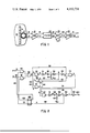
- FIG. 1 is a representational block diagram of a portion of a preferred embodiment of the present invention
- FIG. 2 is a circuit schematic of a portion of a preferred embodiment of the present invention.
- FIG. 3 illustrates various waveforms at different portions of the circuit schematic of FIG. 2.
- FIG. 1 illustrates in block diagram form the wave-shaping portion of the read circuit.
- the wave-shaping circuitry comprises a magnetic transducing head 12 for reading recorded information from a track 11 of a magnetic medium 10 moving relative to transducing head 12, in a manner well known to those skilled in the art.
- the alternating current playback signal generated by read head 12 is conducted over lines 13 and 14 to amplifier 15, which amplifies the playback signal.
- the amplified playback signal is subsequently transmitted over lines 16 and 17 to filter 20, the function of which is to remove noise components from the amplified playback signal.
- the filtered playback signal is then input over lines 21 and 22 into differentiator 25. Differentiator 25 differentiates the filtered signal, producing a zero-valued signal at each peak, whether true or false, in the playback signal.
- the differentiated playback signal is then transmitted over lines 26 and 27 to comparator 30.
- Comparator 30 generates an intermediate playback signal P over line 31 and its complement P over line 32.
- Intermediate playback signal P has a first level when the differentiated playback signal input into comparator 30 has a positive value and has a second value when the differentiated playback signal has a negative value, with transitions occurring when the differentiated playback signal value is zero.
- the transitions between levels in the intermediate playback signal P represent the occurrence of peaks, true or false, in the detected playback signal. In the case of false peaks, two relatively fast transitions occur in the intermediate playback signal P. Without proper signal processing, these transitions may be interpreted incorrectly as true signal peaks.
- the logic circuitry shown in FIG. 2 and described hereinafter eliminates the false peaks from the output signal which is ultimately generated by the read circuit of the present invention.
- FIG. 2 shows a circuit schematic of a portion of a preferred embodiment of the present invention.
- a comparator comprising AND gates 40 and 41 and NOR gate 42 receives as one set of inputs the intermediate playback signal P and its complement P and as a second set of signals the Q and Q outputs of a delay flip-flop 120.
- the P and Q signals are input to AND gate 40 over lines 31 and 131, respectively, while the P and Q signals are input into AND gate 41 over lines 32 and 132, respectively.
- the outputs of AND gates 40 and 41 are input into NOR gate 42.
- the output of NOR gate 42 is transmitted into a first delay means comprising NAND gate 50, inverter 51, capacitor 52, resistor 53, inverter 54, and inverter 55.
- the first delay means functions as a monostable multivibrator or "one-shot", which generates a signal having a predetermined level for a predetermined time interval after receiving a triggering impulse. The duration of the time interval is determined by the particular values of capacitor 52, resistor 53, and the source of direct current voltage V CC . From FIG. 2 it can be seen that the output of NAND gate 50 is input into inverter 51, whose output is connected to one side of capacitor 52.
- capacitor 52 is connected to voltage source V CC by way of resistor 53 as well as to inverter 54, whose output is input into inverter 55.
- the output of inverter 55 is fed back over line 56 as an input to NAND gate 50.
- the output of inverter 55 is also transmitted as an input to NAND gate 70.
- NAND gate 70 also receives as an input a signal J transmitted over line 62 from a disabling circuit comprising NOR gates 60 and 61, whose function will explained hereinafter.
- NOR gate 60 receives as one input the output from inverter 54 over line 64 and as a second input the output of NOR gate 61 over lines 62 and 63.
- the output of NOR gate 60 is transmitted over line 44 as one input into NOR gate 61.
- the output to NOR gate 42 is transmitted over line 43 as the other input to NOR gate 61.
- the output of NOR gate 61 is transmitted via line 62 to one input of NAND gate 70.
- the output of NAND gate 70 is transmitted over line 75 as one input to NAND gate 80, which forms part of a second delay means.
- the second delay means comprises NAND gate 80, inverter 81, capacitor 82, resistor 83, inverter 84, and inverter 85.
- the output of NAND gate 80 is the input to inverter 81, whose output is connected to one side of capacitor 82.
- the other side of capacitor 82 is connected to direct current voltage V CC through resistor 83 and to the input of inverter 84.
- the output of inverter 84 forms the input of inverter 85, whose output is fed back over line 86 as the second input to NAND gate 80.
- inverter 85 The output of inverter 85 is the input to inverter 90, whose output is connected to terminal 100, at which terminal the output signal of the read circuit is transmitted.
- the output of inverter 84 is also transmitted over line 88 to the clock input C of delay flip-flop 120.
- the complement of the intermediate playback signal P is transmitted over lines 32 and 33 to the D input of delay flip-flop 120.
- AND gates 40 and 41 provide a logical AND function to signals applied to their input leads.
- a binary 1 is represented by a positive signal, and a binary 0 by a zero-valued signal.
- An AND gate provides a positive-valued output signal if and only if both its inputs are positive-valued, representing binary 1's.
- an AND gate provides a zero-valued output signal, representing a binary 0, when either or both of its inputs are zero-valued, representing binary 0's.
- NAND gates 50, 70, and 80 provide a logical NAND function to signals applied to their input leads.
- a NAND gate provides a zero-valued output signal if and only if both of its input leads are positive-valued, representing binary 1's.
- a NAND gate generates a positive-valued output signal, representing a binary 1, when either or both of its inputs are zero-valued, representing binary 0's.
- NOR gates 42, 60 and 61 provide a logical NOR function to signals applied to them.
- a NOR gate generates a positive-valued output, representing a binary 1, if and only if both its inputs are zero-valued, representing binary 0's.
- NOR gate generates a zero-valued output signal, representing a binary zero, when either or both of its inputs are positive-valued, representing binary 1's.
- Inverters 51, 54, 55, 81, 84, 85, and 90 each provide the logical inversion of a signal applied thereto.
- An inverter provides a positive output signal representing a binary 1 when the input signal applied thereto is zero-valued representing a binary 0.
- an inverter provides an output signal representing a binary 0 when the input signal represents a binary 1.
- Delay flip-flop 120 is a logic circuit operating in either one of two stable states.
- Delay flip-flop 120 has a D (delay) input and a C (clock) input and Q and Q outputs. Each triggering impulse received at the C input causes the Q output to assume the binary level which was present at the D input immediately preceding the trigger pulse. The Q output is the complement of the Q output.
- the individual logic circuit components namely the AND's, NAND's, NOR's, inverters, and delay flip-flop, are all well known to one of ordinary skill in the art and are commercially available.
- signal H is also a binary 1.
- signal A input to NAND gate 50 is 0, and signal H input is 1, causing the resultant output B to be 1.
- the binary 1 input to inverter 51 causes its output E to go to 0, thereby discharging capacitor 52 and causing signal F also to go to 0.
- Signal G correspondingly rises to a binary 1, and signal H falls to a binary 0.
- signal F goes high, representing a binary 1
- signal H represents a binary 1 input to NAND gate 70.
- signal K generated by NAND gate 70 goes to 0 for a brief time.
- NAND gate 80 generates a 1
- inverter 81 generates a 0, and capacitor 82 discharges. Consequently, signal ⁇ goes high for the period of time required to recharge capacitor 82.
- signal R at output terminal 100 goes high for the time during which capacitor 82 is recharged to its high state.
- the time delay of the second delay means is set so as to create a pulse of approximately 200 nanoseconds in width.
- intermediate playback signal P switches from a 1 to a 0, where it remains for a sufficient period of time (at least until time t 5 ) for it to be categorized as representing the detection of a true peak.
- time t 4 , t 5 , and t 6 the operation of the logic circuitry of FIG. 2 is substantially identical to that described above regarding its operation at times t 1 , t 2 , and t 3 .
- the read circuit of the present invention does not itself reintroduce peak shift into the playback signal, in contrast to prior art read circuits.
- the series architecture of the present invention treats both negative and positive peaks in the playback signal in identical fashion, so that the rise and fall times and signal delays introduced by the logic circuit components affect both positive and negative peaks equally. Thus, no asymmetry is introduced into the output signal as between positive and negative peaks.
- signals P and P change state relative to signals Q and Q, such as at times t 1 , t 4 , and t 7 for example, the signals at each point in the logic circuit change in identical fashion.
- signals A, B, E- ⁇ , and R react identically.
- signals A, B, and E-J react identically to the same signals upon detection of a true positive or negative peak.
Landscapes
- Engineering & Computer Science (AREA)
- Signal Processing (AREA)
- Digital Magnetic Recording (AREA)
- Signal Processing For Digital Recording And Reproducing (AREA)
Priority Applications (8)
| Application Number | Priority Date | Filing Date | Title |
|---|---|---|---|
| US05/862,467 US4152731A (en) | 1977-12-20 | 1977-12-20 | Read circuit for distinguishing false peaks in an alternating current playback signal |
| GB7844396A GB2010555B (en) | 1977-12-20 | 1978-11-14 | Read circuit |
| DE2850468A DE2850468C2 (de) | 1977-12-20 | 1978-11-21 | Leseschaltung |
| JP14524378A JPS5487513A (en) | 1977-12-20 | 1978-11-24 | Reader circuit |
| FR7834697A FR2412901A1 (fr) | 1977-12-20 | 1978-12-08 | Circuit de lecture |
| SG182/84A SG18284G (en) | 1977-12-20 | 1984-02-29 | Read circuit for eliminating false peaks in an alternating current playback signal |
| HK665/84A HK66584A (en) | 1977-12-20 | 1984-08-23 | Read circuit for eliminating false peaks in an alternating current playback signal |
| MY492/85A MY8500492A (en) | 1977-12-20 | 1985-12-30 | Read circuit for eliminating false peaks in an alternating current playback signal |
Applications Claiming Priority (1)
| Application Number | Priority Date | Filing Date | Title |
|---|---|---|---|
| US05/862,467 US4152731A (en) | 1977-12-20 | 1977-12-20 | Read circuit for distinguishing false peaks in an alternating current playback signal |
Publications (1)
| Publication Number | Publication Date |
|---|---|
| US4152731A true US4152731A (en) | 1979-05-01 |
Family
ID=25338565
Family Applications (1)
| Application Number | Title | Priority Date | Filing Date |
|---|---|---|---|
| US05/862,467 Expired - Lifetime US4152731A (en) | 1977-12-20 | 1977-12-20 | Read circuit for distinguishing false peaks in an alternating current playback signal |
Country Status (8)
| Country | Link |
|---|---|
| US (1) | US4152731A (de) |
| JP (1) | JPS5487513A (de) |
| DE (1) | DE2850468C2 (de) |
| FR (1) | FR2412901A1 (de) |
| GB (1) | GB2010555B (de) |
| HK (1) | HK66584A (de) |
| MY (1) | MY8500492A (de) |
| SG (1) | SG18284G (de) |
Cited By (1)
| Publication number | Priority date | Publication date | Assignee | Title |
|---|---|---|---|---|
| US5305156A (en) * | 1991-10-18 | 1994-04-19 | Teac Corporation | Digital data storage apparatus comprising circuit for reducing read errors |
Citations (3)
| Publication number | Priority date | Publication date | Assignee | Title |
|---|---|---|---|---|
| US3404391A (en) * | 1964-07-08 | 1968-10-01 | Data Products Corp | Binary digit discriminator |
| US3597751A (en) * | 1969-04-21 | 1971-08-03 | Ibm | Signal recovery system for use with magnetic media |
| US3623040A (en) * | 1969-06-25 | 1971-11-23 | Scient Data Systems Inc | Digital decoding of reproduced signals |
Family Cites Families (4)
| Publication number | Priority date | Publication date | Assignee | Title |
|---|---|---|---|---|
| US3243580A (en) * | 1960-12-06 | 1966-03-29 | Sperry Rand Corp | Phase modulation reading system |
| NL7003326A (de) * | 1969-03-18 | 1970-09-22 | ||
| JPS5143367B2 (de) * | 1972-07-07 | 1976-11-20 | ||
| US4012785A (en) * | 1976-02-13 | 1977-03-15 | Shugart Associates, Inc. | Magnetic recording playback circuit |
-
1977
- 1977-12-20 US US05/862,467 patent/US4152731A/en not_active Expired - Lifetime
-
1978
- 1978-11-14 GB GB7844396A patent/GB2010555B/en not_active Expired
- 1978-11-21 DE DE2850468A patent/DE2850468C2/de not_active Expired
- 1978-11-24 JP JP14524378A patent/JPS5487513A/ja active Pending
- 1978-12-08 FR FR7834697A patent/FR2412901A1/fr active Pending
-
1984
- 1984-02-29 SG SG182/84A patent/SG18284G/en unknown
- 1984-08-23 HK HK665/84A patent/HK66584A/xx unknown
-
1985
- 1985-12-30 MY MY492/85A patent/MY8500492A/xx unknown
Patent Citations (3)
| Publication number | Priority date | Publication date | Assignee | Title |
|---|---|---|---|---|
| US3404391A (en) * | 1964-07-08 | 1968-10-01 | Data Products Corp | Binary digit discriminator |
| US3597751A (en) * | 1969-04-21 | 1971-08-03 | Ibm | Signal recovery system for use with magnetic media |
| US3623040A (en) * | 1969-06-25 | 1971-11-23 | Scient Data Systems Inc | Digital decoding of reproduced signals |
Cited By (1)
| Publication number | Priority date | Publication date | Assignee | Title |
|---|---|---|---|---|
| US5305156A (en) * | 1991-10-18 | 1994-04-19 | Teac Corporation | Digital data storage apparatus comprising circuit for reducing read errors |
Also Published As
| Publication number | Publication date |
|---|---|
| DE2850468A1 (de) | 1979-09-13 |
| GB2010555A (en) | 1979-06-27 |
| FR2412901A1 (fr) | 1979-07-20 |
| DE2850468C2 (de) | 1986-02-20 |
| SG18284G (en) | 1985-03-08 |
| HK66584A (en) | 1984-08-31 |
| GB2010555B (en) | 1982-03-31 |
| JPS5487513A (en) | 1979-07-12 |
| MY8500492A (en) | 1985-12-31 |
Similar Documents
| Publication | Publication Date | Title |
|---|---|---|
| US3271750A (en) | Binary data detecting system | |
| US3585507A (en) | Pulse discrimination circuitry | |
| US3905029A (en) | Method and apparatus for encoding and decoding digital data | |
| US4417213A (en) | Data regenerative system for NRZ mode signals | |
| US5105316A (en) | Qualification for pulse detecting in a magnetic media data storage system | |
| EP0181784B1 (de) | Erzeugungssystem für Digitalsignale und Verfahren dafür | |
| US4152731A (en) | Read circuit for distinguishing false peaks in an alternating current playback signal | |
| US3821716A (en) | Method and apparatus for recovering data in an nrzi recording system | |
| US3506923A (en) | Binary data detection system | |
| US5920440A (en) | Gray code decoding circuit of a hard disk drive | |
| JPS59113516A (ja) | マルチチヤネル読取り信号再生システム | |
| US3559178A (en) | Pulse discrimination circuitry | |
| US5420726A (en) | Channel qualifier for a hard disk drive which differentiates a raw data signal before peak detection and qualification of the signal | |
| US3852810A (en) | Self-clocking nrz recording and reproduction system | |
| US4876615A (en) | Data decoding system | |
| US3665327A (en) | Noise discriminator for digital data detection system | |
| US3774178A (en) | Conversion of nrz data to self-clocking data | |
| ES334929A1 (es) | Una disposicion para deteccion de senales binarias. | |
| JPS6361812B2 (de) | ||
| US3733579A (en) | Sensing device for digital magnetic memory | |
| US3626395A (en) | Dual clocking recording and reproducing system for magnetic data | |
| JPS595965B2 (ja) | デイジタル記録におけるクロツク信号抽出回路 | |
| JPS5943860B2 (ja) | フレ−ム同期信号検出回路 | |
| US5570380A (en) | Survival sequence register for variable threshold qualification for recording channels | |
| JP3148358B2 (ja) | 信号のデューティ比識別回路 |