US3661580A - Photographic method for producing a cathode-ray tube screen structure - Google Patents
Photographic method for producing a cathode-ray tube screen structure Download PDFInfo
- Publication number
- US3661580A US3661580A US7138A US3661580DA US3661580A US 3661580 A US3661580 A US 3661580A US 7138 A US7138 A US 7138A US 3661580D A US3661580D A US 3661580DA US 3661580 A US3661580 A US 3661580A
- Authority
- US
- United States
- Prior art keywords
- light
- film
- stencil
- layer
- exposed
- Prior art date
- Legal status (The legal status is an assumption and is not a legal conclusion. Google has not performed a legal analysis and makes no representation as to the accuracy of the status listed.)
- Expired - Lifetime
Links
Images

Classifications
-
- H—ELECTRICITY
- H01—ELECTRIC ELEMENTS
- H01J—ELECTRIC DISCHARGE TUBES OR DISCHARGE LAMPS
- H01J9/00—Apparatus or processes specially adapted for the manufacture, installation, removal, maintenance of electric discharge tubes, discharge lamps, or parts thereof; Recovery of material from discharge tubes or lamps
- H01J9/20—Manufacture of screens on or from which an image or pattern is formed, picked up, converted or stored; Applying coatings to the vessel
- H01J9/22—Applying luminescent coatings
- H01J9/227—Applying luminescent coatings with luminescent material discontinuously arranged, e.g. in dots or lines
- H01J9/2271—Applying luminescent coatings with luminescent material discontinuously arranged, e.g. in dots or lines by photographic processes
Definitions
- the tube includes an aperture mask (also called a shadow mask) having an array of apertures therein closely spaced from the inner surface of the glass viewing panel of the tube.
- a light-absorbing layer or matrix having an array of holes or openings therein filled with luminescent material resides on the inner surface of the viewing panel.
- each aperture in the mask has three related smaller sized holes in the matrix, each hole being filled with a different color emission luminescent material.
- the novel process produces a screen structure for a cathode-ray tube including a light-absorbing layer or matrix having an array of holes therein.
- a stencil having an array of opaque areas is produced on a supporting surface, such as the inner surface of the viewing panel of a cathode-ray tube.
- the opaque areas of the stencil have the correct center to center spacing but are larger in size than the desired holes in the matrix.
- the stencil is preferably made photographically by back exposure using a process which includes projecting light through the apertures of an aperture mask which has been positioned in the viewing panel, incident upon a photopolymeric layer on the inner surface of the viewing panel.
- a photopolymeric film is deposited over the stencil and supporting surface and exposed by front flood exposure; that is, light is passed through the supporting surface and stencil to expose the film. At least a portion of the light in the film is scattered during this exposing step so that the exposed areas of the film extend behind the opaque areas of the stencil leaving the unexposed areas of the film substantially the same sizes as the desired matrix holes.
- This scattering may be achieved, for example, by including light-scattering particles in the film, or by overcoating the film with a light-scattering layer, or by placing a reflective light-scattering surface adjacent to the film.
- the unexposed areas of the film are removed, while the exposed areas are retained in place.
- the retained film areas are rendered lightabsorbing; the stencil is removed; and the holes left in the film are filled with luminescent material.
- the exposure and development of the photopolymeric film are less critical than in previous processes. Also, by the novel process, a greater controlled reduction from mask aperture size to matrix hole size may be achieved than by previous processes. This permits larger mask apertures relative to the matrix holes to be used. As a result, the dimensional tolerance of electron beam landing in the finished tube is relaxed.
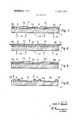
- FIGS. 1 through 6 are fragmentary sectional views through a fragment of the faceplate panel of a cathode-ray tube showing different stages of completion of a screen structure prepared by one embodiment of the novel method.
- FIGS. 7 and 8 are fragmentary sectional views through a faceplate panel showing two alternative ways for producing light scattering in other embodiments of the novel method.
- FIGS. 9 and 10 are fragmentary sectional views through a faceplate panel illustrating an alternative way of rendering the matrix light absorbing.
- FIGS. 1 through 6 illustrate some of the steps, according to one embodiment of the invention, used in preparing a screen structure comprising a light-absorbing matrix having an array of holes or openings therein filled with luminescent material for a shadow mask type color television picture tube.
- FIG. 1 shows a fragment of the viewing panel 21 for this tube having thereon a stencil comprised of an array of opaque areas 23R, 236, and 238.
- the stencil may be preparedby the following steps.
- the inner surface 25 of the viewing panel 21 is cleaned, coated with an aqueous solution containing 3 weight percent USP gelatin and 1 weight percent neutralized ammonium dichromate as a photosensitizer, and then dried.
- the shadow mask associated with the panel 21 is positioned on its studs and then placed on a first lighthouse where light from a small area source at a first position is projected through the mask incident upon the coating to expose one set of areas designated 23R for the red-emitting luminescent material.
- the panel 21 is placed on a second lighthouse where light from a small area source at a second position is projected through the maskincident upon the coating to expose a second set of areas designated 236 for the green-emitting luminescent material.
- the steps are repeated in a third lighthouse with the small area light source at a third position to produce a third set of areas designated 23B for the blue-emitting luminescent material.
- an aperture mask having apertures of about 15.5 mils diameter is placed on a lighthouse having a 1,000 watt BI-I6 mercury vapor lamp in a light box with a light pipe or collimator that terminates in a mil diameter tip, which constitutes the small area light source.
- a 10 minutes exposure of the coating with the light source positioned about 14 inches from the aperture mask on the lighthouse produces exposed areas which are about 16.5 mils in diameter.
- the aperture mask is now removed from the panel 21 and the exposed gelatin layer is saturated with an alcohol solution of nigrosine black dye, which is applied by spraying or flow coating, and then dried.
- the dyed and exposed layer is developed in a stream of cool water for about 15 minutes and then in a stream of 45 C. water for about 60 seconds and then dried.
- the water stream dissolves away the unexposed portions of the gelatin layer leaving the dyed exposed areas 23R, 23G, and 233 in place as shown in FIG. 1, which dyed areas comprise the opaque areas of the stencil.
- the opaque areas of the stencil and the bare surface'areas 25 of the panel 21 are coated with an aqueous solution containing 15 weight percent manganese oxalate, 5 weight percent 50-42 polyvinyl alcohol and 0.5 weight percent ammonium dichromate sensitizer for the polyvinyl alcohol.
- the slurry is spin coated on and then dried, producing a film 27 of photopolymeric material as shown in FIG. 2.
- the panel is now placed opposite a bank of ultraviolet emitting lamps with the stencil and coating on the remote side of the panel 21 from the lamp.
- An exposure of about 15 minutes to three 40-watt fluorescent lamps spaced about 8 inches from the panel has been found to be satisfactory.
- the manganese oxalate in the film 27 is pinkish white in color, and particles thereof in the film 27 scatter the light therein so that portions of the film a short distance behind the opaque areas 23R, 230 and 23B are exposed.
- the film 27 is exposed inward behind opaque areas leaving unexposed areas about 13 mils in diameter behind the opaque areas.
- the layer 27 is developed by applying a spray of deionized water with a line pressure of about 25 pounds per square inch for about 1 to 2 minutes until the unexposed areas of the film are completely dissolved and are free of manganese oxalate.
- the exposed areas of the film 27 are retained in place and overlap the opaque areas of the stencil, as shown in FIG. 4.
- the structure may be washed at this point with dilute aqueous ammonium hydroxide to convert part or all of the manganese oxalate to black manganese oxide.
- red-emitting dots 31R of luminescent materials, green-emitting dots 316 of luminescentmaterials and blueemitting dots 31B of luminescent materials are deposited photographically in the usual manner for a shadow mask tube, producing the structure shown in FIG. 5.
- the matrix is coated with green-emitting phosphor particles in a photopolymeric binder, the coating exposed in a lighthouse though the mask and the exposed coating developed to produce the green-emitting dots 31G.
- the sequence is repeated with blue-emitting phosphor and again repeated with red-emitting phosphor to produce the blue-emitting dots 31B and red-emitting dots 31R.
- the structure is filmed and a layer of aluminum metal is vapor deposited upon the structure.
- the structure is baked, generally at temperatures of about 400 to 450 C., in air to remove volatile matter.
- the stencil including any dye contained therein, is volatilized along with other organic matter and any manganese oxalate present is converted to black manganese oxide.
- the finished screen structure is shown in FIG. 6 comprising a light-absorbing matrix 27 having therein an array of holes filled with luminescent materials 31R, 316 and 31B and a layer of specular aluminum 32 over the luminescent materials.
- the panel may now be assembled into a cathode-ray tube, such as a color television picture tube, by known processing techniques.
- Example 2 The procedure in this example is the same as for Example 1 except that the stencil is made by the following steps with reference to FIGS. 1 and 2.
- the inner surface 25 of the panel 21 is cleaned and coated with an aqueous solution containing 3 weight percent 50-42 polyvinyl alcohol and 0.5 weight percent sodium dichromate as a photosensitizer, and then dried.
- the shadow mask associated with the panel 21 is positioned on its studs and then back exposed three times as described in Example I.
- the aperture mask is now removed from the panel 21 and the exposed polyvinyl alcohol layer developed in a stream of warm water for about 15 minutes. The water stream washes away the unexposed portions of the layer leaving the exposed portions in place. Now the retained exposed portions of the layer are dyed to render them opaque.
- an aqueous solution containing about 5 percent nigrosine black dye, is applied, as by slurrying, to the layer and permitted to dry.
- An aqueous 1.0 weight percent solution of a heavy metal salt, such as barium acetate, is sloshed over the dye to set or insolubilize the dye on the exposed portions of the layer.
- Example 1 The steps for producing the matrix and luminescent areas are the same as for Example 1.
- the stencil may be prepared by any convenient process.
- the stencil is prepared by exposing and developing a photopolymeric layer .to produce a polymeric image which is then rendered opaque by saturation with a dye.
- polymeric image nontransmitting may be used, for example particles of carbon, or metal, or a material such as silver chloride which can later be converted to an opaque material.
- Another alternative to making the stencil is first to deposit an opaque layer such as silver metal on the surface and a photoresist layer thereover. The photoresist layer is exposed to a light image and developed, and then the areas of the opaque layer not covered by the resist are dissolved away as with acid or other suitable reagent, leaving a stencil of opaque areas.
- Still another method of making a stencil is to use a silver halide emulsion layer which is exposed and developed in the usual way to produce opaque areas.
- the stencil is coated with a film 27 of photopolymeric material. containing a light-scattering material. Then, the film is front flooded through the faceplate panel to produce a hardening or insolubilizing of the film. Due to the scattering of light in the film, additional hardening takes place inward from the edge of and behind the opaque areas of the stencil. After the correct exposure to give the final desired hole size, development of the light-scattering film leaves a hole behind each opaque area of the stencil.
- the light-scattering material is a material which upon baking converts to a permanent light-absorbing layer, such as a manganese oxalate or manganese tartrate being converted to manganese oxide
- the development step is sufficient but otherwise, the printed pattern of the film must be blackened with a permanent opaquing material in order to produce the light-absorbing matrix.
- any of a large number of organic or inorganic light-scattering materials which do not blacken may be used in the photopolymeric film.
- Some examples are titanium dioxide, acrylic beads and aluminum oxide.
- an organic or inorganic light-scattering material may be used and the flood-exposed film subsequently blackened with a permanent blackening material such as graphite.
- a permanent blackening material such as graphite.
- the permanent blackening material such as channel black or graphite to be incorporated directly in the photopolymeric film.
- FIG. 7 illustrates an alternative method for achieving lightscattering.
- the stencil is coated with a clear photopolymeric film 27a, which is overcoated with a light-scattering layer 33 comprised, for example, of silica particles with or without a binder.
- a light-scattering layer 33 comprised, for example, of silica particles with or without a binder.
- Light flooding through the panel 21 and the stencil 23 passes through the film 27a and is scattered back off the overcoating 33 thereby exposing the film behind the opaque areas 23R, 23G and 238.
- a reflective surface such as a paper sheet 35 is placed behind a clear photopolymeric film 27a to scatter light which has passed through the stencil and film.
- the alternatives shown in FIGS. 7 and 8 have the advantage of having a clear spacer layer which permits somewhat greater penetration of scattered light behind the opaque areas of the stencil.
- any negative acting photopolymeric may be used in the films 27 and 27a.
- Polyvinyl alcohol sensitized with a dichromate is preferred. Sensitized gelatin, glue, shellac, KPR or KOR may also be used.
- the exposure is tailored to the particular photopolymeric material used and to the particular application. Developing the exposed film is also tailored to the particular photopolymeric material and to the particular application. When a dye or other volatile organic material such as carbon is used as a stencil material, clearing of the hole may take place during baking out of the panel.
- Developing of the film can be accomplished with a solubilizing reagent for the blackening pigment; for example, an acid which dissolves metals or their salts, where thestencil is constituted of all metal salts.
- developing of the film can also be achieved by applying a reagent which attacks the polymer. For example, when forming the matrix, then an enzyme, such as gelatinase, can be used to develop the matrix.
- the light-scattering material is such that when heated, it renders the retained film areas opaque, thereby producing the desired light-absorbing quality to the matrix.
- This may be achieved with a number of metal salts.
- Such a material may also be incorporated in the scattering layer 33 in FIG. 7.
- the material for rendering the retained film regions blackened or otherwise rendered opaque is introduced after exposure, as would be necessary for the structure shown in FIG. 8. This may be achieved by overcoating the exposed film 27A with a layer 35 of an opaque material such as graphite, manganese dioxide or iron oxide in a blinder as shown in FIG. 9. In the development of the film 27A, the opaque material overlying the retained film regions is retained, while the rest of the overcoating is carried away during development yielding the structure shown in FIG. 10.
- the structure is rinsed withwater, dried for about 4 minutes with the aid of infrared heat and the desired luminescent material deposited thereon by any of the known photographic techniques using the same aperture mask that had been used for making the matrix.
- the phosphor dots are somewhat larger than the holes in the light-absorbing matrix and also larger than the apertures in the aperture mask.
- FIG. 6 shows the light-absorbing matrix with the smaller holes therein and the larger phosphor dots being substantially concentric therewith.
- a suitable process for depositing the phosphor dots 23R, 236 and 23B is described in an article entitled, Color-Television Screening by the Slurry Process," By T. A. Saulnier, Jr. in Electrochemical Technology, 4,27-31 (1966).
- the luminescent screen may now be processed in the usual way to apply a reflective metal layer on top of the phosphor dots and the light-absorbing matrix.
- the screen structure is then baked at temperatures between'about 400 and 450 C. and then assembled with the aperture mask into a cathode-ray tube in any of the known procedures.
- a suitable process for filming and metalizing the screen structure is described in an article entitled, Emulsion Filming with Color Television Screens," T. A. Saulnier, Jr. in Electrochemical Technology, 4, 31-34, (1966).
- a method for producing a screen structure for a cathode-ray tube comprising a light-absorbing layer having therein an array of light-transmitting holes filled with luminescent material, the steps including:
- a method for producing a screen structure for a cathoderay tube having a screen structure including (a) a light-absorbing layer having therein an array of light-transmitting holes filled with luminescent material and (b) a shadow mask spaced from said layer, said mask having therein an array of apertures that are larger in size than said holes, the steps comprising:
- step (2) is comprised of (a) a water-soluble organic polymeric material which volatilizes upon heating and (b) a light-scattering, inorganic salt which, upon heating, decomposes to a darkcolored light-absorbing compound; and step (6) includes heating said retained exposed areas of the film to volatilize said polymeric material and to convert said inorganic salt to a dark-colored, light-absorbing compound.
Landscapes
- Engineering & Computer Science (AREA)
- Manufacturing & Machinery (AREA)
- Formation Of Various Coating Films On Cathode Ray Tubes And Lamps (AREA)
- Cathode-Ray Tubes And Fluorescent Screens For Display (AREA)
Applications Claiming Priority (1)
| Application Number | Priority Date | Filing Date | Title |
|---|---|---|---|
| US713870A | 1970-01-30 | 1970-01-30 |
Publications (1)
| Publication Number | Publication Date |
|---|---|
| US3661580A true US3661580A (en) | 1972-05-09 |
Family
ID=21724442
Family Applications (1)
| Application Number | Title | Priority Date | Filing Date |
|---|---|---|---|
| US7138A Expired - Lifetime US3661580A (en) | 1970-01-30 | 1970-01-30 | Photographic method for producing a cathode-ray tube screen structure |
Country Status (5)
| Country | Link |
|---|---|
| US (1) | US3661580A (OSRAM) |
| JP (1) | JPS49747B1 (OSRAM) |
| DE (1) | DE2103308A1 (OSRAM) |
| FR (1) | FR2077017A5 (OSRAM) |
| GB (1) | GB1311372A (OSRAM) |
Cited By (19)
| Publication number | Priority date | Publication date | Assignee | Title |
|---|---|---|---|---|
| US3858083A (en) * | 1973-05-07 | 1974-12-31 | Gte Sylvania Inc | Cathode ray tube screen structure |
| US3878427A (en) * | 1973-02-05 | 1975-04-15 | Rca Corp | Apertured-mask cathode-ray tube having half-tone array of heat-absorbing areas on target surface |
| US3953621A (en) * | 1974-03-21 | 1976-04-27 | Gte Sylvania Incorporated | Process of forming cathode ray tube screens |
| US3966474A (en) * | 1974-11-25 | 1976-06-29 | Rca Corporation | Method for improving adherence of phosphor-photobinder layer during luminescent-screen making |
| US3981729A (en) * | 1973-05-14 | 1976-09-21 | Rca Corporation | Photographic method employing organic light-scattering particles for producing a viewing-screen structure |
| US3992207A (en) * | 1974-03-11 | 1976-11-16 | U.S. Philips Corporation | Method of manufacturing a cathode-ray tube for the display of colored images |
| US4019905A (en) * | 1974-06-17 | 1977-04-26 | Hitachi, Ltd. | Method for forming fluorescent screen of color cathode ray tubes using filter layer |
| US4045224A (en) * | 1972-12-25 | 1977-08-30 | Hitachi, Ltd. | Method for making phosphor screen for black matrix type color picture tube using two light sources |
| US4141731A (en) * | 1973-10-01 | 1979-02-27 | Mca Disco-Vision, Inc. | Method of creating a replicating matrix |
| US4174219A (en) * | 1976-12-23 | 1979-11-13 | International Business Machines Corporation | Method of making a negative exposure mask |
| US4223083A (en) * | 1977-12-27 | 1980-09-16 | Tektronix, Inc. | Virtual mask exposure system for CRT screen manufacture |
| US4252889A (en) * | 1976-09-24 | 1981-02-24 | Thomson-Brandt | Process of making an optically recordable and readable information carrier and the carrier obtained by this process |
| US4369241A (en) * | 1980-03-19 | 1983-01-18 | Hitachi, Ltd. | Method of forming a fluorescent screen of a black matrix type color picture tube |
| US4419425A (en) * | 1981-05-20 | 1983-12-06 | Matsushita Electric Industrial Co., Ltd. | Method for manufacturing color filter |
| US4572880A (en) * | 1978-10-25 | 1986-02-25 | Hitachi, Ltd. | Method of manufacturing fluorescent screens |
| US4670364A (en) * | 1982-05-18 | 1987-06-02 | Comtech Research Unit Limited | Photomask for electrophotography |
| US4990417A (en) * | 1987-02-23 | 1991-02-05 | Sony Corporation | Method of manufacturing a cathode ray tube |
| US5148082A (en) * | 1989-07-11 | 1992-09-15 | Kabushiki Kaisha Toshiba | Color picture tube with light absorbing layer on screen |
| WO1998043747A1 (en) * | 1997-03-31 | 1998-10-08 | Candescent Technologies Corporation | Black matrix with conductive coating |
Families Citing this family (2)
| Publication number | Priority date | Publication date | Assignee | Title |
|---|---|---|---|---|
| JPS5396344U (OSRAM) * | 1977-01-07 | 1978-08-05 | ||
| JPS53141736U (OSRAM) * | 1977-04-13 | 1978-11-09 |
Citations (6)
| Publication number | Priority date | Publication date | Assignee | Title |
|---|---|---|---|---|
| US3146368A (en) * | 1961-04-04 | 1964-08-25 | Rauland Corp | Cathode-ray tube with color dots spaced by light absorbing areas |
| US3226246A (en) * | 1960-08-06 | 1965-12-28 | Philips Corp | Method of manufacturing display screens for cathode-ray tubes |
| US3287130A (en) * | 1964-08-25 | 1966-11-22 | Rauland Corp | Process of cathode-ray tube screening comprising a backward exposure step |
| US3365292A (en) * | 1968-01-23 | Rauland Corp | Method of establishing a light absorbing design on a screen structure of an image reproducer | |
| US3514287A (en) * | 1961-10-09 | 1970-05-26 | Rca Corp | Photographic method for making tri-colored cathode ray screen |
| US3533791A (en) * | 1967-01-06 | 1970-10-13 | Philco Ford Corp | Process for fabricating multicolor image screens |
-
1970
- 1970-01-30 US US7138A patent/US3661580A/en not_active Expired - Lifetime
- 1970-12-17 JP JP45114958A patent/JPS49747B1/ja active Pending
-
1971
- 1971-01-15 GB GB207571*[A patent/GB1311372A/en not_active Expired
- 1971-01-25 DE DE19712103308 patent/DE2103308A1/de active Pending
- 1971-01-27 FR FR7102607A patent/FR2077017A5/fr not_active Expired
Patent Citations (6)
| Publication number | Priority date | Publication date | Assignee | Title |
|---|---|---|---|---|
| US3365292A (en) * | 1968-01-23 | Rauland Corp | Method of establishing a light absorbing design on a screen structure of an image reproducer | |
| US3226246A (en) * | 1960-08-06 | 1965-12-28 | Philips Corp | Method of manufacturing display screens for cathode-ray tubes |
| US3146368A (en) * | 1961-04-04 | 1964-08-25 | Rauland Corp | Cathode-ray tube with color dots spaced by light absorbing areas |
| US3514287A (en) * | 1961-10-09 | 1970-05-26 | Rca Corp | Photographic method for making tri-colored cathode ray screen |
| US3287130A (en) * | 1964-08-25 | 1966-11-22 | Rauland Corp | Process of cathode-ray tube screening comprising a backward exposure step |
| US3533791A (en) * | 1967-01-06 | 1970-10-13 | Philco Ford Corp | Process for fabricating multicolor image screens |
Cited By (26)
| Publication number | Priority date | Publication date | Assignee | Title |
|---|---|---|---|---|
| US4045224A (en) * | 1972-12-25 | 1977-08-30 | Hitachi, Ltd. | Method for making phosphor screen for black matrix type color picture tube using two light sources |
| US3878427A (en) * | 1973-02-05 | 1975-04-15 | Rca Corp | Apertured-mask cathode-ray tube having half-tone array of heat-absorbing areas on target surface |
| US3858083A (en) * | 1973-05-07 | 1974-12-31 | Gte Sylvania Inc | Cathode ray tube screen structure |
| US3981729A (en) * | 1973-05-14 | 1976-09-21 | Rca Corporation | Photographic method employing organic light-scattering particles for producing a viewing-screen structure |
| FR2406233A1 (fr) * | 1973-10-01 | 1979-05-11 | Mca Disco Vision | Matrice de disques et son procede de realisation |
| FR2406234A1 (fr) * | 1973-10-01 | 1979-05-11 | Mca Disco Vision | Matrice de disques et son procede de realisation |
| US4141731A (en) * | 1973-10-01 | 1979-02-27 | Mca Disco-Vision, Inc. | Method of creating a replicating matrix |
| FR2406235A1 (fr) * | 1973-10-01 | 1979-05-11 | Mca Disco Vision | Matrice de disques et son procede de realisation |
| US3992207A (en) * | 1974-03-11 | 1976-11-16 | U.S. Philips Corporation | Method of manufacturing a cathode-ray tube for the display of colored images |
| US3953621A (en) * | 1974-03-21 | 1976-04-27 | Gte Sylvania Incorporated | Process of forming cathode ray tube screens |
| US4019905A (en) * | 1974-06-17 | 1977-04-26 | Hitachi, Ltd. | Method for forming fluorescent screen of color cathode ray tubes using filter layer |
| US3966474A (en) * | 1974-11-25 | 1976-06-29 | Rca Corporation | Method for improving adherence of phosphor-photobinder layer during luminescent-screen making |
| US4288510A (en) * | 1976-09-24 | 1981-09-08 | Thomson-Brandt | Process of making an optically recordable and readable information carrier and the carrier obtained by this process |
| US4334007A (en) * | 1976-09-24 | 1982-06-08 | Thomson-Brandt | Process of making an optically recordable and readable information carrier and the carrier obtained by this process |
| US4252889A (en) * | 1976-09-24 | 1981-02-24 | Thomson-Brandt | Process of making an optically recordable and readable information carrier and the carrier obtained by this process |
| US4174219A (en) * | 1976-12-23 | 1979-11-13 | International Business Machines Corporation | Method of making a negative exposure mask |
| US4223083A (en) * | 1977-12-27 | 1980-09-16 | Tektronix, Inc. | Virtual mask exposure system for CRT screen manufacture |
| US4572880A (en) * | 1978-10-25 | 1986-02-25 | Hitachi, Ltd. | Method of manufacturing fluorescent screens |
| US4369241A (en) * | 1980-03-19 | 1983-01-18 | Hitachi, Ltd. | Method of forming a fluorescent screen of a black matrix type color picture tube |
| US4419425A (en) * | 1981-05-20 | 1983-12-06 | Matsushita Electric Industrial Co., Ltd. | Method for manufacturing color filter |
| US4670364A (en) * | 1982-05-18 | 1987-06-02 | Comtech Research Unit Limited | Photomask for electrophotography |
| US4990417A (en) * | 1987-02-23 | 1991-02-05 | Sony Corporation | Method of manufacturing a cathode ray tube |
| US5148082A (en) * | 1989-07-11 | 1992-09-15 | Kabushiki Kaisha Toshiba | Color picture tube with light absorbing layer on screen |
| WO1998043747A1 (en) * | 1997-03-31 | 1998-10-08 | Candescent Technologies Corporation | Black matrix with conductive coating |
| US5912056A (en) * | 1997-03-31 | 1999-06-15 | Candescent Technologies Corporation | Black matrix with conductive coating |
| US6100636A (en) * | 1997-03-31 | 2000-08-08 | Candescent Technologies Corporation | Black matrix with conductive coating |
Also Published As
| Publication number | Publication date |
|---|---|
| FR2077017A5 (OSRAM) | 1971-10-15 |
| DE2103308A1 (de) | 1971-08-05 |
| JPS49747B1 (OSRAM) | 1974-01-09 |
| GB1311372A (en) | 1973-03-28 |
Similar Documents
| Publication | Publication Date | Title |
|---|---|---|
| US3661580A (en) | Photographic method for producing a cathode-ray tube screen structure | |
| US3558310A (en) | Method for producing a graphic image | |
| US3788846A (en) | Method for printing negative tolerance matrix screen structure for a cathode-ray tube | |
| US4019905A (en) | Method for forming fluorescent screen of color cathode ray tubes using filter layer | |
| US3365292A (en) | Method of establishing a light absorbing design on a screen structure of an image reproducer | |
| US3615462A (en) | Processing black-surround screens | |
| US3559546A (en) | Cathode ray tube screen exposure | |
| US3226246A (en) | Method of manufacturing display screens for cathode-ray tubes | |
| US3317319A (en) | Method of depositing particulate layers | |
| US3592112A (en) | Photographic printing of cathode-ray tube screen structure | |
| US3152900A (en) | Art of making electron-sensitive mosaic screens | |
| US3614504A (en) | Color picture tube screen with phosphors dots overlapping portions of a partial-digit-transmissive black-surround material | |
| US3406068A (en) | Photographic methods of making electron-sensitive mosaic screens | |
| US2992107A (en) | Method of manufacturing luminescent screens | |
| JPS6145530A (ja) | カラ−ブラウン管螢光面の製造方法 | |
| US4855200A (en) | Fluorescent screens of color picture tubes and manufacturing method therefor | |
| US4223083A (en) | Virtual mask exposure system for CRT screen manufacture | |
| US3887371A (en) | Photographic method for printing viewing-screen structure including treatment of exposed coating with ammonium compound | |
| US3224895A (en) | Method of manufacturing display screens for cathode-ray tubes | |
| US4152154A (en) | Method of optically projecting a pattern of substantially circular apertures on a photosensitive layer by rotating light source | |
| US3767395A (en) | Multiple exposure color tube screening | |
| US3775116A (en) | Method for making a phosphor screen of a cathode-ray tube | |
| US3484269A (en) | Process for the manufacture of a display screen of a cathode ray tube for reproducing color images employing phosphor strips luminescing in different colors and an indexing strip | |
| US3953621A (en) | Process of forming cathode ray tube screens | |
| US3672893A (en) | Process of manufacturing screens for shadow-mask tubes |
Legal Events
| Date | Code | Title | Description |
|---|---|---|---|
| AS | Assignment |
Owner name: RCA LICENSING CORPORATION, TWO INDEPENDENCE WAY, P Free format text: ASSIGNMENT OF ASSIGNORS INTEREST.;ASSIGNOR:RCA CORPORATION, A CORP. OF DE;REEL/FRAME:004993/0131 Effective date: 19871208 |