US20240128362A1 - Semiconductor device - Google Patents
Semiconductor device Download PDFInfo
- Publication number
- US20240128362A1 US20240128362A1 US18/542,814 US202318542814A US2024128362A1 US 20240128362 A1 US20240128362 A1 US 20240128362A1 US 202318542814 A US202318542814 A US 202318542814A US 2024128362 A1 US2024128362 A1 US 2024128362A1
- Authority
- US
- United States
- Prior art keywords
- region
- trench portion
- gate trench
- end region
- contact
- Prior art date
- Legal status (The legal status is an assumption and is not a legal conclusion. Google has not performed a legal analysis and makes no representation as to the accuracy of the status listed.)
- Pending
Links
Images


Classifications
-
- H—ELECTRICITY
- H10—SEMICONDUCTOR DEVICES; ELECTRIC SOLID-STATE DEVICES NOT OTHERWISE PROVIDED FOR
- H10D—INORGANIC ELECTRIC SEMICONDUCTOR DEVICES
- H10D62/00—Semiconductor bodies, or regions thereof, of devices having potential barriers
- H10D62/10—Shapes, relative sizes or dispositions of the regions of the semiconductor bodies; Shapes of the semiconductor bodies
- H10D62/102—Constructional design considerations for preventing surface leakage or controlling electric field concentration
- H10D62/103—Constructional design considerations for preventing surface leakage or controlling electric field concentration for increasing or controlling the breakdown voltage of reverse-biased devices
- H10D62/105—Constructional design considerations for preventing surface leakage or controlling electric field concentration for increasing or controlling the breakdown voltage of reverse-biased devices by having particular doping profiles, shapes or arrangements of PN junctions; by having supplementary regions, e.g. junction termination extension [JTE]
- H10D62/106—Constructional design considerations for preventing surface leakage or controlling electric field concentration for increasing or controlling the breakdown voltage of reverse-biased devices by having particular doping profiles, shapes or arrangements of PN junctions; by having supplementary regions, e.g. junction termination extension [JTE] having supplementary regions doped oppositely to or in rectifying contact with regions of the semiconductor bodies, e.g. guard rings with PN or Schottky junctions
- H10D62/107—Buried supplementary regions, e.g. buried guard rings
-
- H01L29/7397—
-
- H01L29/1095—
-
- H01L29/66545—
-
- H—ELECTRICITY
- H10—SEMICONDUCTOR DEVICES; ELECTRIC SOLID-STATE DEVICES NOT OTHERWISE PROVIDED FOR
- H10D—INORGANIC ELECTRIC SEMICONDUCTOR DEVICES
- H10D12/00—Bipolar devices controlled by the field effect, e.g. insulated-gate bipolar transistors [IGBT]
- H10D12/01—Manufacture or treatment
- H10D12/031—Manufacture or treatment of IGBTs
- H10D12/032—Manufacture or treatment of IGBTs of vertical IGBTs
- H10D12/038—Manufacture or treatment of IGBTs of vertical IGBTs having a recessed gate, e.g. trench-gate IGBTs
-
- H—ELECTRICITY
- H10—SEMICONDUCTOR DEVICES; ELECTRIC SOLID-STATE DEVICES NOT OTHERWISE PROVIDED FOR
- H10D—INORGANIC ELECTRIC SEMICONDUCTOR DEVICES
- H10D12/00—Bipolar devices controlled by the field effect, e.g. insulated-gate bipolar transistors [IGBT]
- H10D12/411—Insulated-gate bipolar transistors [IGBT]
- H10D12/441—Vertical IGBTs
- H10D12/461—Vertical IGBTs having non-planar surfaces, e.g. having trenches, recesses or pillars in the surfaces of the emitter, base or collector regions
- H10D12/481—Vertical IGBTs having non-planar surfaces, e.g. having trenches, recesses or pillars in the surfaces of the emitter, base or collector regions having gate structures on slanted surfaces, on vertical surfaces, or in grooves, e.g. trench gate IGBTs
-
- H—ELECTRICITY
- H10—SEMICONDUCTOR DEVICES; ELECTRIC SOLID-STATE DEVICES NOT OTHERWISE PROVIDED FOR
- H10D—INORGANIC ELECTRIC SEMICONDUCTOR DEVICES
- H10D62/00—Semiconductor bodies, or regions thereof, of devices having potential barriers
- H10D62/10—Shapes, relative sizes or dispositions of the regions of the semiconductor bodies; Shapes of the semiconductor bodies
- H10D62/113—Isolations within a component, i.e. internal isolations
-
- H—ELECTRICITY
- H10—SEMICONDUCTOR DEVICES; ELECTRIC SOLID-STATE DEVICES NOT OTHERWISE PROVIDED FOR
- H10D—INORGANIC ELECTRIC SEMICONDUCTOR DEVICES
- H10D62/00—Semiconductor bodies, or regions thereof, of devices having potential barriers
- H10D62/10—Shapes, relative sizes or dispositions of the regions of the semiconductor bodies; Shapes of the semiconductor bodies
- H10D62/124—Shapes, relative sizes or dispositions of the regions of semiconductor bodies or of junctions between the regions
- H10D62/126—Top-view geometrical layouts of the regions or the junctions
- H10D62/127—Top-view geometrical layouts of the regions or the junctions of cellular field-effect devices, e.g. multicellular DMOS transistors or IGBTs
-
- H—ELECTRICITY
- H10—SEMICONDUCTOR DEVICES; ELECTRIC SOLID-STATE DEVICES NOT OTHERWISE PROVIDED FOR
- H10D—INORGANIC ELECTRIC SEMICONDUCTOR DEVICES
- H10D62/00—Semiconductor bodies, or regions thereof, of devices having potential barriers
- H10D62/10—Shapes, relative sizes or dispositions of the regions of the semiconductor bodies; Shapes of the semiconductor bodies
- H10D62/13—Semiconductor regions connected to electrodes carrying current to be rectified, amplified or switched, e.g. source or drain regions
- H10D62/141—Anode or cathode regions of thyristors; Collector or emitter regions of gated bipolar-mode devices, e.g. of IGBTs
- H10D62/145—Emitter regions of IGBTs
-
- H—ELECTRICITY
- H10—SEMICONDUCTOR DEVICES; ELECTRIC SOLID-STATE DEVICES NOT OTHERWISE PROVIDED FOR
- H10D—INORGANIC ELECTRIC SEMICONDUCTOR DEVICES
- H10D62/00—Semiconductor bodies, or regions thereof, of devices having potential barriers
- H10D62/10—Shapes, relative sizes or dispositions of the regions of the semiconductor bodies; Shapes of the semiconductor bodies
- H10D62/17—Semiconductor regions connected to electrodes not carrying current to be rectified, amplified or switched, e.g. channel regions
- H10D62/393—Body regions of DMOS transistors or IGBTs
-
- H—ELECTRICITY
- H10—SEMICONDUCTOR DEVICES; ELECTRIC SOLID-STATE DEVICES NOT OTHERWISE PROVIDED FOR
- H10D—INORGANIC ELECTRIC SEMICONDUCTOR DEVICES
- H10D62/00—Semiconductor bodies, or regions thereof, of devices having potential barriers
- H10D62/60—Impurity distributions or concentrations
-
- H—ELECTRICITY
- H10—SEMICONDUCTOR DEVICES; ELECTRIC SOLID-STATE DEVICES NOT OTHERWISE PROVIDED FOR
- H10D—INORGANIC ELECTRIC SEMICONDUCTOR DEVICES
- H10D64/00—Electrodes of devices having potential barriers
- H10D64/01—Manufacture or treatment
- H10D64/017—Manufacture or treatment using dummy gates in processes wherein at least parts of the final gates are self-aligned to the dummy gates, i.e. replacement gate processes
-
- H—ELECTRICITY
- H10—SEMICONDUCTOR DEVICES; ELECTRIC SOLID-STATE DEVICES NOT OTHERWISE PROVIDED FOR
- H10D—INORGANIC ELECTRIC SEMICONDUCTOR DEVICES
- H10D64/00—Electrodes of devices having potential barriers
- H10D64/111—Field plates
- H10D64/117—Recessed field plates, e.g. trench field plates or buried field plates
-
- H—ELECTRICITY
- H10—SEMICONDUCTOR DEVICES; ELECTRIC SOLID-STATE DEVICES NOT OTHERWISE PROVIDED FOR
- H10P—GENERIC PROCESSES OR APPARATUS FOR THE MANUFACTURE OR TREATMENT OF DEVICES COVERED BY CLASS H10
- H10P30/00—Ion implantation into wafers, substrates or parts of devices
- H10P30/20—Ion implantation into wafers, substrates or parts of devices into semiconductor materials, e.g. for doping
-
- H—ELECTRICITY
- H10—SEMICONDUCTOR DEVICES; ELECTRIC SOLID-STATE DEVICES NOT OTHERWISE PROVIDED FOR
- H10W—GENERIC PACKAGES, INTERCONNECTIONS, CONNECTORS OR OTHER CONSTRUCTIONAL DETAILS OF DEVICES COVERED BY CLASS H10
- H10W10/00—Isolation regions in semiconductor bodies between components of integrated devices
- H10W10/01—Manufacture or treatment
-
- H01L29/7805—
-
- H—ELECTRICITY
- H10—SEMICONDUCTOR DEVICES; ELECTRIC SOLID-STATE DEVICES NOT OTHERWISE PROVIDED FOR
- H10D—INORGANIC ELECTRIC SEMICONDUCTOR DEVICES
- H10D62/00—Semiconductor bodies, or regions thereof, of devices having potential barriers
- H10D62/10—Shapes, relative sizes or dispositions of the regions of the semiconductor bodies; Shapes of the semiconductor bodies
- H10D62/102—Constructional design considerations for preventing surface leakage or controlling electric field concentration
- H10D62/103—Constructional design considerations for preventing surface leakage or controlling electric field concentration for increasing or controlling the breakdown voltage of reverse-biased devices
- H10D62/105—Constructional design considerations for preventing surface leakage or controlling electric field concentration for increasing or controlling the breakdown voltage of reverse-biased devices by having particular doping profiles, shapes or arrangements of PN junctions; by having supplementary regions, e.g. junction termination extension [JTE]
-
- H—ELECTRICITY
- H10—SEMICONDUCTOR DEVICES; ELECTRIC SOLID-STATE DEVICES NOT OTHERWISE PROVIDED FOR
- H10D—INORGANIC ELECTRIC SEMICONDUCTOR DEVICES
- H10D8/00—Diodes
- H10D8/422—PN diodes having the PN junctions in mesas
-
- H—ELECTRICITY
- H10—SEMICONDUCTOR DEVICES; ELECTRIC SOLID-STATE DEVICES NOT OTHERWISE PROVIDED FOR
- H10D—INORGANIC ELECTRIC SEMICONDUCTOR DEVICES
- H10D84/00—Integrated devices formed in or on semiconductor substrates that comprise only semiconducting layers, e.g. on Si wafers or on GaAs-on-Si wafers
- H10D84/101—Integrated devices comprising main components and built-in components, e.g. IGBT having built-in freewheel diode
- H10D84/141—VDMOS having built-in components
- H10D84/143—VDMOS having built-in components the built-in components being PN junction diodes
- H10D84/144—VDMOS having built-in components the built-in components being PN junction diodes in antiparallel diode configurations
-
- H—ELECTRICITY
- H10—SEMICONDUCTOR DEVICES; ELECTRIC SOLID-STATE DEVICES NOT OTHERWISE PROVIDED FOR
- H10D—INORGANIC ELECTRIC SEMICONDUCTOR DEVICES
- H10D84/00—Integrated devices formed in or on semiconductor substrates that comprise only semiconducting layers, e.g. on Si wafers or on GaAs-on-Si wafers
- H10D84/80—Integrated devices formed in or on semiconductor substrates that comprise only semiconducting layers, e.g. on Si wafers or on GaAs-on-Si wafers characterised by the integration of at least one component covered by groups H10D12/00 or H10D30/00, e.g. integration of IGFETs
- H10D84/811—Combinations of field-effect devices and one or more diodes, capacitors or resistors
Definitions
- the present invention relates to a semiconductor device.
- a structure has been hitherto known in which a floating region of a P type away from a well region of the P type is provided at a bottom portion of a gate trench (see Patent Document 1, for example).
- FIG. 1 illustrates a top view showing an example of a semiconductor device 100 according to one embodiment of the present invention.
- FIG. 2 is an enlarged drawing of a region D in FIG. 1 .
- FIG. 3 illustrates a view showing an example of a cross section e-e in FIG. 2 .
- FIG. 4 shows an exemplary arrangement of a well region 11 and a first lower end region 202 in a top view.
- FIG. 5 shows an example of the cross section f-f in FIG. 4 .
- FIG. 6 shows another array example of the gate trench portion 40 and the dummy trench portion 30 .
- FIG. 7 shows a distribution example of an electric field at a depth position of the lower end of the trench portion in an X axis direction.
- FIG. 8 shows another example of the second lower end region 205 .
- FIG. 9 A shows an enlarged drawing of a region near the first lower end region 202 and the second lower end region 205 .
- FIG. 9 B shows an example of the formation process in FIG. 9 A .
- FIG. 10 shows another configuration example of the isolation region 204 .
- FIG. 11 shows doping concentration distribution examples of the first lower end region 202 , the second lower end region 205 and the third lower end region 207 in a Z axis direction.
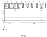
- FIG. 12 shows another example of the isolation region 204 .
- FIG. 13 shows another example of the isolation region 204 .
- FIG. 14 shows an example of the cross section g-g in FIG. 4 .
- FIG. 15 shows an example of the cross section h-h in FIG. 5 .
- FIG. 16 shows an example of the cross section h-h in FIG. 5 .
- FIG. 17 shows a partial process of a manufacturing method of the semiconductor device 100 .
- FIG. 18 illustrates an example of a lower end region forming step S 1704 .
- one side in a direction parallel to a depth direction of a semiconductor substrate is referred to as “upper” and the other side is referred to as “lower”.
- One surface of two principal surfaces of a substrate, a layer or other member is referred to as an upper surface, and the other surface is referred to as a lower surface.
- “Upper” and “lower” directions are not limited to a direction of gravity, or a direction in which a semiconductor device is mounted.
- orthogonal coordinate axes of an X axis, a Y axis, and a Z axis may be described using orthogonal coordinate axes of an X axis, a Y axis, and a Z axis.
- the orthogonal coordinate axes merely specify relative positions of components, and do not limit a specific direction.
- the Z axis is not limited to indicate a height direction with respect to the ground.
- a +Z axis direction and a ⁇ Z axis direction are directions opposite to each other.
- the Z axis direction is described without describing the signs, it means that the direction is parallel to the +Z axis and the ⁇ Z axis.
- orthogonal axes parallel to the upper surface and the lower surface of the semiconductor substrate are referred to as the X axis and the Y axis.
- an axis perpendicular to the upper surface and the lower surface of the semiconductor substrate is referred to as the Z axis.
- the direction of the Z axis may be referred to as the depth direction.
- a direction parallel to the upper surface and the lower surface of the semiconductor substrate may be referred to as a horizontal direction, including an X axis direction and a Y axis direction.
- a region from the center of the semiconductor substrate in the depth direction to the upper surface of the semiconductor substrate may be referred to as an upper surface side.
- a region from the center of the semiconductor substrate in the depth direction to the lower surface of the semiconductor substrate may be referred to as a lower surface side.
- a case where a term such as “same” or “equal” is mentioned may include a case where an error due to a variation in manufacturing or the like is included.
- the error is, for example, within 10%.
- a conductivity type of a doping region where doping has been carried out with an impurity is described as a P type or an N type.
- the impurity may particularly mean either a donor of the N type or an acceptor of the P type, and may be described as a dopant.
- doping means introducing the donor or the acceptor into the semiconductor substrate and turning it into a semiconductor presenting a conductivity type of the N type, or a semiconductor presenting a conductivity type of the P type.
- a doping concentration means a concentration of the donor or a concentration of the acceptor in a thermal equilibrium state.
- a net doping concentration means a net concentration obtained by adding the donor concentration set as a positive ion concentration to the acceptor concentration set as a negative ion concentration, taking into account of polarities of charges.
- the net doping concentration at any position is given as N D ⁇ N A .
- the net doping concentration may be simply referred to as the doping concentration.
- the donor has a function of supplying electrons to a semiconductor.
- the acceptor has a function of receiving electrons from the semiconductor.
- the donor and the acceptor are not limited to the impurities themselves.
- a VOH defect which is a combination of a vacancy (V), oxygen (O), and hydrogen (H) existing in the semiconductor functions as the donor that supplies electrons.
- the VOH defect may be referred to as a hydrogen donor.
- the bulk donor is a dopant donor substantially uniformly contained in an ingot during the manufacture of the ingot from which the semiconductor substrate is made.
- the bulk donor of this example is an element other than hydrogen.
- the dopant of the bulk donor is, for example, phosphorous, antimony, arsenic, selenium, or sulfur, but the present invention is not limited to these.
- the bulk donor of this example is phosphorous.
- the bulk donor is also contained in a region of the P type.
- the semiconductor substrate may be a wafer cut out from a semiconductor ingot, or may be a chip obtained by singulating the wafer.
- the semiconductor ingot may be manufactured by any one of a Czochralski method (CZ method), a magnetic field applied Czochralski method (MCZ method), or a float zone method (FZ method).
- CZ method Czochralski method
- MCZ method magnetic field applied Czochralski method
- FZ method float zone method
- the ingot of this example is manufactured by the MCZ method.
- An oxygen concentration contained in the substrate manufactured by the MCZ method is 1 ⁇ 10 17 to 7 ⁇ 10 17 /cm 3 .
- the oxygen concentration contained in the substrate manufactured by the FZ method is 1 ⁇ 10 15 to 5 ⁇ 10 16 /cm 3 .
- the bulk donor concentration may use a chemical concentration of bulk donors distributed throughout the semiconductor substrate, or may be a value from 90% to 100% of the chemical concentration.
- the bulk donor concentration (D0) of the non-doped substrate is, for example, from 1 ⁇ 10 10 /cm 3 or more and to 5 ⁇ 10 12 /cm 3 or less.
- the bulk donor concentration (D0) of the non-doped substrate is preferably 1 ⁇ 10 11 /cm 3 or more.
- the bulk donor concentration (D0) of the non-doped substrate is preferably 5 ⁇ 10 12 /cm 3 or less.
- Each concentration in the present invention may be a value at room temperature. As the value at room temperature, a value at 300 K (Kelvin) (about 26.9° C.) may be used as an example.
- a description of a P+ type or an N+ type means a higher doping concentration than that of the P type or the N type
- a description of a P ⁇ type or an N ⁇ type means a lower doping concentration than that of the P type or the N type
- a description of a P++ type or an N++ type means a higher doping concentration than that of the P+ type or the N+ type.
- a unit system is the SI base unit system unless otherwise particularly noted. Although a unit of length may be expressed in cm, calculations may be carried out after conversion to meters (m).
- a chemical concentration in the present specification indicates an atomic density of an impurity measured regardless of an electrical activation state.
- the chemical concentration can be measured by, for example, secondary ion mass spectrometry (SIMS).
- SIMS secondary ion mass spectrometry
- the net doping concentration described above can be measured by capacitance-voltage profiling (CV profiling).
- CV profiling capacitance-voltage profiling
- SRP method spreading resistance profiling
- the carrier concentration measured by the CV profiling or the SRP method may be a value in a thermal equilibrium state.
- the donor concentration is sufficiently higher than the acceptor concentration, and thus the carrier concentration of the region may be set as the donor concentration.
- the carrier concentration of the region may be set as the acceptor concentration.
- the doping concentration of the N type region may be referred to as the donor concentration
- the doping concentration of the P type region may be referred to as the acceptor concentration.
- a concentration of the donor, acceptor, or net doping when a concentration distribution of the donor, acceptor, or net doping has a peak in a region, a value of the peak may be set as the concentration of the donor, acceptor, or net doping in the region.
- concentration of the donor, acceptor or net doping is substantially uniform in a region, or the like, an average value of the concentration of the donor, acceptor or net doping in the region may be set as the concentration of the donor, acceptor or net doping.
- atoms/cm 3 or/cm 3 is used to indicate a concentration per unit volume. This unit is used for a concentration of a donor or an acceptor in a semiconductor substrate, or a chemical concentration. A notation of atoms may be omitted.
- the carrier concentration measured by the SRP method may be lower than the concentration of the donor or the acceptor.
- carrier mobility of the semiconductor substrate may be lower than a value in a crystalline state. The reduction in carrier mobility occurs when carriers are scattered due to disorder (disorder) of a crystal structure due to a lattice defect or the like.
- the concentration of the donor or the acceptor calculated from the carrier concentration measured by the CV profiling or the SRP method may be lower than a chemical concentration of an element indicating the donor or the acceptor.
- a donor concentration of phosphorous or arsenic serving as a donor, or an acceptor concentration of boron (boron) serving as an acceptor is approximately 99% of chemical concentrations of these.
- a donor concentration of hydrogen serving as a donor is approximately from 0.1% to 10% of a chemical concentration of hydrogen.
- FIG. 1 illustrates a top view showing an example of a semiconductor device 100 according to one embodiment of the present invention.
- FIG. 1 shows a position at which each member is projected on an upper surface of a semiconductor substrate 10 .
- FIG. 1 shows merely some members of the semiconductor device 100 , and omits illustrations of some members.
- the semiconductor device 100 includes the semiconductor substrate 10 .
- the semiconductor substrate 10 is a substrate that is formed of a semiconductor material.
- the semiconductor substrate 10 is a silicon substrate.
- the semiconductor substrate 10 has an end side 162 in the top view. When merely referred to as the top view in the present specification, it means that the semiconductor substrate 10 is viewed from an upper surface side.
- the semiconductor substrate 10 of this example has two sets of end sides 162 opposite to each other in the top view. In FIG. 1 , the X axis and the Y axis are parallel to any of the end sides 162 . In addition, the Z axis is perpendicular to the upper surface of the semiconductor substrate 10 .
- the semiconductor substrate 10 is provided with an active portion 160 .
- the active portion 160 is a region where a main current flows in the depth direction between the upper surface and a lower surface of the semiconductor substrate 10 when the semiconductor device 100 operates.
- An emitter electrode is provided above the active portion 160 , but is omitted in FIG. 1 .
- the active portion 160 may refer to a region that overlaps with the emitter electrode in the top view. In addition, a region sandwiched by the active portion 160 in the top view may also be included in the active portion 160 .
- the active portion 160 is provided with a transistor portion 70 including a transistor element such as an IGBT (Insulated Gate Bipolar Transistor).
- the active portion 160 may further be provided with a diode portion 80 including a diode element such as a freewheeling diode (FWD).
- FWD freewheeling diode
- the transistor portion 70 and the diode portion 80 are alternately arranged along a predetermined array direction (the X axis direction in this example) on the upper surface of the semiconductor substrate 10 .
- the semiconductor device 100 of this example is a reverse-conducting IGBT (RC-IGBT).
- a region where each of the transistor portions 70 is arranged is indicated by a symbol “I”, and a region where each of the diode portions 80 is arranged is indicated by a symbol “F”.
- a direction perpendicular to the array direction in a top view may be referred to as an extending direction (the Y axis direction in FIG. 1 ).
- Each of the transistor portions 70 and the diode portions 80 may have a longitudinal length in the extending direction. In other words, the length of each of the transistor portions 70 in the Y axis direction is greater than the width in the X axis direction.
- each of the diode portions 80 in the Y axis direction is greater than the width in the X axis direction.
- the extending direction of the transistor portion 70 and the diode portion 80 , and a longitudinal direction of each trench portion which will be described below may be the same.
- Each of the diode portions 80 includes a cathode region of N+ type in a region in contact with the lower surface of the semiconductor substrate 10 .
- a region where the cathode region is provided is referred to as the diode portion 80 .
- the diode portion 80 is a region that overlaps with the cathode region in the top view.
- a collector region of the P+ type may be provided in a region other than the cathode region.
- the diode portion 80 may also include an extension region 81 where the diode portion 80 extends to a gate runner to be described later in the Y axis direction. The collector region is provided on a lower surface of the extension region 81 .
- the transistor portion 70 has the collector region of the P+ type in a region in contact with the lower surface of the semiconductor substrate 10 . Further, in the transistor portion 70 , an emitter region of the N type, a base region of the P type, and a gate structure having a gate conductive portion and a gate dielectric film are periodically arranged on the upper surface side of the semiconductor substrate 10 .
- the semiconductor device 100 may have one or more pads above the semiconductor substrate 10 .
- the semiconductor device 100 of this example has a gate pad 164 .
- the semiconductor device 100 may have a pad such as an anode pad, a cathode pad, and a current detection pad.
- Each pad is arranged in a region close to the end side 162 .
- the region close to the end side 162 refers to a region between the end side 162 and the emitter electrode in the top view.
- each pad may be connected to an external circuit via a wiring such as a wire.
- a gate potential is applied to the gate pad 164 .
- the gate pad 164 is electrically connected to a conductive portion of a gate trench portion of the active portion 160 .
- the semiconductor device 100 includes a gate runner that connects the gate pad 164 and the gate trench portion. In FIG. 1 , the gate runner is hatched with diagonal lines.
- the gate runner of the present example includes an outer circumferential gate runner 130 and an active-side gate runner 131 .
- the outer circumferential gate runner 130 is arranged between the active portion 160 and the end side 162 of the semiconductor substrate 10 in the top view.
- the outer circumferential gate runner 130 of the present example encloses the active portion 160 in the top view.
- a region enclosed by the outer circumferential gate runner 130 in the top view may be the active portion 160 .
- a well region is formed below the gate runner.
- the well region is a region of the P type having a higher concentration than the base region described below, and is formed to a position deeper than the base region from the upper surface of the semiconductor substrate 10 .
- a region surrounded by the well region in the top view may be the active portion 160 .
- the outer circumferential gate runner 130 is connected to the gate pad 164 .
- the outer circumferential gate runner 130 is arranged above the semiconductor substrate 10 .
- the outer circumferential gate runner 130 may be a metal wiring containing aluminum or the like.
- the active-side gate runner 131 is provided in the active portion 160 . Providing the active-side gate runner 131 in the active portion 160 can reduce a variation in wiring length from the gate pad 164 for each region of the semiconductor substrate 10 .
- the outer circumferential gate runner 130 and the active-side gate runner 131 are connected to the gate trench portion of the active portion 160 .
- the outer circumferential gate runner 130 and the active-side gate runner 131 are arranged above the semiconductor substrate 10 .
- the outer circumferential gate runner 130 and the active-side gate runner 131 may be a wiring formed of a semiconductor such as polysilicon doped with an impurity.
- the active-side gate runner 131 may be connected to the outer circumferential gate runner 130 .
- the active-side gate runner 131 of this example is provided extending in the X axis direction so as to cross the active portion 160 from one outer circumferential gate runner 130 to the other outer circumferential gate runner 130 sandwiching the active portion 160 , substantially at the center of the Y axis direction.
- the transistor portion 70 and the diode portion 80 may be alternately arranged in the X axis direction in each of the divided regions.
- the semiconductor device 100 may include a temperature sensing portion (not shown) which is a PN junction diode formed of polysilicon or the like, and a current detection portion (not shown) which simulates an operation of the transistor portion provided in the active portion 160 .
- the semiconductor device 100 of this example includes an edge termination structure portion 90 between the active portion 160 and the end side 162 in the top view.
- the edge termination structure portion 90 of this example is arranged between the outer circumferential gate runner 130 and the end side 162 .
- the edge termination structure portion 90 reduces an electric field strength on the upper surface side of the semiconductor substrate 10 .
- the edge termination structure portion 90 may include at least one of a guard ring, a field plate, or a RESURF annularly provided to enclose the active portion 160 .
- FIG. 2 is an enlarged drawing of a region D in FIG. 1 .
- the region D is a region including the transistor portion 70 , the diode portion 80 , and the active-side gate runner 131 .
- the semiconductor device 100 of this example includes a gate trench portion 40 , a dummy trench portion 30 , a well region 11 , an emitter region 12 , a base region 14 , and a contact region 15 which are provided inside on the upper surface side of the semiconductor substrate 10 .
- the gate trench portion 40 and the dummy trench portion 30 each are an example of the trench portion.
- the semiconductor device 100 of the present example includes an emitter electrode 52 and the active-side gate runner 131 which are provided above the upper surface of the semiconductor substrate 10 .
- the emitter electrode 52 and the active-side gate runner 131 are provided separate from each other.
- an interlayer dielectric film is provided, but an illustration thereof is omitted in FIG. 2 .
- a contact hole 54 is provided passing through the interlayer dielectric film.
- each contact hole 54 is hatched with the diagonal lines.
- the emitter electrode 52 is provided above the gate trench portion 40 , the dummy trench portion 30 , the well region 11 , the emitter region 12 , the base region 14 , and the contact region 15 .
- the emitter electrode 52 is in contact with the emitter region 12 , the contact region 15 , and the base region 14 on the upper surface of the semiconductor substrate 10 , through the contact hole 54 .
- the emitter electrode 52 is connected to a dummy conductive portion in the dummy trench portion 30 through a contact hole provided in the interlayer dielectric film.
- the emitter electrode 52 may be connected to the dummy conductive portion of the dummy trench portion 30 at an edge of the dummy trench portion 30 in the Y axis direction or the like.
- the dummy conductive portion of the dummy trench portion 30 may not be connected to the emitter electrode 52 and the gate conductive portion, and may be controlled to have a different potential from a potential of the emitter electrode 52 and a potential of the gate conductive portion.
- the active-side gate runner 131 is connected to the gate trench portion 40 through the contact hole provided in the interlayer dielectric film.
- the active-side gate runner 131 may be connected to a gate conductive portion of the gate trench portion 40 in an edge portion 41 of the gate trench portion 40 in the Y axis direction.
- the active-side gate runner 131 is not connected to the dummy conductive portion in the dummy trench portion 30 .
- the emitter electrode 52 is formed of a material including metal.
- FIG. 2 shows a range where the emitter electrode 52 is provided.
- at least a part of a region of the emitter electrode 52 is formed of aluminum or an aluminum-silicon alloy, for example, a metal alloy such as AlSi or AlSiCu.
- the emitter electrode 52 may have a barrier metal formed of titanium, a titanium compound, or the like below a region formed of aluminum or the like. Further, a plug, which is formed by embedding tungsten or the like so as to be in contact with the barrier metal and aluminum or the like, may be included in the contact hole.
- the well region 11 is provided so as to overlap with the active-side gate runner 131 .
- the well region 11 is provided so as to extend with a predetermined width also in a range not overlapping with the active-side gate runner 131 .
- the well region 11 of this example is provided away from an end of the contact hole 54 in the Y axis direction toward the active-side gate runner 131 side.
- the well region 11 is a second conductivity type region having a higher doping concentration than the base region 14 .
- the base region 14 of the present example is of the P ⁇ type, and the well region 11 is of the P+ type.
- Each of the transistor portion 70 and the diode portion 80 includes a plurality of trench portions arranged in the array direction.
- the transistor portion 70 of the present example one or more gate trench portions 40 and one or more dummy trench portions 30 are alternately provided along the array direction.
- the diode portion 80 of the present example the plurality of dummy trench portions 30 are provided along the array direction.
- the gate trench portion 40 is not provided.
- the gate trench portion 40 of the present example may have two linear portions 39 extending along the extending direction perpendicular to the array direction (portions of a trench that are linear along the extending direction), and the edge portion 41 connecting the two linear portions 39 .
- the extending direction in FIG. 2 is the Y axis direction.
- At least a part of the edge portion 41 is preferably provided in a curved shape in a top view.
- the dummy trench portions 30 are provided between the respective linear portions 39 of the gate trench portions 40 . Between the respective linear portions 39 , one dummy trench portion 30 may be provided, or a plurality of dummy trench portions 30 may be provided.
- the dummy trench portion 30 may have a linear shape extending in the extending direction, or may have linear portions 29 and an edge portion 31 similar to the gate trench portion 40 .
- the semiconductor device 100 shown in FIG. 2 includes both of the linear dummy trench portion 30 having no edge portion 31 , and the dummy trench portion 30 having the edge portion 31 .
- a diffusion depth of the well region 11 may be deeper than the depth of the gate trench portion 40 and the dummy trench portion 30 .
- the end portions in the Y axis direction of the gate trench portion 40 and the dummy trench portion 30 are provided in the well region 11 in a top view. In other words, the bottom of each trench portion in the depth direction is covered with the well region 11 at the end portion of each trench portion in the Y axis direction. With this configuration, the electric field strength on the bottom portion of each trench portion can be reduced.
- a mesa portion is provided between the respective trench portions in the array direction.
- the mesa portion refers to a region sandwiched between the trench portions inside the semiconductor substrate 10 .
- an upper end of the mesa portion is the upper surface of the semiconductor substrate 10 .
- the depth position of the lower end of the mesa portion is the same as the depth position of the lower end of the trench portion.
- the mesa portion of the present example is provided so as to extend in the extending direction (the Y axis direction) along the trench, on the upper surface of the semiconductor substrate 10 .
- a mesa portion 60 is provided in the transistor portion 70
- a mesa portion 61 is provided in the diode portion 80 .
- the portion refers to each of the mesa portion 60 and the mesa portion 61 .
- Each mesa portion is provided with the base region 14 .
- a region arranged closest to the active-side gate runner 131 , in the base region 14 exposed on the upper surface of the semiconductor substrate 10 is to be a base region 14 - e .
- FIG. 2 shows the base region 14 - e arranged at one end portion of each mesa portion in the extending direction, the base region 14 - e is also arranged at the other end portion of each mesa portion.
- at least one of the emitter region 12 of the first conductivity type or the contact region 15 of the second conductivity type may be provided in the region sandwiched between the base regions 14 - e in a top view.
- the emitter region 12 of this example is an N+ type
- the contact region 15 is a P+ type.
- the emitter region 12 and the contact region 15 may be provided between the base region 14 and the upper surface of the semiconductor substrate 10 in the depth direction.
- the mesa portion 60 of the transistor portion 70 includes the emitter region 12 exposed on the upper surface of the semiconductor substrate 10 .
- the emitter region 12 is provided in contact with the gate trench portion 40 .
- the mesa portion 60 in contact with the gate trench portion 40 may be provided with the contact region 15 exposed on the upper surface of the semiconductor substrate 10 .
- Each of the contact region 15 and the emitter region 12 in the mesa portion 60 is provided from one trench portion to the other trench portion in the X axis direction.
- the contact region 15 and the emitter region 12 of the mesa portion 60 are alternately arranged along the extending direction of the trench portion (the Y axis direction).
- the contact region 15 and the emitter region 12 of the mesa portion 60 may be provided in a stripe pattern along the extending direction of the trench portion (the Y axis direction).
- the emitter region 12 is provided in a region in contact with the trench portion, and the contact region 15 is provided in a region sandwiched between the emitter regions 12 .
- the emitter region 12 is not provided in the mesa portion 61 of the diode portion 80 .
- the base region 14 and the contact region 15 may be provided on an upper surface of the mesa portion 61 .
- the contact region 15 may be provided in contact with each of the base regions 14 - e in a region sandwiched between the base regions 14 - e on the upper surface of the mesa portion 61 .
- the base region 14 may be provided in a region sandwiched between the contact regions 15 on the upper surface of the mesa portion 61 .
- the base region 14 may be arranged in the entire region sandwiched between the contact regions 15 .
- the contact hole 54 is provided above each mesa portion.
- the contact hole 54 is arranged in the region sandwiched between the base regions 14 - e .
- the contact hole 54 of this example is provided above respective regions of the contact region 15 , the base region 14 , and the emitter region 12 .
- the contact hole 54 is not provided in regions corresponding to the base region 14 - e and the well region 11 .
- the contact hole 54 may be arranged at the center of the mesa portion 60 in the array direction (the X axis direction).
- a cathode region 82 of the N+ type is provided in a region in direct contact with the lower surface of the semiconductor substrate 10 .
- a collector region 22 of the P+ type may be provided in a region where the cathode region 82 is not provided.
- the cathode region 82 and the collector region 22 are provided between the lower surface 23 of the semiconductor substrate 10 and a buffer region 20 .
- a boundary between the cathode region 82 and the collector region 22 is indicated by a dotted line.
- the cathode region 82 is arranged apart from the well region 11 in the Y axis direction. With this configuration, a distance between the P type region (the well region 11 ) which has a relatively high doping concentration and is formed to a deep position and the cathode region 82 is ensured, so that the breakdown voltage can be improved.
- the end portion in the Y axis direction of the cathode region 82 of this example is arranged farther away from the well region 11 than the end portion in the Y axis direction of the contact hole 54 .
- the end portion in the Y axis direction of the cathode region 82 may be arranged between the well region 11 and the contact hole 54 .
- FIG. 3 is a drawing showing an example of a cross section e-e in FIG. 2 .
- the cross section e-e is an XZ plane passing through the emitter region 12 and the cathode region 82 .
- the semiconductor device 100 of this example includes the semiconductor substrate 10 , the interlayer dielectric film 38 , the emitter electrode 52 , and the collector electrode 24 in the cross section.
- the interlayer dielectric film 38 is provided on the upper surface of the semiconductor substrate 10 .
- the interlayer dielectric film 38 is a film including at least one layer of a dielectric film such as silicate glass to which an impurity such as boron or phosphorous is added, a thermal oxide film, and other dielectric films.
- the interlayer dielectric film 38 is provided with the contact hole 54 described in FIG. 2 .
- the emitter electrode 52 is provided on the upper side of the interlayer dielectric film 38 .
- the emitter electrode 52 is in contact with an upper surface 21 of the semiconductor substrate 10 through the contact hole 54 of the interlayer dielectric film 38 .
- the collector electrode 24 is provided on a lower surface 23 of the semiconductor substrate 10 .
- the emitter electrode 52 and the collector electrode 24 are formed of a metal material such as aluminum.
- the direction in which the emitter electrode 52 is connected to the collector electrode 24 (the z axis direction) is referred to as a depth direction.
- the semiconductor substrate 10 includes an N type or N ⁇ type drift region 18 .
- the drift region 18 is provided in each of the transistor portion 70 and the diode portion 80 .
- an N+ type of emitter region 12 and a P ⁇ type of base region 14 are provided in order from an upper surface 21 side of the semiconductor substrate 10 .
- the drift region 18 is provided below the base region 14 .
- the mesa portion 60 may be provided with an N+ type accumulation region 16 .
- the accumulation region 16 is arranged between the base region 14 and the drift region 18 .
- the emitter region 12 is exposed on the upper surface 21 of the semiconductor substrate 10 and is provided in contact with the gate trench portion 40 .
- the emitter region 12 may be in contact with the trench portions on both sides of the mesa portion 60 .
- the emitter region 12 has a higher doping concentration than the drift region 18 .
- the base region 14 is provided below the emitter region 12 .
- the base region 14 of this example is provided in contact with the emitter region 12 .
- the base region 14 may be in contact with the trench portions on both sides of the mesa portion 60 .
- the accumulation region 16 is provided below the base region 14 .
- the accumulation region 16 is an N+ type region having a higher doping concentration than the drift region 18 . That is, the accumulation region 16 has a higher donor concentration than the drift region 18 .
- IE effect carrier injection enhancement effect
- the accumulation region 16 may be provided to cover an entire lower surface of the base region 14 in each mesa portion 60 .
- the mesa portion 61 of the diode portion 80 is provided with the P ⁇ type of base region 14 in contact with the upper surface 21 of the semiconductor substrate 10 .
- the drift region 18 is provided below the base region 14 .
- the accumulation region 16 may be provided below the base region 14 .
- an N+ type buffer region 20 may be provided below the drift region 18 .
- the doping concentration of the buffer region 20 is higher than the doping concentration of the drift region 18 .
- the buffer region 20 may have a concentration peak having a higher doping concentration than the drift region 18 .
- the doping concentration of the concentration peak indicates a doping concentration at the local maximum of the concentration peak.
- an average value of doping concentrations in the region where the doping concentration distribution is substantially flat may be used as the doping concentration of the drift region 18 .
- the buffer region 20 may have two or more concentration peaks in the depth direction (Z axis direction) of the semiconductor substrate 10 .
- the concentration peak of the buffer region 20 may be provided at the same depth position as, for example, a chemical concentration peak of hydrogen (a proton) or phosphorous.
- the buffer region 20 may function as a field stopper layer which prevents a depletion layer expanding from the lower end of the base region 14 from reaching the collector region 22 of the P+ type and the cathode region 82 of the N+ type.
- the collector region 22 of the P+ type is provided below the buffer region 20 .
- An acceptor concentration of the collector region 22 is higher than an acceptor concentration of the base region 14 .
- the collector region 22 may include an acceptor which is the same as or different from an acceptor of the base region 14 .
- the acceptor of the collector region 22 is, for example, boron.
- the cathode region 82 of the N+ type is provided below the buffer region 20 in the diode portion 80 .
- a donor concentration of the cathode region 82 is higher than a donor concentration of the drift region 18 .
- a donor of the cathode region 82 is, for example, hydrogen or phosphorous. Note that an element serving as a donor and an acceptor in each region is not limited to the above-described example.
- the collector region 22 and the cathode region 82 are exposed on the lower surface 23 of the semiconductor substrate 10 and are connected to the collector electrode 24 .
- the collector electrode 24 may be in contact with the entire lower surface 23 of the semiconductor substrate 10 .
- the emitter electrode 52 and the collector electrode 24 are formed of a metal material such as aluminum.
- One or more gate trench portions 40 and one or more dummy trench portions 30 are provided on the upper surface 21 side of the semiconductor substrate 10 .
- Each trench portion passes through the base region 14 from the upper surface 21 of the semiconductor substrate 10 , and is provided to below the base region 14 .
- each trench portion also passes through the doping regions of these.
- the configuration of the trench portion penetrating through the doping region is not limited to that manufactured in the order of forming the doping region and then forming the trench portion.
- the configuration of the trench portion passing through the doping region includes a configuration of the doping region being formed between the trench portions after forming the trench portion.
- the transistor portion 70 is provided with the gate trench portion 40 and the dummy trench portion 30 .
- the dummy trench portion 30 is provided, and the gate trench portion 40 is not provided.
- the boundary in the X axis direction between the diode portion 80 and the transistor portion 70 in this example is the boundary between the cathode region 82 and the collector region 22 .
- the gate trench portion 40 includes a gate trench provided in the upper surface 21 of the semiconductor substrate 10 , a gate dielectric film 42 , and a gate conductive portion 44 .
- the gate dielectric film 42 is provided to cover the inner wall of the gate trench.
- the gate dielectric film 42 may be formed by oxidizing or nitriding a semiconductor on the inner wall of the gate trench.
- the gate conductive portion 44 is provided inside from the gate dielectric film 42 in the gate trench. That is, the gate dielectric film 42 insulates the gate conductive portion 44 from the semiconductor substrate 10 .
- the gate conductive portion 44 is formed of a conductive material such as polysilicon.
- the gate conductive portion 44 may be provided longer than the base region 14 in the depth direction.
- the gate trench portion 40 in the cross section is covered by the interlayer dielectric film 38 on the upper surface 21 of the semiconductor substrate 10 .
- the gate conductive portion 44 is electrically connected to the gate runner. When a predetermined gate voltage is applied to the gate conductive portion 44 , a channel is formed by an electron inversion layer in a surface layer of the base region 14 at a boundary in contact with the gate trench portion 40 .
- the dummy trench portions 30 may have the same structure as those of the gate trench portions 40 in the cross section.
- the dummy trench portion 30 includes a dummy trench provided in the upper surface 21 of the semiconductor substrate 10 , a dummy dielectric film 32 , and a dummy conductive portion 34 .
- the dummy conductive portion 34 is electrically connected to the emitter electrode 52 .
- the dummy dielectric film 32 is provided covering an inner wall of the dummy trench.
- the dummy conductive portion 34 is provided in the dummy trench, and is provided inside the dummy dielectric film 32 .
- the dummy dielectric film 32 insulates the dummy conductive portion 34 from the semiconductor substrate 10 .
- the dummy conductive portion 34 may be formed of the same material as that of the gate conductive portion 44 .
- the dummy conductive portion 34 is formed of a conductive material such as polysilicon or the like.
- the dummy conductive portion 34 may have the same length as that of the gate conductive portion 44 in the depth direction.
- the gate trench portion 40 and the dummy trench portion 30 of this example are covered with the interlayer dielectric film 38 on the upper surface 21 of the semiconductor substrate 10 .
- the bottoms of the dummy trench portion 30 and the gate trench portion 40 may be formed in a curved-surface shape (a curved shape in the cross section) convexly downward.
- a depth position of a lower end of the gate trench portion 40 is set as Zt.
- the semiconductor device 100 of the present example includes a P type first lower end region 202 which is provided to be in contact with the lower end of the trench portion.
- a doping concentration of the first lower end region 202 may be equal to or less than a doping concentration of the base region 14 .
- a doping concentration of the first lower end region 202 of the present example is lower than a doping concentration of the base region 14 .
- a P type dopant may be boron or may be aluminum.
- the first lower end region 202 is arranged apart from the base region 14 .
- An N type region (in the present example, at least one of the accumulation region 16 or the drift region 18 ) is provided between the first lower end region 202 and the base region 14 .
- the first lower end regions 202 are provided in series to be in contact with the lower end of two or more trench portions in an X axis direction. That is, the first lower end region 202 is provided to cover a mesa portion between the trench portions. The first lower end region 202 may cover a plurality of mesa portions. The first lower end region 202 of the present example is provided to be in contact with the lower end of each of the two or more trench portions including the gate trench portion 40 .
- the first lower end region 202 may be in contact with the lower end of each of the two or more trench portions in the respective transistor portions 70 . Also, the first lower end region 202 may be in contact with the lower end of each of the two or more gate trench portions 40 in the respective transistor portions 70 . The first lower end region 202 may be in contact with the lower end of each of the two or more dummy trench portions 30 in the respective transistor portions 70 . The first lower end region 202 may be in contact with the lower end of each of all the trench portions in at least one transistor portion 70 . Also, the first lower end region 202 may be in contact with the lower end of each of all the gate trench portions 40 in at least one transistor portion 70 .
- the first lower end region 202 may be in contact with the lower end of each of the two or more trench portions in the respective diode portions 80 .
- the first lower end region 202 may be in contact with the lower end of each of all the trench portions in at least one diode portion 80 .
- the first lower end region 202 is provided to extend in a Y axis direction.
- a length of the first lower end region 202 in the Y axis direction is shorter than a length of the trench portion in the Y axis direction.
- the length of the first lower end region 202 in the Y axis direction may be 50% or more, may be 70% or more, may be 90% or more of the length of the trench portion in the Y axis direction.
- the first lower end region 202 By providing the first lower end region 202 , a potential increase near the lower end of the trench portion when the semiconductor device 100 is turned on can be suppressed. Thus, it is possible to reduce a slope (dv/dt) of a waveform of emitter-collector voltage at the time of turn-on and to reduce noise in a voltage or current waveform at the time of switching.
- a potential of the first lower end region 202 is different from a potential of the emitter electrode 52 .
- the first lower end region 202 is arranged, in a Z axis direction, apart from the base region 14 which is connected to the emitter electrode 52 .
- the first lower end region 202 is arranged, in a top view, apart from the well region which is connected to the emitter electrode 52 .
- the active portion 160 may have a portion to which the first lower end region 202 is not provided in at least one of the X axis direction or the Y axis direction.
- the first lower end region 202 may be an electrically floating region to which no electrode is connected.
- FIG. 4 shows an exemplary arrangement of a well region 11 and a first lower end region 202 in a top view.
- the first lower end region 202 of the present example is provided in the active portion 160 .
- the first lower end region 202 may be provided in an area of 50% or more, may be provided in an area of 70% or more, or may be provided in an area of 90% or more of the active portion 160 in a top view.
- the well region 11 is provided below the gate runner shown in the FIG. 1 .
- the well region 11 and the first lower end region 202 are arranged in different locations.
- the well region 11 may be arranged to surround the first lower end region 202 .
- the well region 11 may surround the respective first lower end regions 202 .
- an isolation region 204 is provided between the well region 11 and the first lower end region 202 .
- the isolation region 204 includes an N type region which separates the well region 11 and the first lower end region 202 .
- the N type region is, for example, a drift region 18 .
- the N type region is arranged to surround the first lower end region 202 in a top view.
- the well region 11 is arranged to surround the isolation region 204 in a top view.
- the isolation region 204 is hatched with diagonal lines.
- the isolation region 204 is provided in the entire area in the active portion 160 in which the first lower end region 202 is not provided. Note that when there exists a portion inside the active portion 160 in which the first lower end region 202 is not provided, the portion may also be provided with the isolation region 204 .
- the isolation region 204 arranged inside the active portion 160 may be surrounded by the first lower end region 202 in a top view.
- FIG. 5 shows an example of a cross section f-f in FIG. 4 .
- the cross section f-f is an XZ plane which passes through the first lower end region 202 , the isolation region 204 and the well region 11 . That is, the cross section f-f is the XZ plane in the vicinity of a boundary between the active portion 160 and the well region 11 .
- FIG. 5 shows a structure of the semiconductor substrate 10 and omits components such as an electrode and a dielectric film arranged above and below the semiconductor substrate 10 .
- FIG. 5 shows the gate trench portion 40 with a symbol G and the dummy trench portion 30 with a symbol E.
- the cross section f-f shown in FIG. 5 includes a transistor portion 70 which is arranged at the endmost in the X axis direction among a plurality of transistor portions 70 .
- a structure of the transistor portion 70 is similar to that of the transistor portion 70 described in FIG. 2 and FIG. 3 .
- one dummy trench portion 30 is arrayed between two gate trench portions 40 as G/E/G/E/ . . .
- two dummy trench portions 30 may be arrayed between two gate trench portions 40 as G/E/E/G/E/E/ . . .
- An array of the gate trench portions 40 and the dummy trench portions 30 may have another structure.
- a plurality of trench portions of the isolation region 204 may be arranged with a constant interval in the X axis direction. The interval between the trench portions of the isolation region 204 may be the same as the interval between the trench portions of the transistor portion 70 .
- the first lower end region 202 is provided at the lower end of the trench portion of the transistor portion 70 .
- a center of the gate trench portion 40 (G) arranged at the end in the X axis direction among the gate trench portions 40 (G) provided in direct contact with the emitter regions 12 is defined as an end portion of the transistor portion 70 in the X axis direction.
- the first lower end region 202 may extend outward farther than the transistor portion 70 in the X axis direction. That is, the first lower end region 202 may extend to a region in which a gate structure including the gate trench portion 40 and the emitter region 12 is not provided.
- the well region 11 is provided from the upper surface 21 of the semiconductor substrate 10 to below the base region 14 .
- the well region 11 is a region of a P+ type having a higher doping concentration than the base region 14 .
- a region between the first lower end region 202 and the well region 11 in a top view is referred to as an isolation region 204 .
- the isolation region 204 is provided with one or more trench portions.
- the isolation region 204 of the present example is provided with one or more gate trench portions 40 and one or more dummy trench portions 30 .
- the arrangement of the trench portions of the isolation region 204 in the X axis direction may be the same as or may be different from that of the transistor portion 70 .
- Each mesa portion of the isolation region 204 is provided with the base region 14 .
- the contact region 15 may be provided between the base region 14 and the upper surface 21 of the semiconductor substrate 10 .
- the emitter region 12 may be provided between the base region 14 and the upper surface 21 of the semiconductor substrate 10 .
- the mesa portion of the isolation region 204 may be provided with or may not be provided with an accumulation region 16 .
- the accumulation region 16 may be provided in one or more mesa portions located to be the closest to the transistor portion 70 among the mesa portions of the isolation region 204 .
- the first lower end region 202 of the present example is a P type region having a doping concentration lower than that of the well region 11 .
- the first lower end region 202 is arranged in at least a partial region of the transistor portion 70 .
- the first lower end region 202 of the present example extends closer to the well region 11 than the end portion of the transistor portion 70 .
- the first lower end region 202 may be terminated at the end portion of the transistor portion 70 or may be terminated inside the transistor portion 70 .
- the isolation region 204 has one or more second lower end regions 205 .
- the second lower end region 205 is a second conductivity type region provided to be in contact with the lower ends of one or more trench portions each including a gate trench portion 40 .
- a doping concentration of the second lower end region 205 may be higher than, may be lower than, or may be the same as that of the first lower end region 202 .
- the second lower end regions 205 may be provided in series along an extending direction of the trench portion (the Y axis direction).
- a length of the second lower end region 205 in the Y axis direction may be the same as a length of the first lower end region 202 in the Y axis direction, or may be 80% or more or 120% or less of a length of the first lower end region 202 in the Y axis direction.
- the second lower end region 205 may be provided discretely along the extending direction of the trench portion (the Y axis direction).
- the second lower end region 205 is provided between the first lower end region 202 and the well region 11 in a top view.
- the second lower end region 205 of the present example is provided between the first lower end region 202 and the well region 11 in the X axis direction.
- the second lower end region 205 is provided to be separated from the first lower end region 202 and the well region 11 .
- An N type region such as a drift region 18 is provided between the second lower end region 205 and the first lower end region 202 in a top view.
- An N type region such as a drift region 18 is provided between the second lower end region 205 and the well region 11 in a top view.
- an N type region such as a drift region 18 is provided between two second lower end regions 205 in a top view.
- a distance between the first lower end region 202 and the second lower end region 205 may be greater than or may be less than a width of the mesa portion in the isolation region 204 . Also, in the X axis direction, a distance between adjacent two second lower end regions 205 may be greater than or may be less than a width of the mesa portion in the isolation region 204 .
- a distance between the well region 11 and the second lower end region 205 may be greater than or may be less than a width of the mesa portion in the isolation region 204 .
- a potential of the second lower end region 205 is different from a potential of the emitter electrode 52 .
- the second lower end region 205 is arranged, in the Z axis direction, apart from the base region 14 which is connected to the emitter electrode 52 . Also, the second lower end region 205 is arranged, in a top view, apart from the well region 11 which is connected to the emitter electrode 52 .
- the second lower end region 205 may be an electrically floating region to which no electrode is connected.
- the first lower end region 202 by providing the first lower end region 202 , a potential increase near the lower end of the trench portion when the semiconductor device 100 is turned on can be suppressed. Thus, it is possible to reduce a slope (dv/dt) of a waveform of emitter-collector voltage at the time of turn-on and to reduce noise in a voltage or current waveform at the time of switching. Also, by providing the isolation region 204 , the first lower end region 202 and the well region 11 can be separated from each other, and the transistor portion 70 and the diode portion 80 can be operated.
- an imbalance occurs between an electric field near the lower end of the trench portion of a region in which the first lower end region 202 exists and an electric field near the lower end of the trench portion of a region in which the first lower end region 202 does not exist.
- an electric field strength near the lower end of the gate trench portion 40 where the first lower end region 202 is not provided an avalanche can easily be generated and a clamp withstand capability and a latch-up resistance decrease.
- the second lower end region 205 is provided at the lower end of at least one of the gate trench portion 40 in the isolation region 204 .
- the electric field strength near the lower end of the gate trench portion 40 of the isolation region 204 can be relaxed.
- the breakdown voltage or the withstand capability of the semiconductor device 100 can be improved.
- the second lower end region 205 may be provided for each of two or more gate trench portions 40 of the isolation region 204 . Each of the second lower end regions 205 is separated from each other. In the example of FIG. 5 , the second lower end region 205 is provided at the lower end of each of all the gate trench portions 40 in the isolation region 204 . In the present example, each second lower end region 205 is in contact with the lower end of one of the gate trench portions 40 and not in contact with the lower end of another one of the gate trench portions 40 other than the above-described one of the gate trench portions 40 . In the example of FIG. 5 , each second lower end region 205 is in contact with the lower end of one of the gate trench portions 40 , and not in contact with the lower end of the other trench portions.
- a width of the second lower end region 205 in the X axis direction may be less than, may be the same as, or may be larger than a width of the gate trench portion 40 in the X axis direction.
- the second lower end region 205 preferably covers the lowest part of the gate trench portion 40 (for example, the bottom surface of the gate trench portion 40 ).
- the second lower end region 205 may have a portion which is provided at a same depth position as the first lower end region 202 . That is, a range in the Z axis direction in which the second lower end region 205 is provided and a range in the Z axis direction in which the first lower end region 202 is provided may at least partially overlap. At least one of the drift region 18 or the accumulation region 16 may be arranged between the second lower end region 205 and the base region 14 .
- FIG. 6 shows another array example of the gate trench portion 40 and the dummy trench portion 30 .
- the active portion 160 of the present example is provided with two dummy trench portions 30 between two gate trench portions 40 .
- the gate trench portions 40 are not arranged in series in the X axis direction. That is, one gate trench portion 40 and two dummy trench portions 30 are alternately arranged.
- Other structures are similar to those in the examples described in FIG. 1 to FIG. 5 .
- the one or more gate trench portions 40 of the isolation region 204 are provided with the second lower end region 205 .
- the number of trench portions in contact with one of the second lower end regions 205 is less than the number of trench portions in contact with one of the first lower end regions 202 .
- the number of trench portions in contact with one of the second lower end regions 205 is 1, one of the first lower end regions 202 is in contact with a plurality of trench portions.
- One of the first lower end regions 202 may be in contact with lower ends of a plurality of gate trench portions 40 and a plurality of dummy trench portions 30 .
- FIG. 7 shows a distribution example of an electric field at a depth position of the lower end of the trench portion in an X axis direction.
- FIG. 7 shows an electric field distribution when a transistor portion 70 in which a current five times or more (six times in the present example) of the rated current flows is turned off.
- FIG. 7 shows a position of the lower end of the gate trench portion 40 in the X axis direction with a symbol G, and shows a position of the lower end of the dummy trench portion 30 in the X axis direction with a symbol E. Also, it schematically shows positions in the X axis direction in which the first lower end region 202 and the second lower end region 205 are provided. Note that the solid lines in FIG.
- the electric field at the lower end of the trench portion which is not covered by the first lower end region 202 increases.
- the electric field strength at the lower end of the gate trench portion 40 (G) significantly increases.
- an avalanche can easily be generated and a clamp withstand capability and a latch-up resistance decrease.
- the electric field near the lower end of the gate trench portion 40 can be decreased.
- the breakdown voltage and the withstand capability of the semiconductor device 100 can be improved.
- FIG. 8 shows another example of the second lower end region 205 .
- the second lower end region 205 of the present example is in contact with the lower end of one of the gate trench portions 40 , and is in contact with the lower end of the dummy trench portion 30 which is arranged adjacent to the gate trench portion 40 in the X axis direction.
- the second lower end region 205 is in contact with the lower end of one of the gate trench portions 40 , and in contact with the lower ends of two dummy trench portions 30 with the gate trench portion 40 sandwiched therebetween in the X axis direction.
- At least a portion below the mesa portion 60 which is sandwiched by two adjacent dummy trench portions 30 is not provided with the second lower end region 205 .
- two second lower end regions 205 provided at the two adjacent dummy trench portions 30 are separated from each other.
- an N type region is provided between the separated two second lower end region 205 .
- the N type region is, for example, a drift region 18 .
- FIG. 9 A is an enlarged drawing showing a region near the first lower end region 202 and the second lower end region 205 .
- the second lower end region 205 of the present example is in contact with the lower end of a plurality of trench portions.
- a doping concentration of the second lower end region 205 at the lower end of the gate trench portion 40 is referred to as Dg.
- the doping concentration Dg may be the maximum value or may be an average value obtained by dividing an integrated value I D g of a doping concentration of the second lower end region 205 on a line m-m which passes through the lowest point of the gate trench portion 40 and which is parallel to the Z axis, with a width T2 of a depth direction to the lower end from the upper end of the second lower end region 205 .
- a doping concentration of the second lower end region 205 at the lower end of the dummy trench portion 30 is referred to as Dd.
- the doping concentration Dd may be an average value or may be the maximum value obtained by dividing an integrated value I D d of a doping concentration of the second lower end region 205 on a line k-k which passes through the lowest point of the dummy trench portion 30 and which is parallel to the Z axis, with a width T2 of a depth direction of the lower end from the upper end of the second lower end region 205 .
- the doping concentration Dg may be greater than the doping concentration Dd.
- the integrated value I D g may be greater than the integrated value I D d. As shown in FIG. 7 , since an electric field strength can more easily occur in the gate trench portion 40 than in the dummy trench portion 30 , by increasing the doping concentration Dg or the integrated value I D g to be relatively large, the electric field strength for the gate trench portion 40 can be relaxed, and the breakdown voltage and the withstand capability of the semiconductor device 100 can be improved.
- a doping concentration of the first lower end region 202 at the lower end of the gate trench portion 40 is referred to as D1.
- the doping concentration D1 may be an average value or may be the maximum value obtained by dividing an integrated value I D 1 of a doping concentration of the first lower end region 202 on a line i-i which passes through the lowest point of the gate trench portion 40 and which is parallel to the Z axis, with a width T1 of a depth direction of the lower end from the upper end of the first lower end region 202 .
- the first lower end region 202 may have the same doping concentration at the lower end of the gate trench portion 40 and the lower end of the dummy trench portion 30 .
- the doping concentration Dg may be greater than the doping concentration D1.
- the integrated value I D g may be greater than the integrated value I D 1. In this way, an electric field strength with respect to the gate trench portion 40 in the isolation region 204 can be relaxed.
- the doping concentration Dg may be twice or more, may be five times or more, or may be ten times or more of the doping concentration D1.
- the doping concentration Dd may be less than the doping concentration D1.
- the integrated value I D g may be twice or more, may be five times or more, or may be ten times or more of the integrated value I D 1.
- the integrated value I D d may be less than the integrated value I D 1. Such configuration can cause the electric field of the lower end of each trench portion to be easily equalized.
- the doping concentration Dd may be 0.5 times or less, may be 0.2 times or less, or may be 0.1 times or less of the doping concentration D1.
- the integrated value I D d may be 0.5 times or less, may be 0.2 times or less, or may be 0.1 times or less of the integrated value I D 1.
- the number of trench portions in contact with one of the first lower end regions 202 is referred to as q.
- q is an integer greater than or equal to 4.
- a sum of doping concentrations at the lower end of each trench portion of one of the first lower end regions 202 is referred to as Dsum1.
- the number of trench portions in contact with one of the second lower end regions 205 is referred to as r.
- r is 3.
- a sum of doping concentrations at the lower end of each trench portion of one of the second lower end regions 205 is referred to as Dsum2.
- Dsum2/r may be less than Dsum1/q.
- an average value of each doping concentration at the lower end which is in contact with each trench portion of the one of the second lower end regions 205 may be less than an average value of each doping concentration at the lower end which is in contact with each trench portion of one of the first lower end regions 202 .
- a sum of an integrated value of the doping concentration of the first lower end region 202 on a line m-m which passes through the lowest point of each trench portion and which is parallel to the Z axis is referred to as I D sum1.
- the number of trench portions in contact with one of the second lower end regions 205 is referred to as r. In the example of FIG. 8 , r is 3.
- I D sum2 a sum of an integrated value of the doping concentration of the first lower end region 202 on a line m-m which passes through the lowest point of each trench portion and which is parallel to the Z axis is referred to as I D sum2.
- I D sum2/r may be less than I D sum1/q. That is, the integrated value of the doping concentration of each trench portion in contact with one of the second lower end regions 205 may be less than an integrated value of the doping concentration of each trench portion in contact with one of the first lower end regions 202 .
- FIG. 9 B shows an example of the formation process of FIG. 9 A .
- the first lower end region 202 is formed by implanting a P type dopant 210 by a certain first dose amount to each lower end of the gate trench portion 40 and the dummy trench portion 30 .
- the P type dopant 210 may be implanted via each trench portion.
- the upper surface 21 of the semiconductor substrate 10 other than the trench portion may be covered by a mask or the like.
- the P type dopant 210 at the lower end of each trench portion diffuses in the Z axis direction, the Y axis direction and the X axis direction, to form the first lower end region 202 in series.
- the heat treatment may be performed before or after forming the gate conductive portion 44 or the dummy conductive portion 34 to each trench portion.
- the P type dopant 210 can be introduced below the trench portion.
- the P type dopant 210 diffuses in a depth direction (the Z axis direction) and a lateral direction (the X axis direction).
- a P type dopant 210 may be implanted by a certain first dose amount to the lower end of the gate trench portion 40 .
- the P type dopant 210 which is implanted to the lower end of the gate trench portion 40 diffuses in the X axis direction, to reach the lower end of the dummy trench portion 30 .
- an average value of each doping concentration at the lower end of each trench portion of the second lower end region 205 is less than an average value of each doping concentration at the lower end of each trench portion of the first lower end region 202 .
- Such a configuration prevents the second lower end region 205 from being excessively expanded in the X axis direction and being connected to the first lower end region 202 or the well region 11 .
- two or more of trench portions to which the P type dopant is not implanted may be arranged between the trench portion forming the P type dopant 210 for forming the first lower end region 202 and the trench portion forming the P type dopant 210 for forming the second lower end region 205 .
- FIG. 10 shows another configuration example of the isolation region 204 .
- the isolation region 204 of the present example is different from the isolation region 204 described in FIG. 1 to FIG. 9 B in that it includes the third lower end region 207 .
- the other structures are similar to those of any of the isolation regions 204 described in FIG. 1 to FIG. 9 B .
- the third lower end region 207 is provided for the one or more dummy trench portions 30 in the isolation region 204 .
- the third lower end region 207 is provided to be in contact with the lower end of the dummy trench portion 30 and is not in contact with the lower end of the trench portion which is adjacent to the dummy trench portion 30 .
- the third lower end region 207 is provided to be separated from all of the first lower end region 202 , the second lower end region 205 and the well region 11 .
- An N type region such as a drift region 18 is provided between the third lower end region 207 , the first lower end region 202 , the second lower end region 205 and the well region 11 .
- a potential of the third lower end region 207 is different from a potential of the emitter electrode 52 .
- the third lower end region 207 is arranged, in the Z axis direction, apart from the base region 14 which is connected to the emitter electrode 52 . Also, the third lower end region 207 is arranged, in a top view, apart from the well region 11 which is connected to the emitter electrode 52 .
- the third lower end region 207 may be an electrically floating region to which no electrode is connected.
- the dummy trench portion 30 with which the third lower end region 207 is in contact is arranged adjacent to the gate trench portion 40 with which the second lower end region 205 is in contact.
- the second lower end region 205 is provided for all of the gate trench portions 40 of the isolation region 204
- the third lower end region 207 is provided for all of the dummy trench portions 30 of the isolation region 204 .
- the electric field strength at the lower end of each trench portion of the isolation region 204 can be relaxed.
- a dose amount of the P type dopant to be implanted below one trench portion when the first lower end region 202 is to be formed may be less than a dose amount of the P type dopant to be implanted below one trench portion when the second lower end region 205 is to be formed. Also, a dose amount of the P type dopant to be implanted below one trench portion when the first lower end region 202 is to be formed may be greater than a dose amount of the P type dopant to be implanted below one trench portion when the third lower end region 207 is to be formed.
- a dose amount of the P type dopant to be implanted below one trench portion when the second lower end region 205 is to be formed may be greater than a dose amount of the P type dopant to be implanted below one trench portion when the third lower end region 207 is to be formed.
- the lower end position of the first lower end region 202 may be arranged lower than the lower end position of the third lower end region 207 .
- the lower end position of the second lower end region 205 may be arranged lower than the lower end position of the third lower end region 207 .
- the lower end position of the first lower end region 202 may be arranged at a depth position shallower than the lower end position of the second lower end region 205 .
- the lower end position of each lower end region may be a boundary position (PN junction portion) with the drift region 18 .
- FIG. 11 shows doping concentration distribution examples of the first lower end region 202 , the second lower end region 205 and the third lower end region 207 in a Z axis direction.
- a doping concentration distribution of the first lower end region 202 is a distribution on the line a-a (see FIG. 10 ) which passes through the lowest point of the gate trench portion 40 and which is parallel to the Z axis.
- a doping concentration distribution of the second lower end region 205 is a distribution on the line b-b (see FIG. 10 ) which passes through the lowest point of the gate trench portion 40 and which is parallel to the Z axis.
- a doping concentration distribution of the third lower end region 207 is a distribution on the line c-c (see FIG. 10 ) which passes through the lowest point of the dummy trench portion 30 and which is parallel to the Z axis.
- a peak value of the doping concentration of the first lower end region 202 is referred to as Da
- a peak value of the doping concentration of the second lower end region 205 is referred to as Db
- a peak value of the doping concentration of the third lower end region 207 is referred to as Dc.
- the peak value Db may be greater than the peak value Da.
- the peak value Db may be twice or more, may be five times or more, or may be ten times or more of the peak value Da.
- the peak value Da may be greater than the peak value Dc.
- the doping concentration Da may be twice or more, may be five times or more, or may be ten times or more of the doping concentration Dc.
- the second lower end region 205 may be positioned at a position which is the closest to the lower surface 23 side (+Z axis direction side), and the third lower end region 207 may be positioned at a position which is the closest to the upper surface 21 side ( ⁇ Z axis direction side).
- an integrated value which is obtained by integrating the doping concentration of the first lower end region 202 from the lower end of the gate trench portion 40 to the upper end of the drift region 18 is referred to as Ia
- an integrated value which is obtained by integrating the doping concentration of the second lower end region 205 from the lower end of the gate trench portion 40 to the upper end of the drift region 18 is referred to as Ib
- an integrated value which is obtained by integrating the doping concentration of the third lower end region 207 from the lower end of the dummy trench portion 30 to the upper end of the drift region 18 is referred to as Ic.
- the integrated value Ib may be greater than the integrated value Ia.
- the integrated value Ib may be twice or more, may be five times or more, or may be ten times or more of the integrated value Ia.
- the integrated value Ia may be greater than the integrated value Ic.
- the integrated value Ia may be twice or more, may be five times or more, or may be ten times or more of the integrated value Ic.
- the doping concentration distribution on the line i-i in FIG. 9 A may be similar to the doping concentration distribution on the line a-a of the present example.
- the doping concentration distribution on the line m-m in FIG. 9 A may be similar to the doping concentration distribution on the line b-b of the present example.
- the doping concentration distribution on the line k-k in FIG. 9 A may be similar to the doping concentration distribution on the line c-c of the present example.
- FIG. 12 shows another example of the isolation region 204 .
- the isolation region 204 of the present example has an arrangement of the second lower end region 205 which is different from the example described in FIG. 1 to FIG. 11 .
- Other structures are similar to any of the examples described in FIGS. 1 to 11 .
- a lower end of at least one of the gate trench portions 40 is not provided with the second lower end region 205 . That is, at least the lower end of the gate trench portion 40 is in contact with an N type region such as a drift region 18 .
- an emitter region 12 may be provided in the isolation region 204 . In this way, when the gate trench portion 40 which is not provided with the second lower end region 205 is in an ON state, electrons can be easily supplied for the drift region 18 . In this way, the carrier concentration in the drift region 18 can be increased and the ON resistance can be reduced.
- the lower end of the gate trench portion 40 which is the closest to the first lower end region 202 may be in in contact with the drift region 18 . In this way, electrons can be supplied in the vicinity of the transistor portion 70 .
- FIG. 13 shows another example of the isolation region 204 .
- the semiconductor substrate 10 of the present example two gate trench portions 40 and two dummy trench portions 30 are arranged alternately. That is, the semiconductor substrate 10 has two gate trench portions 40 arranged adjacent to each other without sandwiching the dummy trench portion 30 therebetween in the X axis direction, and two dummy trench portions 30 arranged adjacent to each other without sandwiching the gate trench portion 40 therebetween.
- the structure other than the array of the trench portions is similar to any of the examples described in FIG. 1 to FIG. 12 .
- a lower end of at least one of the gate trench portions 40 is not provided with the second lower end region 205 .
- one gate trench portion 40 is provided with the second lower end region 205 and the other gate trench portion 40 is not provided with the second lower end region 205 .
- the electron supply function can be maintained while relaxing the electric field strength with respect to a pair of gate trench portions 40 .
- the gate trench portion 40 which is farther from the transistor portion 70 is provided with the second lower end region 205 and the gate trench portion 40 which is closer to the transistor portion 70 may not be provided with the second lower end region 205 . In this way, electrons can be supplied relatively near the transistor portion 70 while relaxing the electric field strength.
- FIG. 14 shows an example of a cross section g-g in FIG. 4 .
- the cross section g-g is a YZ plane which passes through the first lower end region 202 and the well region 11 .
- the cross section g-g passes through a mesa portion of the transistor portion 70 .
- a position at which the gate trench portion 40 is projected on the cross section g-g is indicated by a dashed line.
- FIG. 14 shows a structure of the semiconductor substrate 10 and omits components such as an electrode and a dielectric film arranged above and below the semiconductor substrate 10 .
- the isolation region 204 is also provided between the transistor portion 70 and the well region 11 .
- the isolation region 204 in the cross section is not provided with the second lower end region 205 and the third lower end region 207 .
- the drift region 18 is provided between the first lower end region 202 and the well region 11 .
- the emitter region 12 and the contact region 15 are alternately arranged along the Y axis direction in the upper surface 21 of the transistor portion 70 .
- the contact region 15 is provided in the upper surface 21 of the isolation region 204 .
- the accumulation region 16 of this example is provided to extend closer to the well region 11 than an end portion of the transistor portion 70 .
- the accumulation region 16 may be terminated at the end portion of the transistor portion 70 or may be terminated inside the transistor portion 70 .
- the first lower end region 202 of the present example extends closer to the well region 11 than the end portion of the transistor portion 70 .
- the first lower end region 202 may be terminated at the end portion of the transistor portion 70 or may be terminated inside the transistor portion 70 .
- the accumulation region 16 may extend to a position which is closer to the well region 11 than the first lower end region 202 .
- the isolation region 204 may overlap with the accumulation region 16 in a top view. That is, the end portion of the accumulation region 16 may exist inside the isolation region 204 in a top view. In another example, the isolation region 204 may not overlap with the accumulation region 16 in a top view. That is, the end portion of the accumulation region 16 may exist inside ( ⁇ Y axis direction side) from the isolation region 204 in a top view. In the cross section, the isolation region 204 may be provided not to overlap with the transistor portion 70 . In another example, in the cross section, the isolation region 204 may overlap with the transistor portion 70 .
- FIG. 15 shows an example of the cross section h-h in FIG. 5 .
- the cross section h-h is a YZ plane which passes through the second lower end region 205 and the well region 11 .
- a position in the Y axis direction of the cross section h-h is the same as that of the cross section g-g shown in FIG. 14 .
- the cross section h-h passes through the mesa portion of the isolation region 204 .
- a position at which the gate trench portion 40 is projected on the cross section h-h is indicated by a dashed line.
- FIG. 15 shows a structure of the semiconductor substrate 10 and omits components such as an electrode and a dielectric film arranged above and below the semiconductor substrate 10 .
- the semiconductor substrate 10 of the cross section is provided with the second lower end region 205 instead of the first lower end region 202 in the cross section shown in FIG. 14 .
- the contact regions 15 are provided in series on the upper surface 21 of the semiconductor substrate 10 .
- Other structures are similar to those of the example described in FIG. 14 .
- a distance between the second lower end region 205 and the well region 11 may be the same as, may be greater than, or may be less than a distance between the first lower end region 202 and the well region 11 .
- FIG. 16 shows another example of the cross section h-h.
- a structure on the upper surface 21 of the semiconductor substrate 10 is similar to the cross section g-g shown in FIG. 14 . That is, the emitter region 12 and the contact region 15 are arranged alternately along the Y axis direction.
- a plurality of second lower end regions 205 are arranged discretely and apart from each other along a longitudinal direction of the gate trench portion 40 (the Y axis direction). Structures other than the structure in the upper surface 21 of the semiconductor substrate 10 and the arrangement of the second lower end region 205 are similar to the example of FIG. 15 . While relaxing the electric field strength by arranging the second lower end region 205 along the Y axis direction, the electron supply function can be maintained by discretely arranging the second lower end region 205 .
- the first lower end region 202 is preferably arranged in series in the Y axis direction as shown in FIG. 14 . In this way, the voltage or current waveform noise during switching can be reduced in a wide range of the transistor portion 70 and the diode portion 80 .
- Each second lower end region 205 may be arranged to overlap with the emitter region 12 in a top view.
- the second lower end region 205 may be provided for each emitter region 12 .
- Each second lower end region 205 may be arranged to cover the entire corresponding emitter region 12 in the Y axis direction. Since the electron current flows toward the emitter region 12 , a relatively large current flows below the emitter region 12 .
- the electric field of a region in which a large current is flowing can be suppressed, and the withstand capability of the region can be improved.
- the second lower end region 205 near the gate trench portion 40 in the Y axis direction is described, but the second lower end region 205 in the other regions has a similar structure in the Y axis direction.
- the third lower end region 207 may have a structure in the Y axis direction which is similar to that of the second lower end region 205 described in FIG. 15 and FIG. 16 .
- FIG. 17 shows a part of the process of the manufacturing method of the semiconductor device 100 .
- each configuration described in FIG. 1 to FIG. 16 is formed.
- the process shown in FIG. 17 includes a doping region forming step S 1700 , a trench forming step S 1702 , a lower end region forming step S 1704 and a trench structure forming step S 1706 .
- a doping region arranged on an upper surface 21 side of a semiconductor substrate 10 is formed.
- the doping region includes, for example, at least one of the well region 11 , the emitter region 12 , the base region 14 , the contact region 15 , or the accumulation region 16 .
- the drift region 18 may be a region remaining without the above described doping regions formed.
- the trench forming step S 1702 forms a trench in the upper surface 21 of the semiconductor substrate 10 .
- the trench is a groove for forming each trench portion.
- Each trench is formed from the upper surface 21 to a depth reaching the drift region 18 .
- the trench forming step S 1702 does not form at least a conductive portion in the trench.
- a dielectric film in the trench may be formed or may not be formed.
- the lower end region forming step S 1704 forms a first lower end region 202 and a second lower end region 205 .
- the lower end region forming step S 1704 may form a third lower end region 207 .
- the lower end region forming step S 1704 may implant a P type dopant ion to the semiconductor substrate 10 via the trench.
- the P type dopant ion may be implanted from the upper surface 21 of the semiconductor substrate 10 in a state in which the portions other than the trench are masked. This allows the dopant ion of the P type to be easily implanted into a region in contact with a lower end of the trench.
- a heat treatment is performed for the semiconductor substrate 10 after the dopant is implanted.
- the trench structure forming step S 1706 forms the conductive portion and the dielectric film inside each trench.
- the trench structure forming step S 1706 may form the dielectric film by thermally oxidizing an inner wall of the trench.
- the trench structure forming step S 1706 may form the conductive portion by filling a conductive material such as polysilicon into the trench where the dielectric film is formed.
- FIG. 18 illustrates an example of the lower end region forming step S 1704 .
- the lower end region forming step S 1704 of the present example includes a first implantation step S 1801 and a second implantation step S 1802 . Any one of the first implantation step S 1801 and the second implantation step S 1802 may be performed before the other one, or the two may be performed simultaneously.
- a P type dopant ion is implanted to a region in which a first lower end region 202 should be formed with a predetermined concentration (/cm 2 ).
- the P type dopant ion is implanted from a bottom portion of each trench 45 of the gate trench portion 40 and the dummy trench portion 30 .
- the P type dopant ion is implanted to a region in which the isolation region 204 should be formed.
- the P type dopant ion is implanted from the bottom portion of each trench 45 of the gate trench portion 40 .
- a dose amount (ions/cm 2 ) per unit area in the second implantation step S 1802 may be the same as, or may be different from a dose amount (ions/cm 2 ) in the first implantation step S 1801 .
- these dose amounts are the same.
- a mask 300 may mask a region other than the trench 45 .
- Heat treatment diffuses the dopant implanted via the trench 45 .
- first lower end regions 202 can be formed in series in an XY plane. Also, depending on the conditions of the heat treatment, whether the second lower end region 205 is to be formed to reach the lower end of the adjacent trench 45 can be controlled.
- the manufacturing method may further include a third implantation step for forming the third lower end region 207 .
- a doping concentration of the third lower end region 207 is made to be different from a doping concentration of the second lower end region 205
- the third implantation step is performed with a different process from the second implantation step S 1802 .
Landscapes
- Metal-Oxide And Bipolar Metal-Oxide Semiconductor Integrated Circuits (AREA)
Abstract
Provided is a semiconductor device comprising: a plurality of trench portions include a gate trench portion and a dummy trench portion; a first lower end region of a second conductivity type that is provided to be in contact with lower ends of two or more trench portions which include the gate trench portion; a well region of a second conductivity type that is arranged in a different location from the first lower end region in a top view, and a second lower end region of a second conductivity type that is provided between the first lower end region and the well region in a top view being separated from the first lower end region and the well region, and provided to be in contact with lower ends of one or more trench portions including the gate trench portion.
Description
- The contents of the following patent application(s) are incorporated herein by reference:
-
- NO. 2022-006926 filed in JP on Jan. 20, 2022
- NO. PCT/JP2023/001201 filed in WO on Jan. 17, 2023
- The present invention relates to a semiconductor device.
- A structure has been hitherto known in which a floating region of a P type away from a well region of the P type is provided at a bottom portion of a gate trench (see Patent Document 1, for example).
-
- Patent Document 1: Japanese Patent Application Publication No. 2019-91892
-
FIG. 1 illustrates a top view showing an example of asemiconductor device 100 according to one embodiment of the present invention. -
FIG. 2 is an enlarged drawing of a region D inFIG. 1 . -
FIG. 3 illustrates a view showing an example of a cross section e-e inFIG. 2 . -
FIG. 4 shows an exemplary arrangement of awell region 11 and a firstlower end region 202 in a top view. -
FIG. 5 shows an example of the cross section f-f inFIG. 4 . -
FIG. 6 shows another array example of thegate trench portion 40 and thedummy trench portion 30. -
FIG. 7 shows a distribution example of an electric field at a depth position of the lower end of the trench portion in an X axis direction. -
FIG. 8 shows another example of the secondlower end region 205. -
FIG. 9A shows an enlarged drawing of a region near the firstlower end region 202 and the secondlower end region 205. -
FIG. 9B shows an example of the formation process inFIG. 9A . -
FIG. 10 shows another configuration example of theisolation region 204. -
FIG. 11 shows doping concentration distribution examples of the firstlower end region 202, the secondlower end region 205 and the thirdlower end region 207 in a Z axis direction. -
FIG. 12 shows another example of theisolation region 204. -
FIG. 13 shows another example of theisolation region 204. -
FIG. 14 shows an example of the cross section g-g inFIG. 4 . -
FIG. 15 shows an example of the cross section h-h inFIG. 5 . -
FIG. 16 shows an example of the cross section h-h inFIG. 5 . -
FIG. 17 shows a partial process of a manufacturing method of thesemiconductor device 100. -
FIG. 18 illustrates an example of a lower end region forming step S1704. - Hereinafter, the present invention will be described through embodiments of the invention, but the following embodiments do not limit the invention according to claims. In addition, not all of the combinations of features described in the embodiments are essential to the solution of the invention.
- As used herein, one side in a direction parallel to a depth direction of a semiconductor substrate is referred to as “upper” and the other side is referred to as “lower”. One surface of two principal surfaces of a substrate, a layer or other member is referred to as an upper surface, and the other surface is referred to as a lower surface. “Upper” and “lower” directions are not limited to a direction of gravity, or a direction in which a semiconductor device is mounted.
- In the present specification, technical matters may be described using orthogonal coordinate axes of an X axis, a Y axis, and a Z axis. The orthogonal coordinate axes merely specify relative positions of components, and do not limit a specific direction. For example, the Z axis is not limited to indicate a height direction with respect to the ground. Note that a +Z axis direction and a −Z axis direction are directions opposite to each other. When the Z axis direction is described without describing the signs, it means that the direction is parallel to the +Z axis and the −Z axis.
- In the present specification, orthogonal axes parallel to the upper surface and the lower surface of the semiconductor substrate are referred to as the X axis and the Y axis. Further, an axis perpendicular to the upper surface and the lower surface of the semiconductor substrate is referred to as the Z axis. In the present specification, the direction of the Z axis may be referred to as the depth direction. Further, in the present specification, a direction parallel to the upper surface and the lower surface of the semiconductor substrate may be referred to as a horizontal direction, including an X axis direction and a Y axis direction.
- In addition, a region from the center of the semiconductor substrate in the depth direction to the upper surface of the semiconductor substrate may be referred to as an upper surface side. Similarly, a region from the center of the semiconductor substrate in the depth direction to the lower surface of the semiconductor substrate may be referred to as a lower surface side.
- In the present specification, a case where a term such as “same” or “equal” is mentioned may include a case where an error due to a variation in manufacturing or the like is included. The error is, for example, within 10%.
- In the present specification, a conductivity type of a doping region where doping has been carried out with an impurity is described as a P type or an N type. In the present specification, the impurity may particularly mean either a donor of the N type or an acceptor of the P type, and may be described as a dopant. In the present specification, doping means introducing the donor or the acceptor into the semiconductor substrate and turning it into a semiconductor presenting a conductivity type of the N type, or a semiconductor presenting a conductivity type of the P type.
- In the present specification, a doping concentration means a concentration of the donor or a concentration of the acceptor in a thermal equilibrium state. In the present specification, a net doping concentration means a net concentration obtained by adding the donor concentration set as a positive ion concentration to the acceptor concentration set as a negative ion concentration, taking into account of polarities of charges. As an example, when the donor concentration is ND and the acceptor concentration is NA, the net doping concentration at any position is given as ND−NA. In the present specification, the net doping concentration may be simply referred to as the doping concentration.
- The donor has a function of supplying electrons to a semiconductor. The acceptor has a function of receiving electrons from the semiconductor. The donor and the acceptor are not limited to the impurities themselves. For example, a VOH defect which is a combination of a vacancy (V), oxygen (O), and hydrogen (H) existing in the semiconductor functions as the donor that supplies electrons. In the present specification, the VOH defect may be referred to as a hydrogen donor.
- In the semiconductor substrate of the present specification, bulk donors of the N type are distributed throughout. The bulk donor is a dopant donor substantially uniformly contained in an ingot during the manufacture of the ingot from which the semiconductor substrate is made. The bulk donor of this example is an element other than hydrogen. The dopant of the bulk donor is, for example, phosphorous, antimony, arsenic, selenium, or sulfur, but the present invention is not limited to these. The bulk donor of this example is phosphorous. The bulk donor is also contained in a region of the P type. The semiconductor substrate may be a wafer cut out from a semiconductor ingot, or may be a chip obtained by singulating the wafer. The semiconductor ingot may be manufactured by any one of a Czochralski method (CZ method), a magnetic field applied Czochralski method (MCZ method), or a float zone method (FZ method). The ingot of this example is manufactured by the MCZ method. An oxygen concentration contained in the substrate manufactured by the MCZ method is 1×10¹⁷ to 7×10¹⁷/cm3. The oxygen concentration contained in the substrate manufactured by the FZ method is 1×10¹⁵ to 5×10¹⁶/cm3. When the oxygen concentration is high, hydrogen donors tend to be easily generated. The bulk donor concentration may use a chemical concentration of bulk donors distributed throughout the semiconductor substrate, or may be a value from 90% to 100% of the chemical concentration. In addition, as the semiconductor substrate, a non-doped substrate not containing a dopant such as phosphorous may be used. In that case, the bulk donor concentration (D0) of the non-doped substrate is, for example, from 1×10¹⁰/cm3 or more and to 5×10¹²/cm3 or less. The bulk donor concentration (D0) of the non-doped substrate is preferably 1×10¹¹/cm3 or more. The bulk donor concentration (D0) of the non-doped substrate is preferably 5×10¹²/cm3 or less. Each concentration in the present invention may be a value at room temperature. As the value at room temperature, a value at 300 K (Kelvin) (about 26.9° C.) may be used as an example.
- In the present specification, a description of a P+ type or an N+ type means a higher doping concentration than that of the P type or the N type, and a description of a P− type or an N− type means a lower doping concentration than that of the P type or the N type. Further, in the specification, a description of a P++ type or an N++ type means a higher doping concentration than that of the P+ type or the N+ type. In the specification, a unit system is the SI base unit system unless otherwise particularly noted. Although a unit of length may be expressed in cm, calculations may be carried out after conversion to meters (m).
- A chemical concentration in the present specification indicates an atomic density of an impurity measured regardless of an electrical activation state. The chemical concentration can be measured by, for example, secondary ion mass spectrometry (SIMS). The net doping concentration described above can be measured by capacitance-voltage profiling (CV profiling). Further, a carrier concentration measured by spreading resistance profiling (SRP method) may be set as the net doping concentration. The carrier concentration measured by the CV profiling or the SRP method may be a value in a thermal equilibrium state. Further, in a region of an N type, the donor concentration is sufficiently higher than the acceptor concentration, and thus the carrier concentration of the region may be set as the donor concentration. Similarly, in a region of a P type, the carrier concentration of the region may be set as the acceptor concentration. In the present specification, the doping concentration of the N type region may be referred to as the donor concentration, and the doping concentration of the P type region may be referred to as the acceptor concentration.
- Further, when a concentration distribution of the donor, acceptor, or net doping has a peak in a region, a value of the peak may be set as the concentration of the donor, acceptor, or net doping in the region. In a case where the concentration of the donor, acceptor or net doping is substantially uniform in a region, or the like, an average value of the concentration of the donor, acceptor or net doping in the region may be set as the concentration of the donor, acceptor or net doping. In the present specification, atoms/cm3 or/cm3 is used to indicate a concentration per unit volume. This unit is used for a concentration of a donor or an acceptor in a semiconductor substrate, or a chemical concentration. A notation of atoms may be omitted.
- The carrier concentration measured by the SRP method may be lower than the concentration of the donor or the acceptor. In a range where a current flows when a spreading resistance is measured, carrier mobility of the semiconductor substrate may be lower than a value in a crystalline state. The reduction in carrier mobility occurs when carriers are scattered due to disorder (disorder) of a crystal structure due to a lattice defect or the like.
- The concentration of the donor or the acceptor calculated from the carrier concentration measured by the CV profiling or the SRP method may be lower than a chemical concentration of an element indicating the donor or the acceptor. As an example, in a silicon semiconductor, a donor concentration of phosphorous or arsenic serving as a donor, or an acceptor concentration of boron (boron) serving as an acceptor is approximately 99% of chemical concentrations of these. On the other hand, in the silicon semiconductor, a donor concentration of hydrogen serving as a donor is approximately from 0.1% to 10% of a chemical concentration of hydrogen.
-
FIG. 1 illustrates a top view showing an example of asemiconductor device 100 according to one embodiment of the present invention.FIG. 1 shows a position at which each member is projected on an upper surface of asemiconductor substrate 10.FIG. 1 shows merely some members of thesemiconductor device 100, and omits illustrations of some members. - The
semiconductor device 100 includes thesemiconductor substrate 10. Thesemiconductor substrate 10 is a substrate that is formed of a semiconductor material. As an example, thesemiconductor substrate 10 is a silicon substrate. Thesemiconductor substrate 10 has anend side 162 in the top view. When merely referred to as the top view in the present specification, it means that thesemiconductor substrate 10 is viewed from an upper surface side. Thesemiconductor substrate 10 of this example has two sets ofend sides 162 opposite to each other in the top view. InFIG. 1 , the X axis and the Y axis are parallel to any of the end sides 162. In addition, the Z axis is perpendicular to the upper surface of thesemiconductor substrate 10. - The
semiconductor substrate 10 is provided with anactive portion 160. Theactive portion 160 is a region where a main current flows in the depth direction between the upper surface and a lower surface of thesemiconductor substrate 10 when thesemiconductor device 100 operates. An emitter electrode is provided above theactive portion 160, but is omitted inFIG. 1 . Theactive portion 160 may refer to a region that overlaps with the emitter electrode in the top view. In addition, a region sandwiched by theactive portion 160 in the top view may also be included in theactive portion 160. - The
active portion 160 is provided with atransistor portion 70 including a transistor element such as an IGBT (Insulated Gate Bipolar Transistor). Theactive portion 160 may further be provided with adiode portion 80 including a diode element such as a freewheeling diode (FWD). In the example ofFIG. 1 , thetransistor portion 70 and thediode portion 80 are alternately arranged along a predetermined array direction (the X axis direction in this example) on the upper surface of thesemiconductor substrate 10. Thesemiconductor device 100 of this example is a reverse-conducting IGBT (RC-IGBT). - In
FIG. 1 , a region where each of thetransistor portions 70 is arranged is indicated by a symbol “I”, and a region where each of thediode portions 80 is arranged is indicated by a symbol “F”. In the present specification, a direction perpendicular to the array direction in a top view may be referred to as an extending direction (the Y axis direction inFIG. 1 ). Each of thetransistor portions 70 and thediode portions 80 may have a longitudinal length in the extending direction. In other words, the length of each of thetransistor portions 70 in the Y axis direction is greater than the width in the X axis direction. Similarly, the length of each of thediode portions 80 in the Y axis direction is greater than the width in the X axis direction. The extending direction of thetransistor portion 70 and thediode portion 80, and a longitudinal direction of each trench portion which will be described below may be the same. - Each of the
diode portions 80 includes a cathode region of N+ type in a region in contact with the lower surface of thesemiconductor substrate 10. In the present specification, a region where the cathode region is provided is referred to as thediode portion 80. In other words, thediode portion 80 is a region that overlaps with the cathode region in the top view. On the lower surface of thesemiconductor substrate 10, a collector region of the P+ type may be provided in a region other than the cathode region. In the present specification, thediode portion 80 may also include anextension region 81 where thediode portion 80 extends to a gate runner to be described later in the Y axis direction. The collector region is provided on a lower surface of theextension region 81. - The
transistor portion 70 has the collector region of the P+ type in a region in contact with the lower surface of thesemiconductor substrate 10. Further, in thetransistor portion 70, an emitter region of the N type, a base region of the P type, and a gate structure having a gate conductive portion and a gate dielectric film are periodically arranged on the upper surface side of thesemiconductor substrate 10. - The
semiconductor device 100 may have one or more pads above thesemiconductor substrate 10. Thesemiconductor device 100 of this example has agate pad 164. Thesemiconductor device 100 may have a pad such as an anode pad, a cathode pad, and a current detection pad. Each pad is arranged in a region close to theend side 162. The region close to theend side 162 refers to a region between theend side 162 and the emitter electrode in the top view. When thesemiconductor device 100 is mounted, each pad may be connected to an external circuit via a wiring such as a wire. - A gate potential is applied to the
gate pad 164. Thegate pad 164 is electrically connected to a conductive portion of a gate trench portion of theactive portion 160. Thesemiconductor device 100 includes a gate runner that connects thegate pad 164 and the gate trench portion. InFIG. 1 , the gate runner is hatched with diagonal lines. - The gate runner of the present example includes an outer
circumferential gate runner 130 and an active-side gate runner 131. The outercircumferential gate runner 130 is arranged between theactive portion 160 and theend side 162 of thesemiconductor substrate 10 in the top view. The outercircumferential gate runner 130 of the present example encloses theactive portion 160 in the top view. A region enclosed by the outercircumferential gate runner 130 in the top view may be theactive portion 160. In addition, a well region is formed below the gate runner. The well region is a region of the P type having a higher concentration than the base region described below, and is formed to a position deeper than the base region from the upper surface of thesemiconductor substrate 10. A region surrounded by the well region in the top view may be theactive portion 160. - The outer
circumferential gate runner 130 is connected to thegate pad 164. The outercircumferential gate runner 130 is arranged above thesemiconductor substrate 10. The outercircumferential gate runner 130 may be a metal wiring containing aluminum or the like. - The active-
side gate runner 131 is provided in theactive portion 160. Providing the active-side gate runner 131 in theactive portion 160 can reduce a variation in wiring length from thegate pad 164 for each region of thesemiconductor substrate 10. - The outer
circumferential gate runner 130 and the active-side gate runner 131 are connected to the gate trench portion of theactive portion 160. The outercircumferential gate runner 130 and the active-side gate runner 131 are arranged above thesemiconductor substrate 10. The outercircumferential gate runner 130 and the active-side gate runner 131 may be a wiring formed of a semiconductor such as polysilicon doped with an impurity. - The active-
side gate runner 131 may be connected to the outercircumferential gate runner 130. The active-side gate runner 131 of this example is provided extending in the X axis direction so as to cross theactive portion 160 from one outercircumferential gate runner 130 to the other outercircumferential gate runner 130 sandwiching theactive portion 160, substantially at the center of the Y axis direction. When theactive portion 160 is divided by the active-side gate runner 131, thetransistor portion 70 and thediode portion 80 may be alternately arranged in the X axis direction in each of the divided regions. - In addition, the
semiconductor device 100 may include a temperature sensing portion (not shown) which is a PN junction diode formed of polysilicon or the like, and a current detection portion (not shown) which simulates an operation of the transistor portion provided in theactive portion 160. - The
semiconductor device 100 of this example includes an edgetermination structure portion 90 between theactive portion 160 and theend side 162 in the top view. The edgetermination structure portion 90 of this example is arranged between the outercircumferential gate runner 130 and theend side 162. The edgetermination structure portion 90 reduces an electric field strength on the upper surface side of thesemiconductor substrate 10. The edgetermination structure portion 90 may include at least one of a guard ring, a field plate, or a RESURF annularly provided to enclose theactive portion 160. -
FIG. 2 is an enlarged drawing of a region D inFIG. 1 . The region D is a region including thetransistor portion 70, thediode portion 80, and the active-side gate runner 131. Thesemiconductor device 100 of this example includes agate trench portion 40, adummy trench portion 30, awell region 11, anemitter region 12, abase region 14, and acontact region 15 which are provided inside on the upper surface side of thesemiconductor substrate 10. Thegate trench portion 40 and thedummy trench portion 30 each are an example of the trench portion. In addition, thesemiconductor device 100 of the present example includes anemitter electrode 52 and the active-side gate runner 131 which are provided above the upper surface of thesemiconductor substrate 10. Theemitter electrode 52 and the active-side gate runner 131 are provided separate from each other. - Between the
emitter electrode 52 and the active-side gate runner 131, and the upper surface of thesemiconductor substrate 10, an interlayer dielectric film is provided, but an illustration thereof is omitted inFIG. 2 . In the interlayer dielectric film of this example, acontact hole 54 is provided passing through the interlayer dielectric film. InFIG. 2 , eachcontact hole 54 is hatched with the diagonal lines. - The
emitter electrode 52 is provided above thegate trench portion 40, thedummy trench portion 30, thewell region 11, theemitter region 12, thebase region 14, and thecontact region 15. Theemitter electrode 52 is in contact with theemitter region 12, thecontact region 15, and thebase region 14 on the upper surface of thesemiconductor substrate 10, through thecontact hole 54. Further, theemitter electrode 52 is connected to a dummy conductive portion in thedummy trench portion 30 through a contact hole provided in the interlayer dielectric film. Theemitter electrode 52 may be connected to the dummy conductive portion of thedummy trench portion 30 at an edge of thedummy trench portion 30 in the Y axis direction or the like. Alternatively, the dummy conductive portion of thedummy trench portion 30 may not be connected to theemitter electrode 52 and the gate conductive portion, and may be controlled to have a different potential from a potential of theemitter electrode 52 and a potential of the gate conductive portion. - The active-
side gate runner 131 is connected to thegate trench portion 40 through the contact hole provided in the interlayer dielectric film. The active-side gate runner 131 may be connected to a gate conductive portion of thegate trench portion 40 in anedge portion 41 of thegate trench portion 40 in the Y axis direction. The active-side gate runner 131 is not connected to the dummy conductive portion in thedummy trench portion 30. - The
emitter electrode 52 is formed of a material including metal.FIG. 2 shows a range where theemitter electrode 52 is provided. For example, at least a part of a region of theemitter electrode 52 is formed of aluminum or an aluminum-silicon alloy, for example, a metal alloy such as AlSi or AlSiCu. Theemitter electrode 52 may have a barrier metal formed of titanium, a titanium compound, or the like below a region formed of aluminum or the like. Further, a plug, which is formed by embedding tungsten or the like so as to be in contact with the barrier metal and aluminum or the like, may be included in the contact hole. - The
well region 11 is provided so as to overlap with the active-side gate runner 131. Thewell region 11 is provided so as to extend with a predetermined width also in a range not overlapping with the active-side gate runner 131. Thewell region 11 of this example is provided away from an end of thecontact hole 54 in the Y axis direction toward the active-side gate runner 131 side. Thewell region 11 is a second conductivity type region having a higher doping concentration than thebase region 14. Thebase region 14 of the present example is of the P− type, and thewell region 11 is of the P+ type. - Each of the
transistor portion 70 and thediode portion 80 includes a plurality of trench portions arranged in the array direction. In thetransistor portion 70 of the present example, one or moregate trench portions 40 and one or moredummy trench portions 30 are alternately provided along the array direction. In thediode portion 80 of the present example, the plurality ofdummy trench portions 30 are provided along the array direction. In thediode portion 80 of this example, thegate trench portion 40 is not provided. - The
gate trench portion 40 of the present example may have twolinear portions 39 extending along the extending direction perpendicular to the array direction (portions of a trench that are linear along the extending direction), and theedge portion 41 connecting the twolinear portions 39. The extending direction inFIG. 2 is the Y axis direction. - At least a part of the
edge portion 41 is preferably provided in a curved shape in a top view. By connecting between end portions of the twolinear portions 39 in the Y axis direction by theedge portion 41, it is possible to reduce the electric field strength at the end portions of thelinear portions 39. - In the
transistor portion 70, thedummy trench portions 30 are provided between the respectivelinear portions 39 of thegate trench portions 40. Between the respectivelinear portions 39, onedummy trench portion 30 may be provided, or a plurality ofdummy trench portions 30 may be provided. Thedummy trench portion 30 may have a linear shape extending in the extending direction, or may havelinear portions 29 and anedge portion 31 similar to thegate trench portion 40. Thesemiconductor device 100 shown inFIG. 2 includes both of the lineardummy trench portion 30 having noedge portion 31, and thedummy trench portion 30 having theedge portion 31. - A diffusion depth of the
well region 11 may be deeper than the depth of thegate trench portion 40 and thedummy trench portion 30. The end portions in the Y axis direction of thegate trench portion 40 and thedummy trench portion 30 are provided in thewell region 11 in a top view. In other words, the bottom of each trench portion in the depth direction is covered with thewell region 11 at the end portion of each trench portion in the Y axis direction. With this configuration, the electric field strength on the bottom portion of each trench portion can be reduced. - A mesa portion is provided between the respective trench portions in the array direction. The mesa portion refers to a region sandwiched between the trench portions inside the
semiconductor substrate 10. As an example, an upper end of the mesa portion is the upper surface of thesemiconductor substrate 10. The depth position of the lower end of the mesa portion is the same as the depth position of the lower end of the trench portion. The mesa portion of the present example is provided so as to extend in the extending direction (the Y axis direction) along the trench, on the upper surface of thesemiconductor substrate 10. In the present example, amesa portion 60 is provided in thetransistor portion 70, and amesa portion 61 is provided in thediode portion 80. In the case of simply mentioning “mesa portion” in the present specification, the portion refers to each of themesa portion 60 and themesa portion 61. - Each mesa portion is provided with the
base region 14. In the mesa portion, a region arranged closest to the active-side gate runner 131, in thebase region 14 exposed on the upper surface of thesemiconductor substrate 10, is to be a base region 14-e. WhileFIG. 2 shows the base region 14-e arranged at one end portion of each mesa portion in the extending direction, the base region 14-e is also arranged at the other end portion of each mesa portion. In each mesa portion, at least one of theemitter region 12 of the first conductivity type or thecontact region 15 of the second conductivity type may be provided in the region sandwiched between the base regions 14-e in a top view. Theemitter region 12 of this example is an N+ type, and thecontact region 15 is a P+ type. Theemitter region 12 and thecontact region 15 may be provided between thebase region 14 and the upper surface of thesemiconductor substrate 10 in the depth direction. - The
mesa portion 60 of thetransistor portion 70 includes theemitter region 12 exposed on the upper surface of thesemiconductor substrate 10. Theemitter region 12 is provided in contact with thegate trench portion 40. Themesa portion 60 in contact with thegate trench portion 40 may be provided with thecontact region 15 exposed on the upper surface of thesemiconductor substrate 10. - Each of the
contact region 15 and theemitter region 12 in themesa portion 60 is provided from one trench portion to the other trench portion in the X axis direction. As an example, thecontact region 15 and theemitter region 12 of themesa portion 60 are alternately arranged along the extending direction of the trench portion (the Y axis direction). - In another example, the
contact region 15 and theemitter region 12 of themesa portion 60 may be provided in a stripe pattern along the extending direction of the trench portion (the Y axis direction). For example, theemitter region 12 is provided in a region in contact with the trench portion, and thecontact region 15 is provided in a region sandwiched between theemitter regions 12. - The
emitter region 12 is not provided in themesa portion 61 of thediode portion 80. Thebase region 14 and thecontact region 15 may be provided on an upper surface of themesa portion 61. Thecontact region 15 may be provided in contact with each of the base regions 14-e in a region sandwiched between the base regions 14-e on the upper surface of themesa portion 61. Thebase region 14 may be provided in a region sandwiched between thecontact regions 15 on the upper surface of themesa portion 61. Thebase region 14 may be arranged in the entire region sandwiched between thecontact regions 15. - The
contact hole 54 is provided above each mesa portion. Thecontact hole 54 is arranged in the region sandwiched between the base regions 14-e. Thecontact hole 54 of this example is provided above respective regions of thecontact region 15, thebase region 14, and theemitter region 12. Thecontact hole 54 is not provided in regions corresponding to the base region 14-e and thewell region 11. Thecontact hole 54 may be arranged at the center of themesa portion 60 in the array direction (the X axis direction). - In the
diode portion 80, acathode region 82 of the N+ type is provided in a region in direct contact with the lower surface of thesemiconductor substrate 10. On the lower surface of thesemiconductor substrate 10, acollector region 22 of the P+ type may be provided in a region where thecathode region 82 is not provided. Thecathode region 82 and thecollector region 22 are provided between thelower surface 23 of thesemiconductor substrate 10 and abuffer region 20. InFIG. 2 , a boundary between thecathode region 82 and thecollector region 22 is indicated by a dotted line. - The
cathode region 82 is arranged apart from thewell region 11 in the Y axis direction. With this configuration, a distance between the P type region (the well region 11) which has a relatively high doping concentration and is formed to a deep position and thecathode region 82 is ensured, so that the breakdown voltage can be improved. The end portion in the Y axis direction of thecathode region 82 of this example is arranged farther away from thewell region 11 than the end portion in the Y axis direction of thecontact hole 54. In another example, the end portion in the Y axis direction of thecathode region 82 may be arranged between thewell region 11 and thecontact hole 54. -
FIG. 3 is a drawing showing an example of a cross section e-e inFIG. 2 . The cross section e-e is an XZ plane passing through theemitter region 12 and thecathode region 82. Thesemiconductor device 100 of this example includes thesemiconductor substrate 10, theinterlayer dielectric film 38, theemitter electrode 52, and thecollector electrode 24 in the cross section. - The
interlayer dielectric film 38 is provided on the upper surface of thesemiconductor substrate 10. Theinterlayer dielectric film 38 is a film including at least one layer of a dielectric film such as silicate glass to which an impurity such as boron or phosphorous is added, a thermal oxide film, and other dielectric films. Theinterlayer dielectric film 38 is provided with thecontact hole 54 described inFIG. 2 . - The
emitter electrode 52 is provided on the upper side of theinterlayer dielectric film 38. Theemitter electrode 52 is in contact with anupper surface 21 of thesemiconductor substrate 10 through thecontact hole 54 of theinterlayer dielectric film 38. Thecollector electrode 24 is provided on alower surface 23 of thesemiconductor substrate 10. Theemitter electrode 52 and thecollector electrode 24 are formed of a metal material such as aluminum. In the specification, the direction in which theemitter electrode 52 is connected to the collector electrode 24 (the z axis direction) is referred to as a depth direction. - The
semiconductor substrate 10 includes an N type or N−type drift region 18. Thedrift region 18 is provided in each of thetransistor portion 70 and thediode portion 80. - In the
mesa portion 60 of thetransistor portion 70, an N+ type ofemitter region 12 and a P− type ofbase region 14 are provided in order from anupper surface 21 side of thesemiconductor substrate 10. Thedrift region 18 is provided below thebase region 14. Themesa portion 60 may be provided with an N+type accumulation region 16. Theaccumulation region 16 is arranged between thebase region 14 and thedrift region 18. - The
emitter region 12 is exposed on theupper surface 21 of thesemiconductor substrate 10 and is provided in contact with thegate trench portion 40. Theemitter region 12 may be in contact with the trench portions on both sides of themesa portion 60. Theemitter region 12 has a higher doping concentration than thedrift region 18. - The
base region 14 is provided below theemitter region 12. Thebase region 14 of this example is provided in contact with theemitter region 12. Thebase region 14 may be in contact with the trench portions on both sides of themesa portion 60. - The
accumulation region 16 is provided below thebase region 14. Theaccumulation region 16 is an N+ type region having a higher doping concentration than thedrift region 18. That is, theaccumulation region 16 has a higher donor concentration than thedrift region 18. By providing theaccumulation region 16 having the high concentration between thedrift region 18 and thebase region 14, it is possible to improve a carrier injection enhancement effect (IE effect) and reduce an on-voltage. Theaccumulation region 16 may be provided to cover an entire lower surface of thebase region 14 in eachmesa portion 60. - The
mesa portion 61 of thediode portion 80 is provided with the P− type ofbase region 14 in contact with theupper surface 21 of thesemiconductor substrate 10. Thedrift region 18 is provided below thebase region 14. In themesa portion 61, theaccumulation region 16 may be provided below thebase region 14. - In each of the
transistor portion 70 and thediode portion 80, an N+type buffer region 20 may be provided below thedrift region 18. The doping concentration of thebuffer region 20 is higher than the doping concentration of thedrift region 18. Thebuffer region 20 may have a concentration peak having a higher doping concentration than thedrift region 18. The doping concentration of the concentration peak indicates a doping concentration at the local maximum of the concentration peak. Further, as the doping concentration of thedrift region 18, an average value of doping concentrations in the region where the doping concentration distribution is substantially flat may be used. - The
buffer region 20 may have two or more concentration peaks in the depth direction (Z axis direction) of thesemiconductor substrate 10. The concentration peak of thebuffer region 20 may be provided at the same depth position as, for example, a chemical concentration peak of hydrogen (a proton) or phosphorous. Thebuffer region 20 may function as a field stopper layer which prevents a depletion layer expanding from the lower end of thebase region 14 from reaching thecollector region 22 of the P+ type and thecathode region 82 of the N+ type. - In the
transistor portion 70, thecollector region 22 of the P+ type is provided below thebuffer region 20. An acceptor concentration of thecollector region 22 is higher than an acceptor concentration of thebase region 14. Thecollector region 22 may include an acceptor which is the same as or different from an acceptor of thebase region 14. The acceptor of thecollector region 22 is, for example, boron. - Below the
buffer region 20 in thediode portion 80, thecathode region 82 of the N+ type is provided. A donor concentration of thecathode region 82 is higher than a donor concentration of thedrift region 18. A donor of thecathode region 82 is, for example, hydrogen or phosphorous. Note that an element serving as a donor and an acceptor in each region is not limited to the above-described example. Thecollector region 22 and thecathode region 82 are exposed on thelower surface 23 of thesemiconductor substrate 10 and are connected to thecollector electrode 24. Thecollector electrode 24 may be in contact with the entirelower surface 23 of thesemiconductor substrate 10. Theemitter electrode 52 and thecollector electrode 24 are formed of a metal material such as aluminum. - One or more
gate trench portions 40 and one or moredummy trench portions 30 are provided on theupper surface 21 side of thesemiconductor substrate 10. Each trench portion passes through thebase region 14 from theupper surface 21 of thesemiconductor substrate 10, and is provided to below thebase region 14. In a region where at least any one of theemitter region 12, thecontact region 15, and theaccumulation region 16 is provided, each trench portion also passes through the doping regions of these. The configuration of the trench portion penetrating through the doping region is not limited to that manufactured in the order of forming the doping region and then forming the trench portion. The configuration of the trench portion passing through the doping region includes a configuration of the doping region being formed between the trench portions after forming the trench portion. - As described above, the
transistor portion 70 is provided with thegate trench portion 40 and thedummy trench portion 30. In thediode portion 80, thedummy trench portion 30 is provided, and thegate trench portion 40 is not provided. The boundary in the X axis direction between thediode portion 80 and thetransistor portion 70 in this example is the boundary between thecathode region 82 and thecollector region 22. - The
gate trench portion 40 includes a gate trench provided in theupper surface 21 of thesemiconductor substrate 10, agate dielectric film 42, and a gateconductive portion 44. Thegate dielectric film 42 is provided to cover the inner wall of the gate trench. Thegate dielectric film 42 may be formed by oxidizing or nitriding a semiconductor on the inner wall of the gate trench. The gateconductive portion 44 is provided inside from thegate dielectric film 42 in the gate trench. That is, thegate dielectric film 42 insulates the gateconductive portion 44 from thesemiconductor substrate 10. The gateconductive portion 44 is formed of a conductive material such as polysilicon. - The gate
conductive portion 44 may be provided longer than thebase region 14 in the depth direction. Thegate trench portion 40 in the cross section is covered by theinterlayer dielectric film 38 on theupper surface 21 of thesemiconductor substrate 10. The gateconductive portion 44 is electrically connected to the gate runner. When a predetermined gate voltage is applied to the gateconductive portion 44, a channel is formed by an electron inversion layer in a surface layer of thebase region 14 at a boundary in contact with thegate trench portion 40. - The
dummy trench portions 30 may have the same structure as those of thegate trench portions 40 in the cross section. Thedummy trench portion 30 includes a dummy trench provided in theupper surface 21 of thesemiconductor substrate 10, adummy dielectric film 32, and a dummyconductive portion 34. The dummyconductive portion 34 is electrically connected to theemitter electrode 52. Thedummy dielectric film 32 is provided covering an inner wall of the dummy trench. The dummyconductive portion 34 is provided in the dummy trench, and is provided inside thedummy dielectric film 32. Thedummy dielectric film 32 insulates the dummyconductive portion 34 from thesemiconductor substrate 10. The dummyconductive portion 34 may be formed of the same material as that of the gateconductive portion 44. For example, the dummyconductive portion 34 is formed of a conductive material such as polysilicon or the like. The dummyconductive portion 34 may have the same length as that of the gateconductive portion 44 in the depth direction. - The
gate trench portion 40 and thedummy trench portion 30 of this example are covered with theinterlayer dielectric film 38 on theupper surface 21 of thesemiconductor substrate 10. Note that the bottoms of thedummy trench portion 30 and thegate trench portion 40 may be formed in a curved-surface shape (a curved shape in the cross section) convexly downward. In the present specification, a depth position of a lower end of thegate trench portion 40 is set as Zt. - The
semiconductor device 100 of the present example includes a P type firstlower end region 202 which is provided to be in contact with the lower end of the trench portion. A doping concentration of the firstlower end region 202 may be equal to or less than a doping concentration of thebase region 14. A doping concentration of the firstlower end region 202 of the present example is lower than a doping concentration of thebase region 14. A P type dopant may be boron or may be aluminum. - The first
lower end region 202 is arranged apart from thebase region 14. An N type region (in the present example, at least one of theaccumulation region 16 or the drift region 18) is provided between the firstlower end region 202 and thebase region 14. - The first
lower end regions 202 are provided in series to be in contact with the lower end of two or more trench portions in an X axis direction. That is, the firstlower end region 202 is provided to cover a mesa portion between the trench portions. The firstlower end region 202 may cover a plurality of mesa portions. The firstlower end region 202 of the present example is provided to be in contact with the lower end of each of the two or more trench portions including thegate trench portion 40. - The first
lower end region 202 may be in contact with the lower end of each of the two or more trench portions in therespective transistor portions 70. Also, the firstlower end region 202 may be in contact with the lower end of each of the two or moregate trench portions 40 in therespective transistor portions 70. The firstlower end region 202 may be in contact with the lower end of each of the two or moredummy trench portions 30 in therespective transistor portions 70. The firstlower end region 202 may be in contact with the lower end of each of all the trench portions in at least onetransistor portion 70. Also, the firstlower end region 202 may be in contact with the lower end of each of all thegate trench portions 40 in at least onetransistor portion 70. - The first
lower end region 202 may be in contact with the lower end of each of the two or more trench portions in therespective diode portions 80. The firstlower end region 202 may be in contact with the lower end of each of all the trench portions in at least onediode portion 80. - The first
lower end region 202 is provided to extend in a Y axis direction. A length of the firstlower end region 202 in the Y axis direction is shorter than a length of the trench portion in the Y axis direction. Also, the length of the firstlower end region 202 in the Y axis direction may be 50% or more, may be 70% or more, may be 90% or more of the length of the trench portion in the Y axis direction. - By providing the first
lower end region 202, a potential increase near the lower end of the trench portion when thesemiconductor device 100 is turned on can be suppressed. Thus, it is possible to reduce a slope (dv/dt) of a waveform of emitter-collector voltage at the time of turn-on and to reduce noise in a voltage or current waveform at the time of switching. - Note that a potential of the first
lower end region 202 is different from a potential of theemitter electrode 52. As described above, the firstlower end region 202 is arranged, in a Z axis direction, apart from thebase region 14 which is connected to theemitter electrode 52. Also, the firstlower end region 202 is arranged, in a top view, apart from the well region which is connected to theemitter electrode 52. Theactive portion 160 may have a portion to which the firstlower end region 202 is not provided in at least one of the X axis direction or the Y axis direction. The firstlower end region 202 may be an electrically floating region to which no electrode is connected. -
FIG. 4 shows an exemplary arrangement of awell region 11 and a firstlower end region 202 in a top view. The firstlower end region 202 of the present example is provided in theactive portion 160. The firstlower end region 202 may be provided in an area of 50% or more, may be provided in an area of 70% or more, or may be provided in an area of 90% or more of theactive portion 160 in a top view. - The
well region 11 is provided below the gate runner shown in theFIG. 1 . In a top view, thewell region 11 and the firstlower end region 202 are arranged in different locations. As shown inFIG. 4 , in a top view, thewell region 11 may be arranged to surround the firstlower end region 202. As shown inFIG. 4 , when the firstlower end region 202 is divided into a plurality of regions, thewell region 11 may surround the respective firstlower end regions 202. - In a top view, an
isolation region 204 is provided between thewell region 11 and the firstlower end region 202. Theisolation region 204 includes an N type region which separates thewell region 11 and the firstlower end region 202. The N type region is, for example, adrift region 18. The N type region is arranged to surround the firstlower end region 202 in a top view. Thewell region 11 is arranged to surround theisolation region 204 in a top view. InFIG. 4 , theisolation region 204 is hatched with diagonal lines. By providing theisolation region 204 between thewell region 11 and the firstlower end region 202, the firstlower end region 202 is prevented from having the same potential as that of thewell region 11. In this way, the firstlower end region 202 is suppressed from having an emitter potential, and thetransistor portion 70 and thediode portion 80 can be operated. - In the present example, the
isolation region 204 is provided in the entire area in theactive portion 160 in which the firstlower end region 202 is not provided. Note that when there exists a portion inside theactive portion 160 in which the firstlower end region 202 is not provided, the portion may also be provided with theisolation region 204. Theisolation region 204 arranged inside theactive portion 160 may be surrounded by the firstlower end region 202 in a top view. -
FIG. 5 shows an example of a cross section f-f inFIG. 4 . The cross section f-f is an XZ plane which passes through the firstlower end region 202, theisolation region 204 and thewell region 11. That is, the cross section f-f is the XZ plane in the vicinity of a boundary between theactive portion 160 and thewell region 11. Note thatFIG. 5 shows a structure of thesemiconductor substrate 10 and omits components such as an electrode and a dielectric film arranged above and below thesemiconductor substrate 10. Also,FIG. 5 shows thegate trench portion 40 with a symbol G and thedummy trench portion 30 with a symbol E. - The cross section f-f shown in
FIG. 5 includes atransistor portion 70 which is arranged at the endmost in the X axis direction among a plurality oftransistor portions 70. A structure of thetransistor portion 70 is similar to that of thetransistor portion 70 described inFIG. 2 andFIG. 3 . Note that inFIG. 5 , onedummy trench portion 30 is arrayed between twogate trench portions 40 as G/E/G/E/ . . . , but twodummy trench portions 30 may be arrayed between twogate trench portions 40 as G/E/E/G/E/E/ . . . . An array of thegate trench portions 40 and thedummy trench portions 30 may have another structure. Also, a plurality of trench portions of theisolation region 204 may be arranged with a constant interval in the X axis direction. The interval between the trench portions of theisolation region 204 may be the same as the interval between the trench portions of thetransistor portion 70. - The first
lower end region 202 is provided at the lower end of the trench portion of thetransistor portion 70. A center of the gate trench portion 40 (G) arranged at the end in the X axis direction among the gate trench portions 40 (G) provided in direct contact with theemitter regions 12 is defined as an end portion of thetransistor portion 70 in the X axis direction. The firstlower end region 202 may extend outward farther than thetransistor portion 70 in the X axis direction. That is, the firstlower end region 202 may extend to a region in which a gate structure including thegate trench portion 40 and theemitter region 12 is not provided. - The
well region 11 is provided from theupper surface 21 of thesemiconductor substrate 10 to below thebase region 14. Thewell region 11 is a region of a P+ type having a higher doping concentration than thebase region 14. - A region between the first
lower end region 202 and thewell region 11 in a top view is referred to as anisolation region 204. Theisolation region 204 is provided with one or more trench portions. Theisolation region 204 of the present example is provided with one or moregate trench portions 40 and one or moredummy trench portions 30. The arrangement of the trench portions of theisolation region 204 in the X axis direction may be the same as or may be different from that of thetransistor portion 70. - Each mesa portion of the
isolation region 204 is provided with thebase region 14. Thecontact region 15 may be provided between thebase region 14 and theupper surface 21 of thesemiconductor substrate 10. Also, theemitter region 12 may be provided between thebase region 14 and theupper surface 21 of thesemiconductor substrate 10. Also, the mesa portion of theisolation region 204 may be provided with or may not be provided with anaccumulation region 16. For example, theaccumulation region 16 may be provided in one or more mesa portions located to be the closest to thetransistor portion 70 among the mesa portions of theisolation region 204. - The first
lower end region 202 of the present example is a P type region having a doping concentration lower than that of thewell region 11. The firstlower end region 202 is arranged in at least a partial region of thetransistor portion 70. The firstlower end region 202 of the present example extends closer to thewell region 11 than the end portion of thetransistor portion 70. In another example, the firstlower end region 202 may be terminated at the end portion of thetransistor portion 70 or may be terminated inside thetransistor portion 70. - The
isolation region 204 has one or more secondlower end regions 205. The secondlower end region 205 is a second conductivity type region provided to be in contact with the lower ends of one or more trench portions each including agate trench portion 40. A doping concentration of the secondlower end region 205 may be higher than, may be lower than, or may be the same as that of the firstlower end region 202. - The second
lower end regions 205 may be provided in series along an extending direction of the trench portion (the Y axis direction). A length of the secondlower end region 205 in the Y axis direction may be the same as a length of the firstlower end region 202 in the Y axis direction, or may be 80% or more or 120% or less of a length of the firstlower end region 202 in the Y axis direction. The secondlower end region 205 may be provided discretely along the extending direction of the trench portion (the Y axis direction). - The second
lower end region 205 is provided between the firstlower end region 202 and thewell region 11 in a top view. The secondlower end region 205 of the present example is provided between the firstlower end region 202 and thewell region 11 in the X axis direction. The secondlower end region 205 is provided to be separated from the firstlower end region 202 and thewell region 11. An N type region such as adrift region 18 is provided between the secondlower end region 205 and the firstlower end region 202 in a top view. An N type region such as adrift region 18 is provided between the secondlower end region 205 and thewell region 11 in a top view. Also, when a plurality of secondlower end regions 205 are provided, an N type region such as adrift region 18 is provided between two secondlower end regions 205 in a top view. - In the X axis direction, a distance between the first
lower end region 202 and the secondlower end region 205 may be greater than or may be less than a width of the mesa portion in theisolation region 204. Also, in the X axis direction, a distance between adjacent two secondlower end regions 205 may be greater than or may be less than a width of the mesa portion in theisolation region 204. - Also, in the X axis direction, a distance between the
well region 11 and the secondlower end region 205 may be greater than or may be less than a width of the mesa portion in theisolation region 204. - Note that a potential of the second
lower end region 205 is different from a potential of theemitter electrode 52. The secondlower end region 205 is arranged, in the Z axis direction, apart from thebase region 14 which is connected to theemitter electrode 52. Also, the secondlower end region 205 is arranged, in a top view, apart from thewell region 11 which is connected to theemitter electrode 52. The secondlower end region 205 may be an electrically floating region to which no electrode is connected. - As described above, by providing the first
lower end region 202, a potential increase near the lower end of the trench portion when thesemiconductor device 100 is turned on can be suppressed. Thus, it is possible to reduce a slope (dv/dt) of a waveform of emitter-collector voltage at the time of turn-on and to reduce noise in a voltage or current waveform at the time of switching. Also, by providing theisolation region 204, the firstlower end region 202 and thewell region 11 can be separated from each other, and thetransistor portion 70 and thediode portion 80 can be operated. On the other hand, an imbalance occurs between an electric field near the lower end of the trench portion of a region in which the firstlower end region 202 exists and an electric field near the lower end of the trench portion of a region in which the firstlower end region 202 does not exist. In particular, due to an electric field strength near the lower end of thegate trench portion 40 where the firstlower end region 202 is not provided, an avalanche can easily be generated and a clamp withstand capability and a latch-up resistance decrease. - Meanwhile, in the
semiconductor device 100, the secondlower end region 205 is provided at the lower end of at least one of thegate trench portion 40 in theisolation region 204. In this way, the electric field strength near the lower end of thegate trench portion 40 of theisolation region 204 can be relaxed. Thus, the breakdown voltage or the withstand capability of thesemiconductor device 100 can be improved. - The second
lower end region 205 may be provided for each of two or moregate trench portions 40 of theisolation region 204. Each of the secondlower end regions 205 is separated from each other. In the example ofFIG. 5 , the secondlower end region 205 is provided at the lower end of each of all thegate trench portions 40 in theisolation region 204. In the present example, each secondlower end region 205 is in contact with the lower end of one of thegate trench portions 40 and not in contact with the lower end of another one of thegate trench portions 40 other than the above-described one of thegate trench portions 40. In the example ofFIG. 5 , each secondlower end region 205 is in contact with the lower end of one of thegate trench portions 40, and not in contact with the lower end of the other trench portions. A width of the secondlower end region 205 in the X axis direction may be less than, may be the same as, or may be larger than a width of thegate trench portion 40 in the X axis direction. The secondlower end region 205 preferably covers the lowest part of the gate trench portion 40 (for example, the bottom surface of the gate trench portion 40). - The second
lower end region 205 may have a portion which is provided at a same depth position as the firstlower end region 202. That is, a range in the Z axis direction in which the secondlower end region 205 is provided and a range in the Z axis direction in which the firstlower end region 202 is provided may at least partially overlap. At least one of thedrift region 18 or theaccumulation region 16 may be arranged between the secondlower end region 205 and thebase region 14. -
FIG. 6 shows another array example of thegate trench portion 40 and thedummy trench portion 30. Theactive portion 160 of the present example is provided with twodummy trench portions 30 between twogate trench portions 40. Also, thegate trench portions 40 are not arranged in series in the X axis direction. That is, onegate trench portion 40 and twodummy trench portions 30 are alternately arranged. Other structures are similar to those in the examples described inFIG. 1 toFIG. 5 . Also in the present example, the one or moregate trench portions 40 of theisolation region 204 are provided with the secondlower end region 205. - Also in the example of any of
FIG. 5 orFIG. 6 , the number of trench portions in contact with one of the secondlower end regions 205 is less than the number of trench portions in contact with one of the firstlower end regions 202. For example, in the example ofFIG. 6 , while the number of trench portions in contact with one of the secondlower end regions 205 is 1, one of the firstlower end regions 202 is in contact with a plurality of trench portions. One of the firstlower end regions 202 may be in contact with lower ends of a plurality ofgate trench portions 40 and a plurality ofdummy trench portions 30. -
FIG. 7 shows a distribution example of an electric field at a depth position of the lower end of the trench portion in an X axis direction.FIG. 7 shows an electric field distribution when atransistor portion 70 in which a current five times or more (six times in the present example) of the rated current flows is turned off.FIG. 7 shows a position of the lower end of thegate trench portion 40 in the X axis direction with a symbol G, and shows a position of the lower end of thedummy trench portion 30 in the X axis direction with a symbol E. Also, it schematically shows positions in the X axis direction in which the firstlower end region 202 and the secondlower end region 205 are provided. Note that the solid lines inFIG. 7 are an electric field distribution when the firstlower end region 202 and the secondlower end region 205 are provided as shown inFIG. 6 , and the dashed line is an electric field distribution when the secondlower end region 205 is not provided and only the firstlower end region 202 is provided. - When the second
lower end region 205 is not provided, as shown with the dashed line ofFIG. 7 , the electric field at the lower end of the trench portion which is not covered by the firstlower end region 202 increases. In particular, the electric field strength at the lower end of the gate trench portion 40 (G) significantly increases. Thus, due to an electric field strength near the lower end of thegate trench portion 40, an avalanche can easily be generated and a clamp withstand capability and a latch-up resistance decrease. - Meanwhile, by providing the second
lower end region 205, as shown with the solid lines ofFIG. 7 , the electric field near the lower end of thegate trench portion 40 can be decreased. Thus, the breakdown voltage and the withstand capability of thesemiconductor device 100 can be improved. -
FIG. 8 shows another example of the secondlower end region 205. The secondlower end region 205 of the present example is in contact with the lower end of one of thegate trench portions 40, and is in contact with the lower end of thedummy trench portion 30 which is arranged adjacent to thegate trench portion 40 in the X axis direction. In the example ofFIG. 8 , the secondlower end region 205 is in contact with the lower end of one of thegate trench portions 40, and in contact with the lower ends of twodummy trench portions 30 with thegate trench portion 40 sandwiched therebetween in the X axis direction. At least a portion below themesa portion 60 which is sandwiched by two adjacentdummy trench portions 30 is not provided with the secondlower end region 205. That is, two secondlower end regions 205 provided at the two adjacentdummy trench portions 30 are separated from each other. In a top view, an N type region is provided between the separated two secondlower end region 205. The N type region is, for example, adrift region 18. By such a configuration, an electric field strength near the lower ends of thesedummy trench portions 30 can be relaxed. Thus, the breakdown voltage and the withstand capability of thesemiconductor device 100 can be further improved. -
FIG. 9A is an enlarged drawing showing a region near the firstlower end region 202 and the secondlower end region 205. The secondlower end region 205 of the present example is in contact with the lower end of a plurality of trench portions. A doping concentration of the secondlower end region 205 at the lower end of thegate trench portion 40 is referred to as Dg. The doping concentration Dg may be the maximum value or may be an average value obtained by dividing an integrated value IDg of a doping concentration of the secondlower end region 205 on a line m-m which passes through the lowest point of thegate trench portion 40 and which is parallel to the Z axis, with a width T2 of a depth direction to the lower end from the upper end of the secondlower end region 205. Similarly, a doping concentration of the secondlower end region 205 at the lower end of thedummy trench portion 30 is referred to as Dd. The doping concentration Dd may be an average value or may be the maximum value obtained by dividing an integrated value IDd of a doping concentration of the secondlower end region 205 on a line k-k which passes through the lowest point of thedummy trench portion 30 and which is parallel to the Z axis, with a width T2 of a depth direction of the lower end from the upper end of the secondlower end region 205. - The doping concentration Dg may be greater than the doping concentration Dd. The integrated value IDg may be greater than the integrated value IDd. As shown in
FIG. 7 , since an electric field strength can more easily occur in thegate trench portion 40 than in thedummy trench portion 30, by increasing the doping concentration Dg or the integrated value IDg to be relatively large, the electric field strength for thegate trench portion 40 can be relaxed, and the breakdown voltage and the withstand capability of thesemiconductor device 100 can be improved. - Also, a doping concentration of the first
lower end region 202 at the lower end of thegate trench portion 40 is referred to as D1. The doping concentration D1 may be an average value or may be the maximum value obtained by dividing an integrated value ID1 of a doping concentration of the firstlower end region 202 on a line i-i which passes through the lowest point of thegate trench portion 40 and which is parallel to the Z axis, with a width T1 of a depth direction of the lower end from the upper end of the firstlower end region 202. The firstlower end region 202 may have the same doping concentration at the lower end of thegate trench portion 40 and the lower end of thedummy trench portion 30. - The doping concentration Dg may be greater than the doping concentration D1. The integrated value IDg may be greater than the integrated value ID1. In this way, an electric field strength with respect to the
gate trench portion 40 in theisolation region 204 can be relaxed. The doping concentration Dg may be twice or more, may be five times or more, or may be ten times or more of the doping concentration D1. Also, the doping concentration Dd may be less than the doping concentration D1. The integrated value IDg may be twice or more, may be five times or more, or may be ten times or more of the integrated value ID1. Also, the integrated value IDd may be less than the integrated value ID1. Such configuration can cause the electric field of the lower end of each trench portion to be easily equalized. The doping concentration Dd may be 0.5 times or less, may be 0.2 times or less, or may be 0.1 times or less of the doping concentration D1. The integrated value IDd may be 0.5 times or less, may be 0.2 times or less, or may be 0.1 times or less of the integrated value ID1. - Also, the number of trench portions in contact with one of the first
lower end regions 202 is referred to as q. In the example ofFIG. 8 , q is an integer greater than or equal to 4. A sum of doping concentrations at the lower end of each trench portion of one of the firstlower end regions 202 is referred to as Dsum1. Similarly, the number of trench portions in contact with one of the secondlower end regions 205 is referred to as r. In the example ofFIG. 8 , r is 3. A sum of doping concentrations at the lower end of each trench portion of one of the secondlower end regions 205 is referred to as Dsum2. Dsum2/r may be less than Dsum1/q. That is, an average value of each doping concentration at the lower end which is in contact with each trench portion of the one of the secondlower end regions 205 may be less than an average value of each doping concentration at the lower end which is in contact with each trench portion of one of the firstlower end regions 202. - Also, in each trench portion of one of the first
lower end regions 202, a sum of an integrated value of the doping concentration of the firstlower end region 202 on a line m-m which passes through the lowest point of each trench portion and which is parallel to the Z axis is referred to as IDsum1. Similarly, the number of trench portions in contact with one of the secondlower end regions 205 is referred to as r. In the example ofFIG. 8 , r is 3. - In each trench portion of one of the second
lower end regions 205, a sum of an integrated value of the doping concentration of the firstlower end region 202 on a line m-m which passes through the lowest point of each trench portion and which is parallel to the Z axis is referred to as IDsum2. IDsum2/r may be less than IDsum1/q. That is, the integrated value of the doping concentration of each trench portion in contact with one of the secondlower end regions 205 may be less than an integrated value of the doping concentration of each trench portion in contact with one of the firstlower end regions 202. -
FIG. 9B shows an example of the formation process ofFIG. 9A . As an example, the firstlower end region 202 is formed by implanting aP type dopant 210 by a certain first dose amount to each lower end of thegate trench portion 40 and thedummy trench portion 30. Before forming the gateconductive portion 44 or the dummyconductive portion 34, theP type dopant 210 may be implanted via each trench portion. Theupper surface 21 of thesemiconductor substrate 10 other than the trench portion may be covered by a mask or the like. By performing heat treatment for thesemiconductor substrate 10 after implanting theP type dopant 210, theP type dopant 210 at the lower end of each trench portion diffuses in the Z axis direction, the Y axis direction and the X axis direction, to form the firstlower end region 202 in series. The heat treatment may be performed before or after forming the gateconductive portion 44 or the dummyconductive portion 34 to each trench portion. By ion implantation or the like, theP type dopant 210 can be introduced below the trench portion. By the heat treatment, theP type dopant 210 diffuses in a depth direction (the Z axis direction) and a lateral direction (the X axis direction). TheP type dopants 210 which are diffused in the lateral direction from below the adjacent trench portion overlap at the center part of the mesa portion. Consequently as shown inFIG. 9B , compared to a portion which overlaps with the trench portion, the firstlower end region 202 has a slightly lower doping concentration in the center portion of the mesa portion. Furthermore, an end portion in the lateral direction of the firstlower end region 202 may be extended to: adummy trench portion 30 which is positioned in an −X axis direction end portion on anisolation region 204 side; or alternatively the mesa portion. - On the other hand, in the
isolation region 204, aP type dopant 210 may be implanted by a certain first dose amount to the lower end of thegate trench portion 40. By performing heat treatment for thesemiconductor substrate 10 after implanting theP type dopant 210, theP type dopant 210 which is implanted to the lower end of thegate trench portion 40 diffuses in the X axis direction, to reach the lower end of thedummy trench portion 30. In this case, an average value of each doping concentration at the lower end of each trench portion of the secondlower end region 205 is less than an average value of each doping concentration at the lower end of each trench portion of the firstlower end region 202. Such a configuration prevents the secondlower end region 205 from being excessively expanded in the X axis direction and being connected to the firstlower end region 202 or thewell region 11. In the X axis direction, two or more of trench portions to which the P type dopant is not implanted may be arranged between the trench portion forming theP type dopant 210 for forming the firstlower end region 202 and the trench portion forming theP type dopant 210 for forming the secondlower end region 205. -
FIG. 10 shows another configuration example of theisolation region 204. Theisolation region 204 of the present example is different from theisolation region 204 described inFIG. 1 toFIG. 9B in that it includes the thirdlower end region 207. The other structures are similar to those of any of theisolation regions 204 described inFIG. 1 toFIG. 9B . - The third
lower end region 207 is provided for the one or moredummy trench portions 30 in theisolation region 204. The thirdlower end region 207 is provided to be in contact with the lower end of thedummy trench portion 30 and is not in contact with the lower end of the trench portion which is adjacent to thedummy trench portion 30. The thirdlower end region 207 is provided to be separated from all of the firstlower end region 202, the secondlower end region 205 and thewell region 11. An N type region such as adrift region 18 is provided between the thirdlower end region 207, the firstlower end region 202, the secondlower end region 205 and thewell region 11. - Note that a potential of the third
lower end region 207 is different from a potential of theemitter electrode 52. The thirdlower end region 207 is arranged, in the Z axis direction, apart from thebase region 14 which is connected to theemitter electrode 52. Also, the thirdlower end region 207 is arranged, in a top view, apart from thewell region 11 which is connected to theemitter electrode 52. The thirdlower end region 207 may be an electrically floating region to which no electrode is connected. - The
dummy trench portion 30 with which the thirdlower end region 207 is in contact is arranged adjacent to thegate trench portion 40 with which the secondlower end region 205 is in contact. In the present example, the secondlower end region 205 is provided for all of thegate trench portions 40 of theisolation region 204, and the thirdlower end region 207 is provided for all of thedummy trench portions 30 of theisolation region 204. Also by the present example, the electric field strength at the lower end of each trench portion of theisolation region 204 can be relaxed. - Note that, a dose amount of the P type dopant to be implanted below one trench portion when the first
lower end region 202 is to be formed may be less than a dose amount of the P type dopant to be implanted below one trench portion when the secondlower end region 205 is to be formed. Also, a dose amount of the P type dopant to be implanted below one trench portion when the firstlower end region 202 is to be formed may be greater than a dose amount of the P type dopant to be implanted below one trench portion when the thirdlower end region 207 is to be formed. Note that, a dose amount of the P type dopant to be implanted below one trench portion when the secondlower end region 205 is to be formed may be greater than a dose amount of the P type dopant to be implanted below one trench portion when the thirdlower end region 207 is to be formed. - The lower end position of the first
lower end region 202 may be arranged lower than the lower end position of the thirdlower end region 207. The lower end position of the secondlower end region 205 may be arranged lower than the lower end position of the thirdlower end region 207. The lower end position of the firstlower end region 202 may be arranged at a depth position shallower than the lower end position of the secondlower end region 205. The lower end position of each lower end region may be a boundary position (PN junction portion) with thedrift region 18. -
FIG. 11 shows doping concentration distribution examples of the firstlower end region 202, the secondlower end region 205 and the thirdlower end region 207 in a Z axis direction. A doping concentration distribution of the firstlower end region 202 is a distribution on the line a-a (seeFIG. 10 ) which passes through the lowest point of thegate trench portion 40 and which is parallel to the Z axis. A doping concentration distribution of the secondlower end region 205 is a distribution on the line b-b (seeFIG. 10 ) which passes through the lowest point of thegate trench portion 40 and which is parallel to the Z axis. A doping concentration distribution of the thirdlower end region 207 is a distribution on the line c-c (seeFIG. 10 ) which passes through the lowest point of thedummy trench portion 30 and which is parallel to the Z axis. - A peak value of the doping concentration of the first
lower end region 202 is referred to as Da, a peak value of the doping concentration of the secondlower end region 205 is referred to as Db, and a peak value of the doping concentration of the thirdlower end region 207 is referred to as Dc. The peak value Db may be greater than the peak value Da. The peak value Db may be twice or more, may be five times or more, or may be ten times or more of the peak value Da. The peak value Da may be greater than the peak value Dc. The doping concentration Da may be twice or more, may be five times or more, or may be ten times or more of the doping concentration Dc. At the PN junction of thedrift region 18, the secondlower end region 205 may be positioned at a position which is the closest to thelower surface 23 side (+Z axis direction side), and the thirdlower end region 207 may be positioned at a position which is the closest to theupper surface 21 side (−Z axis direction side). - Also, an integrated value which is obtained by integrating the doping concentration of the first
lower end region 202 from the lower end of thegate trench portion 40 to the upper end of thedrift region 18 is referred to as Ia, an integrated value which is obtained by integrating the doping concentration of the secondlower end region 205 from the lower end of thegate trench portion 40 to the upper end of thedrift region 18 is referred to as Ib, and an integrated value which is obtained by integrating the doping concentration of the thirdlower end region 207 from the lower end of thedummy trench portion 30 to the upper end of thedrift region 18 is referred to as Ic. The integrated value Ib may be greater than the integrated value Ia. The integrated value Ib may be twice or more, may be five times or more, or may be ten times or more of the integrated value Ia. The integrated value Ia may be greater than the integrated value Ic. The integrated value Ia may be twice or more, may be five times or more, or may be ten times or more of the integrated value Ic. - Note that the doping concentration distribution on the line i-i in
FIG. 9A may be similar to the doping concentration distribution on the line a-a of the present example. Note that the doping concentration distribution on the line m-m inFIG. 9A may be similar to the doping concentration distribution on the line b-b of the present example. The doping concentration distribution on the line k-k inFIG. 9A may be similar to the doping concentration distribution on the line c-c of the present example. -
FIG. 12 shows another example of theisolation region 204. Theisolation region 204 of the present example has an arrangement of the secondlower end region 205 which is different from the example described inFIG. 1 toFIG. 11 . Other structures are similar to any of the examples described inFIGS. 1 to 11 . - In the
isolation region 204 of the present example, a lower end of at least one of thegate trench portions 40 is not provided with the secondlower end region 205. That is, at least the lower end of thegate trench portion 40 is in contact with an N type region such as adrift region 18. In theisolation region 204, in a mesa portion which is in contact with thegate trench portion 40 which is not provided with the secondlower end region 205, anemitter region 12 may be provided. In this way, when thegate trench portion 40 which is not provided with the secondlower end region 205 is in an ON state, electrons can be easily supplied for thedrift region 18. In this way, the carrier concentration in thedrift region 18 can be increased and the ON resistance can be reduced. - Among the
gate trench portions 40 of theisolation region 204, the lower end of thegate trench portion 40 which is the closest to the firstlower end region 202 may be in in contact with thedrift region 18. In this way, electrons can be supplied in the vicinity of thetransistor portion 70. -
FIG. 13 shows another example of theisolation region 204. In thesemiconductor substrate 10 of the present example, twogate trench portions 40 and twodummy trench portions 30 are arranged alternately. That is, thesemiconductor substrate 10 has twogate trench portions 40 arranged adjacent to each other without sandwiching thedummy trench portion 30 therebetween in the X axis direction, and twodummy trench portions 30 arranged adjacent to each other without sandwiching thegate trench portion 40 therebetween. The structure other than the array of the trench portions is similar to any of the examples described inFIG. 1 toFIG. 12 . - In the
isolation region 204 of the present example, a lower end of at least one of thegate trench portions 40 is not provided with the secondlower end region 205. In the present example, among twogate trench portions 40 arranged in series, onegate trench portion 40 is provided with the secondlower end region 205 and the othergate trench portion 40 is not provided with the secondlower end region 205. By such a configuration, the electron supply function can be maintained while relaxing the electric field strength with respect to a pair ofgate trench portions 40. Among the pair ofgate trench portions 40, thegate trench portion 40 which is farther from thetransistor portion 70 is provided with the secondlower end region 205 and thegate trench portion 40 which is closer to thetransistor portion 70 may not be provided with the secondlower end region 205. In this way, electrons can be supplied relatively near thetransistor portion 70 while relaxing the electric field strength. -
FIG. 14 shows an example of a cross section g-g inFIG. 4 . The cross section g-g is a YZ plane which passes through the firstlower end region 202 and thewell region 11. The cross section g-g passes through a mesa portion of thetransistor portion 70. However, inFIG. 14 , a position at which thegate trench portion 40 is projected on the cross section g-g is indicated by a dashed line. Note thatFIG. 14 shows a structure of thesemiconductor substrate 10 and omits components such as an electrode and a dielectric film arranged above and below thesemiconductor substrate 10. - In the cross section, the
isolation region 204 is also provided between thetransistor portion 70 and thewell region 11. However, theisolation region 204 in the cross section is not provided with the secondlower end region 205 and the thirdlower end region 207. Thedrift region 18 is provided between the firstlower end region 202 and thewell region 11. - The
emitter region 12 and thecontact region 15 are alternately arranged along the Y axis direction in theupper surface 21 of thetransistor portion 70. Thecontact region 15 is provided in theupper surface 21 of theisolation region 204. - The
accumulation region 16 of this example is provided to extend closer to thewell region 11 than an end portion of thetransistor portion 70. In another example, theaccumulation region 16 may be terminated at the end portion of thetransistor portion 70 or may be terminated inside thetransistor portion 70. - The first
lower end region 202 of the present example extends closer to thewell region 11 than the end portion of thetransistor portion 70. In another example, the firstlower end region 202 may be terminated at the end portion of thetransistor portion 70 or may be terminated inside thetransistor portion 70. Theaccumulation region 16 may extend to a position which is closer to thewell region 11 than the firstlower end region 202. - The
isolation region 204 may overlap with theaccumulation region 16 in a top view. That is, the end portion of theaccumulation region 16 may exist inside theisolation region 204 in a top view. In another example, theisolation region 204 may not overlap with theaccumulation region 16 in a top view. That is, the end portion of theaccumulation region 16 may exist inside (−Y axis direction side) from theisolation region 204 in a top view. In the cross section, theisolation region 204 may be provided not to overlap with thetransistor portion 70. In another example, in the cross section, theisolation region 204 may overlap with thetransistor portion 70. -
FIG. 15 shows an example of the cross section h-h inFIG. 5 . The cross section h-h is a YZ plane which passes through the secondlower end region 205 and thewell region 11. A position in the Y axis direction of the cross section h-h is the same as that of the cross section g-g shown inFIG. 14 . The cross section h-h passes through the mesa portion of theisolation region 204. However, inFIG. 15 , a position at which thegate trench portion 40 is projected on the cross section h-h is indicated by a dashed line. Note thatFIG. 15 shows a structure of thesemiconductor substrate 10 and omits components such as an electrode and a dielectric film arranged above and below thesemiconductor substrate 10. - The
semiconductor substrate 10 of the cross section is provided with the secondlower end region 205 instead of the firstlower end region 202 in the cross section shown inFIG. 14 . Also, thecontact regions 15 are provided in series on theupper surface 21 of thesemiconductor substrate 10. Other structures are similar to those of the example described inFIG. 14 . In the Y axis direction, a distance between the secondlower end region 205 and thewell region 11 may be the same as, may be greater than, or may be less than a distance between the firstlower end region 202 and thewell region 11. -
FIG. 16 shows another example of the cross section h-h. In the cross section h-h of the present example, a structure on theupper surface 21 of thesemiconductor substrate 10 is similar to the cross section g-g shown inFIG. 14 . That is, theemitter region 12 and thecontact region 15 are arranged alternately along the Y axis direction. - In the present example, a plurality of second
lower end regions 205 are arranged discretely and apart from each other along a longitudinal direction of the gate trench portion 40 (the Y axis direction). Structures other than the structure in theupper surface 21 of thesemiconductor substrate 10 and the arrangement of the secondlower end region 205 are similar to the example ofFIG. 15 . While relaxing the electric field strength by arranging the secondlower end region 205 along the Y axis direction, the electron supply function can be maintained by discretely arranging the secondlower end region 205. Note that the firstlower end region 202 is preferably arranged in series in the Y axis direction as shown inFIG. 14 . In this way, the voltage or current waveform noise during switching can be reduced in a wide range of thetransistor portion 70 and thediode portion 80. - Each second
lower end region 205 may be arranged to overlap with theemitter region 12 in a top view. The secondlower end region 205 may be provided for eachemitter region 12. Each secondlower end region 205 may be arranged to cover the entirecorresponding emitter region 12 in the Y axis direction. Since the electron current flows toward theemitter region 12, a relatively large current flows below theemitter region 12. By providing the secondlower end region 205 below theemitter region 12, the electric field of a region in which a large current is flowing can be suppressed, and the withstand capability of the region can be improved. - In
FIG. 15 andFIG. 16 , a structure of the secondlower end region 205 near thegate trench portion 40 in the Y axis direction is described, but the secondlower end region 205 in the other regions has a similar structure in the Y axis direction. Also, the thirdlower end region 207 may have a structure in the Y axis direction which is similar to that of the secondlower end region 205 described inFIG. 15 andFIG. 16 . -
FIG. 17 shows a part of the process of the manufacturing method of thesemiconductor device 100. In the manufacturing method of thesemiconductor device 100, each configuration described inFIG. 1 toFIG. 16 is formed. The process shown inFIG. 17 includes a doping region forming step S1700, a trench forming step S1702, a lower end region forming step S1704 and a trench structure forming step S1706. - In the doping region forming step S1700, a doping region arranged on an
upper surface 21 side of asemiconductor substrate 10 is formed. The doping region includes, for example, at least one of thewell region 11, theemitter region 12, thebase region 14, thecontact region 15, or theaccumulation region 16. Note that thedrift region 18 may be a region remaining without the above described doping regions formed. - The trench forming step S1702 forms a trench in the
upper surface 21 of thesemiconductor substrate 10. The trench is a groove for forming each trench portion. Each trench is formed from theupper surface 21 to a depth reaching thedrift region 18. The trench forming step S1702 does not form at least a conductive portion in the trench. A dielectric film in the trench may be formed or may not be formed. - The lower end region forming step S1704 forms a first
lower end region 202 and a secondlower end region 205. The lower end region forming step S1704 may form a thirdlower end region 207. The lower end region forming step S1704 may implant a P type dopant ion to thesemiconductor substrate 10 via the trench. In the lower end region forming step S1704, the P type dopant ion may be implanted from theupper surface 21 of thesemiconductor substrate 10 in a state in which the portions other than the trench are masked. This allows the dopant ion of the P type to be easily implanted into a region in contact with a lower end of the trench. In the doping region forming step S1700 and the lower end region forming step S1704, a heat treatment is performed for thesemiconductor substrate 10 after the dopant is implanted. - The trench structure forming step S1706 forms the conductive portion and the dielectric film inside each trench. The trench structure forming step S1706 may form the dielectric film by thermally oxidizing an inner wall of the trench. The trench structure forming step S1706 may form the conductive portion by filling a conductive material such as polysilicon into the trench where the dielectric film is formed.
-
FIG. 18 illustrates an example of the lower end region forming step S1704. The lower end region forming step S1704 of the present example includes a first implantation step S1801 and a second implantation step S1802. Any one of the first implantation step S1801 and the second implantation step S1802 may be performed before the other one, or the two may be performed simultaneously. - In the first implantation step S1801, a P type dopant ion is implanted to a region in which a first
lower end region 202 should be formed with a predetermined concentration (/cm2). In the first implantation step S1801 of the present example, the P type dopant ion is implanted from a bottom portion of eachtrench 45 of thegate trench portion 40 and thedummy trench portion 30. - In the second implantation step S1802, the P type dopant ion is implanted to a region in which the
isolation region 204 should be formed. In the second implantation step S1802 of the present example, the P type dopant ion is implanted from the bottom portion of eachtrench 45 of thegate trench portion 40. A dose amount (ions/cm2) per unit area in the second implantation step S1802 may be the same as, or may be different from a dose amount (ions/cm2) in the first implantation step S1801. When the first implantation step S1801 and the second implantation step S1802 is performed simultaneously, these dose amounts are the same. In the first implantation step S1801 and the second implantation step S1802, amask 300 may mask a region other than thetrench 45. Heat treatment diffuses the dopant implanted via thetrench 45. In this way, firstlower end regions 202 can be formed in series in an XY plane. Also, depending on the conditions of the heat treatment, whether the secondlower end region 205 is to be formed to reach the lower end of theadjacent trench 45 can be controlled. - The manufacturing method may further include a third implantation step for forming the third
lower end region 207. When a doping concentration of the thirdlower end region 207 is made to be different from a doping concentration of the secondlower end region 205, the third implantation step is performed with a different process from the second implantation step S1802. - While the present invention has been described by way of the embodiments, the technical scope of the present invention is not limited to the scope described in the above-described embodiments. It is apparent to persons skilled in the art that various alterations or improvements can be made to the above-described embodiments. It is apparent from the description of the claims that embodiments added with such alterations or improvements can also be included in the technical scope of the present invention.
- It should be noted that the operations, procedures, steps, stages, and the like of each process performed by an apparatus, system, program, and method shown in the claims, embodiments, or drawings can be realized in any order as long as the order is not indicated by “prior to,” “before,” or the like and as long as the output from a previous process is not used in a later process. Even if the operation flow is described using phrases such as “first” or “next” in the claims, embodiments, or drawings for convenience, it does not necessarily mean that the process must be performed in this order.
Claims (20)
1. A semiconductor device comprising:
a semiconductor substrate that has an upper surface and a lower surface, and includes a drift region of a first conductivity type;
a base region of a second conductivity type that is provided between the drift region and the upper surface of the semiconductor substrate;
a plurality of trench portions that are provided from the upper surface of the semiconductor substrate to below the base region, and include a gate trench portion and a dummy trench portion;
a first lower end region of the second conductivity type that is provided to be in contact with lower ends of two or more trench portions which include the gate trench portion;
a well region of the second conductivity type that is arranged in a different location from the first lower end region in a top view, provided from the upper surface of the semiconductor substrate to below the base region, and has a doping concentration higher than that of the base region; and
a second lower end region of the second conductivity type that is provided between the first lower end region and the well region in a top view being separated from the first lower end region and the well region, and provided to be in contact with lower ends of one or more trench portions including the gate trench portion.
2. The semiconductor device according to claim 1 , wherein the number of the trench portions in contact with one of second lower end regions, each being identical to the second lower end region, is less than the number of the trench portions in contact with one of first lower end regions, each being identical to the first lower end region.
3. The semiconductor device according to claim 1 , wherein one of second lower end regions, each being identical to the second lower end region, is in contact with a lower end of one of gate trench portions, each being identical to the gate trench portion, and is not in contact with a lower end of the gate trench portion other than that of the one of the gate trench portions.
4. The semiconductor device according to claim 3 , wherein one of first lower end regions, each being identical to the first lower end region, is in contact with lower ends of a plurality of gate trench portions, each being identical to the gate trench portion, and a plurality of dummy trench portions, each being identical to the dummy trench portion.
5. The semiconductor device according to claim 3 , wherein one of the second lower end regions, each being identical to the second lower end region, is in contact with a lower end of one of the gate trench portions, each being identical to the gate trench portion, and is not in contact with a lower end of the trench portion that is arranged adjacent to the gate trench portion.
6. The semiconductor device according to claim 1 , wherein one of second lower end regions, each being identical to the second lower end region, is in contact with a lower end of one of gate trench portions, each being identical to the gate trench portion, and is in contact with a lower end of the dummy trench portion that is arranged adjacent to the gate trench portion.
7. The semiconductor device according to claim 1 , wherein a doping concentration of the second lower end region at the lower end of the gate trench portion is greater than a doping concentration of the first lower end region at the lower end of the gate trench portion.
8. The semiconductor device according to claim 6 , wherein
a doping concentration of the second lower end region at the lower end of the gate trench portion is greater than a doping concentration of the first lower end region at the lower end of the gate trench portion, and
a doping concentration of the second lower end region at the lower end of the dummy trench portion is less than a doping concentration of the first lower end region at the lower end of the gate trench portion.
9. The semiconductor device according to claim 6 , wherein an average value of each doping concentration at the lower end of each trench portion of one of the second lower end regions is less than an average value of each doping concentration at the lower end of each trench portion of one of first lower end regions, each being identical to the first lower end region.
10. The semiconductor device according to claim 5 , further comprising a third lower end region of the second conductivity type that is provided to be in contact with the lower end of the dummy trench portion, wherein
the dummy trench portion that is in contact with the third lower end region is arranged adjacent to the gate trench portion that is in contact with the second lower end region, and
the third lower end region is separated from all of the first lower end region, the second lower end region and the well region.
11. The semiconductor device according to claim 10 , wherein a doping concentration of the third lower end region at the lower end of the dummy trench portion is less than a doping concentration of the second lower end region at the lower end of the gate trench portion.
12. The semiconductor device according to claim 1 , wherein a plurality of second lower end regions, each being identical to the second lower end region, are arranged apart from each other along a longitudinal direction of the gate trench portion.
13. The semiconductor device according to claim 12 , further comprising:
an emitter region of the first conductivity type that is exposed on the upper surface of the semiconductor substrate, is provided to be in contact with the gate trench portion, and has a doping concentration higher than that of the drift region; and
a contact region of the second conductivity type that is exposed on the upper surface of the semiconductor substrate, is alternately arranged with the emitter region along the longitudinal direction of the gate trench portion, and has a doping concentration higher than that of the base region; wherein
the second lower end region is arranged to overlap with the emitter region in a top view.
14. The semiconductor device according to claim 1 , wherein for each of two or more of the gate trench portions, the second lower end region being separated from each other is provided.
15. The semiconductor device according to claim 1 , wherein among a plurality of gate trench portions, each being identical to the gate trench portion, provided between the first lower end region and the well region, the lower end of at least one of the gate trench portions is in contact with a first conductivity type region.
16. The semiconductor device according to claim 15 , wherein the lower end of the gate trench portion that is the closest to the first lower end region is in contact with the first conductivity type region.
17. The semiconductor device according to claim 15 , wherein among two of the gate trench portions arranged adjacent to each other without having the dummy trench portion sandwiched therebetween, the second lower end region is provided to be in contact with the lower end of one of the gate trench portions, and the lower end of the other one of the gate trench portions is in contact with the first conductivity type region.
18. The semiconductor device according to claim 2 , wherein one of second lower end regions, each being identical to the second lower end region, is in contact with a lower end of one of gate trench portions, each being identical to the gate trench portion, and is in contact with a lower end of the dummy trench portion that is arranged adjacent to the gate trench portion.
19. The semiconductor device according to claim 3 , wherein one of second lower end regions, each being identical to the second lower end region, is in contact with a lower end of one of gate trench portions, each being identical to the gate trench portion, and is in contact with a lower end of the dummy trench portion that is arranged adjacent to the gate trench portion.
20. The semiconductor device according to claim 4 , wherein one of second lower end regions, each being identical to the second lower end region, is in contact with a lower end of one of gate trench portions, each being identical to the gate trench portion, and is in contact with a lower end of the dummy trench portion that is arranged adjacent to the gate trench portion.
Applications Claiming Priority (3)
| Application Number | Priority Date | Filing Date | Title |
|---|---|---|---|
| JP2022-006926 | 2022-01-20 | ||
| JP2022006926 | 2022-01-20 | ||
| PCT/JP2023/001201 WO2023140254A1 (en) | 2022-01-20 | 2023-01-17 | Semiconductor device |
Related Parent Applications (1)
| Application Number | Title | Priority Date | Filing Date |
|---|---|---|---|
| PCT/JP2023/001201 Continuation WO2023140254A1 (en) | 2022-01-20 | 2023-01-17 | Semiconductor device |
Publications (1)
| Publication Number | Publication Date |
|---|---|
| US20240128362A1 true US20240128362A1 (en) | 2024-04-18 |
Family
ID=87348845
Family Applications (2)
| Application Number | Title | Priority Date | Filing Date |
|---|---|---|---|
| US18/542,814 Pending US20240128362A1 (en) | 2022-01-20 | 2023-12-18 | Semiconductor device |
| US18/542,817 Pending US20240120413A1 (en) | 2022-01-20 | 2023-12-18 | Semiconductor device |
Family Applications After (1)
| Application Number | Title | Priority Date | Filing Date |
|---|---|---|---|
| US18/542,817 Pending US20240120413A1 (en) | 2022-01-20 | 2023-12-18 | Semiconductor device |
Country Status (5)
| Country | Link |
|---|---|
| US (2) | US20240128362A1 (en) |
| EP (2) | EP4350778A4 (en) |
| JP (3) | JP7593511B2 (en) |
| CN (2) | CN117561611A (en) |
| WO (2) | WO2023140254A1 (en) |
Families Citing this family (4)
| Publication number | Priority date | Publication date | Assignee | Title |
|---|---|---|---|---|
| CN113921394A (en) * | 2020-07-08 | 2022-01-11 | 上海贝岭股份有限公司 | Preparation method of super barrier rectifier and super barrier rectifier |
| JP2024098458A (en) * | 2023-01-10 | 2024-07-23 | 富士電機株式会社 | Semiconductor Device |
| WO2025089009A1 (en) * | 2023-10-24 | 2025-05-01 | 富士電機株式会社 | Semiconductor device and method for manufacturing semiconductor device |
| WO2025116029A1 (en) * | 2023-11-30 | 2025-06-05 | ローム株式会社 | Semiconductor device |
Citations (2)
| Publication number | Priority date | Publication date | Assignee | Title |
|---|---|---|---|---|
| US20150021658A1 (en) * | 2013-07-22 | 2015-01-22 | Samsung Electronics Co., Ltd. | Semiconductor device and method for fabricating the same |
| US20200144149A1 (en) * | 2018-11-05 | 2020-05-07 | Fuji Electric Co., Ltd. | Semiconductor device and fabrication method thereof |
Family Cites Families (18)
| Publication number | Priority date | Publication date | Assignee | Title |
|---|---|---|---|---|
| JP3971327B2 (en) * | 2003-03-11 | 2007-09-05 | 株式会社東芝 | Insulated gate semiconductor device |
| JP4500530B2 (en) * | 2003-11-05 | 2010-07-14 | トヨタ自動車株式会社 | Insulated gate semiconductor device and manufacturing method thereof |
| WO2005036650A2 (en) * | 2003-10-08 | 2005-04-21 | Toyota Jidosha Kabushiki Kaisha | Insulated gate type semiconductor device and manufacturing method thereof |
| US9252251B2 (en) * | 2006-08-03 | 2016-02-02 | Infineon Technologies Austria Ag | Semiconductor component with a space saving edge structure |
| JP6577558B2 (en) * | 2012-08-21 | 2019-09-18 | ローム株式会社 | Semiconductor device |
| KR20140038750A (en) * | 2012-09-21 | 2014-03-31 | 삼성전자주식회사 | Semiconductor device and fabricating method thereof |
| US10468510B2 (en) * | 2015-07-16 | 2019-11-05 | Fuji Electric Co., Ltd. | Semiconductor device and manufacturing method of the same |
| DE102015117994B8 (en) * | 2015-10-22 | 2018-08-23 | Infineon Technologies Ag | Power semiconductor transistor with a fully depleted channel region |
| JP2019012762A (en) * | 2017-06-30 | 2019-01-24 | ルネサスエレクトロニクス株式会社 | Semiconductor device and manufacturing method thereof |
| DE102017124871B4 (en) * | 2017-10-24 | 2021-06-17 | Infineon Technologies Ag | Power semiconductor device and method for manufacturing a power semiconductor device |
| JP7029711B2 (en) * | 2017-11-29 | 2022-03-04 | 国立研究開発法人産業技術総合研究所 | Semiconductor device |
| JP7155641B2 (en) * | 2018-06-14 | 2022-10-19 | 富士電機株式会社 | semiconductor equipment |
| JP7512624B2 (en) * | 2020-03-17 | 2024-07-09 | 富士電機株式会社 | Silicon carbide semiconductor device |
| JP7456520B2 (en) * | 2020-12-07 | 2024-03-27 | 富士電機株式会社 | semiconductor equipment |
| WO2022158053A1 (en) * | 2021-01-25 | 2022-07-28 | 富士電機株式会社 | Semiconductor device |
| CN113054012B (en) * | 2021-02-23 | 2021-12-03 | 杭州士兰微电子股份有限公司 | Insulated gate bipolar transistor and manufacturing method thereof |
| CN116349006A (en) * | 2021-05-11 | 2023-06-27 | 富士电机株式会社 | Semiconductor device |
| CN116420219A (en) * | 2021-05-11 | 2023-07-11 | 富士电机株式会社 | Semiconductor device |
-
2023
- 2023-01-17 JP JP2023575256A patent/JP7593511B2/en active Active
- 2023-01-17 CN CN202380012488.7A patent/CN117561611A/en active Pending
- 2023-01-17 WO PCT/JP2023/001201 patent/WO2023140254A1/en not_active Ceased
- 2023-01-17 CN CN202380012492.3A patent/CN117561612A/en active Pending
- 2023-01-17 EP EP23743248.9A patent/EP4350778A4/en active Pending
- 2023-01-17 WO PCT/JP2023/001200 patent/WO2023140253A1/en not_active Ceased
- 2023-01-17 EP EP23743247.1A patent/EP4350777A4/en active Pending
- 2023-01-17 JP JP2023575255A patent/JP7593510B2/en active Active
- 2023-12-18 US US18/542,814 patent/US20240128362A1/en active Pending
- 2023-12-18 US US18/542,817 patent/US20240120413A1/en active Pending
-
2024
- 2024-11-21 JP JP2024203215A patent/JP2025024190A/en active Pending
Patent Citations (2)
| Publication number | Priority date | Publication date | Assignee | Title |
|---|---|---|---|---|
| US20150021658A1 (en) * | 2013-07-22 | 2015-01-22 | Samsung Electronics Co., Ltd. | Semiconductor device and method for fabricating the same |
| US20200144149A1 (en) * | 2018-11-05 | 2020-05-07 | Fuji Electric Co., Ltd. | Semiconductor device and fabrication method thereof |
Also Published As
| Publication number | Publication date |
|---|---|
| WO2023140253A1 (en) | 2023-07-27 |
| JP7593510B2 (en) | 2024-12-03 |
| EP4350778A4 (en) | 2024-11-27 |
| EP4350778A1 (en) | 2024-04-10 |
| EP4350777A1 (en) | 2024-04-10 |
| JP2025024190A (en) | 2025-02-19 |
| JPWO2023140253A1 (en) | 2023-07-27 |
| CN117561611A (en) | 2024-02-13 |
| WO2023140254A1 (en) | 2023-07-27 |
| JPWO2023140254A1 (en) | 2023-07-27 |
| EP4350777A4 (en) | 2024-11-27 |
| CN117561612A (en) | 2024-02-13 |
| US20240120413A1 (en) | 2024-04-11 |
| JP7593511B2 (en) | 2024-12-03 |
Similar Documents
| Publication | Publication Date | Title |
|---|---|---|
| US20240128362A1 (en) | Semiconductor device | |
| US12369370B2 (en) | Semiconductor device and manufacturing method for semiconductor device | |
| US20240006520A1 (en) | Semiconductor device | |
| US20250185266A1 (en) | Semiconductor device and manufacturing method | |
| US20240006519A1 (en) | Semiconductor device and method for manufacturing semiconductor device | |
| US20230124922A1 (en) | Semiconductor device | |
| US20240363623A1 (en) | Semiconductor device | |
| US20250359240A1 (en) | Semiconductor apparatus and method for manufacturing semiconductor apparatus | |
| US20240120412A1 (en) | Semiconductor device | |
| US20230378333A1 (en) | Semiconductor device | |
| US20240162285A1 (en) | Semiconductor device and manufacturing method of semiconductor device | |
| US12593478B2 (en) | Semiconductor device | |
| US20240274663A1 (en) | Semiconductor device | |
| US12557313B2 (en) | Semiconductor device | |
| US20240243191A1 (en) | Semiconductor device | |
| US20240128320A1 (en) | Semiconductor device and manufacturing method | |
| US20240243169A1 (en) | Semiconductor device | |
| US20240154003A1 (en) | Semiconductor device | |
| US20240055483A1 (en) | Semiconductor device | |
| US20260020293A1 (en) | Semiconductor device and method for manufacturing semiconductor device | |
| US20250185349A1 (en) | Semiconductor device | |
| US20250126878A1 (en) | Semiconductor device and manufacturing method of semiconductor device | |
| US20250072103A1 (en) | Semiconductor device | |
| US20250318253A1 (en) | Semiconductor device | |
| US12520570B2 (en) | Semiconductor device |
Legal Events
| Date | Code | Title | Description |
|---|---|---|---|
| AS | Assignment |
Owner name: FUJI ELECTRIC CO., LTD., JAPAN Free format text: ASSIGNMENT OF ASSIGNORS INTEREST;ASSIGNORS:SAKURAI, YOSUKE;NOGUCHI, SEIJI;YOSHIDA, KOSUKE;AND OTHERS;SIGNING DATES FROM 20231015 TO 20231115;REEL/FRAME:065892/0885 |
|
| STPP | Information on status: patent application and granting procedure in general |
Free format text: DOCKETED NEW CASE - READY FOR EXAMINATION Free format text: NON FINAL ACTION COUNTED, NOT YET MAILED |
|
| STPP | Information on status: patent application and granting procedure in general |
Free format text: NON FINAL ACTION COUNTED, NOT YET MAILED |
|
| STPP | Information on status: patent application and granting procedure in general |
Free format text: NON FINAL ACTION MAILED |