US20180261663A1 - Oled array substrate and manufacturing method thereof, array substrate and display device - Google Patents
Oled array substrate and manufacturing method thereof, array substrate and display device Download PDFInfo
- Publication number
- US20180261663A1 US20180261663A1 US15/570,615 US201715570615A US2018261663A1 US 20180261663 A1 US20180261663 A1 US 20180261663A1 US 201715570615 A US201715570615 A US 201715570615A US 2018261663 A1 US2018261663 A1 US 2018261663A1
- Authority
- US
- United States
- Prior art keywords
- array substrate
- conductive layer
- wire
- light
- electrode
- Prior art date
- Legal status (The legal status is an assumption and is not a legal conclusion. Google has not performed a legal analysis and makes no representation as to the accuracy of the status listed.)
- Granted
Links
Images


Classifications
-
- H—ELECTRICITY
- H10—SEMICONDUCTOR DEVICES; ELECTRIC SOLID-STATE DEVICES NOT OTHERWISE PROVIDED FOR
- H10D—INORGANIC ELECTRIC SEMICONDUCTOR DEVICES
- H10D86/00—Integrated devices formed in or on insulating or conducting substrates, e.g. formed in silicon-on-insulator [SOI] substrates or on stainless steel or glass substrates
- H10D86/40—Integrated devices formed in or on insulating or conducting substrates, e.g. formed in silicon-on-insulator [SOI] substrates or on stainless steel or glass substrates characterised by multiple TFTs
- H10D86/441—Interconnections, e.g. scanning lines
- H10D86/443—Interconnections, e.g. scanning lines adapted for preventing breakage, peeling or short circuiting
-
- H01L27/3276—
-
- G—PHYSICS
- G09—EDUCATION; CRYPTOGRAPHY; DISPLAY; ADVERTISING; SEALS
- G09G—ARRANGEMENTS OR CIRCUITS FOR CONTROL OF INDICATING DEVICES USING STATIC MEANS TO PRESENT VARIABLE INFORMATION
- G09G3/00—Control arrangements or circuits, of interest only in connection with visual indicators other than cathode-ray tubes
- G09G3/20—Control arrangements or circuits, of interest only in connection with visual indicators other than cathode-ray tubes for presentation of an assembly of a number of characters, e.g. a page, by composing the assembly by combination of individual elements arranged in a matrix no fixed position being assigned to or needed to be assigned to the individual characters or partial characters
- G09G3/22—Control arrangements or circuits, of interest only in connection with visual indicators other than cathode-ray tubes for presentation of an assembly of a number of characters, e.g. a page, by composing the assembly by combination of individual elements arranged in a matrix no fixed position being assigned to or needed to be assigned to the individual characters or partial characters using controlled light sources
- G09G3/30—Control arrangements or circuits, of interest only in connection with visual indicators other than cathode-ray tubes for presentation of an assembly of a number of characters, e.g. a page, by composing the assembly by combination of individual elements arranged in a matrix no fixed position being assigned to or needed to be assigned to the individual characters or partial characters using controlled light sources using electroluminescent panels
- G09G3/32—Control arrangements or circuits, of interest only in connection with visual indicators other than cathode-ray tubes for presentation of an assembly of a number of characters, e.g. a page, by composing the assembly by combination of individual elements arranged in a matrix no fixed position being assigned to or needed to be assigned to the individual characters or partial characters using controlled light sources using electroluminescent panels semiconductive, e.g. using light-emitting diodes [LED]
- G09G3/3208—Control arrangements or circuits, of interest only in connection with visual indicators other than cathode-ray tubes for presentation of an assembly of a number of characters, e.g. a page, by composing the assembly by combination of individual elements arranged in a matrix no fixed position being assigned to or needed to be assigned to the individual characters or partial characters using controlled light sources using electroluminescent panels semiconductive, e.g. using light-emitting diodes [LED] organic, e.g. using organic light-emitting diodes [OLED]
- G09G3/3225—Control arrangements or circuits, of interest only in connection with visual indicators other than cathode-ray tubes for presentation of an assembly of a number of characters, e.g. a page, by composing the assembly by combination of individual elements arranged in a matrix no fixed position being assigned to or needed to be assigned to the individual characters or partial characters using controlled light sources using electroluminescent panels semiconductive, e.g. using light-emitting diodes [LED] organic, e.g. using organic light-emitting diodes [OLED] using an active matrix
-
- H01L27/322—
-
- H01L27/3246—
-
- H01L27/3262—
-
- H01L27/3265—
-
- H01L51/5036—
-
- H01L51/5206—
-
- H01L51/5221—
-
- H01L51/56—
-
- H—ELECTRICITY
- H10—SEMICONDUCTOR DEVICES; ELECTRIC SOLID-STATE DEVICES NOT OTHERWISE PROVIDED FOR
- H10D—INORGANIC ELECTRIC SEMICONDUCTOR DEVICES
- H10D84/00—Integrated devices formed in or on semiconductor substrates that comprise only semiconducting layers, e.g. on Si wafers or on GaAs-on-Si wafers
- H10D84/01—Manufacture or treatment
-
- H—ELECTRICITY
- H10—SEMICONDUCTOR DEVICES; ELECTRIC SOLID-STATE DEVICES NOT OTHERWISE PROVIDED FOR
- H10D—INORGANIC ELECTRIC SEMICONDUCTOR DEVICES
- H10D86/00—Integrated devices formed in or on insulating or conducting substrates, e.g. formed in silicon-on-insulator [SOI] substrates or on stainless steel or glass substrates
- H10D86/40—Integrated devices formed in or on insulating or conducting substrates, e.g. formed in silicon-on-insulator [SOI] substrates or on stainless steel or glass substrates characterised by multiple TFTs
- H10D86/60—Integrated devices formed in or on insulating or conducting substrates, e.g. formed in silicon-on-insulator [SOI] substrates or on stainless steel or glass substrates characterised by multiple TFTs wherein the TFTs are in active matrices
-
- H—ELECTRICITY
- H10—SEMICONDUCTOR DEVICES; ELECTRIC SOLID-STATE DEVICES NOT OTHERWISE PROVIDED FOR
- H10K—ORGANIC ELECTRIC SOLID-STATE DEVICES
- H10K50/00—Organic light-emitting devices
- H10K50/10—OLEDs or polymer light-emitting diodes [PLED]
- H10K50/11—OLEDs or polymer light-emitting diodes [PLED] characterised by the electroluminescent [EL] layers
- H10K50/125—OLEDs or polymer light-emitting diodes [PLED] characterised by the electroluminescent [EL] layers specially adapted for multicolour light emission, e.g. for emitting white light
-
- H—ELECTRICITY
- H10—SEMICONDUCTOR DEVICES; ELECTRIC SOLID-STATE DEVICES NOT OTHERWISE PROVIDED FOR
- H10K—ORGANIC ELECTRIC SOLID-STATE DEVICES
- H10K59/00—Integrated devices, or assemblies of multiple devices, comprising at least one organic light-emitting element covered by group H10K50/00
- H10K59/10—OLED displays
- H10K59/12—Active-matrix OLED [AMOLED] displays
- H10K59/121—Active-matrix OLED [AMOLED] displays characterised by the geometry or disposition of pixel elements
- H10K59/1213—Active-matrix OLED [AMOLED] displays characterised by the geometry or disposition of pixel elements the pixel elements being TFTs
-
- H—ELECTRICITY
- H10—SEMICONDUCTOR DEVICES; ELECTRIC SOLID-STATE DEVICES NOT OTHERWISE PROVIDED FOR
- H10K—ORGANIC ELECTRIC SOLID-STATE DEVICES
- H10K59/00—Integrated devices, or assemblies of multiple devices, comprising at least one organic light-emitting element covered by group H10K50/00
- H10K59/10—OLED displays
- H10K59/12—Active-matrix OLED [AMOLED] displays
- H10K59/121—Active-matrix OLED [AMOLED] displays characterised by the geometry or disposition of pixel elements
- H10K59/1216—Active-matrix OLED [AMOLED] displays characterised by the geometry or disposition of pixel elements the pixel elements being capacitors
-
- H—ELECTRICITY
- H10—SEMICONDUCTOR DEVICES; ELECTRIC SOLID-STATE DEVICES NOT OTHERWISE PROVIDED FOR
- H10K—ORGANIC ELECTRIC SOLID-STATE DEVICES
- H10K59/00—Integrated devices, or assemblies of multiple devices, comprising at least one organic light-emitting element covered by group H10K50/00
- H10K59/10—OLED displays
- H10K59/12—Active-matrix OLED [AMOLED] displays
- H10K59/122—Pixel-defining structures or layers, e.g. banks
-
- H—ELECTRICITY
- H10—SEMICONDUCTOR DEVICES; ELECTRIC SOLID-STATE DEVICES NOT OTHERWISE PROVIDED FOR
- H10K—ORGANIC ELECTRIC SOLID-STATE DEVICES
- H10K59/00—Integrated devices, or assemblies of multiple devices, comprising at least one organic light-emitting element covered by group H10K50/00
- H10K59/10—OLED displays
- H10K59/12—Active-matrix OLED [AMOLED] displays
- H10K59/124—Insulating layers formed between TFT elements and OLED elements
-
- H—ELECTRICITY
- H10—SEMICONDUCTOR DEVICES; ELECTRIC SOLID-STATE DEVICES NOT OTHERWISE PROVIDED FOR
- H10K—ORGANIC ELECTRIC SOLID-STATE DEVICES
- H10K59/00—Integrated devices, or assemblies of multiple devices, comprising at least one organic light-emitting element covered by group H10K50/00
- H10K59/10—OLED displays
- H10K59/12—Active-matrix OLED [AMOLED] displays
- H10K59/131—Interconnections, e.g. wiring lines or terminals
-
- H—ELECTRICITY
- H10—SEMICONDUCTOR DEVICES; ELECTRIC SOLID-STATE DEVICES NOT OTHERWISE PROVIDED FOR
- H10K—ORGANIC ELECTRIC SOLID-STATE DEVICES
- H10K59/00—Integrated devices, or assemblies of multiple devices, comprising at least one organic light-emitting element covered by group H10K50/00
- H10K59/30—Devices specially adapted for multicolour light emission
- H10K59/35—Devices specially adapted for multicolour light emission comprising red-green-blue [RGB] subpixels
- H10K59/351—Devices specially adapted for multicolour light emission comprising red-green-blue [RGB] subpixels comprising more than three subpixels, e.g. red-green-blue-white [RGBW]
-
- H—ELECTRICITY
- H10—SEMICONDUCTOR DEVICES; ELECTRIC SOLID-STATE DEVICES NOT OTHERWISE PROVIDED FOR
- H10K—ORGANIC ELECTRIC SOLID-STATE DEVICES
- H10K59/00—Integrated devices, or assemblies of multiple devices, comprising at least one organic light-emitting element covered by group H10K50/00
- H10K59/30—Devices specially adapted for multicolour light emission
- H10K59/38—Devices specially adapted for multicolour light emission comprising colour filters or colour changing media [CCM]
-
- G—PHYSICS
- G09—EDUCATION; CRYPTOGRAPHY; DISPLAY; ADVERTISING; SEALS
- G09G—ARRANGEMENTS OR CIRCUITS FOR CONTROL OF INDICATING DEVICES USING STATIC MEANS TO PRESENT VARIABLE INFORMATION
- G09G2300/00—Aspects of the constitution of display devices
- G09G2300/08—Active matrix structure, i.e. with use of active elements, inclusive of non-linear two terminal elements, in the pixels together with light emitting or modulating elements
- G09G2300/0809—Several active elements per pixel in active matrix panels
- G09G2300/0842—Several active elements per pixel in active matrix panels forming a memory circuit, e.g. a dynamic memory with one capacitor
-
- G—PHYSICS
- G09—EDUCATION; CRYPTOGRAPHY; DISPLAY; ADVERTISING; SEALS
- G09G—ARRANGEMENTS OR CIRCUITS FOR CONTROL OF INDICATING DEVICES USING STATIC MEANS TO PRESENT VARIABLE INFORMATION
- G09G2320/00—Control of display operating conditions
- G09G2320/02—Improving the quality of display appearance
- G09G2320/029—Improving the quality of display appearance by monitoring one or more pixels in the display panel, e.g. by monitoring a fixed reference pixel
- G09G2320/0295—Improving the quality of display appearance by monitoring one or more pixels in the display panel, e.g. by monitoring a fixed reference pixel by monitoring each display pixel
-
- G—PHYSICS
- G09—EDUCATION; CRYPTOGRAPHY; DISPLAY; ADVERTISING; SEALS
- G09G—ARRANGEMENTS OR CIRCUITS FOR CONTROL OF INDICATING DEVICES USING STATIC MEANS TO PRESENT VARIABLE INFORMATION
- G09G2320/00—Control of display operating conditions
- G09G2320/06—Adjustment of display parameters
- G09G2320/0693—Calibration of display systems
-
- G—PHYSICS
- G09—EDUCATION; CRYPTOGRAPHY; DISPLAY; ADVERTISING; SEALS
- G09G—ARRANGEMENTS OR CIRCUITS FOR CONTROL OF INDICATING DEVICES USING STATIC MEANS TO PRESENT VARIABLE INFORMATION
- G09G3/00—Control arrangements or circuits, of interest only in connection with visual indicators other than cathode-ray tubes
- G09G3/20—Control arrangements or circuits, of interest only in connection with visual indicators other than cathode-ray tubes for presentation of an assembly of a number of characters, e.g. a page, by composing the assembly by combination of individual elements arranged in a matrix no fixed position being assigned to or needed to be assigned to the individual characters or partial characters
- G09G3/22—Control arrangements or circuits, of interest only in connection with visual indicators other than cathode-ray tubes for presentation of an assembly of a number of characters, e.g. a page, by composing the assembly by combination of individual elements arranged in a matrix no fixed position being assigned to or needed to be assigned to the individual characters or partial characters using controlled light sources
- G09G3/30—Control arrangements or circuits, of interest only in connection with visual indicators other than cathode-ray tubes for presentation of an assembly of a number of characters, e.g. a page, by composing the assembly by combination of individual elements arranged in a matrix no fixed position being assigned to or needed to be assigned to the individual characters or partial characters using controlled light sources using electroluminescent panels
- G09G3/32—Control arrangements or circuits, of interest only in connection with visual indicators other than cathode-ray tubes for presentation of an assembly of a number of characters, e.g. a page, by composing the assembly by combination of individual elements arranged in a matrix no fixed position being assigned to or needed to be assigned to the individual characters or partial characters using controlled light sources using electroluminescent panels semiconductive, e.g. using light-emitting diodes [LED]
- G09G3/3208—Control arrangements or circuits, of interest only in connection with visual indicators other than cathode-ray tubes for presentation of an assembly of a number of characters, e.g. a page, by composing the assembly by combination of individual elements arranged in a matrix no fixed position being assigned to or needed to be assigned to the individual characters or partial characters using controlled light sources using electroluminescent panels semiconductive, e.g. using light-emitting diodes [LED] organic, e.g. using organic light-emitting diodes [OLED]
- G09G3/3225—Control arrangements or circuits, of interest only in connection with visual indicators other than cathode-ray tubes for presentation of an assembly of a number of characters, e.g. a page, by composing the assembly by combination of individual elements arranged in a matrix no fixed position being assigned to or needed to be assigned to the individual characters or partial characters using controlled light sources using electroluminescent panels semiconductive, e.g. using light-emitting diodes [LED] organic, e.g. using organic light-emitting diodes [OLED] using an active matrix
- G09G3/3233—Control arrangements or circuits, of interest only in connection with visual indicators other than cathode-ray tubes for presentation of an assembly of a number of characters, e.g. a page, by composing the assembly by combination of individual elements arranged in a matrix no fixed position being assigned to or needed to be assigned to the individual characters or partial characters using controlled light sources using electroluminescent panels semiconductive, e.g. using light-emitting diodes [LED] organic, e.g. using organic light-emitting diodes [OLED] using an active matrix with pixel circuitry controlling the current through the light-emitting element
Definitions
- Embodiments of the present disclosure provide an OLED array substrate and a manufacturing method thereof, an array substrate and a display device. Embodiments of the present disclosure can reduce the effective display area occupied by the common power supply lines on the OLED array substrate.
- an embodiment of the present disclosure provides an OLED array substrate, and the OLED array substrate comprises a plurality of pixel units, each of which comprises an OLED light-emitting unit, a driving transistor and a storage capacitor; a wire; an insulation layer which covers the driving transistor, the storage capacitor and the wire; a conductive layer which is on the insulation layer and is configured to provide the common voltage to the pixel unit. At least one of the wire, the driving transistor and the storage capacitor is overlapped with the conductive layer in a direction perpendicular to the OLED array substrate.
- the wire comprises a gate line
- the conductive layer comprises a second common power supply line which is parallel with the gate line and is overlapped with the gate line in the direction perpendicular to the OLED array substrate.
- the wire comprises a data line; and the conductive line comprises a third common power supply line which is overlapped with the data line in the direction perpendicular to the OLED array substrate.
- the OLED array substrate further comprises a base substrate, and the OLED light-emitting unit comprises a first electrode, a light-emitting layer and a second electrode which are away from the substrate in base sequence; the OLED array substrate further comprises an insulation interlayer covering the conductive layer and the insulation layer in a case where the conductive layer comprises a third common power supply line; and the first electrode is disposed on the insulation interlayer.
- the wire is a metal wire and/or the conductive layer is a metal conductive layer.
- the OLED array substrate comprises a display area and a surrounding area located in a periphery of the display area; the display area comprises a plurality of light-emitting areas corresponding to a plurality of OLED light-emitting units of the plurality of pixel units and a non-light-emitting area located in an area other than the plurality of light-emitting areas; and a portion of the conductive layer is at least partially located outside the plurality of light-emitting areas, which portion of the conductive layer is overlapped with at least one of the wire, the driving transistor and the storage capacitor.
- forming the first electrode and the conductive layer on the insulation layer comprises: forming the conductive layer on the insulation layer, wherein the conductive layer formed comprises a third common power supply line parallel with the data line, and the third common power supply line is overlapped with the data line in the direction perpendicular to the OLED array substrate; forming the insulation interlayer covering the conductive layer and a fourth via hole which is communicated with the third via hole is formed in the insulation interlayer; and forming the first electrode on the insulation interlayer, wherein the first electrode is connected with the drain electrode of the driving transistor through the third via hole and the fourth via hole.
- FIG. 2 is a second schematic plan view of an OLED array substrate provided by an embodiment of the present disclosure
- FIG. 3 is a third schematic plan view of an OLED array substrate provided by an embodiment of the present disclosure.
- FIG. 4 is a fourth schematic plan view of an OLED array substrate provided by an embodiment of the present disclosure.
- FIG. 5 is a fifth schematic plan view of an OLED array substrate provided by an embodiment of the present disclosure.
- FIG. 7 is a first cross sectional view of an OLED array substrate provided by an embodiment of the present disclosure.
- FIG. 8 is a second cross sectional view of an OLED array substrate provided by an embodiment of the present disclosure.
- FIG. 9 is a schematic view of an external compensating circuit of a 3T1C driving pixel structure provided by an embodiment of the present disclosure.
- FIG. 10 is a first flowchart of a manufacturing method of an OLED array substrate provided by an embodiment of the present disclosure
- FIG. 11 is a second flowchart of a manufacturing method of an OLED array substrate provided by an embodiment of the present disclosure.
- FIG. 12 is a schematic top view of an array substrate provided by an embodiment of the present disclosure.
- connection are not intended to define a physical connection or mechanical connection, but may include an electrical connection, directly or indirectly.
- “On,” “under,” “right,” “left” and the like are only used to indicate relative position relationship, and when the position of the object which is described is changed, the relative position relationship may be changed accordingly.
- the inventors of the present disclosure noticed the pixel aperture ratio of an OLED display device is relatively small when the 3T1C external compensation technology is applied to drive the pixels in the OLED display device; and due to the reduced pixel aperture ratio, the luminous intensity of the OLED display device must be increased in order to make up for the affect caused by the reduced pixel aperture ratio upon the display of the OLED display device, and the lifetime of the OLED display device is affected as a result.
- the phrase “A is overlapped with B in a direction perpendicular to the OLED array substrate” means that A is completely overlapped with B in a direction perpendicular to the OLED array substrate, or A is partially overlapped with B in the direction perpendicular to the OLED array substrate.
- the direction perpendicular to the OLED array substrate means the direction perpendicular to the bearing surface of the bearing substrate included in the array substrate. It is not limited in the embodiments of the present disclosure. The former can be chosen in order to increase pixel aperture ratio better.
- An embodiment of the present disclosure provides an OLED array substrate, and the OLED array substrate comprises a plurality of pixel units.
- Each pixel unit comprises: an OLED light-emitting unit; a driving transistor (e.g., a driving thin film transistor (TFT)) and a storage capacitor which are connected with the OLED light-emitting unit; and a wire, such as a metal wire, which is connected with the pixel units, for example, the driving transistors of the pixel units; an insulation layer, which covers the driving transistor, the storage capacitor and the wire; and a conductive layer (e.g., a metal conductive layer), which is provided on the insulation layer and is configured to provide a common voltage (VDD) to the pixel units.
- VDD common voltage
- At least one of the wire, the driving transistor and the storage capacitor is overlapped with the conductive layer in the direction perpendicular to the OLED array substrate.
- the extending direction of the portion of the conductive layer that is overlapped with the wire is approximately the same as the extending direction of the wire.
- the wire and/or the conductive layer can be made of a metal material, as well as a metal oxide conductive material for example, or other conductive material.
- the driving transistor comprises a gate electrode, an active layer, a source electrode and a drain electrode.
- the conductive layer can be overlapped with at least one of the gate electrode, the active layer, the source electrode and the drain electrode.
- the wire that is mentioned above can be, for example, at least one of a gate line, a data line, and a detection and compensation line (i.e., sense line indicated by SL in FIG. 9 ) which connects a pixel unit and a detection integrated circuit (i.e., Sense IC, the detecting IC in FIG. 9 ).
- a gate line the wire can be connected with the gate electrode of the driving transistor T 3 ;
- the wire when the wire is a data line, the wire can be connected with the source electrode or the drain electrode of the driving transistor T 3 ;
- the wire is a detection and compensation line, the wire can be connected with the drain electrode of the driving transistor T 3 through another transistor (see the embodiment shown in FIG. 9 ).
- the above mentioned OLED array substrate comprises a display area and a surrounding area located outside the display area; the display area is also referred to as AA (Active Area) area and generally used for performing display.
- the display area comprises a plurality of light-emitting areas corresponding to the plurality of OLED light-emitting units of the plurality of pixel units and a non-light-emitting area located in a periphery of the plurality of light-emitting areas; and the portion of the conductive layer is at least partially located outside the plurality of light-emitting areas, which portion of the conductive layer is overlapped with at least one of the wire, the driving transistor and the storage capacitor.
- the surrounding area can be configured for disposing a driving circuit and the like therein.
- the plurality of pixel units and the wire mentioned above are all disposed in the display area.
- the conductive layer configured for providing a common voltage VDD to the plurality of pixel units is disposed above the insulation layer, and is overlapped with at least one of the wire that is lightproof, the driving transistor that is lightproof and the storage capacitor that is lightproof in the direction perpendicular to the OLED array substrate, the portion of the effective display area (the light-emitting areas that all the OLED light-emitting units of the plurality of the pixel units in the display area are located) occupied by the conductive layer acting as the common power supply line on the OLED array substrate is reduced, and therefore the aperture ratio of the display device comprising the OLED array substrate is increased.
- the aperture ratio is increased, there is no need to increase the luminous intensity of the OLED display device in order to make up for the affect caused by the reduced pixel aperture ratio upon the display of the OLED display device, and the lifetime of the OLED device of an OLED display panel is increased as a result.
- the conductive mentioned above can be a common power supply line.
- the OLED substrates provided by embodiments of the present disclosure are specified as follows according to different positions of the conductive layer and different situations for the wire.
- the wire mentioned above comprises a detection and compensation line 110 which connects a pixel unit and a detection integrated circuit.
- a detection and compensation line SL can be connected with a pixel unit and a detection integrated circuit;
- the conductive layer mentioned above comprises a first common power supply line 91 which is approximately parallel with the detection and compensation line 110 , and the first common power supply line 91 is overlapped with the detection and compensation line 110 in the direction perpendicular to the OLED array substrate (the detection and compensation line 110 at a lower position is indicated by the dashed line).
- the first common power supply line 91 is located right above the detection and compensation line 110 .
- the detection and compensation line is overlapped with the first common power supply line in the direction perpendicular to the OLED array substrate, a capacitor is generated between the detection and compensation line and the first common power supply line, which increases the capacitance between the detection and compensation line and other conductive structure overlapped with the detection and compensation line and guarantees the stability of the capacitance.
- the extending direction of the detection and compensation line 110 is approximately parallel with the extending direction of a data line 52 ; for example, the width of the detection and compensation line 110 is greater than the width of the data line 52 .
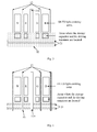
- FIG. 1 four pixel units arranged in order are shown in FIG. 1 , and light emitted from the areas corresponding to the OLED light-emitting units included in the four pixel units arranged in order is of different colors, which are indicated by R, G, B and W in FIG. 1 , indicating the color of red, green, blue and white respectively.
- the colors of the light emitted from the areas that the light-emitting units are located include but are not limited to those in the embodiment illustrated by FIG. 1 .
- the wire mentioned above comprises a gate line 21
- the conductive layer mentioned above comprises a second common power supply line 92 parallel with the gate line 21
- the second common power supply line 92 is overlapped with the gate line 21 in the direction perpendicular to the OLED array substrate (the gate line 21 at a lower position is indicated by the dashed line).
- the second common power supply line 92 is located right above the gate line 21 .
- the conductive layer is disposed on the insulation layer and is far away from the gate line, the risk of electro-static discharge (ESD) between the gate line and the conductive layer is reduced.
- ESD electro-static discharge
- the second common power supply line 92 can be set wider in order to be overlapped with the area that the driving transistor and the storage capacitor are located in the direction perpendicular to the OLED array substrate. In this way, a transverse big covering area of the conductive layer is formed in the area where the gate line 21 , the driving transistor and the storage capacitor are located, which makes the second common power supply line 92 have a greater width and reduces the resistance voltage drop (IR drop) of the conductive layer and the power consumption of the OLED array substrate.
- IR drop resistance voltage drop
- the wire mentioned above comprises a data line 52
- the conductive layer mentioned above comprises a third common power supply line 93 parallel with the data line 52
- the third common power supply line 93 is overlapped with the data line 52 in the direction perpendicular to the OLED array substrate (the data line 52 at a lower position is indicated by the dashed line).
- the third common power supply line 93 is located right above the data line 52 .
- FIG. 1 to FIG. 4 only show the case that a conductive layer comprises one of the first common power supply line 91 , the second common power supply line 92 , and the third common power supply line 93 respectively, which is not limited to the embodiments of the present disclosure.
- the conductive layer mentioned above may comprise both the first common power supply line and the second common power supply line mentioned above, and the first common power supply line and the second common power supply line can be connected with each other to form an integrated structure; or as illustrated in FIG.
- the conductive layer mentioned above may comprise all the first common power supply line, the second common power supply line and the third common power supply line mentioned above, and the first common power supply line, the second common power supply line and the third common power supply line can be connected with one another to form an integrated structure, so that the area of the conductive layer can be larger and the resistance voltage drop (IR drop) of the conductive layer can be smaller.
- IR drop resistance voltage drop
- the OLED array substrate further comprises a data line reserved pattern 53 which is disposed in the same layer as the data line.
- the data line reserved pattern 53 is connected with the source electrode 50 of the driving transistor T 3 (e.g., a driving TFT) (e.g., the two are formed in an integrated structure), and is connected with a data line lead 22 (for example, the data line lead 22 is disposed in the same layer as the gate electrode 20 of the driving transistor T 3 ) through a via hole running through the insulator layer 30 .
- the data line is configured to transmit data voltage signals for the OLED light-emitting unit
- the data line reserved pattern 53 is configured to transfer and to connect the data line and the data line lead 22
- the data line lead 22 is configured to connect a source driver (e.g., a source drive IC) and the data line reserved pattern 53 so as to connect the source driver and the data line.
- the conductive layer 90 is connected with the source electrode 50 of the driving transistor T 3 and the data line reserved pattern 53 through a first via hole (indicated as “a” in the drawings) and a second via hole (indicated as “b” in the drawings) running through the insulation layer 60 respectively.
- the data line reserved pattern 53 mentioned above is usually located in a periphery which is outside the display area (indicated as AA area, meaning an Active Area).
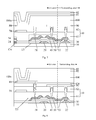
- the stacked structures in FIG. 7 are as follows in order: the substrate 10 ⁇ the gate electrode 20 of the driving transistor T 3 , the gate line, and the data line lead 22 which is disposed in the same layer as the gate electrode ⁇ the gate insulation layer 30 ⁇ the active layer 40 of the driving transistor T 3 ⁇ the source electrode 50 and the drain electrode 51 of the driving transistor T 3 , the data line, and the data line reserved pattern 53 which is disposed in the same layer as the data line ⁇ the protective layer 61 ⁇ the color filter layer 70 ⁇ the planarization layer 62 ⁇ the first electrode 80 of the light-emitting unit and the conductive layer 90 (for example, the first electrode 80 and the conductive layer 90 are disposed side-by-side on the planarization layer 62 ) ⁇ the pixel-defining layer 100 ⁇ the light-emitting layer 81 of the OLED light-emitting unit ⁇ the second electrode 82 of the OLED light-emitting unit.
- At least one of the gate electrode 20 , the active layer 40 , the source electrode 50 and the drain electrode 51 of the driving transistor T 3 comprises a portion that is not overlapped with the block first electrode 80 of the OLED light-emitting unit in the direction perpendicular to the substrate 10 .
- the insulation layer 60 mentioned above may comprise the protective layer 61 (usually called as PSA layer for short) covering the driving transistor T 3 and the planarization layer 62 (usually called for short as OC layer, i.e., Overcoat layer) on the protective layer 61 and covering the color filter 70 , and for example the insulation layer 60 consists of these two layers, so that the first via hole and the second via hole mentioned above both run through these two layers.
- the protective layer 61 usually called as PSA layer for short
- the planarization layer 62 usually called for short as OC layer, i.e., Overcoat layer
- the OLED array substrate further comprises an insulation interlayer 120 which covers the conductive layer 90 and the insulation layer 60 , and the first electrode 80 of the OLED light-emitting unit is disposed on the insulation interlayer 120 .
- the insulation interlayer 120 mentioned above is further disposed between the conductive layer and the insulation layer in the embodiment of the present disclosure in order to guarantee that a short circuit will not occur between the first electrode 80 (i.e., the pixel electrode which can be made of ITO for example) of the OLED light-emitting unit and the conductive layer 90 .
- the distance between the conductive layer 90 and the first electrode 80 can be shorten to increase the aperture ratio to a further degree, so that the resistance voltage drop of the conductive layer can be reduced and the aperture ratio can also be increased to a further degree.
- the drain electrode d 3 of the driving transistor T 3 is electrically connected with the anode (an example of the first electrode 80 ) of the OLED light-emitting unit and a source electrode s 2 of the second transistor T 2 ; one end of the storage capacitor Cst is electrically connected with the drain electrode of the first transistor T 1 and the other end of the storage capacitor Cst is electrically connected with the drain electrode g 3 of the driving transistor T 3 ; the cathode (an example of the second electrode 82 ) of the OLED light-emitting unit is grounded; a gate electrode g 2 of the second transistor T 2 is electrically connected with the detection and compensation line G 2 .
- Vth threshold voltage
- the top electrode 54 of the storage capacitor Cst can be, for example, disposed in the same layer as the source electrode 50 and the drain electrode 51 of the driving transistor T 3
- the bottom electrode 24 of the storage capacitor Cst can be disposed in the same layer as the gate electrode 20 of the driving transistor T 3 .
- the step of forming the first electrode and the conductive layer on the insulation layer comprises: forming on the insulation layer the conductive layer comprising the third common power supply line which is approximately parallel with the data line and is overlapped with the data line in the direction perpendicular to the OLED array substrate; as illustrated in FIG. 8 , forming the insulation interlayer 120 covering the conductive layer 90 and the fourth via hole (indicated as d in the drawing) in the insulation interlayer 120 and communicated with the third via hole (indicated as c in the drawing); forming on the insulation interlayer 120 the first electrode 80 , which is connected with the drain electrode 51 of the driving transistor T 3 through the third via hole c and the fourth via hole d.
- the insulation interlayer mentioned above is further disposed between the conductive layer and the insulation layer in the embodiment of the present disclosure in order to guarantee that a short circuit will not occur between the first electrode (i.e., the pixel electrode which can be made of ITO for example) of the OLED light-emitting unit and the conductive layer.
- the distance between the conductive layer 90 and the first electrode 80 can be shorten to further increase the aperture ratio, so that the resistance voltage drop of the conductive layer can be reduced and the aperture ratio can also be increased to a further degree.
- the method mentioned above are illustrated in FIG. 11( a ) for example, comprising: forming in order on the substrate the gate metal layer comprising the gate electrode, the gate line, the data line lead which is disposed in the same layer as the gate electrode ⁇ the gate insulation layer ⁇ the active layer ⁇ the etch stop layer (here, the step of forming the etch stop layer can be omitted when the material of the active layer is not susceptible to etching for the source-drain electrode, details can be referred to the art of state and is not limited to embodiments of the present disclosure) ⁇ the source-drain metal layer comprising the source electrode, the drain electrode, the data line and the data line reserved pattern which is disposed in the same layer as the data line ⁇ the protective layer ⁇ the color filter layer ⁇ the planarization layer ⁇ the conductive layer ⁇ the insulation interlayer—the first electrode of the OLED light-emitting unit ⁇ the pixel-defining layer ⁇ the light-emitting layer of the OLED
- the gate metal layer, the active layer, the etch stop layer, the source-drain metal layer, the protective layer, the color filter layer, the planarization layer, the metal conductive layer, the insulation interlayer, the first electrode and the pixel-defining layer can all be formed with a patterning process.
- At least one embodiment of the present disclosure further provides another array substrate, and as illustrated in FIG. 12 , the array substrate comprises a plurality of pixel units and each pixel unit comprises a light-emitting unit (indicated with R, G, B, W in FIG.
- a driving transistor T 3 and a storage capacitor Cst which are connected with the light-emitting unit; and a wire LW (indicated by the dashed line), which is connected with the pixel unit P (for example, connected with the driving transistors of the pixel unit); an insulation layer IL, which covers the driving transistor T 3 , the storage capacitor Cst and the wire LW; and a conductive layer CL, which is on the insulation layer IL and is configured to provide a common voltage to the pixel unit.
- the conductive layer CL comprises a portion which is overlapped with at least one of the wire LW, the driving transistor T 3 and the storage capacitor Cst in the direction perpendicular to the array substrate. That the conductive layer CL is overlapped with the wire LW is illustrated in FIG. 12 for example.
- the array substrate comprises a display area (the structure as illustrated in FIG. 12 is located in the display area of the array substrate) and a surrounding area located in a periphery of the display area (not shown in FIG. 12 ).
- the display area comprises a plurality of light-emitting areas (areas indicated by R, G, B and W) corresponding to a plurality of OLED light-emitting units of the plurality of pixel units and a non-light-emitting area located in an area other than the plurality of light-emitting areas.
- the overlapping potion of the conductive layer is located in the non-light-emitting area.
- the wire LW can be a gate line, a data line or a detection and compensation line.
- the wire LW when the wire LW is a gate line, the wire LW can be connected with the gate electrode of the driving transistor T 3 ; when the wire LW is a data line, the wire LW can be connected with the source electrode or the drain electrode of the driving transistor T 3 ; when the wire LW is a detection and compensation line, the wire LW can be connected with the drain electrode of the driving transistor T 3 by way of another transistor (see the embodiment as illustrated in FIG. 9 ).
- the light-emitting unit can be OLED (organic light-emitting diode), LED (light-emitting diode), or other types of active light-emitting devices.
- the array substrate can be an OLED array substrate, or an LED array substrate or other types of active light-emitting array substrates.
- an embodiment of the present disclosure further provide a display device comprising any one of the OLED array substrates or array substrates.
- the display device mentioned above can be an OLED display device, an OLED television, a digital photo frame, a mobile phone, a tablet computer or a product or a component which possesses any display function.
Landscapes
- Engineering & Computer Science (AREA)
- Microelectronics & Electronic Packaging (AREA)
- Physics & Mathematics (AREA)
- Geometry (AREA)
- Computer Hardware Design (AREA)
- General Physics & Mathematics (AREA)
- Theoretical Computer Science (AREA)
- Optics & Photonics (AREA)
- Electroluminescent Light Sources (AREA)
- Devices For Indicating Variable Information By Combining Individual Elements (AREA)
Abstract
Description
- Embodiments of the present disclosure relate to an organic light-emitting diode (OLED) array substrate and a manufacturing method thereof, an array substrate and a display device.
- Nowadays, one mainstream display mode of organic light-emitting diode display (OLED) device is oxide TFT (oxide thin film transistor) plus WOLED (white OLED) plus COA (color filter on array, i.e., the color filter film is formed on the array substrate). In order to solve the problem of threshold voltage (Vth) drift and luminance nonuniformity, a 3T1C external compensation technology is usually applied in the above mainstream display mode for driving pixels, and here the phrase “3T1C” means a pixel unit comprises three thin film transistors (TFT) and one storage capacitor Cst.
- Embodiments of the present disclosure provide an OLED array substrate and a manufacturing method thereof, an array substrate and a display device. Embodiments of the present disclosure can reduce the effective display area occupied by the common power supply lines on the OLED array substrate.
- In one aspect, an embodiment of the present disclosure provides an OLED array substrate, and the OLED array substrate comprises a plurality of pixel units, each of which comprises an OLED light-emitting unit, a driving transistor and a storage capacitor; a wire; an insulation layer which covers the driving transistor, the storage capacitor and the wire; a conductive layer which is on the insulation layer and is configured to provide the common voltage to the pixel unit. At least one of the wire, the driving transistor and the storage capacitor is overlapped with the conductive layer in a direction perpendicular to the OLED array substrate.
- For example, the wire comprises a detection and compensation line which is configured to connect the plurality of pixel units and a detection integrated circuit; and the conductive layer comprises a first common power supply line which is overlapped with the detection and compensation line in the direction perpendicular to the OLED array substrate.
- For example, the wire comprises a gate line, and the conductive layer comprises a second common power supply line which is parallel with the gate line and is overlapped with the gate line in the direction perpendicular to the OLED array substrate.
- For example, the second common power supply line is overlapped with an area that the driving transistor is located and an area that the storage capacitor is located in the direction perpendicular to the OLED array substrate.
- For example, the wire comprises a data line; and the conductive line comprises a third common power supply line which is overlapped with the data line in the direction perpendicular to the OLED array substrate.
- For example, the wire comprises a data line; the OLED array substrate further comprises a data line reserved pattern; and the conductive layer is connected to a source electrode of the driving transistor and the data line reserved pattern respectively through a first via hole and a second via hole which run through the insulation layer.
- For example, the OLED array substrate further comprises a base substrate, and the OLED light-emitting unit comprises a first electrode, a light-emitting layer and a second electrode which are away from the substrate in base sequence; the OLED array substrate further comprises an insulation interlayer covering the conductive layer and the insulation layer in a case where the conductive layer comprises a third common power supply line; and the first electrode is disposed on the insulation interlayer.
- For example, each of the plurality of pixel units further comprises a first transistor and a second transistor, and the OLED array substrate comprises a plurality of wires comprising a data line, a gate line and a detection and compensation line; a source electrode of the first transistor is electrically connected with the data line, a drain electrode of the first transistor is electrically connected with a gate electrode of the driving transistor, and a gate electrode of the first transistor is electrically connected with gate line; a source electrode of the driving transistor is electrically connected with the conductive layer, a drain electrode of the first transistor is electrically connected with an anode of the OLED light-emitting unit and a source electrode of the second transistor; one end of the storage capacitor is electrically connected with the drain electrode of the first transistor, and the other end of the storage capacitor is electrically connected with a drain electrode of the driving transistor; a cathode of the OLED light-emitting unit is grounded; a gate electrode of the second transistor is electrically connected with the detection and compensation line.
- For example, the wire is a metal wire and/or the conductive layer is a metal conductive layer.
- For example, the OLED array substrate comprises a display area and a surrounding area located in a periphery of the display area; the display area comprises a plurality of light-emitting areas corresponding to a plurality of OLED light-emitting units of the plurality of pixel units and a non-light-emitting area located in an area other than the plurality of light-emitting areas; and a portion of the conductive layer is at least partially located outside the plurality of light-emitting areas, which portion of the conductive layer is overlapped with at least one of the wire, the driving transistor and the storage capacitor.
- In another aspect, an embodiment of the present disclosure provides manufacturing method of an OLED array substrate and the method comprises: forming a wire; forming a pixel unit, wherein the pixel unit comprises an OLED light-emitting unit, a driving transistor and a storage capacitor; forming an insulation layer which covers the pixel unit and the wire; and forming a conductive layer which is on the insulation layer and is overlapped with at least one of the wire, and the driving transistor and the storage capacitor is overlapped with the conductive layer in a direction perpendicular to the OLED array substrate, and the conductive layer is configured to provide a common voltage to the pixel unit.
- For example, the wire formed comprises a data line; a data line reserved pattern is formed in a same layer as the data line; the insulation layer is formed cover the driving transistor, the storage capacitor and the wire; the conductive layer is connected with a source electrode of the driving transistor and the data line reserved pattern through a first via hole and a second via hole respectively, and the first via hole and the second via hole run through the insulation layer; a third via hole which exposes a drain electrode of the driving transistor is formed in the insulation layer; a first electrode and the conductive layer are formed on the insulation layer and the first electrode is connected with the drain electrode of the driving transistor through the third via hole; a pixel-defining layer is formed which covers the first electrode and the conductive layer; a light-emitting layer is formed in an opening of the pixel-defining layer; and a second electrode is formed on the light-emitting layer; wherein the OLED light-emitting unit comprises the first electrode, the light-emitting layer and the second electrode.
- For example, forming the first electrode and the conductive layer on the insulation layer comprises: forming the conductive layer on the insulation layer, wherein the conductive layer formed comprises a third common power supply line parallel with the data line, and the third common power supply line is overlapped with the data line in the direction perpendicular to the OLED array substrate; forming the insulation interlayer covering the conductive layer and a fourth via hole which is communicated with the third via hole is formed in the insulation interlayer; and forming the first electrode on the insulation interlayer, wherein the first electrode is connected with the drain electrode of the driving transistor through the third via hole and the fourth via hole.
- For example, the wire is a metal wire and/or the conductive layer is a metal conductive layer.
- In still another aspect, an embodiment of the present disclosure further provides an array substrate comprising a plurality of pixel units, and each of the plurality of pixel units comprises a light-emitting unit, and a driving transistor and a storage capacitor which are connected with the light-emitting unit; a wire, which is connected with the plurality of pixel units; an insulation layer, which covers the driving transistor, the storage capacitor and the wire; and a conductive layer, which is on the insulation layer and is configured to provide a common voltage for the pixel unit; wherein the conductive layer comprises a portion which is overlapped with at least one of the wire, the driving transistor and the storage capacitor in a direction perpendicular to the OLED array substrate.
- For example, the array substrate comprises a display area and a surrounding area located in a periphery of the display area, and the display area comprises a plurality of light-emitting areas corresponding to a plurality of light-emitting units of the plurality of pixel units and a non-light-emitting area located in an area other than the plurality of light-emitting areas, and the portion of the conductive layer is located outside the non-light-emitting area.
- In further still another aspect, an embodiment of the present disclosure further provides an array substrate comprising any one of the OLED array substrates mentioned above or any one of the array substrates mentioned above.
- In order to clearly illustrate the technical solution of the embodiments of the disclosure, the drawings of the embodiments will be briefly described in the following; it is obvious that the described drawings are only related to some embodiments of the disclosure and thus are not limitative of the disclosure.
-
FIG. 1 a first schematic plan view of an OLED array substrate provided by an embodiment of the present disclosure; -
FIG. 2 is a second schematic plan view of an OLED array substrate provided by an embodiment of the present disclosure; -
FIG. 3 is a third schematic plan view of an OLED array substrate provided by an embodiment of the present disclosure; -
FIG. 4 is a fourth schematic plan view of an OLED array substrate provided by an embodiment of the present disclosure; -
FIG. 5 is a fifth schematic plan view of an OLED array substrate provided by an embodiment of the present disclosure; -
FIG. 6 is a sixth schematic plan view of an OLED array substrate provided by an embodiment of the present disclosure; -
FIG. 7 is a first cross sectional view of an OLED array substrate provided by an embodiment of the present disclosure; -
FIG. 8 is a second cross sectional view of an OLED array substrate provided by an embodiment of the present disclosure; -
FIG. 9 is a schematic view of an external compensating circuit of a 3T1C driving pixel structure provided by an embodiment of the present disclosure; -
FIG. 10 is a first flowchart of a manufacturing method of an OLED array substrate provided by an embodiment of the present disclosure; -
FIG. 11 is a second flowchart of a manufacturing method of an OLED array substrate provided by an embodiment of the present disclosure; and -
FIG. 12 is a schematic top view of an array substrate provided by an embodiment of the present disclosure. - In order to make objects, technical details and advantages of the embodiments of the disclosure apparent, the technical solutions of the embodiments will be described in a clearly and fully understandable way in connection with the drawings related to the embodiments of the disclosure. Apparently, the described embodiments are just a part but not all of the embodiments of the disclosure. Based on the described embodiments herein, those skilled in the art can obtain other embodiment(s), without any inventive work, which should be within the scope of the disclosure.
- Unless otherwise defined, all the technical and scientific terms used herein have the same meanings as commonly understood by one of ordinary skill in the art to which the present disclosure belongs. The terms “first,” “second,” etc., which are used in the description and the claims of the present application for disclosure, are not intended to indicate any sequence, amount or importance, but distinguish various components. Also, the terms such as “a,” “an,” etc., are not intended to limit the amount, but indicate the existence of at least one. The terms “comprise,” “comprising,” “include,” “including,” etc., are intended to specify that the elements or the objects stated before these terms encompass the elements or the objects and equivalents thereof listed after these terms, but do not preclude the other elements or objects. The phrases “connect”, “connected”, etc., are not intended to define a physical connection or mechanical connection, but may include an electrical connection, directly or indirectly. “On,” “under,” “right,” “left” and the like are only used to indicate relative position relationship, and when the position of the object which is described is changed, the relative position relationship may be changed accordingly.
- During the research, the inventors of the present disclosure noticed the pixel aperture ratio of an OLED display device is relatively small when the 3T1C external compensation technology is applied to drive the pixels in the OLED display device; and due to the reduced pixel aperture ratio, the luminous intensity of the OLED display device must be increased in order to make up for the affect caused by the reduced pixel aperture ratio upon the display of the OLED display device, and the lifetime of the OLED display device is affected as a result.
- Because the sizes of the patterns in the OLED array substrate involved in the embodiments of the present disclosure are very small, the sizes of the structure patterns in the drawings of the embodiments of the present disclosure are all enlarged for the purpose of clarity. Unless otherwise specified, the drawings are not drawn in a real size or a real scale.
- It should be noted that in the description of the embodiments of the present disclosure, the phrase “A is overlapped with B in a direction perpendicular to the OLED array substrate” means that A is completely overlapped with B in a direction perpendicular to the OLED array substrate, or A is partially overlapped with B in the direction perpendicular to the OLED array substrate. In addition, the direction perpendicular to the OLED array substrate means the direction perpendicular to the bearing surface of the bearing substrate included in the array substrate. It is not limited in the embodiments of the present disclosure. The former can be chosen in order to increase pixel aperture ratio better.
- An embodiment of the present disclosure provides an OLED array substrate, and the OLED array substrate comprises a plurality of pixel units. Each pixel unit comprises: an OLED light-emitting unit; a driving transistor (e.g., a driving thin film transistor (TFT)) and a storage capacitor which are connected with the OLED light-emitting unit; and a wire, such as a metal wire, which is connected with the pixel units, for example, the driving transistors of the pixel units; an insulation layer, which covers the driving transistor, the storage capacitor and the wire; and a conductive layer (e.g., a metal conductive layer), which is provided on the insulation layer and is configured to provide a common voltage (VDD) to the pixel units. In the OLED array substrate, at least one of the wire, the driving transistor and the storage capacitor is overlapped with the conductive layer in the direction perpendicular to the OLED array substrate. For example, in the case where the conductive layer is overlapped with the wire, the extending direction of the portion of the conductive layer that is overlapped with the wire is approximately the same as the extending direction of the wire.
- For example, the wire and/or the conductive layer can be made of a metal material, as well as a metal oxide conductive material for example, or other conductive material.
- For example, the driving transistor comprises a gate electrode, an active layer, a source electrode and a drain electrode. In the case where the conductive layer is overlapped with the driving transistor, the conductive layer can be overlapped with at least one of the gate electrode, the active layer, the source electrode and the drain electrode.
- It should be noted that the wire that is mentioned above can be, for example, at least one of a gate line, a data line, and a detection and compensation line (i.e., sense line indicated by SL in
FIG. 9 ) which connects a pixel unit and a detection integrated circuit (i.e., Sense IC, the detecting IC inFIG. 9 ). For example, when the wire is a gate line, the wire can be connected with the gate electrode of the driving transistor T3; when the wire is a data line, the wire can be connected with the source electrode or the drain electrode of the driving transistor T3; when the wire is a detection and compensation line, the wire can be connected with the drain electrode of the driving transistor T3 through another transistor (see the embodiment shown inFIG. 9 ). - In addition, for those skilled in the art, the above mentioned OLED array substrate comprises a display area and a surrounding area located outside the display area; the display area is also referred to as AA (Active Area) area and generally used for performing display. The display area comprises a plurality of light-emitting areas corresponding to the plurality of OLED light-emitting units of the plurality of pixel units and a non-light-emitting area located in a periphery of the plurality of light-emitting areas; and the portion of the conductive layer is at least partially located outside the plurality of light-emitting areas, which portion of the conductive layer is overlapped with at least one of the wire, the driving transistor and the storage capacitor. The surrounding area can be configured for disposing a driving circuit and the like therein. The plurality of pixel units and the wire mentioned above are all disposed in the display area.
- In this way, because the conductive layer configured for providing a common voltage VDD to the plurality of pixel units is disposed above the insulation layer, and is overlapped with at least one of the wire that is lightproof, the driving transistor that is lightproof and the storage capacitor that is lightproof in the direction perpendicular to the OLED array substrate, the portion of the effective display area (the light-emitting areas that all the OLED light-emitting units of the plurality of the pixel units in the display area are located) occupied by the conductive layer acting as the common power supply line on the OLED array substrate is reduced, and therefore the aperture ratio of the display device comprising the OLED array substrate is increased. Because the aperture ratio is increased, there is no need to increase the luminous intensity of the OLED display device in order to make up for the affect caused by the reduced pixel aperture ratio upon the display of the OLED display device, and the lifetime of the OLED device of an OLED display panel is increased as a result.
- For example, the conductive mentioned above can be a common power supply line. The OLED substrates provided by embodiments of the present disclosure are specified as follows according to different positions of the conductive layer and different situations for the wire.
- Based on any one of the embodiment mentioned above, for example, as illustrated in
FIG. 1 , the wire mentioned above comprises a detection andcompensation line 110 which connects a pixel unit and a detection integrated circuit. For example, as illustrated inFIG. 9 , a detection and compensation line SL can be connected with a pixel unit and a detection integrated circuit; the conductive layer mentioned above comprises a first commonpower supply line 91 which is approximately parallel with the detection andcompensation line 110, and the first commonpower supply line 91 is overlapped with the detection andcompensation line 110 in the direction perpendicular to the OLED array substrate (the detection andcompensation line 110 at a lower position is indicated by the dashed line). For example, the first commonpower supply line 91 is located right above the detection andcompensation line 110. - Because the detection and compensation line is overlapped with the first common power supply line in the direction perpendicular to the OLED array substrate, a capacitor is generated between the detection and compensation line and the first common power supply line, which increases the capacitance between the detection and compensation line and other conductive structure overlapped with the detection and compensation line and guarantees the stability of the capacitance.
- For example, as illustrated in
FIG. 1 , the extending direction of the detection andcompensation line 110 is approximately parallel with the extending direction of adata line 52; for example, the width of the detection andcompensation line 110 is greater than the width of thedata line 52. - It should be noted that four pixel units arranged in order are shown in
FIG. 1 , and light emitted from the areas corresponding to the OLED light-emitting units included in the four pixel units arranged in order is of different colors, which are indicated by R, G, B and W inFIG. 1 , indicating the color of red, green, blue and white respectively. The colors of the light emitted from the areas that the light-emitting units are located include but are not limited to those in the embodiment illustrated byFIG. 1 . - Based on any one of the embodiment mentioned above, for example, as illustrated in
FIG. 2 , the wire mentioned above comprises agate line 21, the conductive layer mentioned above comprises a second commonpower supply line 92 parallel with thegate line 21, and the second commonpower supply line 92 is overlapped with thegate line 21 in the direction perpendicular to the OLED array substrate (thegate line 21 at a lower position is indicated by the dashed line). For example, the second commonpower supply line 92 is located right above thegate line 21. - In this embodiment, because the conductive layer is disposed on the insulation layer and is far away from the gate line, the risk of electro-static discharge (ESD) between the gate line and the conductive layer is reduced.
- For example, by considering that the area that the gate line is located is close to the area that the driving transistor and the storage capacitor are located, as illustrated in
FIG. 3 , the second commonpower supply line 92 can be set wider in order to be overlapped with the area that the driving transistor and the storage capacitor are located in the direction perpendicular to the OLED array substrate. In this way, a transverse big covering area of the conductive layer is formed in the area where thegate line 21, the driving transistor and the storage capacitor are located, which makes the second commonpower supply line 92 have a greater width and reduces the resistance voltage drop (IR drop) of the conductive layer and the power consumption of the OLED array substrate. - Based on any one of the embodiment mentioned above, for example, as illustrated in
FIG. 4 , the wire mentioned above comprises adata line 52, the conductive layer mentioned above comprises a third commonpower supply line 93 parallel with thedata line 52, and the third commonpower supply line 93 is overlapped with thedata line 52 in the direction perpendicular to the OLED array substrate (thedata line 52 at a lower position is indicated by the dashed line). For example, the third commonpower supply line 93 is located right above thedata line 52. - It should be noted that
FIG. 1 toFIG. 4 only show the case that a conductive layer comprises one of the first commonpower supply line 91, the second commonpower supply line 92, and the third commonpower supply line 93 respectively, which is not limited to the embodiments of the present disclosure. For example, as illustrated inFIG. 5 , the conductive layer mentioned above may comprise both the first common power supply line and the second common power supply line mentioned above, and the first common power supply line and the second common power supply line can be connected with each other to form an integrated structure; or as illustrated inFIG. 6 , the conductive layer mentioned above may comprise all the first common power supply line, the second common power supply line and the third common power supply line mentioned above, and the first common power supply line, the second common power supply line and the third common power supply line can be connected with one another to form an integrated structure, so that the area of the conductive layer can be larger and the resistance voltage drop (IR drop) of the conductive layer can be smaller. - For example, as illustrated in
FIG. 7 , the OLED array substrate further comprises a data line reservedpattern 53 which is disposed in the same layer as the data line. For example, the data line reservedpattern 53 is connected with thesource electrode 50 of the driving transistor T3 (e.g., a driving TFT) (e.g., the two are formed in an integrated structure), and is connected with a data line lead 22 (for example, thedata line lead 22 is disposed in the same layer as thegate electrode 20 of the driving transistor T3) through a via hole running through theinsulator layer 30. The data line is configured to transmit data voltage signals for the OLED light-emitting unit, the data line reservedpattern 53 is configured to transfer and to connect the data line and thedata line lead 22, and thedata line lead 22 is configured to connect a source driver (e.g., a source drive IC) and the data line reservedpattern 53 so as to connect the source driver and the data line. Theconductive layer 90 is connected with thesource electrode 50 of the driving transistor T3 and the data line reservedpattern 53 through a first via hole (indicated as “a” in the drawings) and a second via hole (indicated as “b” in the drawings) running through theinsulation layer 60 respectively. The data line reservedpattern 53 mentioned above is usually located in a periphery which is outside the display area (indicated as AA area, meaning an Active Area). - It should be noted that the stacked structures in
FIG. 7 are as follows in order: thesubstrate 10→thegate electrode 20 of the driving transistor T3, the gate line, and thedata line lead 22 which is disposed in the same layer as the gate electrode→thegate insulation layer 30→theactive layer 40 of the driving transistor T3→thesource electrode 50 and thedrain electrode 51 of the driving transistor T3, the data line, and the data line reservedpattern 53 which is disposed in the same layer as the data line→theprotective layer 61→thecolor filter layer 70→theplanarization layer 62→thefirst electrode 80 of the light-emitting unit and the conductive layer 90 (for example, thefirst electrode 80 and theconductive layer 90 are disposed side-by-side on the planarization layer 62)→the pixel-defininglayer 100→the light-emittinglayer 81 of the OLED light-emitting unit→thesecond electrode 82 of the OLED light-emitting unit. - For example, at least one of the
gate electrode 20, theactive layer 40, thesource electrode 50 and thedrain electrode 51 of the driving transistor T3 comprises a portion that is not overlapped with the blockfirst electrode 80 of the OLED light-emitting unit in the direction perpendicular to thesubstrate 10. - For example, the OLED array substrate comprises the pixel-defining
layer 100 and theopening 100 a of the pixel-defininglayer 100 exposes at least a portion of the surface of thefirst electrode 80 of the OLED light-emitting unit. Each of the light-emittinglayer 81 and thesecond electrode 82 of the OLED light-emitting unit comprises a portion which is in theopening 100 a. - For example, the
top electrode 54 of the storage capacitor Cst can be, for example, disposed in the same layer as thesource electrode 50 and thedrain electrode 51 of the driving transistor T3, and thebottom electrode 24 of the storage capacitor Cst can be disposed in the same layer as thegate electrode 20 of the driving transistor T3. For example, each of thetop electrode 54 and thebottom electrode 24 of the storage capacitor Cst comprises a portion which is not overlapped with thefirst electrode 80 of the OLED light-emitting unit in the direction perpendicular to thesubstrate 10. - In the embodiment, because the current mainstream OLED array substrates are COA substrates which are integrated with color filters, therefore the stacked structures as illustrated in
FIG. 7 may further comprise acolor filter 70. For example, thecolor filter 70 is overlapped with thefirst electrode 80 of the OLED light-emitting unit in the direction perpendicular to thesubstrate 10. In this case, theinsulation layer 60 mentioned above may comprise the protective layer 61 (usually called as PSA layer for short) covering the driving transistor T3 and the planarization layer 62 (usually called for short as OC layer, i.e., Overcoat layer) on theprotective layer 61 and covering thecolor filter 70, and for example theinsulation layer 60 consists of these two layers, so that the first via hole and the second via hole mentioned above both run through these two layers. - For example, in a case that the conductive layer mentioned above comprises a third common power supply line, as illustrated in
FIG. 8 , the OLED array substrate further comprises aninsulation interlayer 120 which covers theconductive layer 90 and theinsulation layer 60, and thefirst electrode 80 of the OLED light-emitting unit is disposed on theinsulation interlayer 120. - In the embodiment, because the third common power supply line is disposed above the data line and is overlapped with the data line, the
insulation interlayer 120 mentioned above is further disposed between the conductive layer and the insulation layer in the embodiment of the present disclosure in order to guarantee that a short circuit will not occur between the first electrode 80 (i.e., the pixel electrode which can be made of ITO for example) of the OLED light-emitting unit and theconductive layer 90. In this way, the distance between theconductive layer 90 and thefirst electrode 80 can be shorten to increase the aperture ratio to a further degree, so that the resistance voltage drop of the conductive layer can be reduced and the aperture ratio can also be increased to a further degree. - For example, as can be seen from
FIG. 9 , the pixel unit further comprises a first transistor T1 and a second transistor T2; the wire comprises a data line Da, a gate line G1 and a detection and compensation line G2; a source electrode s1 of the first transistor T1 is electrically connected with the data line Da, a drain electrode d1 of the first transistor T1 is electrically connected with the gate electrode g3 of the driving transistor T3, a gate electrode g1 of the first transistor T1 is electrically connected with the gate line G1; the source electrode s3 of the driving transistor T3 is electrically connected with the conductive layer (see VDD inFIG. 9 ), and the drain electrode d3 of the driving transistor T3 is electrically connected with the anode (an example of the first electrode 80) of the OLED light-emitting unit and a source electrode s2 of the second transistor T2; one end of the storage capacitor Cst is electrically connected with the drain electrode of the first transistor T1 and the other end of the storage capacitor Cst is electrically connected with the drain electrode g3 of the driving transistor T3; the cathode (an example of the second electrode 82) of the OLED light-emitting unit is grounded; a gate electrode g2 of the second transistor T2 is electrically connected with the detection and compensation line G2. In this way, a 3T1C external compensation configuration is obtained, which can solve the problem of threshold voltage (Vth) drift and luminance nonuniformity of the oxide TFT. - For example, an embodiment of the present disclosure further comprises a manufacturing method of the OLED array substrate mentioned above and the method comprises steps of: forming a wire and a plurality of pixel units, wherein the formed pixel unit comprises an OLED light-emitting unit, a driving transistor and a storage capacitor; forming an insulation layer which covers the pixel unit and the wire. The method mentioned above further comprises: forming a conductive layer which is on the insulation layer and is overlapped with at least one of the wire, the driving transistor and the storage capacitor in the direction perpendicular to the OLED array substrate, and the conductive layer is configured to provide a common voltage to the pixel unit.
- For example, the wire is a metal wire and/or the conductive layer is a metal conductive layer.
- Taking the OLED array substrate as illustrated in
FIG. 8 as an example, for example, the method mentioned above comprises: forming the driving transistor T3, the storage capacitor, and the wire on the base substrate 10, the formed wire including the data line; forming the data line reserved pattern 53 which is disposed in the same layer as the data line; forming the insulation layer 60 which covers the driving transistor T3, the storage capacitor and the wire, and forming the third via hole c which exposes the drain electrode 51 of the driving transistor T3 in the insulation layer 60; forming the first electrode 80 and the conductive layer 90 which is configured to provide a common voltage to the pixel unit on the insulation layer 60, allowing the conductive layer 90 to be overlapped with at least one of the wire, the driving transistor T3, and the storage capacitor in the direction perpendicular to the OLED array substrate and connected with the source electrode 50 of the driving transistor T3 and the data line reserved pattern 53 respectively through the first via hole a and the second via hole b that run through the insulation layer 60, and allowing the first electrode 80 to be connected with the drain electrode 51 of the driving transistor T3 through the third via hole c; forming the pixel-defining layer 100 which covers the first electrode 80 and the conductive layer 90; forming the light-emitting layer 81 in the opening 100 a of the pixel-defining layer 100; and forming the second electrode 82 on the light-emitting layer 81. In the embodiment, thefirst electrode 80, the light-emittinglayer 81 and thesecond electrode 82 form the OLED light-emitting unit, and the OLED light-emitting unit, the driving transistor and the storage capacitor form the pixel unit. - For example, the
top electrode 54 of the storage capacitor Cst can be, for example, disposed in the same layer as thesource electrode 50 and thedrain electrode 51 of the driving transistor T3, and thebottom electrode 24 of the storage capacitor Cst can be disposed in the same layer as thegate electrode 20 of the driving transistor T3. - For example, because the current mainstream OLED array substrates are COA substrates which are integrated with color filters, in this case, the insulation layer 60 mentioned above may comprise the protective layer 61 (usually called as PSA layer for short) covering the driving transistor T3 and the planarization layer 62 (usually called for short as OC layer, i.e., Overcoat layer) which is on the protective layer 61 and covers the color filter 70, and therefore the steps of the method mentioned above are illustrated in
FIG. 10(a) for example, comprising: forming in order on the substrate the gate metal layer comprising the gate electrode, the gate line, the data line lead which is disposed in the same layer as the gate electrode→the gate insulation layer→the active layer→the etch stop layer (here, the step of forming the etch stop layer can be omitted when the material of the active layer is not susceptible to etching for the source-drain electrode, details can be referred to the art of state and is not limited to embodiments of the present disclosure)→the source-drain metal layer comprising the source electrode, the drain electrode, the data line, and the data line reserved pattern which is disposed in the same layer as the data line→the protective layer→the color filter layer→the planarization layer→the first electrode of the OLED light-emitting unit and the conductive layer→the pixel-defining layer→the light-emitting layer of the OLED light-emitting unit→the second electrode of the OLED light-emitting unit. In this stacked structure, for example, as can be seen fromFIG. 10(b) , the gate metal layer, the active layer, the etch stop layer, the source-drain metal layer, the protective layer, the color filter layer, the planarization layer, the first electrode, the metal conductive layer and the pixel-defining layer can all be formed with a patterning process, which may be a photolithography process comprising exposing, developing, etching and the like, or other process that can used to form needed patterns in the related art field. - For example, based on any one of the embodiment mentioned above, the step of forming the first electrode and the conductive layer on the insulation layer comprises: forming on the insulation layer the conductive layer comprising the third common power supply line which is approximately parallel with the data line and is overlapped with the data line in the direction perpendicular to the OLED array substrate; as illustrated in
FIG. 8 , forming theinsulation interlayer 120 covering theconductive layer 90 and the fourth via hole (indicated as d in the drawing) in theinsulation interlayer 120 and communicated with the third via hole (indicated as c in the drawing); forming on theinsulation interlayer 120 thefirst electrode 80, which is connected with thedrain electrode 51 of the driving transistor T3 through the third via hole c and the fourth via hole d. - Because the third common power supply line is disposed on the data line and is overlapped with the data line, the insulation interlayer mentioned above is further disposed between the conductive layer and the insulation layer in the embodiment of the present disclosure in order to guarantee that a short circuit will not occur between the first electrode (i.e., the pixel electrode which can be made of ITO for example) of the OLED light-emitting unit and the conductive layer. In this way, the distance between the
conductive layer 90 and thefirst electrode 80 can be shorten to further increase the aperture ratio, so that the resistance voltage drop of the conductive layer can be reduced and the aperture ratio can also be increased to a further degree. - For example, in a case that the operation of forming the
insulation interlayer 120 is comprised, the method mentioned above are illustrated inFIG. 11(a) for example, comprising: forming in order on the substrate the gate metal layer comprising the gate electrode, the gate line, the data line lead which is disposed in the same layer as the gate electrode→the gate insulation layer→the active layer→the etch stop layer (here, the step of forming the etch stop layer can be omitted when the material of the active layer is not susceptible to etching for the source-drain electrode, details can be referred to the art of state and is not limited to embodiments of the present disclosure)→the source-drain metal layer comprising the source electrode, the drain electrode, the data line and the data line reserved pattern which is disposed in the same layer as the data line→the protective layer→the color filter layer→the planarization layer→the conductive layer→the insulation interlayer—the first electrode of the OLED light-emitting unit→the pixel-defining layer→the light-emitting layer of the OLED light-emitting unit→the second electrode of the OLED light-emitting unit. In this stacked structure, for example, as can be seen fromFIG. 11(b) , the gate metal layer, the active layer, the etch stop layer, the source-drain metal layer, the protective layer, the color filter layer, the planarization layer, the metal conductive layer, the insulation interlayer, the first electrode and the pixel-defining layer can all be formed with a patterning process. - At least one embodiment of the present disclosure further provides another array substrate, and as illustrated in
FIG. 12 , the array substrate comprises a plurality of pixel units and each pixel unit comprises a light-emitting unit (indicated with R, G, B, W inFIG. 12 ), a driving transistor T3 and a storage capacitor Cst which are connected with the light-emitting unit; and a wire LW (indicated by the dashed line), which is connected with the pixel unit P (for example, connected with the driving transistors of the pixel unit); an insulation layer IL, which covers the driving transistor T3, the storage capacitor Cst and the wire LW; and a conductive layer CL, which is on the insulation layer IL and is configured to provide a common voltage to the pixel unit. The conductive layer CL comprises a portion which is overlapped with at least one of the wire LW, the driving transistor T3 and the storage capacitor Cst in the direction perpendicular to the array substrate. That the conductive layer CL is overlapped with the wire LW is illustrated inFIG. 12 for example. - For example, the array substrate comprises a display area (the structure as illustrated in
FIG. 12 is located in the display area of the array substrate) and a surrounding area located in a periphery of the display area (not shown inFIG. 12 ). The display area comprises a plurality of light-emitting areas (areas indicated by R, G, B and W) corresponding to a plurality of OLED light-emitting units of the plurality of pixel units and a non-light-emitting area located in an area other than the plurality of light-emitting areas. The overlapping potion of the conductive layer is located in the non-light-emitting area. - For example, the wire LW can be a gate line, a data line or a detection and compensation line. For example, when the wire LW is a gate line, the wire LW can be connected with the gate electrode of the driving transistor T3; when the wire LW is a data line, the wire LW can be connected with the source electrode or the drain electrode of the driving transistor T3; when the wire LW is a detection and compensation line, the wire LW can be connected with the drain electrode of the driving transistor T3 by way of another transistor (see the embodiment as illustrated in
FIG. 9 ). - For example, the light-emitting unit can be OLED (organic light-emitting diode), LED (light-emitting diode), or other types of active light-emitting devices.
- For example, the array substrate can be an OLED array substrate, or an LED array substrate or other types of active light-emitting array substrates.
- Based on any one of the embodiment mentioned above, an embodiment of the present disclosure further provide a display device comprising any one of the OLED array substrates or array substrates.
- For example, the display device mentioned above can be an OLED display device, an OLED television, a digital photo frame, a mobile phone, a tablet computer or a product or a component which possesses any display function.
- The embodiments for the OLED array substrate and the embodiments for the manufacturing method thereof and the embodiments for the display device above can be combined for cross reference.
- In embodiments of the present disclosure, because the conductive layer configured for providing a common voltage VDD to the plurality of pixel units is disposed above the insulation layer, and is overlapped with at least one of the wire that is lightproof, the driving transistor that is lightproof and the storage capacitor that is lightproof in the direction perpendicular to the OLED array substrate, the portion of the effective display area occupied by the conductive layer acting as the common power supply lines on the OLED array substrate is reduced, and therefore the aperture ratio is increased. Because the aperture ratio is increased, there is no need to increase the luminous intensity of the OLED display device in order to make up for the affect caused by the reduced aperture ratio upon the display of the OLED display device, and the lifetime of the OLED device is increased as a result.
- What are described above is related to the illustrative embodiments of the disclosure only and not limitative to the scope of the disclosure; the scopes of the disclosure are defined by the accompanying claims.
- The application claims priority to the Chinese patent application No. 201610371658.2, filed May 30, 2016, the entire disclosure of which is incorporated herein by reference as part of the present application.
Claims (20)
Applications Claiming Priority (4)
| Application Number | Priority Date | Filing Date | Title |
|---|---|---|---|
| CN201610371658 | 2016-05-30 | ||
| CN201610371658.2 | 2016-05-30 | ||
| CN201610371658.2A CN105789266A (en) | 2016-05-30 | 2016-05-30 | OLED array substrate, making method thereof and display device |
| PCT/CN2017/085921 WO2017206796A1 (en) | 2016-05-30 | 2017-05-25 | Oled array substrate, preparation method thereof, array substrate, and display device |
Publications (2)
| Publication Number | Publication Date |
|---|---|
| US20180261663A1 true US20180261663A1 (en) | 2018-09-13 |
| US10453909B2 US10453909B2 (en) | 2019-10-22 |
Family
ID=56375382
Family Applications (1)
| Application Number | Title | Priority Date | Filing Date |
|---|---|---|---|
| US15/570,615 Active US10453909B2 (en) | 2016-05-30 | 2017-05-25 | OLED array substrate with overlapped conductive layer and manufacturing method thereof, array substrate and display device |
Country Status (3)
| Country | Link |
|---|---|
| US (1) | US10453909B2 (en) |
| CN (1) | CN105789266A (en) |
| WO (1) | WO2017206796A1 (en) |
Cited By (15)
| Publication number | Priority date | Publication date | Assignee | Title |
|---|---|---|---|---|
| US10311787B2 (en) * | 2016-12-08 | 2019-06-04 | Boe Technology Group Co., Ltd. | Pixel driving circuit, driving method, pixel unit, and display apparatus |
| US10388714B2 (en) * | 2017-05-27 | 2019-08-20 | Shanghai Tianma AM-OLED Co., Ltd. | Organic light emitting display panel and display terminal |
| CN111384121A (en) * | 2018-12-28 | 2020-07-07 | 乐金显示有限公司 | display device |
| US11127780B2 (en) | 2019-01-28 | 2021-09-21 | Au Optronics Corporation | Display panel |
| CN113646826A (en) * | 2020-02-27 | 2021-11-12 | 京东方科技集团股份有限公司 | Display substrate and preparation method thereof, and compensation method for trace load |
| US20210399022A1 (en) * | 2020-06-22 | 2021-12-23 | Samsung Display Co., Ltd. | Display device |
| WO2022082331A1 (en) * | 2020-10-19 | 2022-04-28 | Boe Technology Group Co., Ltd. | Array substrate and display apparatus |
| KR20220064625A (en) * | 2020-11-12 | 2022-05-19 | 엘지디스플레이 주식회사 | Display panel and display device using the same |
| EP4035209A4 (en) * | 2019-09-27 | 2022-11-09 | BOE Technology Group Co., Ltd. | NETWORK SUBSTRATE, DISPLAY APPARATUS, METHOD FOR MAKING NETWORK SUBSTRATE AND PIXEL DRIVER CIRCUIT |
| US20230038017A1 (en) * | 2019-11-28 | 2023-02-09 | Chengdu Boe Optoelectronics Technology Co.,Ltd. | Display substrate and display device |
| US20230180537A1 (en) * | 2021-12-06 | 2023-06-08 | Samsung Display Co., Ltd. | Light emitting display device |
| GB2614418A (en) * | 2021-12-07 | 2023-07-05 | Lg Display Co Ltd | Light emitting display device and manufacturing method thereof |
| US20240153932A1 (en) * | 2021-05-31 | 2024-05-09 | Chengdu Boe Optoelectronics Technology Co., Ltd. | Array substrate and display panel |
| US12131702B2 (en) * | 2022-07-08 | 2024-10-29 | Samsung Display Co., Ltd. | Display device |
| US12517600B2 (en) * | 2016-08-29 | 2026-01-06 | Semiconductor Energy Laboratory Co., Ltd. | Display device and control program |
Families Citing this family (14)
| Publication number | Priority date | Publication date | Assignee | Title |
|---|---|---|---|---|
| CN105789266A (en) * | 2016-05-30 | 2016-07-20 | 京东方科技集团股份有限公司 | OLED array substrate, making method thereof and display device |
| US10755638B2 (en) * | 2016-08-16 | 2020-08-25 | Apple Inc. | Organic light-emitting diode display with external compensation |
| CN106601778B (en) * | 2016-12-29 | 2019-12-24 | 深圳市华星光电技术有限公司 | OLED backplane and method of making the same |
| US10574249B2 (en) * | 2018-05-02 | 2020-02-25 | Apple Inc. | Capacitor structure with correlated error mitigation and improved systematic mismatch in technologies with multiple patterning |
| CN108899339B (en) * | 2018-05-07 | 2021-04-30 | 武汉天马微电子有限公司 | Display panel and display device |
| JP7256622B2 (en) * | 2018-09-26 | 2023-04-12 | 株式会社ジャパンディスプレイ | Display device |
| KR102678683B1 (en) * | 2018-12-04 | 2024-06-25 | 엘지디스플레이 주식회사 | Electroluminescent Display Device and Display Device |
| EP3723148A1 (en) * | 2019-04-08 | 2020-10-14 | Murata Manufacturing Co., Ltd. | Three-dimensional capacitive structures and their manufacturing methods |
| CN110071120A (en) * | 2019-04-16 | 2019-07-30 | 深圳市华星光电半导体显示技术有限公司 | Display panel and display device |
| EP4068265B1 (en) * | 2019-11-29 | 2025-03-26 | BOE Technology Group Co., Ltd. | Display substrate and manufacturing method therefor, and display device |
| WO2021227062A1 (en) * | 2020-05-15 | 2021-11-18 | 京东方科技集团股份有限公司 | Display panel and electronic apparatus |
| WO2022246808A1 (en) * | 2021-05-28 | 2022-12-01 | 京东方科技集团股份有限公司 | Display device, display panel, and manufacturing method therefor |
| CN113345922B (en) * | 2021-05-28 | 2023-01-24 | 深圳市华星光电半导体显示技术有限公司 | Driving backboard, manufacturing method thereof and display panel |
| KR20230100057A (en) * | 2021-12-28 | 2023-07-05 | 엘지디스플레이 주식회사 | Display device |
Citations (3)
| Publication number | Priority date | Publication date | Assignee | Title |
|---|---|---|---|---|
| US20080017860A1 (en) * | 2006-01-24 | 2008-01-24 | Seiko Epson Corporation | Light-Emitting Device and Electronic Apparatus |
| CN102881711A (en) * | 2012-09-25 | 2013-01-16 | 南京中电熊猫液晶显示科技有限公司 | Active organic light emitting diode (OLED) |
| US20150144904A1 (en) * | 2013-11-25 | 2015-05-28 | Lg Display Co., Ltd. | Organic electroluminescent device and repairing method thereof |
Family Cites Families (15)
| Publication number | Priority date | Publication date | Assignee | Title |
|---|---|---|---|---|
| KR100581903B1 (en) * | 2004-03-09 | 2006-05-22 | 삼성에스디아이 주식회사 | Electroluminescent display device |
| KR100698678B1 (en) | 2004-11-25 | 2007-03-26 | 삼성에스디아이 주식회사 | Light emitting display device and manufacturing method thereof |
| KR100685804B1 (en) | 2004-12-14 | 2007-02-22 | 삼성에스디아이 주식회사 | Organic Electroluminescence Device and Fabricating Method of the same |
| CN100499135C (en) * | 2005-09-29 | 2009-06-10 | 中华映管股份有限公司 | Active element array substrate |
| JP2007148215A (en) | 2005-11-30 | 2007-06-14 | Seiko Epson Corp | LIGHT EMITTING DEVICE AND ELECTRONIC DEVICE |
| US8334545B2 (en) | 2010-03-24 | 2012-12-18 | Universal Display Corporation | OLED display architecture |
| CN102629046B (en) | 2011-06-29 | 2015-05-20 | 北京京东方光电科技有限公司 | Array substrate, manufacturing method of array substrate and liquid crystal display device |
| CN102569348A (en) * | 2012-02-15 | 2012-07-11 | 福州华映视讯有限公司 | Active light-emitting element |
| CN102981336B (en) | 2012-11-29 | 2015-07-15 | 京东方科技集团股份有限公司 | Array substrate, display module and preparation method for array substrate |
| TWI500144B (en) | 2012-12-31 | 2015-09-11 | Lg Display Co Ltd | Organic light emitting display device and method of manufacturing same |
| KR101988217B1 (en) | 2013-01-04 | 2019-06-12 | 엘지디스플레이 주식회사 | Oled micro-cavity structure and method of making |
| KR102082425B1 (en) * | 2013-06-10 | 2020-02-28 | 삼성디스플레이 주식회사 | Flat panel display device |
| CN104133334A (en) * | 2014-08-18 | 2014-11-05 | 信利半导体有限公司 | Pixel structure, array substrate and display device |
| CN105047687B (en) * | 2015-07-03 | 2018-03-27 | 京东方科技集团股份有限公司 | A kind of transparent display panel and display device |
| CN105789266A (en) * | 2016-05-30 | 2016-07-20 | 京东方科技集团股份有限公司 | OLED array substrate, making method thereof and display device |
-
2016
- 2016-05-30 CN CN201610371658.2A patent/CN105789266A/en active Pending
-
2017
- 2017-05-25 WO PCT/CN2017/085921 patent/WO2017206796A1/en not_active Ceased
- 2017-05-25 US US15/570,615 patent/US10453909B2/en active Active
Patent Citations (3)
| Publication number | Priority date | Publication date | Assignee | Title |
|---|---|---|---|---|
| US20080017860A1 (en) * | 2006-01-24 | 2008-01-24 | Seiko Epson Corporation | Light-Emitting Device and Electronic Apparatus |
| CN102881711A (en) * | 2012-09-25 | 2013-01-16 | 南京中电熊猫液晶显示科技有限公司 | Active organic light emitting diode (OLED) |
| US20150144904A1 (en) * | 2013-11-25 | 2015-05-28 | Lg Display Co., Ltd. | Organic electroluminescent device and repairing method thereof |
Cited By (27)
| Publication number | Priority date | Publication date | Assignee | Title |
|---|---|---|---|---|
| US12517600B2 (en) * | 2016-08-29 | 2026-01-06 | Semiconductor Energy Laboratory Co., Ltd. | Display device and control program |
| US10311787B2 (en) * | 2016-12-08 | 2019-06-04 | Boe Technology Group Co., Ltd. | Pixel driving circuit, driving method, pixel unit, and display apparatus |
| US10388714B2 (en) * | 2017-05-27 | 2019-08-20 | Shanghai Tianma AM-OLED Co., Ltd. | Organic light emitting display panel and display terminal |
| CN111384121A (en) * | 2018-12-28 | 2020-07-07 | 乐金显示有限公司 | display device |
| US11127780B2 (en) | 2019-01-28 | 2021-09-21 | Au Optronics Corporation | Display panel |
| EP4035209A4 (en) * | 2019-09-27 | 2022-11-09 | BOE Technology Group Co., Ltd. | NETWORK SUBSTRATE, DISPLAY APPARATUS, METHOD FOR MAKING NETWORK SUBSTRATE AND PIXEL DRIVER CIRCUIT |
| US11721282B2 (en) * | 2019-11-28 | 2023-08-08 | Chengdu Boe Optoelectronics Technology Co., Ltd. | Display substrate and display device |
| US20230038017A1 (en) * | 2019-11-28 | 2023-02-09 | Chengdu Boe Optoelectronics Technology Co.,Ltd. | Display substrate and display device |
| CN113646826A (en) * | 2020-02-27 | 2021-11-12 | 京东方科技集团股份有限公司 | Display substrate and preparation method thereof, and compensation method for trace load |
| KR20210157928A (en) * | 2020-06-22 | 2021-12-30 | 삼성디스플레이 주식회사 | Display device |
| US11830885B2 (en) * | 2020-06-22 | 2023-11-28 | Samsung Display Co., Ltd. | Display device |
| US20210399022A1 (en) * | 2020-06-22 | 2021-12-23 | Samsung Display Co., Ltd. | Display device |
| KR102748572B1 (en) * | 2020-06-22 | 2024-12-31 | 삼성디스플레이 주식회사 | Display device |
| US11974463B2 (en) | 2020-10-19 | 2024-04-30 | Chengdu Boe Optoelectronics Technology Co., Ltd. | Array substrate and display apparatus |
| US12052889B2 (en) | 2020-10-19 | 2024-07-30 | Chengdu Boe Optoelectronics Technology Co., Ltd. | Array substrate and display apparatus |
| CN114762032A (en) * | 2020-10-19 | 2022-07-15 | 京东方科技集团股份有限公司 | Array substrate and display device |
| WO2022082331A1 (en) * | 2020-10-19 | 2022-04-28 | Boe Technology Group Co., Ltd. | Array substrate and display apparatus |
| GB2611454A (en) * | 2020-10-19 | 2023-04-05 | Boe Technology Group Co Ltd | Array substrate and display apparatus |
| US12462756B2 (en) | 2020-10-19 | 2025-11-04 | Chengdu Boe Optoelectronics Technology Co., Ltd. | Array substrate and display apparatus |
| KR20220064625A (en) * | 2020-11-12 | 2022-05-19 | 엘지디스플레이 주식회사 | Display panel and display device using the same |
| KR102811699B1 (en) * | 2020-11-12 | 2025-05-22 | 엘지디스플레이 주식회사 | Display panel and display device using the same |
| US11430396B2 (en) * | 2020-11-12 | 2022-08-30 | Lg Display Co., Ltd. | Display panel and display device using the same |
| US20240153932A1 (en) * | 2021-05-31 | 2024-05-09 | Chengdu Boe Optoelectronics Technology Co., Ltd. | Array substrate and display panel |
| US20230180537A1 (en) * | 2021-12-06 | 2023-06-08 | Samsung Display Co., Ltd. | Light emitting display device |
| GB2614418B (en) * | 2021-12-07 | 2025-05-14 | Lg Display Co Ltd | Light emitting display device and manufacturing method thereof |
| GB2614418A (en) * | 2021-12-07 | 2023-07-05 | Lg Display Co Ltd | Light emitting display device and manufacturing method thereof |
| US12131702B2 (en) * | 2022-07-08 | 2024-10-29 | Samsung Display Co., Ltd. | Display device |
Also Published As
| Publication number | Publication date |
|---|---|
| US10453909B2 (en) | 2019-10-22 |
| CN105789266A (en) | 2016-07-20 |
| WO2017206796A1 (en) | 2017-12-07 |
Similar Documents
| Publication | Publication Date | Title |
|---|---|---|
| US10453909B2 (en) | OLED array substrate with overlapped conductive layer and manufacturing method thereof, array substrate and display device | |
| US11967620B2 (en) | Thin film transistor, method of manufacturing the same and display device | |
| CN108735792B (en) | Bottom-emission type O L ED array substrate, manufacturing method thereof, display panel and display device | |
| US9985081B2 (en) | Organic light-emitting display and manufacturing method thereof | |
| KR102461391B1 (en) | Large Area Organic Light Emitting Diode Display | |
| CN100438119C (en) | Double-sided organic electroluminescence device and manufacturing method thereof | |
| KR20110039061A (en) | Organic light emitting display and manufacturing method thereof | |
| US20190198590A1 (en) | Light-emitting display device and method of manufacturing the same | |
| KR20150024575A (en) | Organic Light Emitting Diode Display Having High Aperture Ratio And Method For Manufacturing The Same | |
| US10608070B2 (en) | Organic EL display device | |
| US20250160156A1 (en) | Display Substrate Having Bezel Region at Periphery of First Display Region and Second Display Region and Preparation Method Thereof, and Display Apparatus Having The Same | |
| US20240090272A1 (en) | Method of manufacturing display device and mother substrate | |
| US10916177B2 (en) | Display apparatus having a unit pixel composed of four sub-pixels | |
| CN102540601A (en) | Pixel structure and display panel | |
| US12464914B2 (en) | Display substrate and method for operating the same, and display apparatus | |
| US12581823B2 (en) | Display substrate and method for operating the same, and display apparatus | |
| US20250098416A1 (en) | Display substrate and display apparatus | |
| US20250098449A1 (en) | Display substrate and display apparatus | |
| KR102900840B1 (en) | Display apparatus and method of manufacturing the same | |
| US20250143093A1 (en) | Display device and motherboard for display device | |
| US20240164153A1 (en) | Mother substrate for display device and manufacturing method of display device | |
| US20260068442A1 (en) | Display device | |
| US20260075705A1 (en) | Mother board for display device and display device | |
| US20240389400A1 (en) | Display device and manufacturing method of display device | |
| US20240365600A1 (en) | Display device and manufacturing method of display device |
Legal Events
| Date | Code | Title | Description |
|---|---|---|---|
| AS | Assignment |
Owner name: BOE TECHNOLOGY GROUP CO., LTD., CHINA Free format text: ASSIGNMENT OF ASSIGNORS INTEREST;ASSIGNORS:LI, YONGQIAN;XU, PAN;LI, QUANHU;REEL/FRAME:043984/0058 Effective date: 20170911 |
|
| FEPP | Fee payment procedure |
Free format text: ENTITY STATUS SET TO UNDISCOUNTED (ORIGINAL EVENT CODE: BIG.); ENTITY STATUS OF PATENT OWNER: LARGE ENTITY |
|
| STPP | Information on status: patent application and granting procedure in general |
Free format text: EX PARTE QUAYLE ACTION MAILED |
|
| STPP | Information on status: patent application and granting procedure in general |
Free format text: RESPONSE TO EX PARTE QUAYLE ACTION ENTERED AND FORWARDED TO EXAMINER |
|
| STPP | Information on status: patent application and granting procedure in general |
Free format text: NOTICE OF ALLOWANCE MAILED -- APPLICATION RECEIVED IN OFFICE OF PUBLICATIONS |
|
| STPP | Information on status: patent application and granting procedure in general |
Free format text: PUBLICATIONS -- ISSUE FEE PAYMENT RECEIVED |
|
| STCF | Information on status: patent grant |
Free format text: PATENTED CASE |
|
| MAFP | Maintenance fee payment |
Free format text: PAYMENT OF MAINTENANCE FEE, 4TH YEAR, LARGE ENTITY (ORIGINAL EVENT CODE: M1551); ENTITY STATUS OF PATENT OWNER: LARGE ENTITY Year of fee payment: 4 |