US20180098012A1 - Solid-state imaging device, method of driving solid-state imaging device, and imaging system - Google Patents
Solid-state imaging device, method of driving solid-state imaging device, and imaging system Download PDFInfo
- Publication number
- US20180098012A1 US20180098012A1 US15/704,979 US201715704979A US2018098012A1 US 20180098012 A1 US20180098012 A1 US 20180098012A1 US 201715704979 A US201715704979 A US 201715704979A US 2018098012 A1 US2018098012 A1 US 2018098012A1
- Authority
- US
- United States
- Prior art keywords
- pixel
- imaging device
- solid
- transfer transistor
- state imaging
- Prior art date
- Legal status (The legal status is an assumption and is not a legal conclusion. Google has not performed a legal analysis and makes no representation as to the accuracy of the status listed.)
- Granted
Links
Images


Classifications
-
- H04N5/378—
-
- H—ELECTRICITY
- H04—ELECTRIC COMMUNICATION TECHNIQUE
- H04N—PICTORIAL COMMUNICATION, e.g. TELEVISION
- H04N17/00—Diagnosis, testing or measuring for television systems or their details
- H04N17/002—Diagnosis, testing or measuring for television systems or their details for television cameras
-
- H—ELECTRICITY
- H04—ELECTRIC COMMUNICATION TECHNIQUE
- H04N—PICTORIAL COMMUNICATION, e.g. TELEVISION
- H04N25/00—Circuitry of solid-state image sensors [SSIS]; Control thereof
- H04N25/70—SSIS architectures; Circuits associated therewith
- H04N25/76—Addressed sensors, e.g. MOS or CMOS sensors
- H04N25/77—Pixel circuitry, e.g. memories, A/D converters, pixel amplifiers, shared circuits or shared components
- H04N25/778—Pixel circuitry, e.g. memories, A/D converters, pixel amplifiers, shared circuits or shared components comprising amplifiers shared between a plurality of pixels, i.e. at least one part of the amplifier must be on the sensor array itself
-
- H—ELECTRICITY
- H04—ELECTRIC COMMUNICATION TECHNIQUE
- H04N—PICTORIAL COMMUNICATION, e.g. TELEVISION
- H04N25/00—Circuitry of solid-state image sensors [SSIS]; Control thereof
- H04N25/60—Noise processing, e.g. detecting, correcting, reducing or removing noise
- H04N25/617—Noise processing, e.g. detecting, correcting, reducing or removing noise for reducing electromagnetic interference, e.g. clocking noise
-
- H—ELECTRICITY
- H04—ELECTRIC COMMUNICATION TECHNIQUE
- H04N—PICTORIAL COMMUNICATION, e.g. TELEVISION
- H04N25/00—Circuitry of solid-state image sensors [SSIS]; Control thereof
- H04N25/60—Noise processing, e.g. detecting, correcting, reducing or removing noise
- H04N25/67—Noise processing, e.g. detecting, correcting, reducing or removing noise applied to fixed-pattern noise, e.g. non-uniformity of response
- H04N25/671—Noise processing, e.g. detecting, correcting, reducing or removing noise applied to fixed-pattern noise, e.g. non-uniformity of response for non-uniformity detection or correction
- H04N25/673—Noise processing, e.g. detecting, correcting, reducing or removing noise applied to fixed-pattern noise, e.g. non-uniformity of response for non-uniformity detection or correction by using reference sources
-
- H—ELECTRICITY
- H04—ELECTRIC COMMUNICATION TECHNIQUE
- H04N—PICTORIAL COMMUNICATION, e.g. TELEVISION
- H04N25/00—Circuitry of solid-state image sensors [SSIS]; Control thereof
- H04N25/60—Noise processing, e.g. detecting, correcting, reducing or removing noise
- H04N25/68—Noise processing, e.g. detecting, correcting, reducing or removing noise applied to defects
- H04N25/683—Noise processing, e.g. detecting, correcting, reducing or removing noise applied to defects by defect estimation performed on the scene signal, e.g. real time or on the fly detection
-
- H—ELECTRICITY
- H04—ELECTRIC COMMUNICATION TECHNIQUE
- H04N—PICTORIAL COMMUNICATION, e.g. TELEVISION
- H04N25/00—Circuitry of solid-state image sensors [SSIS]; Control thereof
- H04N25/70—SSIS architectures; Circuits associated therewith
- H04N25/702—SSIS architectures characterised by non-identical, non-equidistant or non-planar pixel layout
-
- H—ELECTRICITY
- H04—ELECTRIC COMMUNICATION TECHNIQUE
- H04N—PICTORIAL COMMUNICATION, e.g. TELEVISION
- H04N25/00—Circuitry of solid-state image sensors [SSIS]; Control thereof
- H04N25/70—SSIS architectures; Circuits associated therewith
- H04N25/703—SSIS architectures incorporating pixels for producing signals other than image signals
-
- H—ELECTRICITY
- H04—ELECTRIC COMMUNICATION TECHNIQUE
- H04N—PICTORIAL COMMUNICATION, e.g. TELEVISION
- H04N25/00—Circuitry of solid-state image sensors [SSIS]; Control thereof
- H04N25/70—SSIS architectures; Circuits associated therewith
- H04N25/76—Addressed sensors, e.g. MOS or CMOS sensors
-
- H—ELECTRICITY
- H04—ELECTRIC COMMUNICATION TECHNIQUE
- H04N—PICTORIAL COMMUNICATION, e.g. TELEVISION
- H04N25/00—Circuitry of solid-state image sensors [SSIS]; Control thereof
- H04N25/70—SSIS architectures; Circuits associated therewith
- H04N25/76—Addressed sensors, e.g. MOS or CMOS sensors
- H04N25/7795—Circuitry for generating timing or clock signals
-
- H—ELECTRICITY
- H04—ELECTRIC COMMUNICATION TECHNIQUE
- H04N—PICTORIAL COMMUNICATION, e.g. TELEVISION
- H04N25/00—Circuitry of solid-state image sensors [SSIS]; Control thereof
- H04N25/70—SSIS architectures; Circuits associated therewith
- H04N25/76—Addressed sensors, e.g. MOS or CMOS sensors
- H04N25/78—Readout circuits for addressed sensors, e.g. output amplifiers or A/D converters
-
- H04N5/3577—
-
- H04N5/3675—
-
- H04N5/37457—
-
- H04N5/3765—
Definitions
- the present invention relates to a solid-state imaging device, a method of driving the solid-state imaging device, and an imaging system.
- WO2006/120815 discloses, as a solid-state imaging device having means for failure detection, a solid-state imaging device configured such that means for generating a reference signal is provided in addition to a photoelectric converter in each pixel to output the reference signal.
- a solid-state imaging device configured such that means for generating a reference signal is provided in addition to a photoelectric converter in each pixel to output the reference signal.
- Reset operations of nodes may be performed in parallel on a pixel in which charges obtained by photoelectric conversion are input to the node via a transfer transistor and on a pixel in which a predetermined voltage is input to the node via a transfer transistor.
- a transfer transistor In the solid-state imaging device disclosed in International Publication No. WO2006/120815, however, there is no consideration for the relationship between the reset operations of the node and the operation for inputting a predetermined voltage to the node in the above case.
- the present invention intends to improve the accuracy of failure detection in a solid-state imaging device and an imaging system that can detect a failure while performing capturing.
- a solid-state imaging device including a first detection pixel and a second detection pixel, each of the first and second detection pixels including a transfer transistor and an amplifier transistor connected to the transfer transistor via a first node, a voltage supply unit that supplies a predetermined voltage, and a connection switch connected between the voltage supply unit and a second node at which the transfer transistor of the first detection pixel and the transfer transistor of the second detection pixel are connected.
- a method of driving a solid-state imaging device including a voltage supply unit that supplies a predetermined voltage, a first detection pixel, a second detection pixel, and a control line
- the first detection pixel includes a photoelectric converter, a first transfer transistor connected to the photoelectric converter, and a first reset transistor connected to the first transfer transistor
- the second detection pixel includes a second transfer transistor and a second reset transistor connected to the second transfer transistor
- the control line is connected to a gate of the first transfer transistor and a gate of the second transfer transistor
- the method including setting an electrical path between the voltage supply unit and the second transfer transistor to be non-conductive in at least a part of a period in which the control line has a potential that causes both of the first transfer transistor and the first reset transistor to be turned on.
- FIG. 1 is a block diagram illustrating a general configuration of a solid-state imaging device according to a first embodiment of the present invention.
- FIG. 2 is a circuit diagram illustrating an example configuration of pixels in the solid-state imaging device according to the first embodiment of the present invention.
- FIG. 3A and FIG. 3B are timing diagrams illustrating a method of driving the solid-state imaging device according to the first embodiment of the present invention.
- FIG. 4 is a block diagram illustrating a general configuration of a solid-state imaging device according to a second embodiment of the present invention.
- FIG. 5 is a block diagram illustrating a general configuration of a solid-state imaging device according to a third embodiment of the present invention.
- FIG. 6A and FIG. 6B are diagrams illustrating an example configuration of a voltage switch in the solid-state imaging device according to the third embodiment of the present invention.
- FIG. 7A is a schematic diagram illustrating an example configuration of an imaging system according to a fourth embodiment of the present invention.
- FIG. 7B is a schematic diagram illustrating an example configuration of a movable object according to the fourth embodiment of the present invention.
- FIG. 8 is a flow diagram illustrating the operation of the imaging system according to the fourth embodiment of the present invention.
- a solid-state imaging device and a method of driving the same according to a first embodiment of the present invention will be described by using FIG. 1 to FIG. 3B .
- FIG. 1 is a block diagram illustrating a general configuration of the solid-state imaging device according to the present embodiment.
- FIG. 2 is a circuit diagram illustrating an example configuration of pixels in the solid-state imaging device according to the present embodiment.
- FIG. 3A and FIG. 3B are timing diagrams illustrating the method of driving the solid-state imaging device according to the present embodiment.
- FIG. 1 and FIG. 2 the structure of the solid-state imaging device according to the present embodiment will be described by using FIG. 1 and FIG. 2 .
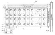
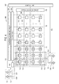
- a solid-state imaging device 100 includes a first region 10 , a second region 11 , a vertical scanning circuit 102 , a column circuit 103 , a horizontal scanning circuit 104 , an output circuit 115 , a control unit 107 , a voltage supply unit 12 , and a voltage switch 13 .
- the first region 10 a first group of pixels 105 and a second group of pixels 106 are arranged over a plurality of rows and a plurality of columns.
- the first region 10 is a pixel region used for image acquisition in which pixels used for image acquisition (image acquisition pixels) are arranged.
- Each of the pixels 105 is a pixel including a photoelectric converter and is illustrated with a white block in FIG. 1 .
- Each of the pixels 106 is a pixel including a light-shielded photoelectric converter and is illustrated with a diagonally hatched block in FIG. 1 .
- Each of the pixels 106 is a pixel that outputs a reference signal that is the reference of a black level and typically arranged in the peripheral edge of the first region 10 . Note that the pixels 106 may not necessarily be provided.
- a third group of pixels 110 and a fourth group of pixels 111 are arranged over a plurality of rows and a plurality of columns.
- the second region 11 is a pixel region used for failure detection in which pixels used for failure detection (detection pixels) are arranged.
- Each of the pixels 110 is a pixel that outputs a signal in accordance with a fixed voltage V 0 and is illustrated with a block with inscribed “V 0 ” in FIG. 1 .
- Each of the pixels 111 is a pixel that outputs a signal in accordance with a fixed voltage V 1 and is illustrated with a block with inscribed “V 1 ” in FIG. 1 .
- the first region 10 and the second region 11 are arranged adjacent in the row direction (the horizontal direction in FIG. 1 ), and the first region 10 and the second region 11 are arranged in the same row but in different columns.
- a pixel control line 109 extending in the row direction is arranged.
- the pixel control line 109 on each row is a signal line common to the pixels 105 , 106 , 110 , and 111 on the corresponding row.
- the pixel control lines 109 are connected to the vertical scanning circuit 102 .
- a vertical output line 108 extending in the column direction is arranged.
- the vertical output line 108 on each column of the first region 10 is a signal line common to the pixels 105 and 106 on the corresponding column.
- the vertical output line 108 on each column of the second region 11 is a signal line common to the pixels 110 and 111 on the corresponding column.
- the vertical output lines 108 are connected to the column circuit 103 .
- the vertical scanning circuit 102 supplies predetermined control signals for driving the pixels 105 , 106 , 110 , and 111 via the pixel control lines 109 .
- Logic circuits such as a shift resistor, an address decoder, or the like may be used for the vertical scanning circuit 102 . While FIG. 1 depicts the pixel control line 109 on each row as a single signal line, a plurality of control signal lines are included in an actual implementation.
- the pixels 105 , 106 , 110 , and 111 on a row selected by the vertical scanning circuit 102 operate to simultaneously output signals to the associated vertical output lines 108 .
- the column circuit 103 amplifies pixel signals output to the vertical output lines 108 and performs a correlated double sampling process on the amplified pixel signals based on a signal at reset operation and a signal at photoelectric conversion.
- a correlated double sampling process based on a signal at reset operation and a signal at input operation of a fixed voltage in a similar manner to the process of the pixels 105 and 106 used for image acquisition.
- the horizontal scanning circuit 104 supplies, to the column circuit 103 , control signals for transferring pixel signals processed in the column circuit 103 to the output circuit 115 sequentially on a column basis.
- the output circuit 115 is formed of a buffer amplifier, a differential amplifier, or the like and outputs, to a signal processing unit (not illustrated) outside the solid-state imaging device 100 , a pixel signal transferred from the column circuit 103 .
- a signal processing unit not illustrated
- an AD conversion unit may be provided to the column circuit 103 or the output circuit 115 to output a digital image signal to the outside.
- the voltage supply unit 12 is a power source circuit that supplies predetermined voltages, for example, the fixed voltages V 0 and V 1 .
- the voltage switch 13 is a switch that switches a conductive state and a non-conductive state of an electrical path between the voltage supply unit 12 and the pixels 110 and 111 of the second region 11 and includes switches SW 0 and SW 1 .
- the switch SW 0 is provided between a supply terminal of the fixed voltage V 0 of the voltage supply unit 12 and a voltage supply line 112 and supplies the fixed voltage V 0 to the voltage supply line 112 in accordance with a control signal (VPD_ON) supplied from the control unit 107 via a control signal line 114 .
- VPD_ON control signal supplied from the control unit 107 via a control signal line 114 .
- the switch SW 1 is provided between a supply terminal of the fixed voltage V 1 of the voltage supply unit 12 and a voltage supply line 113 and supplies the fixed voltage V 1 to the voltage supply line 113 in accordance with a control signal (VPD_ON) supplied from the control unit 107 via a control signal line 114 .
- VPD_ON a control signal supplied from the control unit 107 via a control signal line 114 .
- the voltage supply lines 112 and 113 are interconnections for supplying the fixed voltages V 0 and V 1 from the voltage supply unit 12 to the pixels 110 and 111 arranged in the second region 11 .
- the voltage supply lines 112 and 113 are shared as depicted, for example, which allows for a reduction of the circuit.
- the pixels 110 to which the fixed voltage V 0 is supplied and the pixels 111 to which the fixed voltage V 1 , which is different from the fixed voltage V 0 , is supplied are arranged in a matrix according to a particular pattern.
- the pixels 110 , 110 and 110 are arranged on each column on one row (the lowermost row in FIG. 1 , for example). Further, the pixels 111 , 110 and 111 are arranged on each column on another row (the second row from the bottom in FIG. 1 , for example). That is, the pattern of the fixed voltages applied to the pixels 110 and 111 is different in accordance with the row for the vertical scanning.
- the pixel control line 109 is shared by the pixels 110 and 111 used for failure detection and the pixels 105 and 106 used for image acquisition which all belong to the same row. Therefore, by collating the output pattern in the second region 11 with an expected value, it is possible to detect whether the vertical scanning circuit 102 is operating normally or is scanning a row different from the expectation due to a failure.
- the number of columns that form the second region 11 is not limited to three.
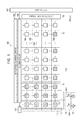
- FIG. 2 is a circuit diagram illustrating an example configuration of the pixels 105 , 106 , 110 , and 111 of the first region 10 and the second region 11 .
- the pixel 105 arranged on the first row and the pixel 106 arranged on the m-th row are extracted from one column of the first region 10
- the pixel 111 arranged on the first row and the pixel 110 arranged on the m-th row are extracted from one column of the second region 11 .
- the circuit configuration of the pixel 105 is the same as the circuit configuration of the pixel 106 .
- Each of the pixels 105 and 106 arranged in the first region 10 includes a photoelectric converter PD, a transfer transistor M 1 , a reset transistor M 2 , an amplifier transistor M 3 , and a select transistor M 4 .
- the photoelectric converter PD is a photodiode, for example.
- the anode of the photodiode of the photoelectric converter PD is connected to a reference voltage terminal GND, and the cathode thereof is connected to the source of the transfer transistor M 1 .
- the drain of the transfer transistor M 1 is connected to the source of the reset transistor M 2 and the gate of the amplifier transistor M 3 .
- connection node of the drain of the transfer transistor M 1 , the source of the reset transistor M 2 , and the gate of the amplifier transistor M 3 forms a floating diffusion FD.
- the drain of the reset transistor M 2 and the drain of the amplifier transistor M 3 are connected to a power source voltage terminal VDD.
- the source of the amplifier transistor M 3 is connected to the drain of the select transistor M 4 .
- the source of the select transistor M 4 is connected to the vertical output line 108 .
- the pixel 110 arranged in the second region 11 includes a transfer transistor M 1 , a reset transistor M 2 , an amplifier transistor M 3 , and a select transistor M 4 .
- the source of the transfer transistor M 1 is connected to the voltage supply line 112 .
- the drain of the transfer transistor M 1 is connected to the source of the reset transistor M 2 and the gate of the amplifier transistor M 3 .
- the connection node of the drain of the transfer transistor M 1 , the source of the reset transistor M 2 , and the gate of the amplifier transistor M 3 forms a floating diffusion FD.
- the drain of the reset transistor M 2 and the drain of the amplifier transistor M 3 are connected to the power source voltage terminal VDD.
- the source of the amplifier transistor M 3 is connected to the drain of the select transistor M 4 .
- the source of the select transistor M 4 is connected to the vertical output line 108 .
- the pixel 111 arranged in the second region 11 is similar to the pixel 110 except that the source of the transfer transistor M 1 is connected to the voltage supply line 113 instead of the voltage supply line 112 .
- the pixel control line 109 arranged on each row includes signal lines TX, RES, and SEL.
- Each of the signal lines TX is connected to the gates of the transfer transistors M 1 of the pixels 105 , 106 , 110 , and 111 belonging to the associated row.
- Each of the signal lines RES is connected to the gates of the reset transistors M 2 of the pixels 105 , 106 , 110 , and 111 belonging to the associated row, respectively.
- Each of the signal lines SEL is connected to the gates of the select transistors M 4 of the pixels 105 , 106 , 110 , and 111 belonging to the associated row, respectively.
- the row number is added to each reference symbol of the signal lines (for example, SEL( 1 ), RES(m)).
- a control signal PTX which is the drive pulse for controlling the transfer transistor M 1 , is output to the signal line TX from the vertical scanning circuit 102 .
- a control signal PRES which is the drive pulse for controlling the reset transistor M 2 , is output to the signal line RES from the vertical scanning circuit 102 .
- a control signal PSEL which is the drive pulse for controlling the select transistor M 4 , is output to the signal line SEL from the vertical scanning circuit 102 .
- the photoelectric converter PD converts (photoelectrically converts) an incident light into charges whose amount is in accordance with the light amount of the incident light and accumulates the generated charges.
- the transfer transistors M 1 of the pixels 105 and 106 transfer the charges of the photoelectric converter PD to the floating diffusion FD.
- the floating diffusion FD is set to a voltage in accordance with the amount of charges transferred from the photoelectric converter PD by charge-to-voltage conversion according to the capacitance component of the floating diffusion FD.
- the transfer transistors M 1 of the pixels 110 and 111 apply, to the floating diffusion FD, voltages supplied from the voltage supply lines 112 and 113 .
- the amplifier transistor M 3 is configured such that the drain thereof is supplied with the power source voltage and the source thereof is supplied with a bias current from a current source (not illustrated) via the select transistor M 4 , and thereby an amplification unit (a source follower circuit) whose gate is an input node is configured. This causes the amplifier transistor M 3 to output a signal based on the voltage of the floating diffusion FD to the vertical output line 108 via the select transistor M 4 .
- the reset transistor M 2 resets the floating diffusion FD to a voltage in accordance with the power source voltage VDD.
- the common control signals PTX, PRES, and PSEL are supplied to the first region 10 and the second region 11 from the vertical scanning circuit 102 .
- the control signals PTX(m), PSEL(m), and PRES(m) are supplied to the transfer transistor M 1 , the reset transistor M 2 , and the select transistor M 4 , respectively, of the pixels 105 , 106 , 110 , and 111 on the m-th row.
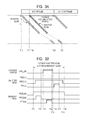
- FIG. 3A is a timing diagram illustrating the relationship between readout scan and shutter scan in one frame period.
- FIG. 3B is a timing diagram illustrating details of the operation of pixels in the scan of a readout scan row and a shutter scan row.
- FIG. 3A schematically illustrates the operation of the N-th frame that starts at the time T 10 and ends at the time T 20 and the (N+1)-th frame that starts at the time T 20 .
- the operation of each frame includes readout scan in which readout operations from the pixels 105 , 106 , 110 , and 111 are sequentially performed on a row basis and shutter scan in which charge accumulation operations to the photoelectric converters PD of the pixels 105 and 106 are sequentially started on a row basis.
- the readout scan of the N-th frame starts at the time T 10 and ends at the time T 20 .
- the time T 10 is the start time of the readout operation from the pixels 105 , 106 , 110 , and 111 on the first row
- the time T 20 is the end time of the readout operation from the pixels 105 , 106 , 110 , and 111 on the last row.
- the shutter scan of the N-th frame starts at the time T 11 and ends at the time T 21 .
- the time T 11 is the start time of the shutter operation in the pixels 105 and 106 on the first row
- the time T 21 is the end time of the shutter operation in the pixels 105 and 106 on the last row.
- a period from the start time of the shutter operation to the start time of the next readout operation is a charge accumulation period.
- the period from the time T 11 to the time T 20 is a charge accumulation period.
- the readout operation from the pixels 105 , 106 , 110 , and 111 on the m-th row starts at the time T 11 at which the shutter operation of the pixels 105 and 106 on the first row starts.
- the shutter operation of the pixels 105 and 106 on the first row and the readout operation from the pixels 105 , 106 , 110 , and 111 on the m-th row end at the time T 19 .
- FIG. 3B illustrates details of the operation of the pixels 105 , 106 , 110 , and 111 from the time T 11 to the time T 19 . Note that the operations of the pixels 105 , 106 , 110 , and 111 are the same as each other in the shutter operation and are the same as each other in the readout operation.
- the control signal PSEL(m) of the readout scan row (the m-th row) becomes a high level, and the select transistors M 4 of the pixels 105 , 106 , 110 , and 111 on the readout scan row are turned on. This operation results in a state where the readout of signals from the pixels 105 , 106 , 110 , and 111 on the readout scan row to the vertical output line 108 is enabled.
- the control signal PRES( 1 ) of the shutter scan row (first row) and the control signal PRES (m) of the readout scan row become a high level.
- This operation causes the reset transistors M 2 of the pixels 105 , 106 , 110 , and 111 on the shutter scan row and the readout scan row to be turned on, and the floating diffusion FD is reset.
- the control signal PRES(m) of the readout scan row becomes a low level, and the reset transistors M 2 of the pixels 105 , 106 , 110 , and 111 on the readout scan row are turned off.
- This operation causes charges present in the floating diffusion FD to be drained to the power source voltage terminal VDD, and the voltage of the floating diffusion FD is amplified by the source follower operation and read out to the vertical output line 108 .
- the control signal VPD_ON becomes a high level and thereby the switches SW 0 and SW 1 of the voltage switch 13 are turned on, and the fixed voltages V 0 and V 1 are supplied to the voltage supply lines 112 and 113 from the voltage supply unit 12 , respectively.
- the control signal PTX(m) of the readout scan row becomes a high level, and the transfer transistors M 1 of the pixels 105 , 106 , 110 , and 111 on the readout scan row are turned on.
- This operation causes charges accumulated in the photoelectric converters PD to be transferred to the floating diffusions FD in the pixels 105 and 106 on the readout scan row.
- the fixed voltages V 0 and V 1 supplied from the voltage supply unit 12 are written to the floating diffusions FD.
- the control signal PTX(m) of the readout scan row becomes a low level
- the transfer transistors M 1 of the pixels 105 , 106 , 110 , and 111 on the readout scan row are turned off. This operation causes the voltages of the floating diffusions FD on the readout scan row to be fixed, and the fixed voltage is amplified by a source follower operation and read out to the vertical output line 108 .
- the control signal VPD_ON becomes a low level and thereby the switches SW 0 and SW 1 of the voltage switch 13 are turned off, which stops the supply of the fixed voltages V 0 and V 1 to the voltage supply lines 112 and 113 from the voltage supply unit 12 .
- the control signal PTX( 1 ) of the shutter scan row becomes a high level, and the transfer transistors M 1 of the pixels 105 , 106 , 110 , and 111 on the shutter scan row are turned on.
- the reset transistors M 2 of the pixels 105 , 106 , 110 , and 111 on the shutter scan row are already turned on, the charges of the photoelectric converters PD are drained to the power source voltage terminal VDD via the transfer transistors M 1 and the reset transistors M 2 .
- the control signal PTX( 1 ) of the shutter scan row becomes a low level, and the transfer transistors M 1 of the pixels 105 , 106 , 110 , and 111 on the shutter scan row are turned off.
- the control signal PRES( 1 ) of the shutter scan row becomes a low level, and the reset transistors M 2 of the pixels 105 , 106 , 110 , and 111 on the shutter scan row are turned off. This operation causes the shutter operation of the shutter scan row to end.
- the control signal PSEL(m) of the readout scan row becomes a low level, and the select transistors M 4 of the pixels 105 , 106 , 110 , and 111 on the readout scan row are turned off. This operation causes the selection of the pixels on the readout scan row to be cancelled, and the readout operation of the readout scan row ends.
- the switches SW 0 and SW 1 of the voltage switch 13 are in an off-state (the control signal VPD_ON is in a low level) while the transfer transistors M 1 of the shutter scan row are in an on-state.
- the fixed voltage terminals V 1 and V 0 and the power source voltage terminal VDD would be short-circuited.
- the fixed voltage V 1 is around 1.6 V and the power source voltage VDD is 3.3V, a flow of the short-circuit current may cause an adverse effect such as incorrect readout of the potentials of the pixels 110 and 111 of the second region 11 .
- the present embodiment is configured such that the voltage switch 13 is provided between the voltage supply unit 12 and the pixels 110 and 111 of the second region 11 . Further, when the transfer transistors M 1 on the shutter scan row are turned on, the switches SW 0 and SW 1 of the voltage switch 13 are driven to be turned off.
- the embodiment is not necessarily limited to such an operation. That is, the timing of turning on the transfer transistors M 1 on the shutter scan row may be earlier than the timing of turning on the transfer transistors M 1 on the readout scan row.
- FIG. 4 A solid-state imaging device and a method of driving the same according to a second embodiment of the present invention will be described by using FIG. 4 .
- the same reference symbols are provided to components similar to those of the solid-state imaging device according to the first embodiment, and the description thereof will be omitted or simplified.
- FIG. 4 is a block diagram illustrating a schematic configuration of a solid-state imaging device according to the present embodiment.
- the solid-state imaging device 100 includes two sets of the voltage supply unit 12 and the voltage switch 13 .
- One of the two sets of the voltage supply unit 12 and the voltage switch 13 supplies the fixed voltages V 0 and V 1 to one group of the pixels 110 and 111 of the second region 11 , such as the pixels 110 and 111 belonging to rows of the upper half part of the second region 11 , for example.
- the other of the two sets of the voltage supply unit 12 and the voltage switch 13 supplies the fixed voltages V 0 and V 1 to the other group of the pixels 110 and 111 of the second region 11 , such as the pixels 110 and 111 belonging to rows of the lower half part of the second region 11 , for example.
- the two voltage switches 13 may be simultaneously controlled by a single control signal VPD_ON or may be separately controlled by different control signals VPD_ON in accordance with rows to be driven.
- the number of the voltage supply unit 12 may be one.
- the fixed voltages V 0 and V 1 are supplied to the two voltage switches 13 from the single voltage supply unit 12 .
- three or more sets of the voltage supply units 12 and the voltage switches 13 may be provided.
- the solid-state imaging device can prevent a short-circuit among the voltage terminals to improve the detection accuracy of failure detection while simultaneously performing capturing and failure detection.
- the pixels belonging to the second region are divided into a plurality of groups, and the voltage supply unit and the voltage switch are provided to each group, which can enhance the capability of voltage supply to the pixels used for failure detection.
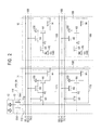
- a solid-state imaging device and a method of driving the same according to a third embodiment of the present invention will be described by using FIG. 5 to FIG. 6B .
- the same reference symbols are provided to components similar to those of the solid-state imaging device according to the first and second embodiments, and the description thereof will be omitted or simplified.
- FIG. 5 is a block diagram illustrating a general configuration of a solid-state imaging device according to the present embodiment.
- FIG. 6A and FIG. 6B are diagrams illustrating an example configuration of a voltage switch in the solid-state imaging device according to the present embodiment.
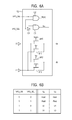
- the solid-state imaging device 100 according to the present embodiment is different from the solid-state imaging device according to the first embodiment in that two voltage switches 13 are provided to one voltage supply unit (first difference). Further, there is a difference from the solid-state imaging device of the first embodiment in that the voltage switch 13 has not only the function of turning on/off the supply of the fixed voltages V 0 and V 1 but also a function of switching the fixed voltages V 0 and V 1 (voltage-switching function) (second difference).
- the solid-state imaging device of the present embodiment is configured such that the voltage switches 13 are arranged above and below the second region 11 and the fixed voltages V 0 and V 1 are supplied to the same voltage supply lines 112 and 113 from the upper and lower voltage switches 13 . That is, the two voltage switches 13 connected in parallel are provided between the voltage supply unit 12 and the voltage supply lines 112 and 113 .
- the configuration that supplies the voltage from both of the upper side and the lower side of the second region 11 has advantages of a reduction in delay of voltage stabilization after switching due to the interconnection capacitance and a reduction in an effect of voltage drop due to the interconnection resistance.
- the fixed voltages V 0 and V 1 cannot be applied.
- the fixed voltages V 0 and V 1 can be applied via the voltage switch 13 which is not failed. This allows for an advantage of not losing the function of the pixels 110 and 111 used for failure detection.
- each of the voltage switches 13 may be of the same configuration as that in the first embodiment.
- the solid-state imaging device of the present embodiment is different from the solid-state imaging device of the first embodiment in the circuit configuration of the voltage switch 13 .
- control signal VPD_SEL in addition to the control signal VPD_ON is used as a control signal supplied to the voltage switches 13 from the control unit 107 .
- the voltage switch 13 is configured such that the fixed voltages V 0 and V 1 are output when the control signal VPD_ON is a high level and the fixed voltages V 0 and V 1 output to terminals Va and Vb are switched in accordance with the level of the control signal VPD_SEL at this time.
- the voltage switch 13 illustrated in FIG. 6A is formed of a NOT gate G 1 , AND gates G 2 and G 3 , and MOS transistors M 10 , M 11 , M 12 , and M 13 .
- the fixed voltage V 0 is supplied to the drains of the MOS transistors M 10 and M 12 .
- the source of the MOS transistor M 10 is connected to the drain of the MOS transistor M 11 .
- the source of the MOS transistor M 12 is connected to the drain of the MOS transistor M 13 .
- the fixed voltage V 1 is supplied to the sources of the MOS transistors M 11 and M 13 .
- the connection node of the source of the MOS transistor M 10 and the drain of the MOS transistor M 11 forms the terminal Va.
- the connection node of the source of the MOS transistor M 11 and the drain of the MOS transistor M 13 forms the terminal Vb.
- the control signal VPD_ON is input to one of the input terminals of the AND gate G 2 and one of the input terminals of the AND gate G 3 .
- the control signal VPD_SEL is input to the other input terminal of the AND gate G 2 and the input terminal of the NOT gate G 1 .
- the output of the NOT gate is input to the other input terminal of the AND gate G 3 .
- An output signal Norm of the AND gate G 2 is a control signal supplied to the gates of the MOS transistors M 10 and M 13 .
- An output signal Inv of the AND gate G 3 is a control signal supplied to the gates of the MOS transistors M 11 and M 12 .
- FIG. 6B is a truth table indicating the relationship between the control signals VPD_ON and VPD_SEL and the voltage output to the terminals Va and Vb in the circuit of FIG. 6A .
- the control signal VPD_ON is a low level (0)
- the terminals Va and Vb are in a floating state regardless of the level of the control signal VPD_SEL.
- the control signal VPD_ON is a high level (1)
- the control signal VPD_SEL is a low level (0)
- the fixed voltage V 0 is output from the terminal Va
- the fixed voltage V 1 is output from the terminal Vb.
- the control signal VPD_ON is a high level (1) and the control signal VPD_SEL is a high level (1)
- the fixed voltage V 1 is output from the terminal Va and the fixed voltage V 0 is output from the terminal Vb.
- the control signal VPD_SEL is set to a high level to drive the control signal VPD_ON as illustrated in FIG. 3B . Further, at the time of readout scan in another frame, the control signal VPD_SEL is set to a low level to drive the control signal VPD_ON as illustrated in FIG. 3B .
- This drive enables detection of a failure even in a failure mode which would otherwise cause false detection that identifies a failure as normal because the pixels 110 and 111 are accidentally fixed to a voltage close to the fixed voltage V 0 , for example.
- the solid-state imaging device can prevent a short-circuit among the voltage terminals to improve the detection accuracy of failure detection while simultaneously performing capturing and failure detection. Further, by switching the fixed voltages supplied to the pixels used for the failure detection, it is possible to reduce a false that would otherwise identify a failure as a normal operation.
- FIG. 7A to FIG. 8 An imaging system and a movable object according to the fourth embodiment of the present invention will be described by using FIG. 7A to FIG. 8 .
- FIG. 7A is a schematic diagram illustrating an example configuration of an imaging system according to the present embodiment.
- FIG. 7B is a schematic diagram illustrating an example configuration of a movable object according to the present embodiment.
- FIG. 8 is a flow diagram illustrating the operation of the imaging system according to the present embodiment.
- FIG. 7A and FIG. 7B illustrate an example of a vehicle system and the imaging system mounted thereon.
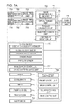
- the imaging system 701 includes an imaging device 702 , an image pre-processing unit 715 , an integrated circuit 703 , and an optical system 714 .
- the optical system 714 forms an optical image of an object on the imaging device 702 .
- the imaging device 702 converts an optical image of an object formed by the optical system 714 into an electrical signal.
- the imaging device 702 is any of the solid-state imaging devices of the first to third embodiments described above.
- the image pre-processing unit 715 performs predetermined signal processing on a signal output from the imaging device 702 .
- the function of the image pre-processing unit 715 may be embedded in the imaging device 702 . At least two sets of the optical system 714 , the imaging device 702 , and the image pre-processing unit 715 are provided in the imaging system 701 , and outputs from the image pre-processing unit 715 of respective sets are input to the integrated circuit 703 .
- the integrated circuit 703 is an application specific integrated circuit for the imaging system and includes an image processing unit 704 including a memory 705 , an optical ranging unit 706 , a parallax calculation unit 707 , an object recognition unit 708 , and an abnormality detection unit 709 .
- the image processing unit 704 performs image processing such as development process, defect correction, or the like on the output signal from the image pre-processing unit 715 .
- the memory 705 stores primary storage data of a captured image or a defection position of a captured image.
- the optical ranging unit 706 performs focusing or ranging of an object.
- the parallax calculation unit 707 calculates a parallax (a phase difference of parallax images) from a plurality of image data acquired by the plurality of imaging devices 702 .
- the object recognition unit 708 recognizes an object such as an automobile, a road, a traffic sign, a person, or the like.
- the abnormality detection unit 709 reports the abnormality to a main control unit 713 . Note that the report of an abnormality may be performed outward the vehicle system. For example, an abnormality may be reported to a wireless network connected to the vehicle system.
- the integrated circuit 703 may be implemented by dedicatedly designed hardware, may be implemented by a software module, or may be implemented by the combination thereof. Further, the integrated circuit 703 may be implemented by a Field Programmable Gate Array (FPGA), an Application Specific Integrated Circuit (ASIC), or the like, or may be implemented by the combination thereof.
- FPGA Field Programmable Gate Array
- ASIC Application Specific Integrated Circuit
- the main control unit 713 organizes and controls the operation of the imaging system 701 , a vehicle sensor 710 , a control unit 720 , or the like. Note that such a method may be employed that the imaging system 701 , the vehicle sensor 710 , and the control unit 720 have separate communication interfaces without the main control unit 713 and transmit and receive control signals respectively via the communication network (for example, CAN specification).
- the communication network for example, CAN specification
- the integrated circuit 703 has a function of transmitting a control signal or a setting value to the imaging device 702 in response to receiving the control signal from the main control unit 713 or by using a control unit of the integrated circuit 703 .
- the integrated circuit 703 transmits a setting for pulse-driving the voltage switch 13 in the imaging device 702 , a setting for switching the voltage switches 13 on a frame basis, or the like.
- the imaging system 701 is connected to the vehicle sensor 710 and can sense a traveling state of the vehicle, such as a vehicle speed, a yaw rate, a steering angle, or the like, and a state of an environment outside the vehicle or another vehicle and an obstacle.
- the vehicle sensor 710 also serves as a distance information acquisition unit that acquires information on the distance from the parallax image to the object.
- the imaging system 701 is connected to a drive support control unit 711 that performs various drive supports such as steering, patrol, collision prevention function, or the like.
- the collision prevention function collision estimation and a collision against another vehicle and an obstacle is determined based on the sensing result of the imaging system 701 or the vehicle sensor 710 . Thereby, avoidance control when a collision is estimated or startup of a safety device at a collision is performed.
- the imaging system 701 is connected to an alert device 712 that issues an alert to a driver based on the determination result in a collision determination unit.
- the main control unit 713 performs vehicle control to avoid a collision or reduce damage by applying a break, moving back the accelerator pedal, suppressing the engine power, or the like.
- the alert device 712 performs an alert to a user by sounding an alert such as a sound, displaying alert information on a display unit such as a car navigation system, a meter panel, or the like, providing a vibration to a seat belt or a steering wheel.
- the surrounding area of the vehicle for example, the area in front or rear is captured by the imaging system 701 .
- FIG. 7B illustrates an example arrangement of an imaging system 701 when the area in front of the vehicle is captured by the imaging system 701 .
- Two imaging devices 702 are arranged in the front of the vehicle 700 .
- the center line with respect to the traveling direction or the external shape (for example, the vehicle width) of the vehicle 700 as a symmetry axis and arrange the two imaging devices 702 in a symmetrical manner with respect to the symmetry axis.
- the imaging devices 702 so as not to block the driver's field of view when the driver views the surroundings outside the vehicle 700 out of the driver seat. It is preferable to arrange the alert device 712 so as to be easily viewed by the driver.
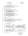
- the failure detection operation of the imaging device 702 in the imaging system 701 will be described by using FIG. 8 .
- the failure detection operation of the imaging device 702 is performed according to steps S 810 to S 880 illustrated in FIG. 8 .
- Step S 810 is a step of performing setting at startup of the imaging devices 702 . That is, a setting for the operation of the imaging devices 702 is transmitted from the outside of the imaging system 701 (for example, the main control unit 713 ) or the inside of the imaging system 701 to start a capturing operation and a failure detection operation of the imaging devices 702 .
- the setting for the operation of the imaging devices 702 includes a setting for control of the voltage switch 13 .
- step S 820 signals from the pixels 105 and 106 of the first region 10 belonging to a scanning row are acquired. Further, at step S 830 , output values from the pixels 110 and 111 of the second region 11 belonging to the scanning row are acquired. Note that step S 820 and step S 830 may be exchanged.
- step S 840 classification is performed between output expectation values of pixels 110 and 111 based on connection settings of the fixed voltages V 0 and V 1 to the pixels 110 and 111 and the actual output values from the pixels 110 and 111 .
- step S 850 is entered to determine that the capturing operation in the first region 10 is normally performed, and step S 860 is entered.
- step S 860 pixel signals on the scanning rows are transmitted to the memory 705 and temporarily saved therein. The process then returns to step S 820 and continues the failure detection operation.
- step S 870 is entered to determine that there is an abnormality in the capturing operation in the first region 10 , and reports an alert to the main control unit 713 or the alert device 712 .
- the alert device 712 causes the display unit to display that an abnormality has been detected.
- the imaging devices 702 are then stopped at step S 880 to end the operation of the imaging system 701 .
- the flowchart may be looped on a multiple-row basis, or the failure detection operation may be performed on a frame basis.
- the embodiment is applicable to driving control for following another vehicle, driving control for not going out of a traffic lane, or the like.
- the imaging system 701 is not limited to a vehicle such as the subject vehicle, and can be applied to a movable object (moving apparatus) such as a ship, an airplane, or an industrial robot, for example.
- the imaging system 701 can be widely applied to a device which utilizes object recognition, such as an intelligent transportation system (ITS), without being limited to movable objects.
- ITS intelligent transportation system
- the embodiments of the present invention include an example in which a part of the configuration of one of the embodiments is added to another embodiment or an example in which a part of the configuration of one of the embodiments is replaced with a part of the configuration of another embodiment.
- each transistor of the pixels 105 , 106 , 110 , and 111 is formed of an n-channel transistor
- each transistor of the pixels 105 , 106 , 110 , and 111 may be formed of a p-channel transistor.
- the signal level of each drive signal in the above description is inverted.
- each circuit configuration of the pixels 105 , 106 , 110 , and 111 is not limited to that illustrated in FIG. 2 , and can be properly changed.
- each of the pixels 105 , 106 , 110 , and 111 may have the dual pixel structure having two photoelectric converters for a single pixel.
- the imaging system illustrated in the fourth embodiment has been illustrated as an example imaging system to which the solid-state imaging device of the present invention can be applied, the imaging system to which the solid-state imaging device of the present invention can be applied is not limited to the configuration illustrated in FIG. 7A and FIG. 8 .
- the solid-state imaging devices described in the above first to third embodiments can be applied to a digital still camera, a digital camcorder, a surveillance camera, or the like.
Landscapes
- Engineering & Computer Science (AREA)
- Multimedia (AREA)
- Signal Processing (AREA)
- Physics & Mathematics (AREA)
- Electromagnetism (AREA)
- Health & Medical Sciences (AREA)
- Biomedical Technology (AREA)
- General Health & Medical Sciences (AREA)
- Transforming Light Signals Into Electric Signals (AREA)
- Solid State Image Pick-Up Elements (AREA)
- Studio Devices (AREA)
Abstract
Description
- The present invention relates to a solid-state imaging device, a method of driving the solid-state imaging device, and an imaging system.
- In recent years, there is a demand for reduction in size and improvement of reliability of a solid-state imaging device. In particular, the safety measure is quite important in on-vehicle applications under a severe operating environment and, for a functional safety, there is a demand for an imaging system with a failure detection function. To address this, it is required to embed a mechanism for failure detection also in a solid-state imaging device.
- International Publication No. WO2006/120815 discloses, as a solid-state imaging device having means for failure detection, a solid-state imaging device configured such that means for generating a reference signal is provided in addition to a photoelectric converter in each pixel to output the reference signal. When the level of the output reference signal is compared to an expected value and the comparison result is out of the expected range, it can be determined that the solid-state imaging device is malfunctioning.
- Reset operations of nodes may be performed in parallel on a pixel in which charges obtained by photoelectric conversion are input to the node via a transfer transistor and on a pixel in which a predetermined voltage is input to the node via a transfer transistor. In the solid-state imaging device disclosed in International Publication No. WO2006/120815, however, there is no consideration for the relationship between the reset operations of the node and the operation for inputting a predetermined voltage to the node in the above case.
- The present invention intends to improve the accuracy of failure detection in a solid-state imaging device and an imaging system that can detect a failure while performing capturing.
- According to one aspect of the present invention, there is provided a solid-state imaging device including a first detection pixel and a second detection pixel, each of the first and second detection pixels including a transfer transistor and an amplifier transistor connected to the transfer transistor via a first node, a voltage supply unit that supplies a predetermined voltage, and a connection switch connected between the voltage supply unit and a second node at which the transfer transistor of the first detection pixel and the transfer transistor of the second detection pixel are connected.
- According to further another aspect of the present invention, there is provided a method of driving a solid-state imaging device including a voltage supply unit that supplies a predetermined voltage, a first detection pixel, a second detection pixel, and a control line, wherein the first detection pixel includes a photoelectric converter, a first transfer transistor connected to the photoelectric converter, and a first reset transistor connected to the first transfer transistor, wherein the second detection pixel includes a second transfer transistor and a second reset transistor connected to the second transfer transistor, and wherein the control line is connected to a gate of the first transfer transistor and a gate of the second transfer transistor, the method including setting an electrical path between the voltage supply unit and the second transfer transistor to be non-conductive in at least a part of a period in which the control line has a potential that causes both of the first transfer transistor and the first reset transistor to be turned on.
- Further features of the present invention will become apparent from the following description of exemplary embodiments with reference to the attached drawings.
-
FIG. 1 is a block diagram illustrating a general configuration of a solid-state imaging device according to a first embodiment of the present invention. -
FIG. 2 is a circuit diagram illustrating an example configuration of pixels in the solid-state imaging device according to the first embodiment of the present invention. -
FIG. 3A andFIG. 3B are timing diagrams illustrating a method of driving the solid-state imaging device according to the first embodiment of the present invention. -
FIG. 4 is a block diagram illustrating a general configuration of a solid-state imaging device according to a second embodiment of the present invention. -
FIG. 5 is a block diagram illustrating a general configuration of a solid-state imaging device according to a third embodiment of the present invention. -
FIG. 6A andFIG. 6B are diagrams illustrating an example configuration of a voltage switch in the solid-state imaging device according to the third embodiment of the present invention. -
FIG. 7A is a schematic diagram illustrating an example configuration of an imaging system according to a fourth embodiment of the present invention. -
FIG. 7B is a schematic diagram illustrating an example configuration of a movable object according to the fourth embodiment of the present invention. -
FIG. 8 is a flow diagram illustrating the operation of the imaging system according to the fourth embodiment of the present invention. - Preferred embodiments of the present invention will now be described in detail in accordance with the accompanying drawings.
- A solid-state imaging device and a method of driving the same according to a first embodiment of the present invention will be described by using
FIG. 1 toFIG. 3B . -
FIG. 1 is a block diagram illustrating a general configuration of the solid-state imaging device according to the present embodiment.FIG. 2 is a circuit diagram illustrating an example configuration of pixels in the solid-state imaging device according to the present embodiment.FIG. 3A andFIG. 3B are timing diagrams illustrating the method of driving the solid-state imaging device according to the present embodiment. - First, the structure of the solid-state imaging device according to the present embodiment will be described by using
FIG. 1 andFIG. 2 . - As illustrated in
FIG. 1 , a solid-state imaging device 100 according to the present embodiment includes afirst region 10, asecond region 11, avertical scanning circuit 102, acolumn circuit 103, ahorizontal scanning circuit 104, anoutput circuit 115, acontrol unit 107, avoltage supply unit 12, and avoltage switch 13. - In the
first region 10, a first group ofpixels 105 and a second group ofpixels 106 are arranged over a plurality of rows and a plurality of columns. Thefirst region 10 is a pixel region used for image acquisition in which pixels used for image acquisition (image acquisition pixels) are arranged. Each of thepixels 105 is a pixel including a photoelectric converter and is illustrated with a white block inFIG. 1 . Each of thepixels 106 is a pixel including a light-shielded photoelectric converter and is illustrated with a diagonally hatched block inFIG. 1 . Each of thepixels 106 is a pixel that outputs a reference signal that is the reference of a black level and typically arranged in the peripheral edge of thefirst region 10. Note that thepixels 106 may not necessarily be provided. - In the
second region 11, a third group ofpixels 110 and a fourth group ofpixels 111 are arranged over a plurality of rows and a plurality of columns. Thesecond region 11 is a pixel region used for failure detection in which pixels used for failure detection (detection pixels) are arranged. Each of thepixels 110 is a pixel that outputs a signal in accordance with a fixed voltage V0 and is illustrated with a block with inscribed “V0” inFIG. 1 . Each of thepixels 111 is a pixel that outputs a signal in accordance with a fixed voltage V1 and is illustrated with a block with inscribed “V1” inFIG. 1 . - The
first region 10 and thesecond region 11 are arranged adjacent in the row direction (the horizontal direction inFIG. 1 ), and thefirst region 10 and thesecond region 11 are arranged in the same row but in different columns. - In each row of the
first region 10 and thesecond region 11, apixel control line 109 extending in the row direction is arranged. Thepixel control line 109 on each row is a signal line common to thepixels pixel control lines 109 are connected to thevertical scanning circuit 102. - In each column of the
first region 10 and thesecond region 11, avertical output line 108 extending in the column direction is arranged. Thevertical output line 108 on each column of thefirst region 10 is a signal line common to thepixels vertical output line 108 on each column of thesecond region 11 is a signal line common to thepixels vertical output lines 108 are connected to thecolumn circuit 103. - The
vertical scanning circuit 102 supplies predetermined control signals for driving thepixels pixel control lines 109. Logic circuits such as a shift resistor, an address decoder, or the like may be used for thevertical scanning circuit 102. WhileFIG. 1 depicts thepixel control line 109 on each row as a single signal line, a plurality of control signal lines are included in an actual implementation. Thepixels vertical scanning circuit 102 operate to simultaneously output signals to the associated vertical output lines 108. - The
column circuit 103 amplifies pixel signals output to thevertical output lines 108 and performs a correlated double sampling process on the amplified pixel signals based on a signal at reset operation and a signal at photoelectric conversion. On the pixel signals output from thepixels pixels - The
horizontal scanning circuit 104 supplies, to thecolumn circuit 103, control signals for transferring pixel signals processed in thecolumn circuit 103 to theoutput circuit 115 sequentially on a column basis. - The
output circuit 115 is formed of a buffer amplifier, a differential amplifier, or the like and outputs, to a signal processing unit (not illustrated) outside the solid-state imaging device 100, a pixel signal transferred from thecolumn circuit 103. Note that an AD conversion unit may be provided to thecolumn circuit 103 or theoutput circuit 115 to output a digital image signal to the outside. - The
voltage supply unit 12 is a power source circuit that supplies predetermined voltages, for example, the fixed voltages V0 and V1. Thevoltage switch 13 is a switch that switches a conductive state and a non-conductive state of an electrical path between thevoltage supply unit 12 and thepixels second region 11 and includes switches SW0 and SW1. The switch SW0 is provided between a supply terminal of the fixed voltage V0 of thevoltage supply unit 12 and avoltage supply line 112 and supplies the fixed voltage V0 to thevoltage supply line 112 in accordance with a control signal (VPD_ON) supplied from thecontrol unit 107 via acontrol signal line 114. The switch SW1 is provided between a supply terminal of the fixed voltage V1 of thevoltage supply unit 12 and avoltage supply line 113 and supplies the fixed voltage V1 to thevoltage supply line 113 in accordance with a control signal (VPD_ON) supplied from thecontrol unit 107 via acontrol signal line 114. - The
voltage supply lines voltage supply unit 12 to thepixels second region 11. In the plurality ofpixels second region 11, thevoltage supply lines - In the
second region 11, thepixels 110 to which the fixed voltage V0 is supplied and thepixels 111 to which the fixed voltage V1, which is different from the fixed voltage V0, is supplied are arranged in a matrix according to a particular pattern. - In a case where the
second region 11 is formed of three columns, for example, thepixels FIG. 1 , for example). Further, thepixels FIG. 1 , for example). That is, the pattern of the fixed voltages applied to thepixels - The
pixel control line 109 is shared by thepixels pixels second region 11 with an expected value, it is possible to detect whether thevertical scanning circuit 102 is operating normally or is scanning a row different from the expectation due to a failure. - Note that, while the case where the
second region 11 is formed of three columns is exemplified in the present embodiment, the number of columns that form thesecond region 11 is not limited to three. -
FIG. 2 is a circuit diagram illustrating an example configuration of thepixels first region 10 and thesecond region 11. InFIG. 2 , thepixel 105 arranged on the first row and thepixel 106 arranged on the m-th row are extracted from one column of thefirst region 10, and thepixel 111 arranged on the first row and thepixel 110 arranged on the m-th row are extracted from one column of thesecond region 11. Note that the circuit configuration of thepixel 105 is the same as the circuit configuration of thepixel 106. - Each of the
pixels first region 10 includes a photoelectric converter PD, a transfer transistor M1, a reset transistor M2, an amplifier transistor M3, and a select transistor M4. The photoelectric converter PD is a photodiode, for example. The anode of the photodiode of the photoelectric converter PD is connected to a reference voltage terminal GND, and the cathode thereof is connected to the source of the transfer transistor M1. The drain of the transfer transistor M1 is connected to the source of the reset transistor M2 and the gate of the amplifier transistor M3. The connection node of the drain of the transfer transistor M1, the source of the reset transistor M2, and the gate of the amplifier transistor M3 forms a floating diffusion FD. The drain of the reset transistor M2 and the drain of the amplifier transistor M3 are connected to a power source voltage terminal VDD. The source of the amplifier transistor M3 is connected to the drain of the select transistor M4. The source of the select transistor M4 is connected to thevertical output line 108. - The
pixel 110 arranged in thesecond region 11 includes a transfer transistor M1, a reset transistor M2, an amplifier transistor M3, and a select transistor M4. The source of the transfer transistor M1 is connected to thevoltage supply line 112. The drain of the transfer transistor M1 is connected to the source of the reset transistor M2 and the gate of the amplifier transistor M3. The connection node of the drain of the transfer transistor M1, the source of the reset transistor M2, and the gate of the amplifier transistor M3 forms a floating diffusion FD. The drain of the reset transistor M2 and the drain of the amplifier transistor M3 are connected to the power source voltage terminal VDD. The source of the amplifier transistor M3 is connected to the drain of the select transistor M4. The source of the select transistor M4 is connected to thevertical output line 108. - The
pixel 111 arranged in thesecond region 11 is similar to thepixel 110 except that the source of the transfer transistor M1 is connected to thevoltage supply line 113 instead of thevoltage supply line 112. - In the case of the pixel configuration of
FIG. 2 , thepixel control line 109 arranged on each row includes signal lines TX, RES, and SEL. Each of the signal lines TX is connected to the gates of the transfer transistors M1 of thepixels pixels pixels FIG. 2 , the row number is added to each reference symbol of the signal lines (for example, SEL(1), RES(m)). - A control signal PTX, which is the drive pulse for controlling the transfer transistor M1, is output to the signal line TX from the
vertical scanning circuit 102. A control signal PRES, which is the drive pulse for controlling the reset transistor M2, is output to the signal line RES from thevertical scanning circuit 102. A control signal PSEL, which is the drive pulse for controlling the select transistor M4, is output to the signal line SEL from thevertical scanning circuit 102. When each transistor is formed of an n-channel transistor, the related transistor is turned on when a high-level control signal is supplied from thevertical scanning circuit 102, and the related transistor is turned off when a low-level control signal is supplied from thevertical scanning circuit 102. - The photoelectric converter PD converts (photoelectrically converts) an incident light into charges whose amount is in accordance with the light amount of the incident light and accumulates the generated charges. When turned on, the transfer transistors M1 of the
pixels pixels voltage supply lines vertical output line 108 via the select transistor M4. When turned on, the reset transistor M2 resets the floating diffusion FD to a voltage in accordance with the power source voltage VDD. - With respect to the
pixels first region 10 and thesecond region 11 from thevertical scanning circuit 102. For example, the control signals PTX(m), PSEL(m), and PRES(m) are supplied to the transfer transistor M1, the reset transistor M2, and the select transistor M4, respectively, of thepixels - Next, the method of driving the solid-state imaging device according to the present embodiment will be described by using
FIG. 3A andFIG. 3B .FIG. 3A is a timing diagram illustrating the relationship between readout scan and shutter scan in one frame period.FIG. 3B is a timing diagram illustrating details of the operation of pixels in the scan of a readout scan row and a shutter scan row. -
FIG. 3A schematically illustrates the operation of the N-th frame that starts at the time T10 and ends at the time T20 and the (N+1)-th frame that starts at the time T20. The operation of each frame includes readout scan in which readout operations from thepixels pixels - The readout scan of the N-th frame starts at the time T10 and ends at the time T20. The time T10 is the start time of the readout operation from the
pixels pixels - The shutter scan of the N-th frame starts at the time T11 and ends at the time T21. The time T11 is the start time of the shutter operation in the
pixels pixels - It is assumed here that the readout operation from the
pixels pixels pixels pixels -
FIG. 3B illustrates details of the operation of thepixels pixels - At the time T11, the control signal PSEL(m) of the readout scan row (the m-th row) becomes a high level, and the select transistors M4 of the
pixels pixels vertical output line 108 is enabled. - Next, between the time T11 and the time T12, the control signal PRES(1) of the shutter scan row (first row) and the control signal PRES (m) of the readout scan row become a high level. This operation causes the reset transistors M2 of the
pixels - Next, at the time T12, the control signal PRES(m) of the readout scan row becomes a low level, and the reset transistors M2 of the
pixels vertical output line 108. - Next, at the time T13, the control signal VPD_ON becomes a high level and thereby the switches SW0 and SW1 of the
voltage switch 13 are turned on, and the fixed voltages V0 and V1 are supplied to thevoltage supply lines voltage supply unit 12, respectively. - Next, between the time T13 and the time T14, the control signal PTX(m) of the readout scan row becomes a high level, and the transfer transistors M1 of the
pixels pixels pixels voltage supply unit 12 are written to the floating diffusions FD. - Next, at the time T14, the control signal PTX(m) of the readout scan row becomes a low level, the transfer transistors M1 of the
pixels vertical output line 108. - Next, at the time T15, the control signal VPD_ON becomes a low level and thereby the switches SW0 and SW1 of the
voltage switch 13 are turned off, which stops the supply of the fixed voltages V0 and V1 to thevoltage supply lines voltage supply unit 12. - Next, at the time T16, the control signal PTX(1) of the shutter scan row becomes a high level, and the transfer transistors M1 of the
pixels pixels - Next, at the time T17, the control signal PTX(1) of the shutter scan row becomes a low level, and the transfer transistors M1 of the
pixels pixels - Next, at the time T19, the control signal PSEL(m) of the readout scan row becomes a low level, and the select transistors M4 of the
pixels - In the present embodiment, as described above, the switches SW0 and SW1 of the
voltage switch 13 are in an off-state (the control signal VPD_ON is in a low level) while the transfer transistors M1 of the shutter scan row are in an on-state. The reason for the above will be described below. - In order to completely remove charges of the photoelectric converters PD of the
pixels first region 10 through a shutter operation, it is desirable to simultaneously turn on the reset transistors M2 and the transfer transistors M1 on the shutter scan row. In particular, when the saturated charge amount of the photoelectric converter PD exceeds the saturated charge amount of the floating diffusion FD, it is essential that the reset transistor M2 and the transfer transistor M1 be simultaneously turned on. - However, if voltage supply from the
voltage supply unit 12 to thepixels second region 11 continued in this state, the fixed voltage terminals V1 and V0 and the power source voltage terminal VDD would be short-circuited. Typically, because the fixed voltage V1 is around 1.6 V and the power source voltage VDD is 3.3V, a flow of the short-circuit current may cause an adverse effect such as incorrect readout of the potentials of thepixels second region 11. - To address this, the present embodiment is configured such that the
voltage switch 13 is provided between thevoltage supply unit 12 and thepixels second region 11. Further, when the transfer transistors M1 on the shutter scan row are turned on, the switches SW0 and SW1 of thevoltage switch 13 are driven to be turned off. - This avoids a short-circuit of the fixed voltage terminals V0 and V1 and the power source voltage terminal VDD at the time of shutter scan and allows for a higher detection accuracy of failure detection. That is, by avoiding a short-circuit among the voltage terminals at the time of shutter scan, an advantage of increasing the detection accuracy of failure detection can be obtained while performing capturing and failure detection in a real-time manner.
- Note that, in the present embodiment, although the timing of turning on the transfer transistors M1 on the shutter scan row is later than the timing of turning on the transfer transistors M1 on the readout scan row, the embodiment is not necessarily limited to such an operation. That is, the timing of turning on the transfer transistors M1 on the shutter scan row may be earlier than the timing of turning on the transfer transistors M1 on the readout scan row.
- As discussed above, according to the present embodiment, it is possible to perform capturing and failure detection simultaneously and prevent a short-circuit among voltage terminals to improve the detection accuracy of failure detection.
- A solid-state imaging device and a method of driving the same according to a second embodiment of the present invention will be described by using
FIG. 4 . The same reference symbols are provided to components similar to those of the solid-state imaging device according to the first embodiment, and the description thereof will be omitted or simplified. -
FIG. 4 is a block diagram illustrating a schematic configuration of a solid-state imaging device according to the present embodiment. - The solid-
state imaging device 100 according to the present embodiment includes two sets of thevoltage supply unit 12 and thevoltage switch 13. One of the two sets of thevoltage supply unit 12 and thevoltage switch 13 supplies the fixed voltages V0 and V1 to one group of thepixels second region 11, such as thepixels second region 11, for example. The other of the two sets of thevoltage supply unit 12 and thevoltage switch 13 supplies the fixed voltages V0 and V1 to the other group of thepixels second region 11, such as thepixels second region 11, for example. The twovoltage switches 13 may be simultaneously controlled by a single control signal VPD_ON or may be separately controlled by different control signals VPD_ON in accordance with rows to be driven. - This can enhance the capability of voltage supply to the
second region 11, which can further enhance the accuracy of failure detection while avoiding occurrence of a short-circuit among power source terminals at the time of shutter scan. - Note that, although two
voltage supply units 12 are provided in the present embodiment, the number of thevoltage supply unit 12 may be one. In this case, the fixed voltages V0 and V1 are supplied to the twovoltage switches 13 from the singlevoltage supply unit 12. Further, three or more sets of thevoltage supply units 12 and the voltage switches 13 may be provided. - As discussed above, the solid-state imaging device according to the present embodiment can prevent a short-circuit among the voltage terminals to improve the detection accuracy of failure detection while simultaneously performing capturing and failure detection. Further, the pixels belonging to the second region are divided into a plurality of groups, and the voltage supply unit and the voltage switch are provided to each group, which can enhance the capability of voltage supply to the pixels used for failure detection.
- A solid-state imaging device and a method of driving the same according to a third embodiment of the present invention will be described by using
FIG. 5 toFIG. 6B . The same reference symbols are provided to components similar to those of the solid-state imaging device according to the first and second embodiments, and the description thereof will be omitted or simplified. -
FIG. 5 is a block diagram illustrating a general configuration of a solid-state imaging device according to the present embodiment.FIG. 6A andFIG. 6B are diagrams illustrating an example configuration of a voltage switch in the solid-state imaging device according to the present embodiment. - The solid-
state imaging device 100 according to the present embodiment is different from the solid-state imaging device according to the first embodiment in that twovoltage switches 13 are provided to one voltage supply unit (first difference). Further, there is a difference from the solid-state imaging device of the first embodiment in that thevoltage switch 13 has not only the function of turning on/off the supply of the fixed voltages V0 and V1 but also a function of switching the fixed voltages V0 and V1 (voltage-switching function) (second difference). - In relation to the first difference described above, the solid-state imaging device of the present embodiment is configured such that the voltage switches 13 are arranged above and below the
second region 11 and the fixed voltages V0 and V1 are supplied to the samevoltage supply lines voltage switches 13 connected in parallel are provided between thevoltage supply unit 12 and thevoltage supply lines second region 11 has advantages of a reduction in delay of voltage stabilization after switching due to the interconnection capacitance and a reduction in an effect of voltage drop due to the interconnection resistance. - When the
single voltage switch 13 is employed and when there is an open-circuit failure in thevoltage switch 13, the fixed voltages V0 and V1 cannot be applied. However, when the twovoltage switches 13 are employed, the fixed voltages V0 and V1 can be applied via thevoltage switch 13 which is not failed. This allows for an advantage of not losing the function of thepixels - Note that, when it is sufficient to realize the advantage based on the first difference, each of the voltage switches 13 may be of the same configuration as that in the first embodiment.
- Further, in relation to the second difference described above, the solid-state imaging device of the present embodiment is different from the solid-state imaging device of the first embodiment in the circuit configuration of the
voltage switch 13. - In the present embodiment, the control signal VPD_SEL in addition to the control signal VPD_ON is used as a control signal supplied to the voltage switches 13 from the
control unit 107. Thevoltage switch 13 is configured such that the fixed voltages V0 and V1 are output when the control signal VPD_ON is a high level and the fixed voltages V0 and V1 output to terminals Va and Vb are switched in accordance with the level of the control signal VPD_SEL at this time. - Although the circuit that implements such an operation is not limited in particular, the circuit illustrated in
FIG. 6A may be applied, for example. Thevoltage switch 13 illustrated inFIG. 6A is formed of a NOT gate G1, AND gates G2 and G3, and MOS transistors M10, M11, M12, and M13. - The fixed voltage V0 is supplied to the drains of the MOS transistors M10 and M12. The source of the MOS transistor M10 is connected to the drain of the MOS transistor M11. The source of the MOS transistor M12 is connected to the drain of the MOS transistor M13. The fixed voltage V1 is supplied to the sources of the MOS transistors M11 and M13. The connection node of the source of the MOS transistor M10 and the drain of the MOS transistor M11 forms the terminal Va. The connection node of the source of the MOS transistor M11 and the drain of the MOS transistor M13 forms the terminal Vb.
- The control signal VPD_ON is input to one of the input terminals of the AND gate G2 and one of the input terminals of the AND gate G3. The control signal VPD_SEL is input to the other input terminal of the AND gate G2 and the input terminal of the NOT gate G1. The output of the NOT gate is input to the other input terminal of the AND gate G3. An output signal Norm of the AND gate G2 is a control signal supplied to the gates of the MOS transistors M10 and M13. An output signal Inv of the AND gate G3 is a control signal supplied to the gates of the MOS transistors M11 and M12.
-
FIG. 6B is a truth table indicating the relationship between the control signals VPD_ON and VPD_SEL and the voltage output to the terminals Va and Vb in the circuit ofFIG. 6A . As illustrated inFIG. 6B , when the control signal VPD_ON is a low level (0), the terminals Va and Vb are in a floating state regardless of the level of the control signal VPD_SEL. When the control signal VPD_ON is a high level (1) and the control signal VPD_SEL is a low level (0), the fixed voltage V0 is output from the terminal Va and the fixed voltage V1 is output from the terminal Vb. When the control signal VPD_ON is a high level (1) and the control signal VPD_SEL is a high level (1), the fixed voltage V1 is output from the terminal Va and the fixed voltage V0 is output from the terminal Vb. - As discussed above, by switching the signal level of the control signal VPD_SEL when the control signal VPD_ON is a high level, it is possible to provide two values of the fixed voltage V0 and the fixed voltage V1 to the
same pixels - For example, at the time of readout scan in a certain frame, the control signal VPD_SEL is set to a high level to drive the control signal VPD_ON as illustrated in
FIG. 3B . Further, at the time of readout scan in another frame, the control signal VPD_SEL is set to a low level to drive the control signal VPD_ON as illustrated inFIG. 3B . This drive enables detection of a failure even in a failure mode which would otherwise cause false detection that identifies a failure as normal because thepixels - As discussed above, the solid-state imaging device according to the present embodiment can prevent a short-circuit among the voltage terminals to improve the detection accuracy of failure detection while simultaneously performing capturing and failure detection. Further, by switching the fixed voltages supplied to the pixels used for the failure detection, it is possible to reduce a false that would otherwise identify a failure as a normal operation.
- An imaging system and a movable object according to the fourth embodiment of the present invention will be described by using
FIG. 7A toFIG. 8 . -
FIG. 7A is a schematic diagram illustrating an example configuration of an imaging system according to the present embodiment.FIG. 7B is a schematic diagram illustrating an example configuration of a movable object according to the present embodiment.FIG. 8 is a flow diagram illustrating the operation of the imaging system according to the present embodiment. - In the present embodiment, an example of the imaging system related to an on-vehicle camera is illustrated.
FIG. 7A andFIG. 7B illustrate an example of a vehicle system and the imaging system mounted thereon. Theimaging system 701 includes animaging device 702, animage pre-processing unit 715, anintegrated circuit 703, and anoptical system 714. Theoptical system 714 forms an optical image of an object on theimaging device 702. Theimaging device 702 converts an optical image of an object formed by theoptical system 714 into an electrical signal. Theimaging device 702 is any of the solid-state imaging devices of the first to third embodiments described above. Theimage pre-processing unit 715 performs predetermined signal processing on a signal output from theimaging device 702. The function of theimage pre-processing unit 715 may be embedded in theimaging device 702. At least two sets of theoptical system 714, theimaging device 702, and theimage pre-processing unit 715 are provided in theimaging system 701, and outputs from theimage pre-processing unit 715 of respective sets are input to theintegrated circuit 703. - The
integrated circuit 703 is an application specific integrated circuit for the imaging system and includes animage processing unit 704 including amemory 705, an optical rangingunit 706, aparallax calculation unit 707, anobject recognition unit 708, and anabnormality detection unit 709. Theimage processing unit 704 performs image processing such as development process, defect correction, or the like on the output signal from theimage pre-processing unit 715. Thememory 705 stores primary storage data of a captured image or a defection position of a captured image. The optical rangingunit 706 performs focusing or ranging of an object. Theparallax calculation unit 707 calculates a parallax (a phase difference of parallax images) from a plurality of image data acquired by the plurality ofimaging devices 702. Theobject recognition unit 708 recognizes an object such as an automobile, a road, a traffic sign, a person, or the like. In response to detection of an abnormality of theimaging device 702, theabnormality detection unit 709 reports the abnormality to amain control unit 713. Note that the report of an abnormality may be performed outward the vehicle system. For example, an abnormality may be reported to a wireless network connected to the vehicle system. - The
integrated circuit 703 may be implemented by dedicatedly designed hardware, may be implemented by a software module, or may be implemented by the combination thereof. Further, theintegrated circuit 703 may be implemented by a Field Programmable Gate Array (FPGA), an Application Specific Integrated Circuit (ASIC), or the like, or may be implemented by the combination thereof. - The
main control unit 713 organizes and controls the operation of theimaging system 701, avehicle sensor 710, acontrol unit 720, or the like. Note that such a method may be employed that theimaging system 701, thevehicle sensor 710, and thecontrol unit 720 have separate communication interfaces without themain control unit 713 and transmit and receive control signals respectively via the communication network (for example, CAN specification). - The
integrated circuit 703 has a function of transmitting a control signal or a setting value to theimaging device 702 in response to receiving the control signal from themain control unit 713 or by using a control unit of theintegrated circuit 703. For example, theintegrated circuit 703 transmits a setting for pulse-driving thevoltage switch 13 in theimaging device 702, a setting for switching the voltage switches 13 on a frame basis, or the like. - The
imaging system 701 is connected to thevehicle sensor 710 and can sense a traveling state of the vehicle, such as a vehicle speed, a yaw rate, a steering angle, or the like, and a state of an environment outside the vehicle or another vehicle and an obstacle. Thevehicle sensor 710 also serves as a distance information acquisition unit that acquires information on the distance from the parallax image to the object. Further, theimaging system 701 is connected to a drivesupport control unit 711 that performs various drive supports such as steering, patrol, collision prevention function, or the like. In particular, with respect to the collision prevention function, collision estimation and a collision against another vehicle and an obstacle is determined based on the sensing result of theimaging system 701 or thevehicle sensor 710. Thereby, avoidance control when a collision is estimated or startup of a safety device at a collision is performed. - Further, the
imaging system 701 is connected to analert device 712 that issues an alert to a driver based on the determination result in a collision determination unit. For example, when the determination result of the collision determination unit indicates a high possibility of collision, themain control unit 713 performs vehicle control to avoid a collision or reduce damage by applying a break, moving back the accelerator pedal, suppressing the engine power, or the like. Thealert device 712 performs an alert to a user by sounding an alert such as a sound, displaying alert information on a display unit such as a car navigation system, a meter panel, or the like, providing a vibration to a seat belt or a steering wheel. - In the present embodiment, the surrounding area of the vehicle, for example, the area in front or rear is captured by the
imaging system 701.FIG. 7B illustrates an example arrangement of animaging system 701 when the area in front of the vehicle is captured by theimaging system 701. - Two
imaging devices 702 are arranged in the front of thevehicle 700. Specifically, in terms of acquisition of the distance information or determination of the possibility of collision between thevehicle 700 and the captured object, it is preferable to define the center line with respect to the traveling direction or the external shape (for example, the vehicle width) of thevehicle 700 as a symmetry axis and arrange the twoimaging devices 702 in a symmetrical manner with respect to the symmetry axis. Further, it is preferable to arrange theimaging devices 702 so as not to block the driver's field of view when the driver views the surroundings outside thevehicle 700 out of the driver seat. It is preferable to arrange thealert device 712 so as to be easily viewed by the driver. - Next, the failure detection operation of the
imaging device 702 in theimaging system 701 will be described by usingFIG. 8 . The failure detection operation of theimaging device 702 is performed according to steps S810 to S880 illustrated inFIG. 8 . - Step S810 is a step of performing setting at startup of the
imaging devices 702. That is, a setting for the operation of theimaging devices 702 is transmitted from the outside of the imaging system 701 (for example, the main control unit 713) or the inside of theimaging system 701 to start a capturing operation and a failure detection operation of theimaging devices 702. The setting for the operation of theimaging devices 702 includes a setting for control of thevoltage switch 13. - Next, at step S820, signals from the
pixels first region 10 belonging to a scanning row are acquired. Further, at step S830, output values from thepixels second region 11 belonging to the scanning row are acquired. Note that step S820 and step S830 may be exchanged. - Next, at step S840, classification is performed between output expectation values of
pixels pixels pixels - As a result of the classification at step S840, when the output expectation values and the actual output values are matched, step S850 is entered to determine that the capturing operation in the
first region 10 is normally performed, and step S860 is entered. At step S860, pixel signals on the scanning rows are transmitted to thememory 705 and temporarily saved therein. The process then returns to step S820 and continues the failure detection operation. - On the other hand, as a result of the classification at step S840, when the output expectation values and the actual output values are not matched, step S870 is entered to determine that there is an abnormality in the capturing operation in the
first region 10, and reports an alert to themain control unit 713 or thealert device 712. Thealert device 712 causes the display unit to display that an abnormality has been detected. Theimaging devices 702 are then stopped at step S880 to end the operation of theimaging system 701. - Note that, although an example in which the flowchart is looped on a row basis has been illustrated in the present embodiment, the flowchart may be looped on a multiple-row basis, or the failure detection operation may be performed on a frame basis.
- Further, although control for avoiding a collision to another vehicle has been illustrated in the present embodiment, the embodiment is applicable to driving control for following another vehicle, driving control for not going out of a traffic lane, or the like. Furthermore, the
imaging system 701 is not limited to a vehicle such as the subject vehicle, and can be applied to a movable object (moving apparatus) such as a ship, an airplane, or an industrial robot, for example. In addition, theimaging system 701 can be widely applied to a device which utilizes object recognition, such as an intelligent transportation system (ITS), without being limited to movable objects. - The present invention is not limited to the above-described embodiments, and various modifications are possible.
- For example, the embodiments of the present invention include an example in which a part of the configuration of one of the embodiments is added to another embodiment or an example in which a part of the configuration of one of the embodiments is replaced with a part of the configuration of another embodiment.
- Further, although the description has been provided in the above-described embodiment for the case where each transistor of the
pixels pixels - Further, each circuit configuration of the
pixels FIG. 2 , and can be properly changed. For example, each of thepixels - Further, while the imaging system illustrated in the fourth embodiment has been illustrated as an example imaging system to which the solid-state imaging device of the present invention can be applied, the imaging system to which the solid-state imaging device of the present invention can be applied is not limited to the configuration illustrated in
FIG. 7A andFIG. 8 . For example, the solid-state imaging devices described in the above first to third embodiments can be applied to a digital still camera, a digital camcorder, a surveillance camera, or the like. - While the present invention has been described with reference to exemplary embodiments, it is to be understood that the invention is not limited to the disclosed exemplary embodiments. The scope of the following claims is to be accorded the broadest interpretation so as to encompass all such modifications and equivalent structures and functions.
- This application claims the benefit of Japanese Patent Application No. 2016-194564, filed Sep. 30, 2016, which is hereby incorporated by reference herein in its entirety.
Claims (17)
Priority Applications (1)
| Application Number | Priority Date | Filing Date | Title |
|---|---|---|---|
| US16/836,550 US11159759B2 (en) | 2016-09-30 | 2020-03-31 | Solid-state imaging device, method of driving solid-state imaging device, and imaging system that can detect a failure while performing capturing |
Applications Claiming Priority (2)
| Application Number | Priority Date | Filing Date | Title |
|---|---|---|---|
| JP2016194564A JP6436953B2 (en) | 2016-09-30 | 2016-09-30 | Solid-state imaging device, driving method thereof, and imaging system |
| JP2016-194564 | 2016-09-30 |
Related Child Applications (1)
| Application Number | Title | Priority Date | Filing Date |
|---|---|---|---|
| US16/836,550 Continuation US11159759B2 (en) | 2016-09-30 | 2020-03-31 | Solid-state imaging device, method of driving solid-state imaging device, and imaging system that can detect a failure while performing capturing |
Publications (2)
| Publication Number | Publication Date |
|---|---|
| US20180098012A1 true US20180098012A1 (en) | 2018-04-05 |
| US10645325B2 US10645325B2 (en) | 2020-05-05 |
Family
ID=60001656
Family Applications (2)
| Application Number | Title | Priority Date | Filing Date |
|---|---|---|---|
| US15/704,979 Active US10645325B2 (en) | 2016-09-30 | 2017-09-14 | Solid-state imaging device, method of driving solid-state imaging device, and imaging system having detection pixels and image acquisition pixels |
| US16/836,550 Active US11159759B2 (en) | 2016-09-30 | 2020-03-31 | Solid-state imaging device, method of driving solid-state imaging device, and imaging system that can detect a failure while performing capturing |
Family Applications After (1)
| Application Number | Title | Priority Date | Filing Date |
|---|---|---|---|
| US16/836,550 Active US11159759B2 (en) | 2016-09-30 | 2020-03-31 | Solid-state imaging device, method of driving solid-state imaging device, and imaging system that can detect a failure while performing capturing |
Country Status (4)
| Country | Link |
|---|---|
| US (2) | US10645325B2 (en) |
| EP (1) | EP3301907B1 (en) |
| JP (1) | JP6436953B2 (en) |
| CN (2) | CN111614955B (en) |
Cited By (11)
| Publication number | Priority date | Publication date | Assignee | Title |
|---|---|---|---|---|
| US20180197907A1 (en) * | 2017-01-10 | 2018-07-12 | Canon Kabushiki Kaisha | Solid-state imaging device and imaging system |
| US20190007635A1 (en) * | 2017-06-29 | 2019-01-03 | Canon Kabushiki Kaisha | Imaging sensor, imaging system, and moving body |
| US10841519B2 (en) | 2017-11-09 | 2020-11-17 | Canon Kabushiki Kaisha | Photoelectric conversion apparatus, equipment, and driving method of photoelectric conversion apparatus |
| US10979647B2 (en) | 2018-10-26 | 2021-04-13 | Canon Kabushiki Kaisha | Imaging device and imaging system |
| US11057582B2 (en) | 2017-12-22 | 2021-07-06 | Canon Kabushiki Kaisha | Image sensing device and image sensing system |
| US11140345B2 (en) | 2017-11-30 | 2021-10-05 | Canon Kabushiki Kaisha | Solid state imaging device, imaging system, and drive method of solid state imaging device |
| US11189649B2 (en) | 2018-12-11 | 2021-11-30 | Canon Kabushiki Kaisha | Photoelectric conversion apparatus and image pickup system |
| US11509847B2 (en) * | 2018-04-16 | 2022-11-22 | Shenzhen GOODIX Technology Co., Ltd. | Image sensing system and electronic device operating in optical ranging mode and general camera mode at the same time |
| CN116057956A (en) * | 2020-06-26 | 2023-05-02 | 索尼半导体解决方案公司 | Solid-state imaging device and imaging device |
| US11652983B2 (en) | 2017-01-25 | 2023-05-16 | Canon Kabushiki Kaisha | Solid-state imaging device, imaging system, and movable object |
| US20230353906A1 (en) * | 2021-03-30 | 2023-11-02 | Panasonic Intellectual Property Management Co., Ltd. | Solid-state imaging device and solid-state imaging system |
Families Citing this family (13)
| Publication number | Priority date | Publication date | Assignee | Title |
|---|---|---|---|---|
| JP7171170B2 (en) * | 2017-06-29 | 2022-11-15 | キヤノン株式会社 | IMAGING DEVICE, IMAGING SYSTEM, MOVING OBJECT, METHOD FOR MANUFACTURING IMAGING DEVICE |
| EP3975551B1 (en) * | 2017-12-06 | 2024-09-18 | Sony Semiconductor Solutions Corporation | Imaging device |
| JP7157529B2 (en) | 2017-12-25 | 2022-10-20 | キヤノン株式会社 | Imaging device, imaging system, and imaging device driving method |
| JP6766095B2 (en) * | 2018-06-08 | 2020-10-07 | キヤノン株式会社 | Semiconductor substrates for imaging devices, imaging systems, mobiles, and stacks |
| JP7218108B2 (en) | 2018-06-26 | 2023-02-06 | キヤノン株式会社 | Solid-state imaging device, imaging system, moving body, manufacturing method of solid-state imaging device |
| WO2020121699A1 (en) | 2018-12-11 | 2020-06-18 | ソニーセミコンダクタソリューションズ株式会社 | Imaging device |
| JP7374639B2 (en) | 2019-07-19 | 2023-11-07 | キヤノン株式会社 | Photoelectric conversion device and imaging system |
| JP7303682B2 (en) | 2019-07-19 | 2023-07-05 | キヤノン株式会社 | Photoelectric conversion device and imaging system |
| JP7504623B2 (en) | 2020-02-28 | 2024-06-24 | キヤノン株式会社 | Imaging device and imaging system |
| JP7592439B2 (en) | 2020-09-18 | 2024-12-02 | キヤノン株式会社 | Imaging device and imaging system |
| CN117311097B (en) * | 2022-06-17 | 2026-01-27 | 思特威(上海)电子科技股份有限公司 | Linear image sensor, manufacturing method and photoetching mask plate |
| JP2024044744A (en) | 2022-09-21 | 2024-04-02 | キヤノン株式会社 | Imaging devices, imaging systems, mobile objects and equipment |
| JP2024165438A (en) | 2023-05-17 | 2024-11-28 | キヤノン株式会社 | Photoelectric conversion device |
Citations (3)
| Publication number | Priority date | Publication date | Assignee | Title |
|---|---|---|---|---|
| US20070138375A1 (en) * | 2005-12-19 | 2007-06-21 | Samsung Electronics Co. Ltd. | Image sensor, test system and test method for the same |
| US20090066793A1 (en) * | 2005-05-11 | 2009-03-12 | Matsushita Electric Industrial Co., Ltd. | Solid-state imaging device, camera, automobile and monitoring device |
| US20170295335A1 (en) * | 2016-04-12 | 2017-10-12 | SK Hynix Inc. | Unit pixel and operating method thereof and cmos image sensor using the same |
Family Cites Families (44)
| Publication number | Priority date | Publication date | Assignee | Title |
|---|---|---|---|---|
| JP4164590B2 (en) | 1999-11-12 | 2008-10-15 | 本田技研工業株式会社 | Optical sensor circuit |
| JP3833125B2 (en) | 2002-03-01 | 2006-10-11 | キヤノン株式会社 | Imaging device |
| JP3840214B2 (en) | 2003-01-06 | 2006-11-01 | キヤノン株式会社 | Photoelectric conversion device, method for manufacturing photoelectric conversion device, and camera using the same |
| JP2005065184A (en) | 2003-08-20 | 2005-03-10 | Canon Inc | Solid-state imaging device and driving method thereof, and video camera and still camera using the same |
| JP4459098B2 (en) | 2005-03-18 | 2010-04-28 | キヤノン株式会社 | Solid-state imaging device and camera |
| JP4794877B2 (en) | 2005-03-18 | 2011-10-19 | キヤノン株式会社 | Solid-state imaging device and camera |
| JP4459099B2 (en) | 2005-03-18 | 2010-04-28 | キヤノン株式会社 | Solid-state imaging device and camera |
| JP4677258B2 (en) | 2005-03-18 | 2011-04-27 | キヤノン株式会社 | Solid-state imaging device and camera |
| JP2007174655A (en) | 2005-12-19 | 2007-07-05 | Samsung Electronics Co Ltd | Image sensor, test system and test method therefor |
| JP4956084B2 (en) | 2006-08-01 | 2012-06-20 | キヤノン株式会社 | Photoelectric conversion device and imaging system using the same |
| JP4818018B2 (en) | 2006-08-01 | 2011-11-16 | キヤノン株式会社 | Photoelectric conversion device and imaging system using the same |
| JP5110820B2 (en) | 2006-08-02 | 2012-12-26 | キヤノン株式会社 | Photoelectric conversion device, photoelectric conversion device manufacturing method, and imaging system |
| JP4185949B2 (en) | 2006-08-08 | 2008-11-26 | キヤノン株式会社 | Photoelectric conversion device and imaging device |
| JP4979375B2 (en) | 2006-12-28 | 2012-07-18 | キヤノン株式会社 | Solid-state imaging device and imaging system |
| JP2009021809A (en) | 2007-07-11 | 2009-01-29 | Canon Inc | Imaging device driving method, imaging device, and imaging system |
| JP5164531B2 (en) | 2007-11-13 | 2013-03-21 | キヤノン株式会社 | Solid-state imaging device |
| JP5014114B2 (en) | 2007-12-28 | 2012-08-29 | キヤノン株式会社 | Imaging apparatus and imaging system |
| JP5366396B2 (en) | 2007-12-28 | 2013-12-11 | キヤノン株式会社 | Photoelectric conversion device manufacturing method, semiconductor device manufacturing method, photoelectric conversion device, and imaging system |
| JP4685120B2 (en) | 2008-02-13 | 2011-05-18 | キヤノン株式会社 | Photoelectric conversion device and imaging system |
| JP5371463B2 (en) | 2008-02-28 | 2013-12-18 | キヤノン株式会社 | IMAGING DEVICE, IMAGING SYSTEM, AND IMAGING DEVICE CONTROL METHOD |
| JP5102115B2 (en) | 2008-06-05 | 2012-12-19 | キヤノン株式会社 | Imaging apparatus and imaging system |
| TWI433307B (en) | 2008-10-22 | 2014-04-01 | Sony Corp | Solid-state image sensor, driving method thereof, imaging device and electronic device |
| JP2010245891A (en) | 2009-04-07 | 2010-10-28 | Olympus Imaging Corp | Imaging device and imaging method |
| JP2011004390A (en) | 2009-05-18 | 2011-01-06 | Canon Inc | Imaging device, imaging system, and method for driving imaging device |
| JP5414714B2 (en) * | 2011-03-04 | 2014-02-12 | 日立オートモティブシステムズ株式会社 | Car camera and in-vehicle camera system |
| JP5762199B2 (en) | 2011-07-28 | 2015-08-12 | キヤノン株式会社 | Solid-state imaging device |
| JP5901186B2 (en) | 2011-09-05 | 2016-04-06 | キヤノン株式会社 | Solid-state imaging device and driving method thereof |
| JP5858695B2 (en) | 2011-09-08 | 2016-02-10 | キヤノン株式会社 | Solid-state imaging device and driving method of solid-state imaging device |
| JP5806566B2 (en) | 2011-09-15 | 2015-11-10 | キヤノン株式会社 | A / D converter and solid-state imaging device |
| JP5901212B2 (en) | 2011-10-07 | 2016-04-06 | キヤノン株式会社 | Photoelectric conversion system |
| JP5930651B2 (en) | 2011-10-07 | 2016-06-08 | キヤノン株式会社 | Solid-state imaging device |
| JP5484422B2 (en) | 2011-10-07 | 2014-05-07 | キヤノン株式会社 | Solid-state imaging device |
| JP5826968B2 (en) | 2013-04-25 | 2015-12-02 | オリンパス株式会社 | Imaging device, imaging device, endoscope, and endoscope system |
| JP5886806B2 (en) | 2013-09-17 | 2016-03-16 | キヤノン株式会社 | Solid-state imaging device |
| JP2015100042A (en) | 2013-11-19 | 2015-05-28 | 株式会社東芝 | Noise removing apparatus and imaging apparatus |
| JP6245997B2 (en) | 2014-01-16 | 2017-12-13 | キヤノン株式会社 | Solid-state imaging device and imaging system |
| JP6057931B2 (en) | 2014-02-10 | 2017-01-11 | キヤノン株式会社 | Photoelectric conversion device and imaging system using the same |
| JP6541324B2 (en) | 2014-10-17 | 2019-07-10 | キヤノン株式会社 | Solid-state imaging device, method of driving the same, and imaging system |
| JP6448340B2 (en) | 2014-12-10 | 2019-01-09 | キヤノン株式会社 | Solid-state imaging device, imaging system, and driving method of solid-state imaging device |
| US9912886B2 (en) | 2014-12-17 | 2018-03-06 | Canon Kabushiki Kaisha | Image capturing apparatus and driving method of image sensor |
| JP2016144151A (en) | 2015-02-04 | 2016-08-08 | キヤノン株式会社 | Driving method for solid-state imaging apparatus, solid-state imaging apparatus and camera |
| JP6584131B2 (en) | 2015-05-08 | 2019-10-02 | キヤノン株式会社 | Imaging apparatus, imaging system, and signal processing method |
| JP6628497B2 (en) | 2015-05-19 | 2020-01-08 | キヤノン株式会社 | Imaging device, imaging system, and image processing method |
| JP6758859B2 (en) | 2016-03-01 | 2020-09-23 | キヤノン株式会社 | Imaging equipment, imaging system, and image processing methods |
-
2016
- 2016-09-30 JP JP2016194564A patent/JP6436953B2/en active Active
-
2017
- 2017-09-14 US US15/704,979 patent/US10645325B2/en active Active
- 2017-09-20 EP EP17192026.7A patent/EP3301907B1/en active Active
- 2017-09-27 CN CN202010487392.4A patent/CN111614955B/en active Active
- 2017-09-27 CN CN201710888017.9A patent/CN107888903B/en active Active
-
2020
- 2020-03-31 US US16/836,550 patent/US11159759B2/en active Active
Patent Citations (3)
| Publication number | Priority date | Publication date | Assignee | Title |
|---|---|---|---|---|
| US20090066793A1 (en) * | 2005-05-11 | 2009-03-12 | Matsushita Electric Industrial Co., Ltd. | Solid-state imaging device, camera, automobile and monitoring device |
| US20070138375A1 (en) * | 2005-12-19 | 2007-06-21 | Samsung Electronics Co. Ltd. | Image sensor, test system and test method for the same |
| US20170295335A1 (en) * | 2016-04-12 | 2017-10-12 | SK Hynix Inc. | Unit pixel and operating method thereof and cmos image sensor using the same |
Cited By (13)
| Publication number | Priority date | Publication date | Assignee | Title |
|---|---|---|---|---|
| US20180197907A1 (en) * | 2017-01-10 | 2018-07-12 | Canon Kabushiki Kaisha | Solid-state imaging device and imaging system |
| US11652983B2 (en) | 2017-01-25 | 2023-05-16 | Canon Kabushiki Kaisha | Solid-state imaging device, imaging system, and movable object |
| US20190007635A1 (en) * | 2017-06-29 | 2019-01-03 | Canon Kabushiki Kaisha | Imaging sensor, imaging system, and moving body |
| US10708530B2 (en) * | 2017-06-29 | 2020-07-07 | Canon Kabushiki Kaisha | Imaging sensor, imaging system, and moving body |
| US11265493B2 (en) * | 2017-06-29 | 2022-03-01 | Canon Kabushiki Kaisha | Imaging sensor, imaging system, and moving body |
| US10841519B2 (en) | 2017-11-09 | 2020-11-17 | Canon Kabushiki Kaisha | Photoelectric conversion apparatus, equipment, and driving method of photoelectric conversion apparatus |
| US11140345B2 (en) | 2017-11-30 | 2021-10-05 | Canon Kabushiki Kaisha | Solid state imaging device, imaging system, and drive method of solid state imaging device |
| US11057582B2 (en) | 2017-12-22 | 2021-07-06 | Canon Kabushiki Kaisha | Image sensing device and image sensing system |
| US11509847B2 (en) * | 2018-04-16 | 2022-11-22 | Shenzhen GOODIX Technology Co., Ltd. | Image sensing system and electronic device operating in optical ranging mode and general camera mode at the same time |
| US10979647B2 (en) | 2018-10-26 | 2021-04-13 | Canon Kabushiki Kaisha | Imaging device and imaging system |
| US11189649B2 (en) | 2018-12-11 | 2021-11-30 | Canon Kabushiki Kaisha | Photoelectric conversion apparatus and image pickup system |
| CN116057956A (en) * | 2020-06-26 | 2023-05-02 | 索尼半导体解决方案公司 | Solid-state imaging device and imaging device |
| US20230353906A1 (en) * | 2021-03-30 | 2023-11-02 | Panasonic Intellectual Property Management Co., Ltd. | Solid-state imaging device and solid-state imaging system |
Also Published As
| Publication number | Publication date |
|---|---|
| US10645325B2 (en) | 2020-05-05 |
| JP2018056962A (en) | 2018-04-05 |
| EP3301907A1 (en) | 2018-04-04 |
| CN107888903A (en) | 2018-04-06 |
| US20200228741A1 (en) | 2020-07-16 |
| CN107888903B (en) | 2020-06-12 |
| JP6436953B2 (en) | 2018-12-12 |
| CN111614955A (en) | 2020-09-01 |
| CN111614955B (en) | 2022-03-29 |
| EP3301907B1 (en) | 2021-05-26 |
| US11159759B2 (en) | 2021-10-26 |
Similar Documents
| Publication | Publication Date | Title |
|---|---|---|
| US11159759B2 (en) | Solid-state imaging device, method of driving solid-state imaging device, and imaging system that can detect a failure while performing capturing | |
| US11695022B2 (en) | Image capturing apparatus, image capturing system, and moving body | |
| US20180197907A1 (en) | Solid-state imaging device and imaging system | |
| US12322000B2 (en) | Photoelectric conversion device and imaging system | |
| US11265493B2 (en) | Imaging sensor, imaging system, and moving body | |
| US10504954B2 (en) | Imaging device, imaging system, and moving body | |
| US12120447B2 (en) | Photoelectric conversion device, imaging system, moving body, and stackable semiconductor device | |
| US20200059619A1 (en) | Ad conversion device, imaging device, imaging system, and mobile apparatus | |
| US11282876B2 (en) | Imaging device, imaging system, and moving body | |
| US11776974B2 (en) | Photoelectric conversion apparatus, photoelectric conversion system, and moving body | |
| CN110226325A (en) | Camera Systems and Camera Devices | |
| US20190104271A1 (en) | Image capturing apparatus, image capturing system, moving object, and semiconductor chip having signal processing circuits in two-dimensional form | |
| CN110235434A (en) | Camera system, photographic device and control device | |
| US12593149B2 (en) | Photoelectric conversion device, movable apparatus, control method, and storage medium | |
| US11258966B2 (en) | Photoelectric conversion device, camera, movable object, and signal processing device | |
| JP2018107747A (en) | Imaging apparatus, failure detection method, imaging system, and moving object | |
| US11509886B2 (en) | Photoelectric conversion device and photoelectric conversion system | |
| JP6812397B2 (en) | Solid-state image sensor, its driving method, and image sensor | |
| US11064145B2 (en) | Imaging device, imaging system, and moving body | |
| US20250338032A1 (en) | Photoelectric conversion device |
Legal Events
| Date | Code | Title | Description |
|---|---|---|---|
| FEPP | Fee payment procedure |
Free format text: ENTITY STATUS SET TO UNDISCOUNTED (ORIGINAL EVENT CODE: BIG.); ENTITY STATUS OF PATENT OWNER: LARGE ENTITY |
|
| AS | Assignment |
Owner name: CANON KABUSHIKI KAISHA, JAPAN Free format text: ASSIGNMENT OF ASSIGNORS INTEREST;ASSIGNORS:TAKADO, HISASHI;IWAKURA, YASUSHI;ITANO, TETSUYA;REEL/FRAME:044835/0259 Effective date: 20170829 |
|
| STPP | Information on status: patent application and granting procedure in general |
Free format text: NON FINAL ACTION MAILED |
|
| STPP | Information on status: patent application and granting procedure in general |
Free format text: RESPONSE TO NON-FINAL OFFICE ACTION ENTERED AND FORWARDED TO EXAMINER |
|
| STPP | Information on status: patent application and granting procedure in general |
Free format text: FINAL REJECTION MAILED |
|
| STPP | Information on status: patent application and granting procedure in general |
Free format text: ADVISORY ACTION MAILED |
|
| STPP | Information on status: patent application and granting procedure in general |
Free format text: DOCKETED NEW CASE - READY FOR EXAMINATION |
|
| STPP | Information on status: patent application and granting procedure in general |
Free format text: NOTICE OF ALLOWANCE MAILED -- APPLICATION RECEIVED IN OFFICE OF PUBLICATIONS |
|
| STCF | Information on status: patent grant |
Free format text: PATENTED CASE |
|
| MAFP | Maintenance fee payment |
Free format text: PAYMENT OF MAINTENANCE FEE, 4TH YEAR, LARGE ENTITY (ORIGINAL EVENT CODE: M1551); ENTITY STATUS OF PATENT OWNER: LARGE ENTITY Year of fee payment: 4 |