US20140310536A1 - Storage device assisted inline encryption and decryption - Google Patents
Storage device assisted inline encryption and decryption Download PDFInfo
- Publication number
- US20140310536A1 US20140310536A1 US14/244,742 US201414244742A US2014310536A1 US 20140310536 A1 US20140310536 A1 US 20140310536A1 US 201414244742 A US201414244742 A US 201414244742A US 2014310536 A1 US2014310536 A1 US 2014310536A1
- Authority
- US
- United States
- Prior art keywords
- data
- storage device
- host
- storage controller
- read
- Prior art date
- Legal status (The legal status is an assumption and is not a legal conclusion. Google has not performed a legal analysis and makes no representation as to the accuracy of the status listed.)
- Abandoned
Links
Images


Classifications
-
- G—PHYSICS
- G06—COMPUTING OR CALCULATING; COUNTING
- G06F—ELECTRIC DIGITAL DATA PROCESSING
- G06F21/00—Security arrangements for protecting computers, components thereof, programs or data against unauthorised activity
- G06F21/70—Protecting specific internal or peripheral components, in which the protection of a component leads to protection of the entire computer
- G06F21/78—Protecting specific internal or peripheral components, in which the protection of a component leads to protection of the entire computer to assure secure storage of data
-
- G—PHYSICS
- G06—COMPUTING OR CALCULATING; COUNTING
- G06F—ELECTRIC DIGITAL DATA PROCESSING
- G06F3/00—Input arrangements for transferring data to be processed into a form capable of being handled by the computer; Output arrangements for transferring data from processing unit to output unit, e.g. interface arrangements
- G06F3/06—Digital input from, or digital output to, record carriers, e.g. RAID, emulated record carriers or networked record carriers
- G06F3/0601—Interfaces specially adapted for storage systems
- G06F3/0602—Interfaces specially adapted for storage systems specifically adapted to achieve a particular effect
- G06F3/062—Securing storage systems
- G06F3/0623—Securing storage systems in relation to content
-
- G—PHYSICS
- G06—COMPUTING OR CALCULATING; COUNTING
- G06F—ELECTRIC DIGITAL DATA PROCESSING
- G06F3/00—Input arrangements for transferring data to be processed into a form capable of being handled by the computer; Output arrangements for transferring data from processing unit to output unit, e.g. interface arrangements
- G06F3/06—Digital input from, or digital output to, record carriers, e.g. RAID, emulated record carriers or networked record carriers
- G06F3/0601—Interfaces specially adapted for storage systems
- G06F3/0628—Interfaces specially adapted for storage systems making use of a particular technique
- G06F3/0655—Vertical data movement, i.e. input-output transfer; data movement between one or more hosts and one or more storage devices
- G06F3/0658—Controller construction arrangements
-
- G—PHYSICS
- G06—COMPUTING OR CALCULATING; COUNTING
- G06F—ELECTRIC DIGITAL DATA PROCESSING
- G06F3/00—Input arrangements for transferring data to be processed into a form capable of being handled by the computer; Output arrangements for transferring data from processing unit to output unit, e.g. interface arrangements
- G06F3/06—Digital input from, or digital output to, record carriers, e.g. RAID, emulated record carriers or networked record carriers
- G06F3/0601—Interfaces specially adapted for storage systems
- G06F3/0668—Interfaces specially adapted for storage systems adopting a particular infrastructure
- G06F3/0671—In-line storage system
- G06F3/0673—Single storage device
- G06F3/0679—Non-volatile semiconductor memory device, e.g. flash memory, one time programmable memory [OTP]
-
- G—PHYSICS
- G06—COMPUTING OR CALCULATING; COUNTING
- G06F—ELECTRIC DIGITAL DATA PROCESSING
- G06F2221/00—Indexing scheme relating to security arrangements for protecting computers, components thereof, programs or data against unauthorised activity
- G06F2221/21—Indexing scheme relating to G06F21/00 and subgroups addressing additional information or applications relating to security arrangements for protecting computers, components thereof, programs or data against unauthorised activity
- G06F2221/2107—File encryption
Definitions
- the present disclosure pertains to host storage controllers for use with external storage devices and, in particular, to inline encryption and decryption of data.
- a typical SoC may include an application processing circuit and a host storage controller, which is a hardware element of the SoC.
- the application processing circuit executes host software that serves to initiate read/write transactions to/from an external storage device.
- the host software component may order the host storage controller to issue the read/write transactions to the external storage device.
- the host storage controller communicates with the external storage device over the storage bus to copy data to/from the storage device and then notifies the host software of completion of such operations.
- the host storage controller may also access a host memory via a separate memory bus.
- the host memory is a generally more secure memory protected from malicious attacks, whereas the external storage device is a generally less secure off-chip memory device vulnerable to such attacks.
- data stored in the external storage device may need to be encrypted, whereas data stored in the host memory generally need not be encrypted.
- the encryption process may require parameters which are not available to the host storage controller.
- the host storage controller typically operates as a channel with limited command decoding (or none at all).
- the complexity of read/write operations resides in the host software and in firmware executed by the storage device. Accordingly, to secure data stored in the external storage device, encryption/decryption of the data is typically performed by the host software and/or the storage device, rather than by the host storage controller.
- a method operational at a host storage controller to encrypt data during a write operation to a storage device external to the host storage controller includes: obtaining a write command from a requesting host software component to write data to the storage device; sending the write command to the storage device; obtaining a parameter associated with the data from the storage device; generating an encryption key based on the parameter; and encrypting the data using the encryption key.
- a method operational at a host storage controller to decrypt data during a read operation from a storage device external to the host storage controller includes: obtaining a read command from a requesting host software component to read data from the storage device; sending the read command to the storage device; obtaining encrypted data and a parameter associated with the encrypted data from the storage device; generating a decryption key based on the parameter; and decrypting the encrypted data using the decryption key.
- a device in yet another aspect, includes a storage device to store data and a processing circuit coupled to the storage device, the processing circuit having a host storage controller configured to: obtain a write command from a requesting host software component to write data to the storage device; send the write command to the storage device; obtain a parameter associated with the data from the storage device; generate an encryption key based on the parameter; and encrypt the data using the encryption key.
- a device in still yet another aspect, includes a storage device to store data and a processing circuit coupled to the storage device, the processing circuit having a host storage controller configured to: obtain a read command from a requesting host software component to read data from the storage device; send the read command to the storage device; obtain encrypted data and a parameter associated with the encrypted data from the storage device; generate a decryption key based on the parameter; and decrypt the encrypted data using the decryption key.
- FIG. 1 illustrates an exemplary system-on-a-chip (SoC) with inline encryption/decryption.
- SoC system-on-a-chip
- FIG. 2 illustrates an exemplary application processing circuit, a host storage controller and an external storage device and information exchanged there-between.
- FIG. 3 illustrates an exemplary SoC in greater detail wherein the SoC includes a host storage controller equipped for storage device assisted inline encryption/decryption.
- FIG. 4 illustrates an exemplary inline encryption/write operation that may be performed by the host storage controller in conjunction with an off-chip storage device.
- FIG. 5 illustrates exemplary inline encryption/write operations performed between a host storage controller and an off-chip storage device.
- FIG. 6 illustrates exemplary register and host memory spaces for use with transaction queuing for a universal flash storage (UFS) implementation of the storage device assisted inline encryption/decryption.
- UFS universal flash storage
- FIG. 7 illustrates an exemplary UFS transfer request descriptor (UTRD) for use with the implementation of FIG. 6 wherein the UTRD includes a key index.
- UTRD UFS transfer request descriptor
- FIG. 8 illustrates an exemplary ready to transfer (RTT) UFS protocol information unit (UPIU) for use with the implementation of FIG. 6 wherein the UPIU includes a logical block address (LBA) indicator and a block count indictor.
- RTT ready to transfer
- LBA logical block address
- FIG. 9 illustrates an exemplary inline decryption/read operation that may be performed by the host storage controller in conjunction with the off-chip storage device.
- FIG. 10 illustrates exemplary inline decryption/read operations performed between a host storage controller and an off-chip storage device.
- FIG. 11 illustrates an exemplary “data in” UPIU for use with the implementation of FIG. 10 wherein the UPIU includes an LBA indicator and a block count indictor.
- FIG. 12 is a block diagram illustrating an example of a hardware implementation for an apparatus employing a processing system that may exploit the systems, methods and apparatus of FIGS. 1-11 .
- FIG. 13 is a block diagram illustrating exemplary components of the processing circuit of FIG. 12 .
- FIG. 14 is a block diagram illustrating exemplary instruction components of the machine-readable medium of FIG. 12 .
- FIG. 15 illustrates a method operational at the host storage controller to encrypt data during a write operation into a storage device.
- FIG. 16 illustrates a method operational at the host storage controller to decrypt data during a read operation from a storage device.
- FIG. 17 illustrates a method operational at a storage device to facilitate data encryption during a write operation by a host storage controller.
- FIG. 18 illustrates a method operational at a storage device to facilitate data decryption during a read operation by a host storage controller.
- FIG. 19 illustrates an alternative method operational at the host storage controller to encrypt data during a write operation into a storage device.
- FIG. 20 illustrates an alternative method operational at the host storage controller to decrypt data during a read operation from a storage device.
- inline read/write operations are performed by configuring an off-chip storage device to provide parameters to facilitate inline encryption/decryption of data by a host storage controller of a system-on-a-chip (SoC.)
- SoC system-on-a-chip
- the parameters obtained by the host storage controller from the off-chip storage device provide an identifier that is the same for read and write operations for a particular block of data but differs from one block of data to another.
- a particular example of such a parameter is the logical block address (LBA) obtained from the storage device for the data to be encrypted/decrypted.
- LBA logical block address
- other parameters may be used in addition to, or instead of, the LBA to provide enhanced security.
- the host storage controller uses the parameters obtained from the storage device to generate or otherwise obtain keys for use in encrypting/decrypting data, thus alleviating the need for other components of the SoC to perform or control such functions to thereby provide more efficient inline encryption/decryption.
- the LBA is obtained by the host storage controller from the storage device
- the LBA is used as an initial vector (or initialization vector) for use in encryption/decryption. This procedure is distinct from inline encryption/decryption systems that would otherwise obtain the initial vector from a source other than the off-chip storage device, such as by attempting to extract such information from read/write commands received from host software.
- the initial vector will be the same for both write/encryption operations and read/decryption operations, thereby allowing the host storage controller to decrypt data that had been previously encrypted and stored in the off-chip storage device. Moreover, the initial vector will be different for each block of data, thereby providing a unique initial value for each block of data. Still further, by obtaining the LBA or other suitable parameters from the off-chip storage device for use as the initial vector, initial vector information need not be stored in the on-chip memory, thus saving valuable on-chip storage space.
- a host storage controller is not provided with the actual storage address used by an off-chip storage device but is instead provided only with the host memory address for the data, which can differ between read and write operations to the same data.
- host memory addresses typically cannot be used for inline encryption/decryption.
- the addresses used by the storage device are within a different address space from the memory addresses used by the host processor.
- the host storage controller does not receive, and hence cannot use, storage addresses from the off-chip storage device for use in encryption/decryption.
- JEDEC Joint Electron Device Engineering Council
- FIG. 1 broadly illustrates an exemplary system on a chip 100 with inline encryption/decryption.
- the SoC 100 includes an application processing circuit 101 equipped to execute host software or software components 102 and further including a host storage controller 104 .
- the host storage controller 104 includes an inline encryption/decryption module 105 that is capable of encrypting data written into an external storage device 106 via the storage bus 108 and/or decrypting data read from the storage device 106 via the same storage bus. These operations may be performed in conjunction with data or other parameters stored within a host memory 110 accessed via a memory bus 112 .
- the storage device 106 is configured to provide parameters (such as LBA values) to the host storage controller 104 during read and write operations.
- FIG. 2 provides a timing diagram 200 illustrating exemplary read and write operations of an application processing circuit 202 , a host storage controller 204 and an external storage device 206 and particularly illustrating information exchanged there-between for use with inline encryption/decryption. Processing begins with the application processing circuit 202 sending a write command 208 (on behalf of requesting host software component not specifically shown) to the host storage controller 204 via internal connection lines that identifies data to be written to the external storage device 206 .
- the data may be identified by way of a host memory address (wherein the host memory device is not specifically shown in the figure to permit the other components to be more clearly illustrated.)
- the host storage controller 204 responds to the write command by sending a write command request 210 to the external storage device 206 via a storage bus (also not shown in FIG. 2 ) indicating the amount of data to be stored.
- a storage bus also not shown in FIG. 2
- write command requests and other parameters, data packets and commands that may be exchanged between the various components are provided below in connection with a JEDEC-based example.
- the external storage device 206 examines its memory to identify a suitable location for storing the data.
- the location is identified by its storage device LBA and by the number of blocks of data to be stored beginning at that LBA (i.e. the block count.)
- the number of blocks will depend on the amount of data to be stored and the size of individual storage blocks within the storage device.
- the data will need to be stored at several different locations within the external storage device 206 and hence several LBA values and corresponding block counts may need to be identified. For clarity in describing the overall operation of the components of FIG. 2 , an example is presented where only a single LBA is needed.
- the LBA and block count 212 are then sent from the external storage device 206 to the host storage controller 204 (along with other parameters discussed below with reference, for example, to FIG. 8 .)
- the host storage controller 204 generates an encryption key based on the LBA/block count and an initial key, which it either generates itself or retrieves from host memory. If the initial key is generated by the host storage controller 204 , it may save the initial key in host memory for subsequent use in decryption. Exemplary encryption key generation techniques are discussed below where the LBA is employed (alone or in combination with the block count) as an initial vector for applying to an encryption function along with the initial key to generate an encryption key.
- the host storage controller 204 obtains the data to be stored in the external storage device from internal host memory and encrypts the data using the encryption key.
- the encrypted data 218 is sent to the external storage device 206 over the storage bus where it is stored, at 219 , by the external storage device 206 at the LBA previously indicated. Note that the process between 212 and 219 (inclusive) may be repeated any number of times, if needed.
- Various acknowledgement indicators may be provided, not shown, by the storage device to the host storage controller and by the host storage controller to the application processing circuit. See below for these and other exemplary implementation details.
- the application processing circuit 202 may need to retrieve the data from the external storage device on behalf of a requesting host software component. Accordingly, the application processing circuit 202 sends a read command 220 to the host storage controller 204 that identifies data to be read from the external storage device 206 . The data may again be identified by way of a host memory address.
- the host storage controller 204 responds to the read command by sending a read command 222 of its own to the external storage device 206 identifying the data to be retrieved.
- the external storage device 206 retrieves the encrypted data from its memory at 223 and sends the encrypted data and the corresponding LBA and block count, at 224 , to the host storage controller 204 .
- the host storage controller 204 generates a decryption key for the data based on the LBA/block count and the initial key (which may be retrieved from host memory.)
- the host storage controller 204 decrypts the data received from the external storage device 206 using the decryption key and, at 230 , writes the decrypted data to the host memory, for use by the requesting host software. Note that the process between 223 and 230 (inclusive) also may be repeated any number of times, if needed.
- inline encryption/decryption systems and procedures described herein can be exploited or used in a wide range of devices and for a wide range of applications.
- a host storage controller with an inline encryption/decryption module is provided on a SoC processing circuit for use in a mobile communication device having an off-chip storage device such as a UFS device.
- Other exemplary hardware environments include other communication devices and components and various peripheral devices for use therewith, etc.
- FIG. 3 illustrates a SoC processing circuit 300 of a mobile communication device in accordance with one example where various novel features may be exploited.
- the SoC processing circuit may be a QualcommTM processing circuit of Qualcomm Incorporated.
- the SoC processing circuit 300 includes an application processing circuit 310 , which includes a multi-core CPU 312 equipped to operate in conjunction with various software components 313 (which, for clarity of illustration, are shown as a separate block from the CPU cores though it should be appreciated that the software may run within the CPU cores 312 .)
- the application processing circuit 310 typically controls the operation of all components of the mobile communication device.
- the application processing circuit 310 is coupled to a host storage controller 350 equipped to perform inline encryption and decryption using an encryption/decryption module 351 .
- the application processing circuit 310 may also include a boot ROM 318 that stores boot sequence instructions for the various components of the SoC processing circuit 300 .
- the SoC processing circuit 300 further includes one or more peripheral subsystems 320 controlled by application processing circuit 310 .
- the peripheral subsystems 320 may include but are not limited to a storage subsystem (e.g., read-only memory (ROM), random access memory (RAM)), a video/graphics subsystem (e.g., digital signal processing circuit (DSP), graphics processing circuit unit (GPU)), an audio subsystem (e.g., DSP, analog-to-digital converter (ADC), digital-to-analog converter (DAC)), a power management subsystem, security subsystem (e.g., other encryption components and digital rights management (DRM) components), an input/output (I/O) subsystem (e.g., keyboard, touchscreen) and wired and wireless connectivity subsystems (e.g., universal serial bus (USB), Global Positioning System (GPS), Wi-Fi
- the SoC processing circuit 300 further includes various internal shared HW resources 330 , such as an internal shared storage 332 (e.g. static RAM (SRAM), double-data rate (DDR) synchronous dynamic (SD) RAM, DRAM, Flash memory, etc.), which is shared by the application processing circuit 310 and the various peripheral subsystems 320 to store various runtime data or other parameters and to provide host memory.
- an internal shared storage 332 e.g. static RAM (SRAM), double-data rate (DDR) synchronous dynamic (SD) RAM, DRAM, Flash memory, etc.
- the internal shared storage 332 includes a key/parameter storage element, portion or component 333 that may be used to store encryption keys and, in some examples, to store the aforementioned parameters used by the inline encryption/decryption module 351 (particularly if those parameters are not provided by the off-chip storage device.) In other examples, keys are stored elsewhere within the mobile device or are generated as needed by the host storage controller.
- the SoC processing circuit 300 further includes various external shared HW resources 340 , which may be located on a different chip substrate and may communicate with the SoC processing circuit 300 via one or more buses.
- External shared HW resources 340 may include, for example, an external shared storage 342 (e.g.
- DDR RAM or DRAM and/or permanent or semi-permanent data storage 344 (e.g., a Secure Digital (SD) card, Hard Disk Drive (HDD), an embedded multimedia card (e.MMC or e-MMC) device, a UFS device, etc.), which may be shared by the application processing circuit 310 and the various peripheral subsystems 320 to store various types of data, such as an operating system (OS) information, system files, programs, applications, user data, audio/video files, etc.
- OS operating system
- At least some of the data stored within the external resources and devices 340 may be encrypted by the host storage controller 350 during write operations and then decrypted by the host storage controller during read operations.
- the SoC processing circuit When the mobile communication device incorporating the SoC processing circuit 300 is activated, the SoC processing circuit begins a system boot up process.
- the application processing circuit 310 accesses boot ROM 318 to retrieve boot instructions for the SoC processing circuit 300 , including boot sequence instructions for the various peripheral subsystems 320 .
- the peripheral subsystems 320 may also have additional peripheral boot RAM 328 .
- FIG. 4 illustrates exemplary inline encryption/write operations 400 that may be employed by the host storage controller of the processing circuit of FIG. 3 , or other suitable-equipped components, devices, systems or processing circuits.
- the procedure of FIG. 4 is performed generally in accordance with JEDEC standards and protocols, modified to provide for storage device assisted inline encryption.
- the LBA is received from the storage device by the host storage controller for use in generating an initial vector but, as already explained, other parameters besides the LBA may instead be used.
- the host storage controller receives a write command from a requesting host software component to write data into or onto an off-chip storage device such as a UFS device that is external to a SoC processing circuit incorporating the host storage controller.
- the write command may be received via internal SoC command transmission lines.
- the host storage controller sends a command descriptor block (CDB) write command via a storage bus to the off-chip storage device with the command configured as a UFS protocol information unit (UPIU), generally in accordance with JEDEC standards.
- the host storage controller receives a ready to transfer (RTT) request UPIU from the off-chip storage device via the storage bus wherein the RTT request UPIU has direct memory access (DMA) context data and is configured with discrete contiguous blocks including a packet header specifying one or more parameters such as the LBA of a first block of the data to be stored along with an indication of the number of blocks of data to be stored.
- DMA direct memory access
- the RTT of step 406 need not be received immediately after step 404 . Rather, the RTT may be received at a later time.
- An exemplary RTT request UPIU is shown in FIG. 8 and described below.
- the host storage controller generates or otherwise obtains an encryption key based, at least in part, on the LBA of the first block of data and the indication of the number of blocks by, for example, using the LBA (alone or in combination with the block count) as an initial vector or by generating the initial vector from the LBA.
- the term “obtaining” broadly covers, e.g., calculating, computing, generating, acquiring, receiving, retrieving or performing any other suitable corresponding actions.
- a wide variety of encryption key generation techniques may be used at step 408 depending upon the security needs of the overall system.
- the host storage controller uses the LBA to generate an initial vector (or uses the LBA as the initial vector.)
- the host storage controller also obtains an initial key from host memory (such as from key storage 333 of FIG. 3 .)
- the host storage controller then generates the encryption key from the initial key and the initial vector.
- the initial vector and the initial key may be applied to an Advanced Encryption Standard (AES) encryption function to generate an encryption key (cipher).
- AES Advanced Encryption Standard
- the host storage controller encrypts the data using the encryption key.
- a wide variety of particular encryption techniques may be used at step 410 .
- the encryption key (cipher) generated from the initial vector and the initial key may be applied one or more times to the data to be encrypted.
- the host storage controller saves a key index within a UFS transfer request descriptor (UTRD) for the write transaction.
- UTRD UFS transfer request descriptor
- An exemplary host memory space having a queue of UTRDs is shown in FIGS. 6 and 7 and described below for a UFS example.
- the host storage controller sends the encrypted data to the storage device for storage therein via the storage bus using one or more a “data out” UPIUs and receives responsive UPIUs with status information confirming the storage of the encrypted data.
- FIG. 5 further illustrates exemplary inline encryption/write operations by way of a timing diagram/flow chart 500 that shows commands and other packets exchanged between a host storage controller 502 and an off-chip storage device 504 via the aforementioned storage bus.
- a command UPIU 506 is transmitted from the host storage controller to the off-chip storage device containing write CDB information indicating that data needs to be written to the off-chip storage device.
- an RTT UPIU 508 is then transmitted from the off-chip storage device to the host storage controller indicating that the off-chip storage device is ready to receive the data.
- the RTT UPIU includes DMA context data and is configured with discrete contiguous blocks including a packet header specifying one or more parameters including the LBA of a first block of the data to be stored along with an indication of the number of blocks of data to be stored.
- the host storage controller encrypts the data to be written, as already explained.
- One or more data out UPIUs 510 are transmitted from the host storage controller to the off-chip storage device containing encrypted data to be stored in the off-chip storage device.
- the host storage controller sends one or more additional data out UPIUs 514 containing more encrypted data.
- a response UPIU 516 containing status info is sent from the off-chip storage device to the host storage controller, generally in accordance with JEDEC UFS protocols.
- the response UPIU may indicate, e.g., that the data was successfully stored.
- FIG. 6 illustrates the general architecture of an exemplary UFS host controller interface (HCI) that uses a memory space 600 , in which various of the aforementioned parameters and commands may be stored, maintained or processed. More specifically, the figure illustrates a host memory space 602 and an input/output (IO) memory/register space 604 . FIG. 6 also illustrates exemplary transaction queuing by way of various lists, commands and data buffers. As the overall features of FIG.
- HCI UFS host controller interface
- the host memory space 602 maintains a UTP transaction request list 606 that lists UTRDs, each of which includes a KEYIDX.
- the UTRDs with KEYIDXs are denoted 608 in the figure.
- the details of an individual exemplary UTRD with a key index is shown in FIG. 7 , described below.
- the UTRDs of FIG. 6 are received via a UTP transaction request component 610 of the IO register/memory space for queuing within UTP transaction request list 606 .
- the UTRDs of list 606 are then used to generate corresponding command UPIUs for use with corresponding response UPIUs and physical region description tables (PRDTs), in accordance with JEDEC standards.
- PRDTs physical region description tables
- each group of command UPIUs, response UPIUs and PRDTs are denoted 612 .
- At least some groupings may not include a PRDT, as denoted by group 614 .
- Data associated with the PRDTs may be stored in data buffers 616 .
- the host memory space 602 includes a UTP task management request list 618 for storing or queuing various TM request UPIUs 620 , which are received via a UTP management request 622 of the IO register/memory space 604 .
- IO register/memory space 604 For the sake of completeness, other components of the IO register/memory space 604 are noted and these include host controller capabilities 624 , interrupt and host status indicators 626 , UFS interconnect (UIC) commands 628 and vendor specific values 630 . See the aforementioned JEDEC documents for further information regarding these and other components illustrated in FIG. 6 .
- host controller capabilities 624 interrupt and host status indicators 626 , UFS interconnect (UIC) commands 628 and vendor specific values 630 .
- FIG. 7 illustrates an exemplary UTRD 700 that includes the aforementioned key index, denoted 702 .
- the key index is an eight-bit ID: KEYIDX[7:0].
- Various other elements of the UTRD are shown for the sake of completeness such as a command type value, an overall command status value, a UTP command descriptor base address value (stored in two separate portions as shown), a response UPIU offset value, a response UPIU length value, a PRDT offset value and a PRDT length value.
- a command type value an overall command status value
- a UTP command descriptor base address value stored in two separate portions as shown
- a response UPIU offset value a response UPIU length value
- PRDT offset value a PRDT length value
- FIG. 8 illustrates an RTT UPIU 800 that includes the aforementioned LBA, denoted 804 , and the block count, denoted 806 .
- the LBA is a 32-bit value: LBA[31:0] and the block count is an eight-bit value: BLKCNT[7:0].
- Various other elements of the RTT UPIU are shown for the sake of completeness such as a logic unit number (LUN), a total extra header segment (EHS) length, a data segment length, a data buffer offset, a data transfer count, and an end to end cyclic redundancy check (E2ECRC) header.
- the header may be omitted if an HD bit is 1.
- the HD bit When set to 1, the HD bit specifies that an end-to-end CRC of all header segments is included within the UPIU.
- the CRC fields include all fields within the header area.
- the CRC is placed at the 32-bit word location following the header. End-to-end CRC is not necessarily supported in all versions of the JEDEC standard and so HD may be set to 0. See the aforementioned JEDEC documents for further information regarding these and other values illustrated in FIG. 8 .
- parameters can be employed, particularly parameters suitable for generating an initial vector for use in encryption/decryption.
- the parameters should include an identifier that is the same for read and write commands (so that data encrypted during a write operation can be easily decrypted during a subsequent read operation) and should be unique from one data block to another.
- the LBA is used herein as an exemplary parameter since it serves these requirements, but other values may instead be used that provide additional security features, particularly to thwart attacks that might change or corrupt the LBA.
- FIGS. 9-11 inline decryption/read operations will now be described for use in reading and decrypting data previously encrypted and written to storage using the techniques of FIGS. 4-8 .
- FIG. 9 illustrates exemplary inline decryption/read operations 900 that may be employed by the host storage controller of the processing circuit of FIG. 3 , or other suitable-equipped components, devices, systems or processing circuits.
- the host storage controller receives a read command from a requesting host software component to read data from an off-chip storage device such as a UFS device that is external to a SoC processing circuit incorporating the host storage controller.
- the read command may be received via internal SoC command transmission lines.
- the host storage controller sends a CDB read command via the storage bus to the off-chip storage device with the command configured as a UPIU that identifies the data to be read, generally in accordance with JEDEC standards.
- the host storage controller receives one or more “data in” UPIUs from the off-chip storage device via the storage bus wherein the UPIUs are again configured with discrete contiguous blocks including packet headers specifying one or more parameters such as the LBA of the first block of the data to be retrieved along with an indication of the number of blocks of data to be retrieved.
- An exemplary data in UPIU is shown in FIG. 11 and described below.
- the host storage controller generates or otherwise obtains the decryption key for the data to be read from the key memory of the host memory of the SoC based, at least in part, on the LBA of the first block of data and the number of blocks of data in conjunction with the corresponding UTRD for the transaction (which, as already explained, includes a key index value.)
- the host storage controller generates an initial vector from the LBA (or uses the LBA as the initial vector), obtains the initial key from memory (in conjunction with the key index for the transaction) and then generates the decryption key from the initial key and from the initial vector.
- the decryption key might be the same key as the aforementioned encryption key, merely used for decryption instead of encryption. In some implementations, however, the decryption key may differ from the encryption key and so, for the sake of generality, separate terms are used herein for the encryption key and the decryption key.
- the host storage controller decrypts the data using the decryption key.
- the host storage controller provides or “sends” the decrypted data to the requesting host software component, typically by writing the data to system memory (e.g. host memory.)
- FIG. 10 further illustrates exemplary inline decryption/read operations by way of a timing diagram/flow chart 1000 that shows commands exchanged between a host storage controller 1002 and an off-chip storage device 1004 via the aforementioned storage bus.
- a command UPIU 1006 is transmitted from the host storage controller to the off-chip storage device containing read CDB information indicating that data needs to be read from the off-chip storage device.
- one or more data in UPIUs 1008 are transmitted from the off-chip storage device to the host storage controller containing encrypted data.
- each data in UPIU is configured with discrete contiguous blocks including a packet header specifying one or more parameters such as the LBA of a first block of the data being read along with an indication of the number of blocks of data being read.
- a response UPIU 1010 containing status info is sent from the host controller to the off-chip storage device, generally in accordance with JEDEC UFS protocols.
- the response UPIU may indicated, e.g., that the data was successfully received by the host storage controller.
- FIG. 11 illustrates an exemplary data in UPIU 1100 that includes the aforementioned LBA, denoted 1104 , and block count, denoted 1106 , as well as the encrypted data, which begins on line 1108 of the UPIU of the figure.
- the LBA is a 32-bit value: LBA[31:0]
- the block count is an eight-bit value: BLKCNT[7:0].
- Various other elements of the UPIU are shown for the sake of completeness such as a task tag, a total EHS length, a data segment length, a data buffer offset, a data transfer count, and one or more headers containing E2ECRC values.
- the first E2ECRC header may be omitted if an HD bit is 1.
- the second E2ECRC header may be omitted if a DD bit is 0.
- the DD bit specifies that an E2ECRC of the data segment is included with the UPIU.
- the 32-bit CRC is calculated over all the fields within the data segment and may be placed at the end of the data segment as the last word location of the UPIU.
- end-to-end CRC is not necessarily supported in all versions of the JEDEC standard and so DD (as well as HD) may be set to 0. See the aforementioned JEDEC documents for further information regarding these and other values illustrated in FIG. 11 .
- the host storage controller Upon receipt of the UPIU, the host storage controller extracts the encrypted data from the packet and employs the LBA and BLKCNT values to obtain or generate the decryption key for decrypting the data.
- the LBA may be used as an initial vector to obtain or generate the decryption key for the data contained in the data in UPIU.
- other parameters may be used besides, or in addition to, the LBA. If other parameters are used, the parameters should be selected and employed so that the parameters provide an identifier that will be the same for read and write operations for a particular block of data (to allow the host storage controller to decrypt data that had previously been encrypted) but will differ from one block of data to another (to provide uniqueness.)
- FIG. 12 illustrates an overall system or apparatus 1200 in which the systems, methods and apparatus of FIGS. 2-11 may be implemented.
- an element, or any portion of an element, or any combination of elements may be implemented with a processing system 1214 that includes one or more processing circuits 1204 such as the SoC processing circuit of FIG. 3 .
- apparatus 1200 may be a user equipment (UE) of a mobile communication system.
- Apparatus 1200 may be used with a radio network controller (RNC).
- UE user equipment
- RNC radio network controller
- processing circuits 1204 include microprocessing circuits, microcontrollers, digital signal processing circuits (DSPs), field programmable gate arrays (FPGAs), programmable logic devices (PLDs), state machines, gated logic, discrete hardware circuits, and other suitable hardware configured to perform the various functionality described throughout this disclosure. That is, the processing circuit 1204 , as utilized in the apparatus 1200 , may be used to implement any one or more of the processes described above and illustrated in FIGS. 2-12 (and those illustrated in FIGS. 15-20 , discussed below), such as processes to perform inline encryption and decryption of data within the storage device 1205 .
- DSPs digital signal processing circuits
- FPGAs field programmable gate arrays
- PLDs programmable logic devices
- state machines gated logic, discrete hardware circuits, and other suitable hardware configured to perform the various functionality described throughout this disclosure. That is, the processing circuit 1204 , as utilized in the apparatus 1200 , may be used to implement any one or more of the processes described above and illustrated in FIGS
- the processing system 1214 may be implemented with a bus architecture, represented generally by the bus 1202 .
- the bus 1202 may include any number of interconnecting buses and bridges depending on the specific application of the processing system 1214 and the overall design constraints.
- the bus 1202 links various circuits including one or more processing circuits (represented generally by the processing circuit 1204 ), the storage device 1205 , and a machine-readable, processor-readable, processing circuit-readable or computer-readable media (represented generally by a non-transitory machine-readable medium 1206 .)
- the bus 1202 may also link various other circuits such as timing sources, peripherals, voltage regulators, and power management circuits, which are well known in the art, and therefore, will not be described any further.
- the bus interface 1208 provides an interface between bus 1202 and a transceiver 1210 .
- the transceiver 1210 provides a means for communicating with various other apparatus over a transmission medium.
- a user interface 1212 e.g., keypad, display, speaker, microphone, joystick
- the processing circuit 1204 is responsible for managing the bus 1202 and for general processing, including the execution of software stored on the machine-readable medium 1206 .
- the software when executed by processing circuit 1204 , causes processing system 1214 to perform the various functions described herein for any particular apparatus.
- Machine-readable medium 1206 may also be used for storing data that is manipulated by processing circuit 1204 when executing software.
- One or more processing circuits 1204 in the processing system may execute software or software components.
- Software shall be construed broadly to mean instructions, instruction sets, code, code segments, program code, programs, subprograms, software modules, applications, software applications, software packages, routines, subroutines, objects, executables, threads of execution, procedures, functions, etc., whether referred to as software, firmware, middleware, microcode, hardware description language, or otherwise.
- a processing circuit may perform the necessary tasks.
- a code segment may represent a procedure, a function, a subprogram, a program, a routine, a subroutine, a module, a software package, a class, or any combination of instructions, data structures, or program statements.
- a code segment may be coupled to another code segment or a hardware circuit by passing and/or receiving information, data, arguments, parameters, or memory or storage contents.
- Information, arguments, parameters, data, etc. may be passed, forwarded, or transmitted via any suitable means including memory sharing, message passing, token passing, network transmission, etc.
- the software may reside on machine-readable medium 1206 .
- the machine-readable medium 1206 may be a non-transitory machine-readable medium.
- a non-transitory processing circuit-readable, machine-readable or computer-readable medium includes, by way of example, a magnetic storage device (e.g., hard disk, floppy disk, magnetic strip), an optical disk (e.g., a compact disc (CD) or a digital versatile disc (DVD)), a smart card, a flash memory device (e.g., a card, a stick, or a key drive), RAM, ROM, a programmable ROM (PROM), an erasable PROM (EPROM), an electrically erasable PROM (EEPROM), a register, a removable disk, a hard disk, a CD-ROM and any other suitable medium for storing software and/or instructions that may be accessed and read by a machine or computer.
- a magnetic storage device e.g., hard disk, floppy disk, magnetic strip
- machine-readable medium may include, but are not limited to, non-transitory media such as portable or fixed storage devices, optical storage devices, and various other media capable of storing, containing or carrying instruction(s) and/or data.
- machine-readable medium may include, but are not limited to, non-transitory media such as portable or fixed storage devices, optical storage devices, and various other media capable of storing, containing or carrying instruction(s) and/or data.
- the various methods described herein may be fully or partially implemented by instructions and/or data that may be stored in a “machine-readable medium,” “computer-readable medium,” “processing circuit-readable medium” and/or “processor-readable medium” and executed by one or more processing circuits, machines and/or devices.
- the machine-readable medium may also include, by way of example, a carrier wave, a transmission line, and any other suitable medium for transmitting software and/or instructions that may be accessed and read by a computer.
- the machine-readable medium 1206 may reside in the processing system 1214 , external to the processing system 1214 , or distributed across multiple entities including the processing system 1214 .
- the machine-readable medium 1206 may be embodied in a computer program product.
- a computer program product may include a machine-readable medium in packaging materials.
- the machine-readable storage medium 1206 may have one or more instructions which when executed by the processing circuit 1204 causes the processing circuit to: receive a write command from a requesting host software component to write data to the storage device; send the write command to the storage device; receive a parameter associated with data from the storage device; generate an encryption key based on the parameter; and encrypt the data using the encryption key.
- the machine-readable storage medium 1206 may have one or more instructions which when executed by the processing circuit 1204 causes the processing circuit to: receive a read command from a requesting host software component to obtain data from the storage device; send the read command to the storage device; receive encrypted data and a parameter associated with the encrypted data from the storage device; obtain a decryption key based on the parameter; and decrypt the encrypted data using the decryption key.
- One or more of the components, steps, features, and/or functions illustrated in the figures may be rearranged and/or combined into a single component, step, feature or function or embodied in several components, steps, or functions. Additional elements, components, steps, and/or functions may also be added without departing from the disclosure.
- the apparatus, devices, and/or components illustrated in the Figures may be configured to perform one or more of the methods, features, or steps described in the Figures.
- the algorithms described herein may also be efficiently implemented in software and/or embedded in hardware.
- DSP digital signal processing circuit
- ASIC application specific integrated circuit
- FPGA field programmable gate array
- a general purpose processing circuit may be a microprocessing circuit, but in the alternative, the processing circuit may be any conventional processing circuit, controller, microcontroller, or state machine.
- a processing circuit may also be implemented as a combination of computing components, e.g., a combination of a DSP and a microprocessing circuit, a number of microprocessing circuits, one or more microprocessing circuits in conjunction with a DSP core, or any other such configuration.
- processing circuit 300 and/or 1204 illustrated in FIGS. 3 and 12 may be a specialized processing circuit (e.g., an ASIC)) that is specifically designed and/or hard-wired to perform the algorithms, methods, and/or steps described in FIGS. 4 , 5 , 9 and/or 10 (and/or FIGS. 15 , 16 , 17 , 18 , 19 and/or 20 discussed below.)
- a specialized processing circuit e.g., ASIC
- ASIC e.g., ASIC
- the machine-readable storage medium may store instructions that when executed by a specialized processing circuit (e.g., ASIC) causes the specialized processing circuit to perform the algorithms, methods, and/or steps described herein.
- a specialized processing circuit e.g., ASIC
- FIG. 13 illustrates selected and exemplary components of processing circuit 1204 having a host storage controller 1301 for use with storage device 1205 .
- the host storage controller 1301 of FIG. 13 includes a read/write command input module/circuit 1300 operative to obtain write commands from a requesting host software component (not shown in the figure) for writing data to the storage device and also operative to obtain read commands from the requesting host software component for reading data from the storage device.
- the host storage controller 1301 also includes: a read/write command output module/circuit 1302 operative to send read and write commands to the storage device 1205 and an LBA/block count parameter input module/circuit 1304 operative to obtain one or more parameters associated with data to be read/written to/from the storage device such as an LBA and a block count or other suitable parameters.
- the host storage controller 1301 also includes: an inline encryption module/circuit 1306 operative to encrypt data using the host storage controller for storage in the storage device and an inline decryption module/circuit 1308 operative to decrypt data received from storage device. Still further the host storage controller 1301 includes: a key processing module/circuit operative to obtain or otherwise generate encryption/decryption keys based, at least in part, on the LBA or other parameters obtained by the parameter input module/circuit 1304 .
- the storage device 1205 of FIG. 13 includes a read/write command input module/circuit 1312 operative to receive read and/or write commands from the host storage controller 1301 indicating encrypted data to be read/written.
- An LBA/block count parameter output module/circuit 1314 is operative to output one or more parameters associated with data to be read/written such as the LBA and the block count to facilitate inline encryption/decryption of data within the host storage controller 1301 .
- the storage device 1205 also includes an encrypted data input/output module/circuit operative to receive encrypted data from the host storage controller 1301 (in conjunction with a write command) and to output encrypted data to the host storage controller 1301 (in conjunction with a read command.)
- An encrypted data storage unit 1318 stores the encrypted data.
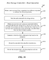
- FIG. 14 illustrates selected and exemplary instructions of the machine-readable, computer-readable or processing circuit-readable medium 1206 for use with a host storage controller such as the host storage controller 1301 of the processing circuit 1204 of FIG. 12 .
- the figure also illustrates selected and exemplary instructions of a machine-readable, computer-readable or processing circuit-readable medium 1401 for use with a storage device such as device 1205 of FIG. 12 .
- the machine-readable medium 1206 of FIG. 14 includes various instructions, which when executed by the host storage controller 1301 of FIG. 12 , cause the host storage controller to control or perform inline encryption/decryption operations.
- read/write command input instructions 1400 are operative to cause the host storage controller to obtain write commands from a requesting host software component (not shown in the figure) to write data to the storage device and also instructions operative to cause the host storage controller to obtain read commands from the requesting host software component to read data from the storage device.
- the machine-readable medium 1206 also includes: read/write command output instructions 1402 operative to cause the host storage controller to send read and write commands to the storage device 1205 and LBA/block count parameter input instructions 1404 operative to cause the host storage controller to obtain one or more parameters associated data to be read/written to/from the storage device such as an LBA and a block count.
- the machine-readable medium 1206 also includes: inline encryption instructions 1406 operative to cause the host storage controller to encrypt data using a host storage controller for storage in the storage device and inline decryption instructions 1408 operative to cause the host storage controller to decrypt data received from storage device. Still further the machine-readable medium 1206 includes: key processing instructions operative to cause the host storage controller to obtain or otherwise generate encryption/decryption keys based, at least in part, on the LBA or other parameters obtained by execution of the parameter input instructions 1404 .
- the machine-readable medium 1401 of FIG. 14 for use with the storage device of FIG. 12 includes read/write command input instructions 1412 , which when executed by the circuitry of the storage device, cause the storage device to receive read and/or write commands from the host storage controller 1301 of FIG. 12 indicating encrypted data to be read/written.
- LBA/block count parameter output instructions 1414 are operative to cause the storage device to output one or more parameters associated with data to be read/written such as the LBA and the block count to facilitate inline encryption/decryption of data within the host storage controller.
- the machine-readable medium 1401 also includes encrypted data input/output instructions operative to cause the storage device to receive encrypted data from the host storage controller (in conjunction with a write command) and to output encrypted data to the host storage controller (in conjunction with a read command.)
- An encrypted data storage unit 1418 stores the encrypted data.
- FIG. 15 broadly illustrates and summarizes methods or procedures 1500 that may be performed by the host storage controller 1301 of the processing circuit 1204 of FIG. 12 or other suitably equipped devices for inline encryption of data during a write operation.
- the host storage controller obtains a write command from a requesting host software component to write data to the storage device.
- the host storage controller sends the write command to the storage device.
- the host storage controller obtains a parameter associated with the data from the storage device wherein, in at least some examples, the parameter provides an identifier that is the same for read and write operations for a particular block of data but differs from one block of data to another.
- the host storage controller generates or otherwise obtains an encryption key based on the parameter and, at step 1510 , encrypts the data using the encryption key.
- the host storage controller sends the encrypted data to the storage device.
- FIG. 16 broadly illustrates and summarizes methods or procedures 1600 that may be performed by the host storage controller 1301 of the processing circuit 1204 of FIG. 12 or other suitably equipped devices for inline decryption of data during a read operation.
- the host storage controller obtains a read command from a requesting host software component to read data from the storage device.
- the host storage controller sends the read command to the storage device.
- the host storage controller obtains encrypted data and a parameter associated with the encrypted data from the storage device wherein, in at least some examples, the parameter provides an identifier that is the same for read and write operations for a particular block of data but differs from one block of data to another.
- the host storage controller generates or otherwise obtains a decryption key based on the parameter and, at step 1610 , decrypts the encrypted data using the decryption key.
- the host storage controller provides or “sends” the decrypted data to the requesting host software component.
- FIG. 17 broadly illustrates and summarizes methods or procedures 1700 that may be performed by the storage device 1205 of FIG. 12 or other suitably equipped devices for receiving and storing encrypted data from a host storage controller as part of a write operation.
- the storage device receives a write command from a host software controller indicating data to be written to the storage device.
- the host storage device sends a parameter associated with the data to the host storage controller to facilitate in-line encryption of the data by the host storage controller wherein, in at least some examples, the parameter provides an identifier that is the same for read and write operations for a particular block of data but differs from one block of data to another.
- the storage device receives the in-line encrypted data from the host storage controller and, at step 1708 , stores the in-line encrypted data received from the host storage controller.
- FIG. 18 broadly illustrates and summarizes methods or procedures 1800 that may be performed by the storage device 1205 of FIG. 12 or other suitably equipped devices for retrieving and sending encrypted data to a host storage controller as part of a read operation.
- the storage device receives a read command from a host software controller indicating encrypted data to be read from the storage device.
- the host storage retrieves the encrypted data.
- the storage device sends the encrypted data to the host storage controller along with a parameter associated with the encrypted data to facilitate in-line decryption of the data by the host storage controller wherein, in at least some examples, the parameter provides an identifier that is the same for read and write operations for a particular block of data but differs from one block of data to another.
- FIG. 19 broadly illustrates and summarizes alternative methods or procedures 1900 that may be performed by the host storage controller 1301 of the processing circuit 1204 of FIG. 12 or other suitably equipped devices for inline encryption of data during a write operation for use in implementations wherein the host storage controller does not receive the aforementioned parameters from the storage device from which encryption keys are generated.
- the host storage controller obtains a write command from a requesting host software component to write data to the storage device.
- the host storage controller sends the write command to the storage device.
- the host storage controller obtains a parameter from host memory wherein the parameter provides an identifier that is the same for read and write operations for a particular block of data but differs from one block of data to another.
- the host storage controller generates or otherwise obtains an encryption key based on the parameter and, at step 1910 , encrypts the data using the encryption key.
- the host storage controller sends the encrypted data to the storage device.
- FIG. 20 broadly illustrates and summarizes alternative methods or procedures 2000 that may be performed by the host storage controller 1301 of the processing circuit 1204 of FIG. 12 or other suitably equipped devices for inline decryption of data during a read operation for use in implementations wherein the host storage controller does not receive the aforementioned parameters from the storage device from which decryption keys are generated.
- the host storage controller obtains a read command from a requesting host software component to read data from the storage device.
- the host storage controller sends the read command to the storage device.
- the host storage controller obtains encrypted data from the storage device and also obtains a parameter from host memory wherein the parameter provides an identifier that is the same for read and write operations for a particular block of data but differs from one block of data to another.
- the host storage controller generates or otherwise obtains a decryption key based on the parameter and, at step 2010 , decrypts the encrypted data using the decryption key.
- the host storage controller provides or “sends” the decrypted data to the requesting host software component, typically by writing the data to host memory.
- a process is terminated when its operations are completed.
- a process may correspond to a method, a function, a procedure, a subroutine, a subprogram, etc.
- a process corresponds to a function
- its termination corresponds to a return of the function to the calling function or the main function.
- a software module may reside in RAM memory, flash memory, ROM memory, EPROM memory, EEPROM memory, registers, hard disk, a removable disk, a CD-ROM, or any other form of storage medium known in the art.
- a storage medium may be coupled to the processor such that the processor can read information from, and write information to, the storage medium. In the alternative, the storage medium may be integral to the processor.
Landscapes
- Engineering & Computer Science (AREA)
- Theoretical Computer Science (AREA)
- Physics & Mathematics (AREA)
- General Engineering & Computer Science (AREA)
- General Physics & Mathematics (AREA)
- Human Computer Interaction (AREA)
- Computer Security & Cryptography (AREA)
- Computer Hardware Design (AREA)
- Software Systems (AREA)
- Storage Device Security (AREA)
Priority Applications (6)
| Application Number | Priority Date | Filing Date | Title |
|---|---|---|---|
| US14/244,742 US20140310536A1 (en) | 2013-04-16 | 2014-04-03 | Storage device assisted inline encryption and decryption |
| PCT/US2014/033083 WO2014172124A1 (en) | 2013-04-16 | 2014-04-04 | Storage device assisted inline encryption and decryption |
| KR1020157032504A KR20150143708A (ko) | 2013-04-16 | 2014-04-04 | 스토리지 디바이스 보조 인라인 암호화 및 암호해독 |
| EP14724254.9A EP2987073A1 (en) | 2013-04-16 | 2014-04-04 | Storage device assisted inline encryption and decryption |
| JP2016508960A JP2016517241A (ja) | 2013-04-16 | 2014-04-04 | ストレージデバイスによって支援されるインライン暗号化および暗号化解除 |
| CN201480021176.3A CN105122203A (zh) | 2013-04-16 | 2014-04-04 | 存储设备辅助式内联加密和解密 |
Applications Claiming Priority (2)
| Application Number | Priority Date | Filing Date | Title |
|---|---|---|---|
| US201361812616P | 2013-04-16 | 2013-04-16 | |
| US14/244,742 US20140310536A1 (en) | 2013-04-16 | 2014-04-03 | Storage device assisted inline encryption and decryption |
Publications (1)
| Publication Number | Publication Date |
|---|---|
| US20140310536A1 true US20140310536A1 (en) | 2014-10-16 |
Family
ID=51687632
Family Applications (1)
| Application Number | Title | Priority Date | Filing Date |
|---|---|---|---|
| US14/244,742 Abandoned US20140310536A1 (en) | 2013-04-16 | 2014-04-03 | Storage device assisted inline encryption and decryption |
Country Status (6)
Cited By (41)
| Publication number | Priority date | Publication date | Assignee | Title |
|---|---|---|---|---|
| US20150074426A1 (en) * | 2013-09-10 | 2015-03-12 | Sebastien A. Jean | Generating and Using an Enhanced Initialization Vector |
| US20150242657A1 (en) * | 2014-02-27 | 2015-08-27 | Jisoo Kim | Self-encrypting drive and user device including the same |
| US20150278087A1 (en) * | 2014-03-26 | 2015-10-01 | Ilsu Han | Storage device and an operating method of the storage device |
| US20150371055A1 (en) * | 2014-06-19 | 2015-12-24 | Ju-hee Park | Host controller and system-on-chip |
| US20150372816A1 (en) * | 2014-06-19 | 2015-12-24 | Samsung Electronics Co., Ltd. | Semiconductor devices and methods of protecting data of channels in the same |
| US9225695B1 (en) | 2014-06-10 | 2015-12-29 | Lockheed Martin Corporation | Storing and transmitting sensitive data |
| WO2016072999A1 (en) * | 2014-11-07 | 2016-05-12 | Hewlett Packard Enterprise Development Lp | Data conversion using an address space identifier |
| US20160179702A1 (en) * | 2014-12-23 | 2016-06-23 | Siddhartha Chhabra | Memory Encryption Engine Integration |
| WO2017062242A1 (en) * | 2015-10-06 | 2017-04-13 | Micron Technology, Inc. | Secure subsystem |
| US9665501B1 (en) * | 2013-06-18 | 2017-05-30 | Western Digital Technologies, Inc. | Self-encrypting data storage device supporting object-level encryption |
| US20170185809A1 (en) * | 2014-12-23 | 2017-06-29 | Intel Corporation | Encryption Interface |
| US20180060741A1 (en) * | 2016-08-24 | 2018-03-01 | Fujitsu Limited | Medium storing data conversion program, data conversion device, and data conversion method |
| US9954681B2 (en) * | 2015-06-10 | 2018-04-24 | Nxp Usa, Inc. | Systems and methods for data encryption |
| US20180285575A1 (en) * | 2016-01-21 | 2018-10-04 | Hewlett-Packard Development Company, L.P. | Data cryptography engine |
| TWI645298B (zh) * | 2017-06-30 | 2018-12-21 | 慧榮科技股份有限公司 | 降低快閃儲存介面中傳收資料錯誤方法以及使用該方法的裝置 |
| US10169616B1 (en) * | 2016-02-01 | 2019-01-01 | Xilinx, Inc. | Cryptographic processing of data and instructions stored off-chip |
| WO2019035700A1 (en) * | 2017-08-18 | 2019-02-21 | Samsung Electronics Co., Ltd. | METHOD AND APPARATUS FOR BOARDING IN AN IOT NETWORK |
| US10298553B2 (en) | 2017-03-31 | 2019-05-21 | Sprint Communications Company L.P. | Hardware trusted data communications over system-on-chip (SOC) architectures |
| US10430789B1 (en) | 2014-06-10 | 2019-10-01 | Lockheed Martin Corporation | System, method and computer program product for secure retail transactions (SRT) |
| US10558393B2 (en) | 2017-10-20 | 2020-02-11 | Qualcomm Incorporated | Controller hardware automation for host-aware performance booster |
| US10599591B2 (en) | 2017-07-31 | 2020-03-24 | Samsung Electronics Co., Ltd. | Storage device for interfacing with host and method of operating the host and the storage device |
| US10630424B2 (en) | 2017-06-30 | 2020-04-21 | Silicon Motion, Inc. | Methods for reducing data errors in transceiving of a flash storage interface and apparatuses using the same |
| US10630425B2 (en) | 2017-06-30 | 2020-04-21 | Silicon Motion, Inc. | Methods for reducing data errors in transceiving of a flash storage interface and apparatuses using the same |
| US10637509B2 (en) | 2017-06-30 | 2020-04-28 | Silicon Motion, Inc. | Methods for reducing data errors in transceiving of a flash storage interface and apparatuses using the same |
| US10692335B2 (en) * | 2014-08-11 | 2020-06-23 | Seagate Technology Llc | Green drive with status indicator |
| US10848263B2 (en) | 2017-06-30 | 2020-11-24 | Silicon Motion, Inc. | Methods for reducing data errors in transceiving of a flash storage interface and apparatuses using the same |
| US10896267B2 (en) | 2017-01-31 | 2021-01-19 | Hewlett Packard Enterprise Development Lp | Input/output data encryption |
| US10969960B2 (en) | 2016-09-01 | 2021-04-06 | Samsung Electronics Co., Ltd. | Storage device and host for the same |
| US20210319121A1 (en) * | 2021-06-25 | 2021-10-14 | Intel Corporation | Concurrent volume and file based inline encryption on commodity operating systems |
| US20220027520A1 (en) * | 2020-07-24 | 2022-01-27 | Qualcomm Incorporated | Methods And Apparatus For In-Memory Device Access Control |
| US11349639B2 (en) * | 2018-12-28 | 2022-05-31 | ePIC Blockchain Technologies Inc. | Circuit and method for overcoming memory bottleneck of ASIC-resistant cryptographic algorithms |
| US11429751B2 (en) | 2019-07-01 | 2022-08-30 | Rajant Corporation | Method and apparatus for encrypting and decrypting data on an integrated circuit |
| US20220284110A1 (en) * | 2021-03-03 | 2022-09-08 | International Business Machines Corporation | Multi-key secure deduplication using locked fingerprints |
| US11494498B2 (en) * | 2014-07-03 | 2022-11-08 | Pure Storage, Inc. | Storage data decryption |
| US11797531B2 (en) * | 2020-08-04 | 2023-10-24 | Micron Technology, Inc. | Acceleration of data queries in memory |
| US20230350603A1 (en) * | 2022-04-28 | 2023-11-02 | Rambus Inc. | Securing dynamic random access memory (dram) contents to non-volatile in a persistent memory module |
| US20230409277A1 (en) * | 2022-06-21 | 2023-12-21 | Google Llc | Encrypting and/or decrypting audio data utilizing speaker features |
| US11941131B1 (en) * | 2020-12-31 | 2024-03-26 | Meta Platforms Technologies, Llc | Isolation of secrets from an operating system |
| US12001676B2 (en) | 2016-09-01 | 2024-06-04 | Samsung Electronics Co., Ltd. | Storage device and host for the same |
| TWI860846B (zh) * | 2023-09-21 | 2024-11-01 | 慧榮科技股份有限公司 | 電子裝置及耦接於記憶裝置的主裝置 |
| US12407495B2 (en) | 2020-09-14 | 2025-09-02 | Hewlett Packard Enterprise Development Lp | Encryption keys from storage systems |
Families Citing this family (9)
| Publication number | Priority date | Publication date | Assignee | Title |
|---|---|---|---|---|
| US10157153B2 (en) * | 2016-02-03 | 2018-12-18 | Qualcomm Incorporated | Inline cryptographic engine (ICE) for peripheral component interconnect express (PCIe) systems |
| KR102419505B1 (ko) * | 2016-03-09 | 2022-07-08 | 삼성전자주식회사 | 스토리지 디바이스의 인증 방법 및 시스템 |
| US20170372085A1 (en) * | 2016-06-28 | 2017-12-28 | HGST Netherlands B.V. | Protecting data in a storage device |
| US10476846B2 (en) * | 2016-08-05 | 2019-11-12 | The Boeing Company | Data-at-rest (DAR) encryption for integrated storage media |
| CN107332670A (zh) * | 2017-08-11 | 2017-11-07 | 北京中天信安科技有限责任公司 | 基于ufs接口的安全控制装置、系统、方法和移动设备 |
| KR20210016938A (ko) | 2019-08-06 | 2021-02-17 | 에스케이하이닉스 주식회사 | 데이터 처리 시스템 및 그것의 동작방법 |
| US11196846B2 (en) * | 2019-11-15 | 2021-12-07 | Facebook Technologies, Llc | Inline encryption of packet data in a wireless communication system |
| US11249924B2 (en) * | 2019-11-25 | 2022-02-15 | Micron Technology, Inc. | Secure data communication with memory sub-system |
| CN116881934B (zh) * | 2023-06-05 | 2024-02-23 | 珠海妙存科技有限公司 | 一种数据的加解密方法、系统、装置及存储介质 |
Citations (16)
| Publication number | Priority date | Publication date | Assignee | Title |
|---|---|---|---|---|
| US6449701B1 (en) * | 2000-09-20 | 2002-09-10 | Broadcom Corporation | Out of order associative queue in two clock domains |
| US20030065933A1 (en) * | 2001-09-28 | 2003-04-03 | Kabushiki Kaisha Toshiba | Microprocessor with improved task management and table management mechanism |
| US20050120260A1 (en) * | 2003-11-19 | 2005-06-02 | Fuji Xerox Co., Ltd | Image forming apparatus and control method of an image forming apparatus |
| US20050193103A1 (en) * | 2002-06-18 | 2005-09-01 | John Drabik | Method and apparatus for automatic configuration and management of a virtual private network |
| US20070116290A1 (en) * | 2005-11-10 | 2007-05-24 | Chih-Hao Yeh | Method of detecting incorrect IEEE 802.11 WEP key information entered in a wireless station |
| US20080052539A1 (en) * | 2006-07-29 | 2008-02-28 | Macmillan David M | Inline storage protection and key devices |
| US20080072071A1 (en) * | 2006-09-14 | 2008-03-20 | Seagate Technology Llc | Hard disc streaming cryptographic operations with embedded authentication |
| US20080273697A1 (en) * | 2007-05-01 | 2008-11-06 | Greco Paul M | Use of Indirect Data Keys for Encrypted Tape Cartridges |
| US20090187771A1 (en) * | 2008-01-17 | 2009-07-23 | Mclellan Jr Hubert Rae | Secure data storage with key update to prevent replay attacks |
| US7650510B2 (en) * | 2002-04-30 | 2010-01-19 | General Dynamics Advanced Information Systems, Inc. | Method and apparatus for in-line serial data encryption |
| US20100023721A1 (en) * | 2008-07-23 | 2010-01-28 | Takafumi Ito | Memory system and host device |
| US20110055664A1 (en) * | 2009-09-01 | 2011-03-03 | Gregory Burd | Systems and methods for compressing data in non-volatile semiconductor memory drives |
| US20110276802A1 (en) * | 2010-05-10 | 2011-11-10 | Qualcomm Incorporated | Methods and apparatus for peer-to-peer transfer of secure data using near field communications |
| US20120054570A1 (en) * | 2010-08-30 | 2012-03-01 | Hamilton Sundstrand Corporation | System for handling of permanent bit errors in memory devices |
| US8296584B2 (en) * | 2007-12-28 | 2012-10-23 | Alcatel Lucent | Storage and retrieval of encrypted data blocks with in-line message authentication codes |
| US20140289463A1 (en) * | 2013-03-20 | 2014-09-25 | Amazon Technologies, Inc. | Replication target service |
Family Cites Families (15)
| Publication number | Priority date | Publication date | Assignee | Title |
|---|---|---|---|---|
| US5058164A (en) * | 1990-05-03 | 1991-10-15 | National Semiconductor Corp. | Encryption of streams of addressed information to be used for program code protection |
| JP2005130059A (ja) * | 2003-10-22 | 2005-05-19 | Fuji Xerox Co Ltd | 画像形成装置および交換部品 |
| US7272727B2 (en) * | 2005-04-18 | 2007-09-18 | Hitachi, Ltd. | Method for managing external storage devices |
| JP4736593B2 (ja) * | 2005-07-25 | 2011-07-27 | ソニー株式会社 | データ記憶装置、データ記録方法、記録及び/又は再生システム、並びに、電子機器 |
| CN100561449C (zh) * | 2005-09-23 | 2009-11-18 | 中国科学院计算技术研究所 | 一种硬盘扇区级数据加密解密方法及系统 |
| US7443627B1 (en) * | 2006-03-07 | 2008-10-28 | Marvell International Ltd. | Lowest power mode for a mobile drive |
| JP2007336446A (ja) * | 2006-06-19 | 2007-12-27 | Canon Inc | データ暗号化装置 |
| US7953987B2 (en) * | 2007-03-06 | 2011-05-31 | International Business Machines Corporation | Protection of secure electronic modules against attacks |
| JP2010011247A (ja) * | 2008-06-30 | 2010-01-14 | Fujitsu Ltd | ディスク装置及び鍵交換方法 |
| CN101799789B (zh) * | 2009-02-05 | 2012-07-25 | 新唐科技股份有限公司 | 芯片及其存储器数据保护装置与其保护方法 |
| KR101601790B1 (ko) * | 2009-09-22 | 2016-03-21 | 삼성전자주식회사 | 암호키 선택장치를 구비하는 스토리지 시스템 및 암호 키 선택방법 |
| US8990582B2 (en) * | 2010-05-27 | 2015-03-24 | Cisco Technology, Inc. | Virtual machine memory compartmentalization in multi-core architectures |
| JP5521926B2 (ja) * | 2010-09-13 | 2014-06-18 | 富士通株式会社 | 記憶システム、制御装置、および記憶装置 |
| GB2489405B (en) * | 2011-03-22 | 2018-03-07 | Advanced Risc Mach Ltd | Encrypting and storing confidential data |
| JP5677336B2 (ja) * | 2011-08-01 | 2015-02-25 | 株式会社東芝 | メモリ・デバイス |
-
2014
- 2014-04-03 US US14/244,742 patent/US20140310536A1/en not_active Abandoned
- 2014-04-04 WO PCT/US2014/033083 patent/WO2014172124A1/en active Application Filing
- 2014-04-04 CN CN201480021176.3A patent/CN105122203A/zh active Pending
- 2014-04-04 KR KR1020157032504A patent/KR20150143708A/ko not_active Withdrawn
- 2014-04-04 EP EP14724254.9A patent/EP2987073A1/en not_active Withdrawn
- 2014-04-04 JP JP2016508960A patent/JP2016517241A/ja not_active Ceased
Patent Citations (16)
| Publication number | Priority date | Publication date | Assignee | Title |
|---|---|---|---|---|
| US6449701B1 (en) * | 2000-09-20 | 2002-09-10 | Broadcom Corporation | Out of order associative queue in two clock domains |
| US20030065933A1 (en) * | 2001-09-28 | 2003-04-03 | Kabushiki Kaisha Toshiba | Microprocessor with improved task management and table management mechanism |
| US7650510B2 (en) * | 2002-04-30 | 2010-01-19 | General Dynamics Advanced Information Systems, Inc. | Method and apparatus for in-line serial data encryption |
| US20050193103A1 (en) * | 2002-06-18 | 2005-09-01 | John Drabik | Method and apparatus for automatic configuration and management of a virtual private network |
| US20050120260A1 (en) * | 2003-11-19 | 2005-06-02 | Fuji Xerox Co., Ltd | Image forming apparatus and control method of an image forming apparatus |
| US20070116290A1 (en) * | 2005-11-10 | 2007-05-24 | Chih-Hao Yeh | Method of detecting incorrect IEEE 802.11 WEP key information entered in a wireless station |
| US20080052539A1 (en) * | 2006-07-29 | 2008-02-28 | Macmillan David M | Inline storage protection and key devices |
| US20080072071A1 (en) * | 2006-09-14 | 2008-03-20 | Seagate Technology Llc | Hard disc streaming cryptographic operations with embedded authentication |
| US20080273697A1 (en) * | 2007-05-01 | 2008-11-06 | Greco Paul M | Use of Indirect Data Keys for Encrypted Tape Cartridges |
| US8296584B2 (en) * | 2007-12-28 | 2012-10-23 | Alcatel Lucent | Storage and retrieval of encrypted data blocks with in-line message authentication codes |
| US20090187771A1 (en) * | 2008-01-17 | 2009-07-23 | Mclellan Jr Hubert Rae | Secure data storage with key update to prevent replay attacks |
| US20100023721A1 (en) * | 2008-07-23 | 2010-01-28 | Takafumi Ito | Memory system and host device |
| US20110055664A1 (en) * | 2009-09-01 | 2011-03-03 | Gregory Burd | Systems and methods for compressing data in non-volatile semiconductor memory drives |
| US20110276802A1 (en) * | 2010-05-10 | 2011-11-10 | Qualcomm Incorporated | Methods and apparatus for peer-to-peer transfer of secure data using near field communications |
| US20120054570A1 (en) * | 2010-08-30 | 2012-03-01 | Hamilton Sundstrand Corporation | System for handling of permanent bit errors in memory devices |
| US20140289463A1 (en) * | 2013-03-20 | 2014-09-25 | Amazon Technologies, Inc. | Replication target service |
Non-Patent Citations (3)
| Title |
|---|
| JEDEC Standard JESD220A June 2012 * |
| JEDEC Standard JESD220A June 2012 âââââ * |
| JEDEC Standard JESD223A June 2012 * |
Cited By (66)
| Publication number | Priority date | Publication date | Assignee | Title |
|---|---|---|---|---|
| US9665501B1 (en) * | 2013-06-18 | 2017-05-30 | Western Digital Technologies, Inc. | Self-encrypting data storage device supporting object-level encryption |
| US20150074426A1 (en) * | 2013-09-10 | 2015-03-12 | Sebastien A. Jean | Generating and Using an Enhanced Initialization Vector |
| US9959216B2 (en) * | 2013-09-10 | 2018-05-01 | Sandisk Technologies Llc | Generating and using an enhanced initialization vector |
| US20150242657A1 (en) * | 2014-02-27 | 2015-08-27 | Jisoo Kim | Self-encrypting drive and user device including the same |
| US20150278087A1 (en) * | 2014-03-26 | 2015-10-01 | Ilsu Han | Storage device and an operating method of the storage device |
| US9311506B1 (en) * | 2014-06-10 | 2016-04-12 | Lockheed Martin Corporation | Storing and transmitting sensitive data |
| US10430789B1 (en) | 2014-06-10 | 2019-10-01 | Lockheed Martin Corporation | System, method and computer program product for secure retail transactions (SRT) |
| US9419954B1 (en) | 2014-06-10 | 2016-08-16 | Lockheed Martin Corporation | Storing and transmitting sensitive data |
| US9225695B1 (en) | 2014-06-10 | 2015-12-29 | Lockheed Martin Corporation | Storing and transmitting sensitive data |
| US9760738B1 (en) | 2014-06-10 | 2017-09-12 | Lockheed Martin Corporation | Storing and transmitting sensitive data |
| US20150372816A1 (en) * | 2014-06-19 | 2015-12-24 | Samsung Electronics Co., Ltd. | Semiconductor devices and methods of protecting data of channels in the same |
| US10177913B2 (en) * | 2014-06-19 | 2019-01-08 | Samsung Electronics Co., Ltd. | Semiconductor devices and methods of protecting data of channels in the same |
| US20150371055A1 (en) * | 2014-06-19 | 2015-12-24 | Ju-hee Park | Host controller and system-on-chip |
| US9721113B2 (en) * | 2014-06-19 | 2017-08-01 | Samsung Electronics Co., Ltd. | Host controller and system-on-chip |
| US11494498B2 (en) * | 2014-07-03 | 2022-11-08 | Pure Storage, Inc. | Storage data decryption |
| US10692335B2 (en) * | 2014-08-11 | 2020-06-23 | Seagate Technology Llc | Green drive with status indicator |
| WO2016072999A1 (en) * | 2014-11-07 | 2016-05-12 | Hewlett Packard Enterprise Development Lp | Data conversion using an address space identifier |
| US9524249B2 (en) * | 2014-12-23 | 2016-12-20 | Intel Corporation | Memory encryption engine integration |
| US9910793B2 (en) * | 2014-12-23 | 2018-03-06 | Intel Corporation | Memory encryption engine integration |
| US11316661B2 (en) | 2014-12-23 | 2022-04-26 | Intel Corporation | Encryption interface |
| US20170185809A1 (en) * | 2014-12-23 | 2017-06-29 | Intel Corporation | Encryption Interface |
| US10530568B2 (en) * | 2014-12-23 | 2020-01-07 | Intel Corporation | Encryption interface |
| US12341870B2 (en) | 2014-12-23 | 2025-06-24 | Intel Corporation | Encryption interface |
| US20160179702A1 (en) * | 2014-12-23 | 2016-06-23 | Siddhartha Chhabra | Memory Encryption Engine Integration |
| US9954681B2 (en) * | 2015-06-10 | 2018-04-24 | Nxp Usa, Inc. | Systems and methods for data encryption |
| US10503934B2 (en) | 2015-10-06 | 2019-12-10 | Micron Technology, Inc. | Secure subsystem |
| WO2017062242A1 (en) * | 2015-10-06 | 2017-04-13 | Micron Technology, Inc. | Secure subsystem |
| US10068109B2 (en) | 2015-10-06 | 2018-09-04 | Micron Technology, Inc. | Secure subsystem |
| US9864879B2 (en) | 2015-10-06 | 2018-01-09 | Micron Technology, Inc. | Secure subsystem |
| US20180285575A1 (en) * | 2016-01-21 | 2018-10-04 | Hewlett-Packard Development Company, L.P. | Data cryptography engine |
| US10169616B1 (en) * | 2016-02-01 | 2019-01-01 | Xilinx, Inc. | Cryptographic processing of data and instructions stored off-chip |
| US10459878B2 (en) * | 2016-08-24 | 2019-10-29 | Fujitsu Limited | Medium storing data conversion program, data conversion device, and data conversion method |
| US20180060741A1 (en) * | 2016-08-24 | 2018-03-01 | Fujitsu Limited | Medium storing data conversion program, data conversion device, and data conversion method |
| US12001676B2 (en) | 2016-09-01 | 2024-06-04 | Samsung Electronics Co., Ltd. | Storage device and host for the same |
| US11567663B2 (en) | 2016-09-01 | 2023-01-31 | Samsung Electronics Co., Ltd. | Storage device and host for the same |
| US10969960B2 (en) | 2016-09-01 | 2021-04-06 | Samsung Electronics Co., Ltd. | Storage device and host for the same |
| US10896267B2 (en) | 2017-01-31 | 2021-01-19 | Hewlett Packard Enterprise Development Lp | Input/output data encryption |
| US10749847B2 (en) | 2017-03-31 | 2020-08-18 | Sprint Communications Company L.P. | Hardware trusted data communications over system-on-chip (SOC) architectures |
| US10298553B2 (en) | 2017-03-31 | 2019-05-21 | Sprint Communications Company L.P. | Hardware trusted data communications over system-on-chip (SOC) architectures |
| US10630425B2 (en) | 2017-06-30 | 2020-04-21 | Silicon Motion, Inc. | Methods for reducing data errors in transceiving of a flash storage interface and apparatuses using the same |
| US10637509B2 (en) | 2017-06-30 | 2020-04-28 | Silicon Motion, Inc. | Methods for reducing data errors in transceiving of a flash storage interface and apparatuses using the same |
| TWI645298B (zh) * | 2017-06-30 | 2018-12-21 | 慧榮科技股份有限公司 | 降低快閃儲存介面中傳收資料錯誤方法以及使用該方法的裝置 |
| US10630424B2 (en) | 2017-06-30 | 2020-04-21 | Silicon Motion, Inc. | Methods for reducing data errors in transceiving of a flash storage interface and apparatuses using the same |
| US10848263B2 (en) | 2017-06-30 | 2020-11-24 | Silicon Motion, Inc. | Methods for reducing data errors in transceiving of a flash storage interface and apparatuses using the same |
| US11080217B2 (en) * | 2017-07-31 | 2021-08-03 | Samsung Electronics Co., Ltd. | Storage device for interfacing with host and method of operating the host and the storage device |
| US11775455B2 (en) | 2017-07-31 | 2023-10-03 | Samsung Electronics Co., Ltd. | Storage device for interfacing with host and method of operating the host and the storage device |
| US11573915B2 (en) | 2017-07-31 | 2023-02-07 | Samsung Electronics Co., Ltd. | Storage device for interfacing with host and method of operating the host and the storage device |
| US10599591B2 (en) | 2017-07-31 | 2020-03-24 | Samsung Electronics Co., Ltd. | Storage device for interfacing with host and method of operating the host and the storage device |
| US11558187B2 (en) | 2017-08-18 | 2023-01-17 | Samsung Electronics Co., Ltd. | Method and an apparatus for onboarding in an IoT network |
| WO2019035700A1 (en) * | 2017-08-18 | 2019-02-21 | Samsung Electronics Co., Ltd. | METHOD AND APPARATUS FOR BOARDING IN AN IOT NETWORK |
| US20190058586A1 (en) * | 2017-08-18 | 2019-02-21 | Samsung Electronics Co., Ltd. | METHOD AND AN APPARATUS FOR ONBOARDING IN AN IoT NETWORK |
| US10558393B2 (en) | 2017-10-20 | 2020-02-11 | Qualcomm Incorporated | Controller hardware automation for host-aware performance booster |
| US11706020B2 (en) | 2018-12-28 | 2023-07-18 | ePIC Blockchain Technologies Inc. | Circuit and method for overcoming memory bottleneck of ASIC-resistant cryptographic algorithms |
| US11349639B2 (en) * | 2018-12-28 | 2022-05-31 | ePIC Blockchain Technologies Inc. | Circuit and method for overcoming memory bottleneck of ASIC-resistant cryptographic algorithms |
| US11429751B2 (en) | 2019-07-01 | 2022-08-30 | Rajant Corporation | Method and apparatus for encrypting and decrypting data on an integrated circuit |
| US20220027520A1 (en) * | 2020-07-24 | 2022-01-27 | Qualcomm Incorporated | Methods And Apparatus For In-Memory Device Access Control |
| US11636231B2 (en) * | 2020-07-24 | 2023-04-25 | Qualcomm Incorporated | Methods and apparatus for in-memory device access control |
| US11797531B2 (en) * | 2020-08-04 | 2023-10-24 | Micron Technology, Inc. | Acceleration of data queries in memory |
| US12407495B2 (en) | 2020-09-14 | 2025-09-02 | Hewlett Packard Enterprise Development Lp | Encryption keys from storage systems |
| US11941131B1 (en) * | 2020-12-31 | 2024-03-26 | Meta Platforms Technologies, Llc | Isolation of secrets from an operating system |
| US20220284110A1 (en) * | 2021-03-03 | 2022-09-08 | International Business Machines Corporation | Multi-key secure deduplication using locked fingerprints |
| US20210319121A1 (en) * | 2021-06-25 | 2021-10-14 | Intel Corporation | Concurrent volume and file based inline encryption on commodity operating systems |
| US20230350603A1 (en) * | 2022-04-28 | 2023-11-02 | Rambus Inc. | Securing dynamic random access memory (dram) contents to non-volatile in a persistent memory module |
| US12327042B2 (en) * | 2022-04-28 | 2025-06-10 | Rambus Inc. | Securing dynamic random access memory (DRAM) contents to non-volatile in a persistent memory module |
| US20230409277A1 (en) * | 2022-06-21 | 2023-12-21 | Google Llc | Encrypting and/or decrypting audio data utilizing speaker features |
| TWI860846B (zh) * | 2023-09-21 | 2024-11-01 | 慧榮科技股份有限公司 | 電子裝置及耦接於記憶裝置的主裝置 |
Also Published As
| Publication number | Publication date |
|---|---|
| JP2016517241A (ja) | 2016-06-09 |
| WO2014172124A1 (en) | 2014-10-23 |
| CN105122203A (zh) | 2015-12-02 |
| KR20150143708A (ko) | 2015-12-23 |
| EP2987073A1 (en) | 2016-02-24 |
Similar Documents
| Publication | Publication Date | Title |
|---|---|---|
| US20140310536A1 (en) | Storage device assisted inline encryption and decryption | |
| US10810138B2 (en) | Enhanced storage encryption with total memory encryption (TME) and multi-key total memory encryption (MKTME) | |
| TWI715619B (zh) | 用於硬體強制單向密碼學的處理器、方法及系統 | |
| CN111201553B (zh) | 一种安全元件及相关设备 | |
| CN103793629B (zh) | 处理安全内容的片上系统和包括片上系统的移动装置 | |
| US20090259857A1 (en) | System and Method for Efficient Security Domain Translation and Data Transfer | |
| US10303880B2 (en) | Security device having indirect access to external non-volatile memory | |
| EP3320476B1 (en) | Separation of software modules by controlled encryption key management | |
| US9460312B2 (en) | Data integrity protection from rollback attacks for use with systems employing message authentication code tags | |
| JP2017091543A (ja) | マルチプロセッサによって共有されるメモリを含むマルチプロセッサシステム、及び該システムの動作方法 | |
| US20170286320A1 (en) | Avoiding redundant memory encryption in a cryptographic protection system | |
| EP3117558A1 (en) | Dynamic encryption keys for use with xts encryption systems employing reduced-round ciphers | |
| US20210073145A1 (en) | Securing data direct i/o for a secure accelerator interface | |
| EP3758276B1 (en) | Data processing method, circuit, terminal device storage medium | |
| EP4134845B1 (en) | Memory access method, system-on-chip, and electronic device | |
| CN106156632B (zh) | 安全装置及在其内提供安全服务至主机的方法、安全设备 | |
| US20240202340A1 (en) | Trusted access control for secure boot process for storage controllers or drivers | |
| TW202424794A (zh) | 使用聯機密碼學硬體組件支援附加密碼學演算法 | |
| CN111783166A (zh) | 一种加密型eMCP芯片结构及数据处理方法 |
Legal Events
| Date | Code | Title | Description |
|---|---|---|---|
| AS | Assignment |
Owner name: QUALCOMM INCORPORATED, CALIFORNIA Free format text: ASSIGNMENT OF ASSIGNORS INTEREST;ASSIGNOR:SHACHAM, ASSAF;REEL/FRAME:032872/0601 Effective date: 20140430 |
|
| STPP | Information on status: patent application and granting procedure in general |
Free format text: FINAL REJECTION MAILED |
|
| STCB | Information on status: application discontinuation |
Free format text: ABANDONED -- FAILURE TO RESPOND TO AN OFFICE ACTION |