US20120249608A1 - Driver circuit for a display device, and driver cell - Google Patents
Driver circuit for a display device, and driver cell Download PDFInfo
- Publication number
- US20120249608A1 US20120249608A1 US13/432,853 US201213432853A US2012249608A1 US 20120249608 A1 US20120249608 A1 US 20120249608A1 US 201213432853 A US201213432853 A US 201213432853A US 2012249608 A1 US2012249608 A1 US 2012249608A1
- Authority
- US
- United States
- Prior art keywords
- driver circuit
- family
- sections
- operational amplifier
- decoder
- Prior art date
- Legal status (The legal status is an assumption and is not a legal conclusion. Google has not performed a legal analysis and makes no representation as to the accuracy of the status listed.)
- Granted
Links
- 239000000758 substrate Substances 0.000 claims abstract description 19
- 238000006243 chemical reaction Methods 0.000 claims description 4
- 239000004065 semiconductor Substances 0.000 claims description 2
- 239000002184 metal Substances 0.000 description 13
- 230000000694 effects Effects 0.000 description 3
- 230000002411 adverse Effects 0.000 description 1
- 239000000284 extract Substances 0.000 description 1
- 239000004973 liquid crystal related substance Substances 0.000 description 1
- 230000001360 synchronised effect Effects 0.000 description 1
Images


Classifications
-
- G—PHYSICS
- G09—EDUCATION; CRYPTOGRAPHY; DISPLAY; ADVERTISING; SEALS
- G09G—ARRANGEMENTS OR CIRCUITS FOR CONTROL OF INDICATING DEVICES USING STATIC MEANS TO PRESENT VARIABLE INFORMATION
- G09G3/00—Control arrangements or circuits, of interest only in connection with visual indicators other than cathode-ray tubes
- G09G3/20—Control arrangements or circuits, of interest only in connection with visual indicators other than cathode-ray tubes for presentation of an assembly of a number of characters, e.g. a page, by composing the assembly by combination of individual elements arranged in a matrix no fixed position being assigned to or needed to be assigned to the individual characters or partial characters
-
- G—PHYSICS
- G09—EDUCATION; CRYPTOGRAPHY; DISPLAY; ADVERTISING; SEALS
- G09G—ARRANGEMENTS OR CIRCUITS FOR CONTROL OF INDICATING DEVICES USING STATIC MEANS TO PRESENT VARIABLE INFORMATION
- G09G2300/00—Aspects of the constitution of display devices
- G09G2300/04—Structural and physical details of display devices
- G09G2300/0421—Structural details of the set of electrodes
- G09G2300/0426—Layout of electrodes and connections
-
- G—PHYSICS
- G09—EDUCATION; CRYPTOGRAPHY; DISPLAY; ADVERTISING; SEALS
- G09G—ARRANGEMENTS OR CIRCUITS FOR CONTROL OF INDICATING DEVICES USING STATIC MEANS TO PRESENT VARIABLE INFORMATION
- G09G2310/00—Command of the display device
- G09G2310/02—Addressing, scanning or driving the display screen or processing steps related thereto
- G09G2310/0264—Details of driving circuits
- G09G2310/027—Details of drivers for data electrodes, the drivers handling digital grey scale data, e.g. use of D/A converters
-
- G—PHYSICS
- G09—EDUCATION; CRYPTOGRAPHY; DISPLAY; ADVERTISING; SEALS
- G09G—ARRANGEMENTS OR CIRCUITS FOR CONTROL OF INDICATING DEVICES USING STATIC MEANS TO PRESENT VARIABLE INFORMATION
- G09G2320/00—Control of display operating conditions
- G09G2320/02—Improving the quality of display appearance
- G09G2320/0223—Compensation for problems related to R-C delay and attenuation in electrodes of matrix panels, e.g. in gate electrodes or on-substrate video signal electrodes
-
- G—PHYSICS
- G09—EDUCATION; CRYPTOGRAPHY; DISPLAY; ADVERTISING; SEALS
- G09G—ARRANGEMENTS OR CIRCUITS FOR CONTROL OF INDICATING DEVICES USING STATIC MEANS TO PRESENT VARIABLE INFORMATION
- G09G2320/00—Control of display operating conditions
- G09G2320/02—Improving the quality of display appearance
- G09G2320/0233—Improving the luminance or brightness uniformity across the screen
-
- G—PHYSICS
- G09—EDUCATION; CRYPTOGRAPHY; DISPLAY; ADVERTISING; SEALS
- G09G—ARRANGEMENTS OR CIRCUITS FOR CONTROL OF INDICATING DEVICES USING STATIC MEANS TO PRESENT VARIABLE INFORMATION
- G09G3/00—Control arrangements or circuits, of interest only in connection with visual indicators other than cathode-ray tubes
- G09G3/20—Control arrangements or circuits, of interest only in connection with visual indicators other than cathode-ray tubes for presentation of an assembly of a number of characters, e.g. a page, by composing the assembly by combination of individual elements arranged in a matrix no fixed position being assigned to or needed to be assigned to the individual characters or partial characters
- G09G3/34—Control arrangements or circuits, of interest only in connection with visual indicators other than cathode-ray tubes for presentation of an assembly of a number of characters, e.g. a page, by composing the assembly by combination of individual elements arranged in a matrix no fixed position being assigned to or needed to be assigned to the individual characters or partial characters by control of light from an independent source
- G09G3/36—Control arrangements or circuits, of interest only in connection with visual indicators other than cathode-ray tubes for presentation of an assembly of a number of characters, e.g. a page, by composing the assembly by combination of individual elements arranged in a matrix no fixed position being assigned to or needed to be assigned to the individual characters or partial characters by control of light from an independent source using liquid crystals
- G09G3/3611—Control of matrices with row and column drivers
- G09G3/3685—Details of drivers for data electrodes
Definitions
- the present invention relates to a driver circuit and driver cell for a display device.
- a driver circuit for a display device is generally formed as an integrated circuit chip.
- the chip is sometimes referred to as a source driver because it is connected to the source terminals of transistors in the display panel of the display device.
- FIG. 1 shows a conventional source driver chip 10 .
- the chip includes logic circuits 11 , level shifters 13 , decoders 13 , operational amplifiers (OP-AMPs) 14 , output pads 15 , and one or more ladders 18 formed on a rectangular chip substrate 16 . Responsive to input of an image data signal, the logic circuits 11 , level shifters 13 , decoders 13 , and operational amplifiers 14 select voltages generated by the ladders 18 to generate voltage signals representing the gradation levels of pixels in the image.
- OP-AMPs operational amplifiers
- the logic circuits 11 , level shifters 13 , decoders 13 , and operational amplifiers 14 are conventionally laid out in the order shown, with the logic circuits 11 near one long side 16 A of the chip substrate 16 and the operational amplifiers 14 near the opposite long side 16 B.
- the output pads 15 are formed on both long sides 16 A, 16 B of the substrate. Descriptions of driver circuits of this type can be found in, for example, Japanese Patent Application Publications No. 2009-59957 and 2009-253374.
- FIG. 2 shows an enlarged view of a conventional driver circuit, showing the part encircled by the dotted line X in FIG. 1 .
- the logic circuit 11 , level shifter 12 , decoder 13 , and operational amplifier 14 for one channel constitute a driver cell.
- the arrows in FIG. 2 indicate the flow of input data through the driver cells.
- the driver cells for two channels are normally formed as a single circuit group.
- FIG. 2 shows two such circuit groups A and B.
- the output pads 15 of adjacent circuit groups are disposed on opposite sides of the chip substrate 16 .
- the output pads 15 of circuit group A are on side 16 A and the output pads 15 of circuit group B are on side 16 B.
- the operational amplifiers 14 are connected to the output pads 15 by metal wiring patterns 17 A, 17 B.
- Metal wiring patterns 17 B extend from the operational amplifiers 14 in circuit group B to output pads 15 on the adjacent side 16 B, but metal wiring patterns 17 A must make lengthy detours around circuits 11 - 14 to reach the output pads 15 on the opposite side 16 A.
- a problem with the arrangement shown in FIG. 2 is that since the length of the metal wiring patterns connecting the operational amplifiers to the output pads differs from channel to channel, the output characteristics of the channels are non-uniform.
- a particular problem is that the wiring resistance in the long metal wiring patterns 17 A adversely affects the slew rate of the signals output from circuit group A.
- An object of the present invention is to reduce channel-to-channel variations in the output characteristics of a driver circuit for a display device.
- Another object is to improve the slew rate of the output signals of the driver circuit.
- the invention provides a novel driver circuit for receiving input image data and generating a plurality of drive signals for a display panel.
- the driver circuit is formed on a substrate and is organized into a plurality of sections. Each section includes a logic circuit for obtaining a digital value from the input image data and outputting a corresponding first digital signal, a level shifter for performing a level conversion operation on the first digital signal to obtain a second digital signal, a decoder for decoding the second digital signal to obtain a first voltage signal representing a pixel intensity gradation, an operational amplifier for converting the first voltage signal to a second voltage signal representing the pixel intensity gradation, and an output pad for output of the second voltage signal.
- the second voltage signal has a lower output impedance than the first voltage signal.
- the plurality of sections includes a first family of sections and a second family of sections.
- first family each section is laid out in a first spatial sequence in a first direction on the substrate.
- the first spatial sequence begins with the logic circuit, continues sequentially through the level shifter, the decoder, and the operational amplifier, and ends with the output pad.
- second family each section is laid out in a second spatial sequence in the first direction.
- the second spatial sequence begins with the output pad, continues sequentially through the operational amplifier, the logic circuit, and the level shifter, and ends with the decoder. At least one section in the first family and at least one section in the second family are mutually adjacent.
- each operational amplifier is connected to a spatially adjacent output pad.
- the driver circuit can therefore be designed so that all of the metal interconnection patterns are of substantially the same length, reducing channel-to-channel variations in the output characteristics, and all of the metal interconnection patterns are short, improving the slew rate of the output signals.
- the invention also provides a novel driver cell including a logic circuit, a level shifter, a decoder, and an operational amplifier as described above.
- the logic circuit, level shifter, and decoder occupy respective rectangular areas of a first width.
- the operational amplifier occupies a rectangular area of a second width greater than the first width.
- the novel driver cell provides extra space for the large output transistors in the operational amplifier and permits a space efficient layout of driver cells.
- FIG. 1 shows the circuit layout of a conventional driver circuit chip for a display device
- FIG. 2 shows an enlarged view of part X in FIG. 1 ;
- FIG. 3 shows the circuit layout of a novel driver circuit chip for a display device
- FIG. 4 shows an enlarged view of part Y in FIG. 3 ;
- FIG. 5 shows a variation of the internal data paths in FIG. 4 ;
- FIG. 6 shows another variation of the internal data paths in FIG. 4 .
- FIGS. 3 to 6 Novel driver circuits will now be described with reference to FIGS. 3 to 6 , in which like elements are indicated by like reference characters.
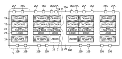
- an exemplary novel driver circuit includes logic circuits 21 , level shifters 23 , decoders 23 , operational amplifiers 24 , and output pads 25 A, 25 B formed on a rectangular semiconductor chip substrate 26 having two long sides 26 A, 26 B. Output pads 25 A are disposed on the first long side 26 A. Output pads 25 B are disposed on the second long side 26 B.
- a difference between this driver circuit and the conventional driver circuit 10 in FIG. 1 is that the operational amplifiers 24 are formed adjacent both long sides 26 A, 26 B.
- the driver circuit also includes ladders 28 that supply selectable voltage signals representing possible pixel gradations on the display panel (not shown) driven by the driver circuit.
- the display panel may be, for example, a liquid crystal display panel.
- Each ladder 28 may be configured as a series of resistors that divide a supplied voltage to generate the gradation voltages.
- driver chip logic circuits, level shifters, decoders, operational amplifiers, output pads
- driver chip logic circuits, level shifters, decoders, operational amplifiers, output pads
- the part of the driver circuit enclosed in the dotted line Y including four driver cells and their output pads, as shown in more detail in FIG. 4 .
- the first driver cell includes logic circuit 21 A, level shifter 22 A, decoder 23 A, and operational amplifier 24 A.
- Operational amplifier 24 A is disposed between decoder 23 A and an output pad 25 A on long side 26 A, and is connected to this output pad 25 A.
- the layout sequence, proceeding in the vertically upward direction in the drawing, begins with logic circuit 21 A, continues sequentially through level shifter 22 A, decoder 23 A, and operational amplifier 24 A, and ends with the output pad 25 A.
- the second driver cell includes logic circuit 21 B, level shifter 22 B, decoder 23 B, and operational amplifier 24 B.
- Operational amplifier 24 A is disposed between logic circuit 21 B and an output pad 25 B on long side 26 B, and is connected to this output pad 25 B.
- the layout sequence, proceeding in the vertically upward direction in the drawing, begins with the output pad 25 B, continues sequentially through operational amplifier 24 B, logic circuit 21 B, and level shifter 22 B, and ends with decoder 23 B.
- the other driver cells have similar layouts, cells in which the operational amplifier is adjacent side 26 A alternating with cells in which the operational amplifier is adjacent side 26 B.
- the logic circuit, level shifter, and decoder are laid out in mutually aligned rectangular areas of equal width.
- the operational amplifier occupies a rectangular area of twice this width.
- Each operational amplifier is aligned with the logic circuits, level shifters, and decoders in two mutually adjacent driver cells.
- Operational amplifier 24 A is connected to adjacent output pad 25 A by a metal wiring pattern 27 A.
- Operational amplifier 24 B is connected to adjacent output pad 25 B by a metal wiring pattern 27 B.
- These two metal wiring patterns 27 A, 27 B are both short and are of substantially equal length.
- the driver circuit can be divided into sections, each section including one driver cell and its connected output pad.
- the sections can be grouped into two families.
- the sections A 1 in the first family have operational amplifiers 24 A and output pads 25 A disposed adjacent side 26 A of the chip substrate 26 .
- the sections B 1 in the second family have operational amplifiers 24 B and output pads 25 B disposed adjacent side 26 B.
- the sections A 1 in the first family alternate with the sections B 1 in the second family in the horizontal direction in FIG. 4 .
- the logic circuits in all the driver cells are aligned in a single horizontal row.
- the level shifters in all the driver cells are aligned in a single horizontal row
- the decoders in all the driver cells are aligned in a single horizontal row.
- the logic circuits 21 A, 21 B obtain digital values (eight-bit signals, for example) from input image data.
- the input image data signal is synchronized with a clock signal and follows a route that, for example, passes first through the logic circuits 21 A in the first family of sections A 1 and then returns through the logic circuits 21 B in the second family of sections B 1 , as indicated by the horizontal arrows.
- Each logic circuit extracts the digital value representing one pixel of the image to be displayed, and outputs it as a digital signal.
- the level shifters 22 A, 22 B perform a voltage level conversion operation on each bit of the digital signals output by the logic circuits 21 A, 21 B and output the converted digital signals.
- the decoders 23 A, 23 B decode the converted digital signals in order to select corresponding voltage signals generated by the ladders 28 in FIG. 3 , and output corresponding voltage signals representing the gradation levels of pixels in the image to be displayed. These voltage signals have a comparatively high output impedance, suitable for the high input impedance of the operational amplifiers 24 A, 24 B.
- the operational amplifiers 24 A, 24 B convert the high-impedance voltage signals from the decoders to low-impedance signals that can be used to drive the display panel.
- the operation amplifiers 24 A, 24 B may be configured as voltage followers.
- the low-impedance voltage signals are output from the output pads 25 A, 25 B.
- the signal flow includes both an upward segment from the logic circuits 21 B to the decoders 23 B and a downward segment from the decoders 23 B to the operational amplifiers 24 B, as indicated by arrows SB.
- the voltage signals output by the decoders 23 B are routed straight through the level shifters 22 B and logic circuits 21 B in the same driver cell, without making detours outside the cell.
- the extra interconnection length between the decoders 23 B and operational amplifiers 24 B in the second family of sections B 1 has some effect on the output characteristics of the second family of sections B 1 .
- the high input impedance of the operational amplifiers 24 B and the lack of detours minimizes this effect, however, so it is much less than the effect of the conventional roundabout metal wiring patterns 17 A in FIG. 2 .
- One advantage of the circuit layout in FIG. 4 is that the short length of the metal wiring patterns connecting the operational amplifiers 24 A, 24 B to the output pads 25 A, 25 B improves the slew rate of the output voltage signals of the chip.
- Another advantage is that the substantially uniform length of the metal wiring patterns connecting the operational amplifiers 24 A, 24 B to the output pads 25 A, 25 B reduces channel-to-channel variations in the output characteristics of the chip.
- Another advantage is that the extra width allotted to the operational amplifiers 24 A, 24 B, which have comparatively large output transistors, enables space on the chip to be used efficiently, so that the size of the chip can be reduced.
- the lack of wiring detours also contributes to space efficiency and reduced chip size.
- FIG. 5 shows a variation of the layout in FIG. 4 in which two driver cells in the first family of sections A 1 are laid out side by side, and two driver cells in the second family of sections B 1 are laid out side by side. In the horizontal direction, pairs of sections A 1 in the first family alternate with pairs of sections B 1 in the second family.
- FIG. 6 shows another variation of the layout in FIG. 4 in which three driver cells in the first family of sections A 1 are laid out side by side, and three driver cells in the second family of sections B 1 are laid out side by side.
- triplets of sections A 1 in the first family alternate with triplets of section B 1 in the second family.
- N sections A 1 in the first family may alternate with N section B 1 in the second family, where N is any positive integer.
- novel circuit configuration shown in any of FIGS. 3 to 6 and the conventional circuit configuration shown in FIGS. 1 and 2 may both be used in the same driver chip.
- novel circuit configuration shown in any of FIGS. 3 to 6 may also be used in a driver circuit in which the logic circuits, level shifters, decoders, and operational amplifiers are separate integrated circuits and the substrate is a printed circuit board.
Landscapes
- Engineering & Computer Science (AREA)
- Physics & Mathematics (AREA)
- Computer Hardware Design (AREA)
- General Physics & Mathematics (AREA)
- Theoretical Computer Science (AREA)
- Control Of Indicators Other Than Cathode Ray Tubes (AREA)
- Liquid Crystal Display Device Control (AREA)
Abstract
Description
- 1. Field of the Invention
- The present invention relates to a driver circuit and driver cell for a display device.
- 2. Description of the Related Art
- A driver circuit for a display device is generally formed as an integrated circuit chip. The chip is sometimes referred to as a source driver because it is connected to the source terminals of transistors in the display panel of the display device.
-
FIG. 1 shows a conventionalsource driver chip 10. The chip includeslogic circuits 11,level shifters 13,decoders 13, operational amplifiers (OP-AMPs) 14,output pads 15, and one ormore ladders 18 formed on arectangular chip substrate 16. Responsive to input of an image data signal, thelogic circuits 11,level shifters 13,decoders 13, andoperational amplifiers 14 select voltages generated by theladders 18 to generate voltage signals representing the gradation levels of pixels in the image. - The
logic circuits 11,level shifters 13,decoders 13, andoperational amplifiers 14 are conventionally laid out in the order shown, with thelogic circuits 11 near onelong side 16A of thechip substrate 16 and theoperational amplifiers 14 near the oppositelong side 16B. Theoutput pads 15 are formed on bothlong sides -
FIG. 2 shows an enlarged view of a conventional driver circuit, showing the part encircled by the dotted line X inFIG. 1 . There is onelogic circuit 11, onelevel shifter 12, onedecoder 13, oneoperational amplifier 14, and oneoutput pad 15 for each column of pixels in the display panel. That is, there is one output signal channel for each column of pixels. Thelogic circuit 11,level shifter 12,decoder 13, andoperational amplifier 14 for one channel constitute a driver cell. The arrows inFIG. 2 indicate the flow of input data through the driver cells. - The driver cells for two channels are normally formed as a single circuit group.
FIG. 2 shows two such circuit groups A and B. Theoutput pads 15 of adjacent circuit groups are disposed on opposite sides of thechip substrate 16. InFIG. 2 theoutput pads 15 of circuit group A are onside 16A and theoutput pads 15 of circuit group B are onside 16B. - The
operational amplifiers 14 are connected to theoutput pads 15 bymetal wiring patterns 17A, 17B.Metal wiring patterns 17B extend from theoperational amplifiers 14 in circuit group B tooutput pads 15 on theadjacent side 16B, but metal wiring patterns 17A must make lengthy detours around circuits 11-14 to reach theoutput pads 15 on theopposite side 16A. - A problem with the arrangement shown in
FIG. 2 is that since the length of the metal wiring patterns connecting the operational amplifiers to the output pads differs from channel to channel, the output characteristics of the channels are non-uniform. A particular problem is that the wiring resistance in the long metal wiring patterns 17A adversely affects the slew rate of the signals output from circuit group A. - An object of the present invention is to reduce channel-to-channel variations in the output characteristics of a driver circuit for a display device.
- Another object is to improve the slew rate of the output signals of the driver circuit.
- The invention provides a novel driver circuit for receiving input image data and generating a plurality of drive signals for a display panel. The driver circuit is formed on a substrate and is organized into a plurality of sections. Each section includes a logic circuit for obtaining a digital value from the input image data and outputting a corresponding first digital signal, a level shifter for performing a level conversion operation on the first digital signal to obtain a second digital signal, a decoder for decoding the second digital signal to obtain a first voltage signal representing a pixel intensity gradation, an operational amplifier for converting the first voltage signal to a second voltage signal representing the pixel intensity gradation, and an output pad for output of the second voltage signal. The second voltage signal has a lower output impedance than the first voltage signal.
- The plurality of sections includes a first family of sections and a second family of sections. In the first family, each section is laid out in a first spatial sequence in a first direction on the substrate. The first spatial sequence begins with the logic circuit, continues sequentially through the level shifter, the decoder, and the operational amplifier, and ends with the output pad. In the second family, each section is laid out in a second spatial sequence in the first direction. The second spatial sequence begins with the output pad, continues sequentially through the operational amplifier, the logic circuit, and the level shifter, and ends with the decoder. At least one section in the first family and at least one section in the second family are mutually adjacent.
- In both sequences each operational amplifier is connected to a spatially adjacent output pad. The driver circuit can therefore be designed so that all of the metal interconnection patterns are of substantially the same length, reducing channel-to-channel variations in the output characteristics, and all of the metal interconnection patterns are short, improving the slew rate of the output signals.
- The invention also provides a novel driver cell including a logic circuit, a level shifter, a decoder, and an operational amplifier as described above. The logic circuit, level shifter, and decoder occupy respective rectangular areas of a first width. The operational amplifier occupies a rectangular area of a second width greater than the first width.
- The novel driver cell provides extra space for the large output transistors in the operational amplifier and permits a space efficient layout of driver cells.
- In the attached drawings:
-
FIG. 1 shows the circuit layout of a conventional driver circuit chip for a display device; -
FIG. 2 shows an enlarged view of part X inFIG. 1 ; -
FIG. 3 shows the circuit layout of a novel driver circuit chip for a display device; -
FIG. 4 shows an enlarged view of part Y inFIG. 3 ; -
FIG. 5 shows a variation of the internal data paths inFIG. 4 ; and -
FIG. 6 shows another variation of the internal data paths inFIG. 4 . - Novel driver circuits will now be described with reference to
FIGS. 3 to 6 , in which like elements are indicated by like reference characters. - Referring to
FIG. 3 , an exemplary novel driver circuit includeslogic circuits 21,level shifters 23,decoders 23,operational amplifiers 24, andoutput pads semiconductor chip substrate 26 having twolong sides Output pads 25A are disposed on the firstlong side 26A.Output pads 25B are disposed on the secondlong side 26B. A difference between this driver circuit and theconventional driver circuit 10 inFIG. 1 is that theoperational amplifiers 24 are formed adjacent bothlong sides - The driver circuit also includes
ladders 28 that supply selectable voltage signals representing possible pixel gradations on the display panel (not shown) driven by the driver circuit. The display panel may be, for example, a liquid crystal display panel. Eachladder 28 may be configured as a series of resistors that divide a supplied voltage to generate the gradation voltages. - Although the same terminology as in the background art is used herein to describe the components of the driver chip (logic circuits, level shifters, decoders, operational amplifiers, output pads), it will be appreciated that the same or equivalent circuit elements may be designated by different names, and that the invention is not limited to any particular terminology.
- The part of the driver circuit enclosed in the dotted line Y, including four driver cells and their output pads, as shown in more detail in
FIG. 4 . - The first driver cell includes
logic circuit 21A,level shifter 22A,decoder 23A, andoperational amplifier 24A.Operational amplifier 24A is disposed betweendecoder 23A and anoutput pad 25A onlong side 26A, and is connected to thisoutput pad 25A. The layout sequence, proceeding in the vertically upward direction in the drawing, begins withlogic circuit 21A, continues sequentially throughlevel shifter 22A,decoder 23A, andoperational amplifier 24A, and ends with theoutput pad 25A. - The second driver cell includes
logic circuit 21B,level shifter 22B,decoder 23B, andoperational amplifier 24B.Operational amplifier 24A is disposed betweenlogic circuit 21B and anoutput pad 25B onlong side 26B, and is connected to thisoutput pad 25B. The layout sequence, proceeding in the vertically upward direction in the drawing, begins with theoutput pad 25B, continues sequentially throughoperational amplifier 24B,logic circuit 21B, andlevel shifter 22B, and ends withdecoder 23B. - The other driver cells have similar layouts, cells in which the operational amplifier is
adjacent side 26A alternating with cells in which the operational amplifier isadjacent side 26B. In each cell, the logic circuit, level shifter, and decoder are laid out in mutually aligned rectangular areas of equal width. The operational amplifier occupies a rectangular area of twice this width. Each operational amplifier is aligned with the logic circuits, level shifters, and decoders in two mutually adjacent driver cells. -
Operational amplifier 24A is connected toadjacent output pad 25A by ametal wiring pattern 27A.Operational amplifier 24B is connected toadjacent output pad 25B by ametal wiring pattern 27B. These twometal wiring patterns - The driver circuit can be divided into sections, each section including one driver cell and its connected output pad. The sections can be grouped into two families. The sections A1 in the first family have
operational amplifiers 24A andoutput pads 25A disposedadjacent side 26A of thechip substrate 26. The sections B1 in the second family haveoperational amplifiers 24B andoutput pads 25B disposedadjacent side 26B. The sections A1 in the first family alternate with the sections B1 in the second family in the horizontal direction inFIG. 4 . The logic circuits in all the driver cells are aligned in a single horizontal row. Similarly, the level shifters in all the driver cells are aligned in a single horizontal row, and the decoders in all the driver cells are aligned in a single horizontal row. - The
logic circuits logic circuits 21A in the first family of sections A1 and then returns through thelogic circuits 21B in the second family of sections B1, as indicated by the horizontal arrows. Each logic circuit extracts the digital value representing one pixel of the image to be displayed, and outputs it as a digital signal. - The
level shifters logic circuits - The
decoders ladders 28 inFIG. 3 , and output corresponding voltage signals representing the gradation levels of pixels in the image to be displayed. These voltage signals have a comparatively high output impedance, suitable for the high input impedance of theoperational amplifiers - The
operational amplifiers operation amplifiers output pads - The signal flow from the
logic circuits 21A to theoperational amplifiers 24A in the first family of sections A1 is straight upward inFIG. 4 , as indicated by arrow SA. - In the second family of sections B1, however, the signal flow includes both an upward segment from the
logic circuits 21B to thedecoders 23B and a downward segment from thedecoders 23B to theoperational amplifiers 24B, as indicated by arrows SB. In the downward segment from thedecoders 23B to theoperational amplifiers 24B, the voltage signals output by thedecoders 23B are routed straight through thelevel shifters 22B andlogic circuits 21B in the same driver cell, without making detours outside the cell. - The extra interconnection length between the
decoders 23B andoperational amplifiers 24B in the second family of sections B1 has some effect on the output characteristics of the second family of sections B1. The high input impedance of theoperational amplifiers 24B and the lack of detours minimizes this effect, however, so it is much less than the effect of the conventional roundabout metal wiring patterns 17A inFIG. 2 . - One advantage of the circuit layout in
FIG. 4 is that the short length of the metal wiring patterns connecting theoperational amplifiers output pads - Another advantage is that the substantially uniform length of the metal wiring patterns connecting the
operational amplifiers output pads - Another advantage is that the extra width allotted to the
operational amplifiers -
FIG. 5 shows a variation of the layout inFIG. 4 in which two driver cells in the first family of sections A1 are laid out side by side, and two driver cells in the second family of sections B1 are laid out side by side. In the horizontal direction, pairs of sections A1 in the first family alternate with pairs of sections B1 in the second family. -
FIG. 6 shows another variation of the layout inFIG. 4 in which three driver cells in the first family of sections A1 are laid out side by side, and three driver cells in the second family of sections B1 are laid out side by side. In the horizontal direction, triplets of sections A1 in the first family alternate with triplets of section B1 in the second family. - In the general case, N sections A1 in the first family may alternate with N section B1 in the second family, where N is any positive integer.
- The novel circuit configuration shown in any of
FIGS. 3 to 6 and the conventional circuit configuration shown inFIGS. 1 and 2 may both be used in the same driver chip. - The novel circuit configuration shown in any of
FIGS. 3 to 6 may also be used in a driver circuit in which the logic circuits, level shifters, decoders, and operational amplifiers are separate integrated circuits and the substrate is a printed circuit board. - Those skilled in the art will recognize that further variations are possible within the scope of the invention, which is defined in the appended claims.
Claims (16)
Applications Claiming Priority (2)
| Application Number | Priority Date | Filing Date | Title |
|---|---|---|---|
| JP2011-078963 | 2011-03-31 | ||
| JP2011078963A JP5754845B2 (en) | 2011-03-31 | 2011-03-31 | Display device drive circuit and driver cell |
Publications (2)
| Publication Number | Publication Date |
|---|---|
| US20120249608A1 true US20120249608A1 (en) | 2012-10-04 |
| US9007292B2 US9007292B2 (en) | 2015-04-14 |
Family
ID=46926625
Family Applications (1)
| Application Number | Title | Priority Date | Filing Date |
|---|---|---|---|
| US13/432,853 Expired - Fee Related US9007292B2 (en) | 2011-03-31 | 2012-03-28 | Driver circuit and driver cell generating drive signal for display panel |
Country Status (3)
| Country | Link |
|---|---|
| US (1) | US9007292B2 (en) |
| JP (1) | JP5754845B2 (en) |
| CN (1) | CN102737573B (en) |
Cited By (4)
| Publication number | Priority date | Publication date | Assignee | Title |
|---|---|---|---|---|
| US20130181956A1 (en) * | 2012-01-13 | 2013-07-18 | Raydium Semiconductor Corporation | Driving apparatus |
| US20130181963A1 (en) * | 2012-01-13 | 2013-07-18 | Raydium Semiconductor Corporation | Driving apparatus |
| WO2020073872A1 (en) * | 2018-10-09 | 2020-04-16 | 京东方科技集团股份有限公司 | Microfluidic chip and driving method therefor |
| US11328683B2 (en) * | 2020-02-05 | 2022-05-10 | Lapis Semiconductor Co., Ltd. | Display device and source driver |
Citations (9)
| Publication number | Priority date | Publication date | Assignee | Title |
|---|---|---|---|---|
| US5523772A (en) * | 1993-05-07 | 1996-06-04 | Samsung Electronics Co., Ltd. | Source driving device of a liquid crystal display |
| US20040179027A1 (en) * | 2003-03-10 | 2004-09-16 | Nec Electronics Corporation | Drive circuit of display apparatus |
| US20050151714A1 (en) * | 2004-01-13 | 2005-07-14 | Atsushi Hirama | Output circuit, liquid crystal driving circuit, and liquid crystal driving method |
| US20050219195A1 (en) * | 2004-03-30 | 2005-10-06 | Takeshi Yano | Display device and driving device |
| US20060197734A1 (en) * | 2005-03-02 | 2006-09-07 | Seiko Epson Corporation | Reference voltage generation circuit, display driver, electro-optical device, and electronic instrument |
| US20070152947A1 (en) * | 2005-12-22 | 2007-07-05 | Yasuhiro Tanaka | Display apparatus |
| US20070195053A1 (en) * | 2006-02-23 | 2007-08-23 | Mitsubishi Electric Corporation | Shift register circuit and image display apparatus containing the same |
| US20070229440A1 (en) * | 2006-03-30 | 2007-10-04 | Chih-Jen Yen | Source driver of an lcd panel with reduced voltage buffers and method of driving the same |
| US20100013869A1 (en) * | 2008-07-17 | 2010-01-21 | Hitachi Displays, Ltd. | Display Device |
Family Cites Families (9)
| Publication number | Priority date | Publication date | Assignee | Title |
|---|---|---|---|---|
| JP3433337B2 (en) * | 1995-07-11 | 2003-08-04 | 日本テキサス・インスツルメンツ株式会社 | Signal line drive circuit for liquid crystal display |
| JP3417514B2 (en) * | 1996-04-09 | 2003-06-16 | 株式会社日立製作所 | Liquid crystal display |
| JP2003202846A (en) * | 2001-10-30 | 2003-07-18 | Sharp Corp | Display device and driving method thereof |
| JP3613240B2 (en) * | 2001-12-05 | 2005-01-26 | セイコーエプソン株式会社 | Display driving circuit, electro-optical device, and display driving method |
| KR100763847B1 (en) * | 2005-12-20 | 2007-10-05 | 삼성전자주식회사 | Driving integrated circuit of liquid crystal display device having double column structure |
| JP2009020511A (en) * | 2007-06-15 | 2009-01-29 | Toshiba Corp | Display control circuit |
| JP4540697B2 (en) | 2007-08-31 | 2010-09-08 | Okiセミコンダクタ株式会社 | Semiconductor device |
| JP5128996B2 (en) | 2008-04-01 | 2013-01-23 | ラピスセミコンダクタ株式会社 | Output circuit and offset canceling method |
| US20090284317A1 (en) * | 2008-05-16 | 2009-11-19 | Ching-Chung Lee | Source driver of a display, operational amplifier, and method for controlling the operational amplifier thereof |
-
2011
- 2011-03-31 JP JP2011078963A patent/JP5754845B2/en not_active Expired - Fee Related
-
2012
- 2012-03-28 US US13/432,853 patent/US9007292B2/en not_active Expired - Fee Related
- 2012-03-31 CN CN201210093696.8A patent/CN102737573B/en not_active Expired - Fee Related
Patent Citations (10)
| Publication number | Priority date | Publication date | Assignee | Title |
|---|---|---|---|---|
| US5523772A (en) * | 1993-05-07 | 1996-06-04 | Samsung Electronics Co., Ltd. | Source driving device of a liquid crystal display |
| US20040179027A1 (en) * | 2003-03-10 | 2004-09-16 | Nec Electronics Corporation | Drive circuit of display apparatus |
| US20050151714A1 (en) * | 2004-01-13 | 2005-07-14 | Atsushi Hirama | Output circuit, liquid crystal driving circuit, and liquid crystal driving method |
| US20050219195A1 (en) * | 2004-03-30 | 2005-10-06 | Takeshi Yano | Display device and driving device |
| US20060197734A1 (en) * | 2005-03-02 | 2006-09-07 | Seiko Epson Corporation | Reference voltage generation circuit, display driver, electro-optical device, and electronic instrument |
| US20070152947A1 (en) * | 2005-12-22 | 2007-07-05 | Yasuhiro Tanaka | Display apparatus |
| US20110007065A1 (en) * | 2005-12-22 | 2011-01-13 | Hitachi Displays, Ltd.. | Display apparatus |
| US20070195053A1 (en) * | 2006-02-23 | 2007-08-23 | Mitsubishi Electric Corporation | Shift register circuit and image display apparatus containing the same |
| US20070229440A1 (en) * | 2006-03-30 | 2007-10-04 | Chih-Jen Yen | Source driver of an lcd panel with reduced voltage buffers and method of driving the same |
| US20100013869A1 (en) * | 2008-07-17 | 2010-01-21 | Hitachi Displays, Ltd. | Display Device |
Cited By (7)
| Publication number | Priority date | Publication date | Assignee | Title |
|---|---|---|---|---|
| US20130181956A1 (en) * | 2012-01-13 | 2013-07-18 | Raydium Semiconductor Corporation | Driving apparatus |
| US20130181963A1 (en) * | 2012-01-13 | 2013-07-18 | Raydium Semiconductor Corporation | Driving apparatus |
| US8866721B2 (en) * | 2012-01-13 | 2014-10-21 | Raydium Semiconductor Corporation | Driving apparatus |
| US8866722B2 (en) * | 2012-01-13 | 2014-10-21 | Raydium Semiconductor Corporation | Driving apparatus |
| WO2020073872A1 (en) * | 2018-10-09 | 2020-04-16 | 京东方科技集团股份有限公司 | Microfluidic chip and driving method therefor |
| US11654433B2 (en) | 2018-10-09 | 2023-05-23 | Beijing Boe Optoelectronics Technology Co., Ltd. | Microfluidic chip and driving method thereof |
| US11328683B2 (en) * | 2020-02-05 | 2022-05-10 | Lapis Semiconductor Co., Ltd. | Display device and source driver |
Also Published As
| Publication number | Publication date |
|---|---|
| JP5754845B2 (en) | 2015-07-29 |
| JP2012215602A (en) | 2012-11-08 |
| CN102737573A (en) | 2012-10-17 |
| CN102737573B (en) | 2017-05-10 |
| US9007292B2 (en) | 2015-04-14 |
Similar Documents
| Publication | Publication Date | Title |
|---|---|---|
| US11423831B2 (en) | Driving method for a display device and a display device | |
| JP6272712B2 (en) | Drive device for display device | |
| US7902645B2 (en) | Semiconductor device, semiconductor element, and substrate | |
| KR101228654B1 (en) | Display device | |
| US9007292B2 (en) | Driver circuit and driver cell generating drive signal for display panel | |
| CN104637429B (en) | Display drive circuit and display device | |
| JP2020525807A (en) | Array substrate and display device | |
| US8154132B2 (en) | Semiconductor device comprising internal and external wiring | |
| CN101901803B (en) | Semiconductor device and data driver of display apparatus using the same | |
| WO2011048723A1 (en) | Display panel driving semiconductor integrated circuit, display panel driving module and display apparatus | |
| TWI796942B (en) | Driver integrated circuit | |
| TW201329943A (en) | Driving apparatus | |
| CN100442942C (en) | Array driving system and method for driving load | |
| JP4635020B2 (en) | Gradation voltage selection circuit and display control circuit | |
| CN103913915B (en) | A kind of array base palte, display floater and display device | |
| US8384642B2 (en) | Signal line driving device comprising a plurality of outputs | |
| JP2009020511A (en) | Display control circuit | |
| KR20060046349A (en) | Semiconductor integrated circuit device | |
| CN100476910C (en) | Flat display device and mobile terminal device | |
| EP2472313A1 (en) | Chip on glass type liquid crystal display | |
| KR102596604B1 (en) | Drive ic and display device using the same | |
| JP2000163018A (en) | Integrated circuit and liquid crystal display device using same | |
| CN110288955B (en) | Display drivers, electro-optical devices and electronic equipment | |
| JP2015143885A (en) | Drive circuit for display device | |
| JP5117817B2 (en) | Multi-level voltage generator, data driver, and liquid crystal display device |
Legal Events
| Date | Code | Title | Description |
|---|---|---|---|
| AS | Assignment |
Owner name: LAPIS SEMICONDUCTOR CO., LTD., JAPAN Free format text: ASSIGNMENT OF ASSIGNORS INTEREST;ASSIGNORS:IKARI, JUNKO;HASEGAWA, HIDEAKI;REEL/FRAME:027948/0665 Effective date: 20120127 |
|
| AS | Assignment |
Owner name: LAPIS SEMICONDUCTOR CO., LTD., JAPAN Free format text: CHANGE OF ADDRESS;ASSIGNOR:LAPIS SEMICONDUCTOR CO., LTD.,;REEL/FRAME:032495/0049 Effective date: 20130306 |
|
| STCF | Information on status: patent grant |
Free format text: PATENTED CASE |
|
| MAFP | Maintenance fee payment |
Free format text: PAYMENT OF MAINTENANCE FEE, 4TH YEAR, LARGE ENTITY (ORIGINAL EVENT CODE: M1551); ENTITY STATUS OF PATENT OWNER: LARGE ENTITY Year of fee payment: 4 |
|
| FEPP | Fee payment procedure |
Free format text: MAINTENANCE FEE REMINDER MAILED (ORIGINAL EVENT CODE: REM.); ENTITY STATUS OF PATENT OWNER: LARGE ENTITY |
|
| LAPS | Lapse for failure to pay maintenance fees |
Free format text: PATENT EXPIRED FOR FAILURE TO PAY MAINTENANCE FEES (ORIGINAL EVENT CODE: EXP.); ENTITY STATUS OF PATENT OWNER: LARGE ENTITY |
|
| STCH | Information on status: patent discontinuation |
Free format text: PATENT EXPIRED DUE TO NONPAYMENT OF MAINTENANCE FEES UNDER 37 CFR 1.362 |
|
| FP | Lapsed due to failure to pay maintenance fee |
Effective date: 20230414 |