US20120249381A1 - Radio frequency printed circuit board - Google Patents
Radio frequency printed circuit board Download PDFInfo
- Publication number
- US20120249381A1 US20120249381A1 US13/157,322 US201113157322A US2012249381A1 US 20120249381 A1 US20120249381 A1 US 20120249381A1 US 201113157322 A US201113157322 A US 201113157322A US 2012249381 A1 US2012249381 A1 US 2012249381A1
- Authority
- US
- United States
- Prior art keywords
- pcb
- node
- probe pin
- end surface
- emc
- Prior art date
- Legal status (The legal status is an assumption and is not a legal conclusion. Google has not performed a legal analysis and makes no representation as to the accuracy of the status listed.)
- Granted
Links
Images


Classifications
-
- H—ELECTRICITY
- H05—ELECTRIC TECHNIQUES NOT OTHERWISE PROVIDED FOR
- H05K—PRINTED CIRCUITS; CASINGS OR CONSTRUCTIONAL DETAILS OF ELECTRIC APPARATUS; MANUFACTURE OF ASSEMBLAGES OF ELECTRICAL COMPONENTS
- H05K1/00—Printed circuits
- H05K1/02—Details
- H05K1/0266—Marks, test patterns or identification means
- H05K1/0268—Marks, test patterns or identification means for electrical inspection or testing
-
- G—PHYSICS
- G01—MEASURING; TESTING
- G01R—MEASURING ELECTRIC VARIABLES; MEASURING MAGNETIC VARIABLES
- G01R31/00—Arrangements for testing electric properties; Arrangements for locating electric faults; Arrangements for electrical testing characterised by what is being tested not provided for elsewhere
- G01R31/28—Testing of electronic circuits, e.g. by signal tracer
- G01R31/282—Testing of electronic circuits specially adapted for particular applications not provided for elsewhere
- G01R31/2822—Testing of electronic circuits specially adapted for particular applications not provided for elsewhere of microwave or radiofrequency circuits
-
- H—ELECTRICITY
- H05—ELECTRIC TECHNIQUES NOT OTHERWISE PROVIDED FOR
- H05K—PRINTED CIRCUITS; CASINGS OR CONSTRUCTIONAL DETAILS OF ELECTRIC APPARATUS; MANUFACTURE OF ASSEMBLAGES OF ELECTRICAL COMPONENTS
- H05K1/00—Printed circuits
- H05K1/02—Details
- H05K1/0213—Electrical arrangements not otherwise provided for
- H05K1/0237—High frequency adaptations
- H05K1/0243—Printed circuits associated with mounted high frequency components
-
- H—ELECTRICITY
- H05—ELECTRIC TECHNIQUES NOT OTHERWISE PROVIDED FOR
- H05K—PRINTED CIRCUITS; CASINGS OR CONSTRUCTIONAL DETAILS OF ELECTRIC APPARATUS; MANUFACTURE OF ASSEMBLAGES OF ELECTRICAL COMPONENTS
- H05K2203/00—Indexing scheme relating to apparatus or processes for manufacturing printed circuits covered by H05K3/00
- H05K2203/16—Inspection; Monitoring; Aligning
- H05K2203/162—Testing a finished product, e.g. heat cycle testing of solder joints
Definitions
- the present disclosure relates to printed circuit boards (PCBs) and, particularly, to a radio frequency (RF) PCB.
- PCBs printed circuit boards
- RF radio frequency
- RF products usually include a PCB and an antenna.
- the PCB includes an RF circuit, which generates high frequency signals, and a connection node connecting to the antenna. Thus, the high frequency signals can be emitted by the antenna.
- the RF products need to pass an electromagnetic compatibility (EMC) test, where the EMC is measured using a direct measurement method.
- EMC electromagnetic compatibility
- the EMC measuring device includes a probe.
- the probe includes a probe pin and a shielding barrel surrounding the probe pin.
- the probe pin contacts the connection node, while the shielding barrel connects to the ground of the PCB.
- the shielding barrel cooperates with the PCB to enclose the probe pin to provide EMC shield for the probe pin.
- current PCBs do not have a ground node around the connection node to allow the shielding barrel to be directly connected.
- the shielding barrel needs to be grounded with extra wires, which is inconvenient.
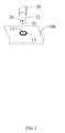
- FIG. 1 is a schematic view of an RF PCB, in accordance with an embodiment.
- FIG. 2 is a partial view of a probe of an EMC measuring device and the RF PCB of FIG. 1 , which is viewed at another angle.
- FIG. 3 is a schematic view of an RF PCB, in accordance with another embodiment.
- FIG. 4 is a partial view of a probe of an EMC measuring device and the RF PCB of FIG. 3 , which is viewed at another angle.
- an RF PCB 10 is shown.
- the RF PCB 10 is connected to a probe 20 of an EMC measuring device (not shown) when EMC of the RF PCB 10 needs to be measured.
- the EMC measuring device includes a probe 20 that is configured to connect to the RF PCB 10 .
- the probe 20 includes a probe pin 24 and a shielding barrel 22 surrounding the probe pin 24 .
- the shielding barrel 22 is tubular with one end opened, and thus includes an annular end surface 26 at the open end.
- the probe pin 24 extends along a central axis of the shielding barrel 22 to a plane that the end surface 26 is in.
- the RF PCB 10 includes a first surface 10 a and a second surface 10 b opposite to the first surface 10 a .
- the RF PCB 10 also includes an RF circuit 11 , an antenna 12 , a socket 13 , a test node 14 , and a ground node 15 .
- the RF circuit 11 , the antenna 12 , and the socket 13 are arranged on the first surface 10 a .
- the RF circuit 11 includes an output node 11 a and is configured to generate high frequency signals and output the high frequency signals through the output node 11 a .
- the antenna 12 is configured to emit the high frequency signals and is detachably connected to the output node 11 a via the socket 13 .
- the test node 14 and the ground node 15 are arranged on the second surface 10 b .
- the test node 14 is connected to the output node 11 a and is configured for contacting the probe pin 24 .
- the ground node 15 is annular and corresponds to the end surface 26 .
- the inner diameter of the ground node 15 is less than that of the end surface 26 , while the outer diameter of the ground node 15 is greater than that of the end surface 26 .
- the ground node 15 is connected to the ground wire of the RF circuit 11 and surrounds the test node 14 , centering on the test node 14 .
- the antenna 12 is removed from the socket 13 to avoid emitting the high frequency signals.
- the probe 20 is then connected to the RF PCB 10 such that the probe pin 24 contacts the test node 14 and the end surface 26 contacts the ground node 15 .
- the shielding barrel 22 cooperates with the RF PCB 10 to provide an EMC shield for the probe pin 24 .
- the shielding barrel can be conveniently grounded.
- an RF PCB 30 is shown. Comparing to the above mentioned embodiment in FIGS. 1-2 , the differences are: the antenna 19 is formed on the RF PCB 10 directly; the antenna is connected to the output node 11 a through a switch 18 ; and the ground node 16 is shaped as a rectangular frame. In measurement, the antenna 19 is removed by turn off the switch 18 . The ground node 16 can also contact the end surface 26 while the probe pin 24 contacts the test node 14 .
- the shape of the ground node is not limited to the present embodiments as long as it can contact the end surface 26 while the probe pin 24 contacting the test node 14 .
- the test node 14 and the ground node 15 can be arranged on the first surface 10 a.
Landscapes
- Engineering & Computer Science (AREA)
- Microelectronics & Electronic Packaging (AREA)
- General Engineering & Computer Science (AREA)
- Physics & Mathematics (AREA)
- General Physics & Mathematics (AREA)
- Measuring Leads Or Probes (AREA)
- Waveguide Aerials (AREA)
- Shielding Devices Or Components To Electric Or Magnetic Fields (AREA)
- Testing Of Individual Semiconductor Devices (AREA)
Abstract
Description
- 1. Technical Field
- The present disclosure relates to printed circuit boards (PCBs) and, particularly, to a radio frequency (RF) PCB.
- 2. Description of Related Art
- RF products usually include a PCB and an antenna. The PCB includes an RF circuit, which generates high frequency signals, and a connection node connecting to the antenna. Thus, the high frequency signals can be emitted by the antenna. The RF products need to pass an electromagnetic compatibility (EMC) test, where the EMC is measured using a direct measurement method. In the direct measurement method, the antenna is removed and an EMC measuring device is connected to the connection node. In particular, the EMC measuring device includes a probe. The probe includes a probe pin and a shielding barrel surrounding the probe pin. The probe pin contacts the connection node, while the shielding barrel connects to the ground of the PCB. The shielding barrel cooperates with the PCB to enclose the probe pin to provide EMC shield for the probe pin. However, current PCBs do not have a ground node around the connection node to allow the shielding barrel to be directly connected. Thus, the shielding barrel needs to be grounded with extra wires, which is inconvenient.
- Therefore, it is desirable to provide a radio frequency PCB to overcome the above mentioned limitations.
- Many aspects of the present disclosure should be better understood with reference to the following drawings.
-
FIG. 1 is a schematic view of an RF PCB, in accordance with an embodiment. -
FIG. 2 is a partial view of a probe of an EMC measuring device and the RF PCB ofFIG. 1 , which is viewed at another angle. -
FIG. 3 is a schematic view of an RF PCB, in accordance with another embodiment. -
FIG. 4 is a partial view of a probe of an EMC measuring device and the RF PCB ofFIG. 3 , which is viewed at another angle. - Embodiments of the present disclosure will now be described in detail with reference to the drawings.
- Referring to
FIGS. 1 and 2 , anRF PCB 10, according to an embodiment, is shown. TheRF PCB 10 is connected to aprobe 20 of an EMC measuring device (not shown) when EMC of theRF PCB 10 needs to be measured. The EMC measuring device includes aprobe 20 that is configured to connect to theRF PCB 10. Theprobe 20 includes aprobe pin 24 and ashielding barrel 22 surrounding theprobe pin 24. Theshielding barrel 22 is tubular with one end opened, and thus includes anannular end surface 26 at the open end. Theprobe pin 24 extends along a central axis of theshielding barrel 22 to a plane that theend surface 26 is in. - The RF PCB 10 includes a
first surface 10 a and asecond surface 10 b opposite to thefirst surface 10 a. TheRF PCB 10 also includes anRF circuit 11, anantenna 12, asocket 13, atest node 14, and aground node 15. TheRF circuit 11, theantenna 12, and thesocket 13 are arranged on thefirst surface 10 a. TheRF circuit 11 includes an output node 11 a and is configured to generate high frequency signals and output the high frequency signals through the output node 11 a. Theantenna 12 is configured to emit the high frequency signals and is detachably connected to the output node 11 a via thesocket 13. Thetest node 14 and theground node 15 are arranged on thesecond surface 10 b. Thetest node 14 is connected to the output node 11 a and is configured for contacting theprobe pin 24. Theground node 15 is annular and corresponds to theend surface 26. The inner diameter of theground node 15 is less than that of theend surface 26, while the outer diameter of theground node 15 is greater than that of theend surface 26. Theground node 15 is connected to the ground wire of theRF circuit 11 and surrounds thetest node 14, centering on thetest node 14. - During measurement of the EMC, the
antenna 12 is removed from thesocket 13 to avoid emitting the high frequency signals. Theprobe 20 is then connected to the RF PCB 10 such that theprobe pin 24 contacts thetest node 14 and theend surface 26 contacts theground node 15. Thus, theshielding barrel 22 cooperates with the RF PCB 10 to provide an EMC shield for theprobe pin 24. As such, the shielding barrel can be conveniently grounded. - Referring to
FIGS. 3 and 4 , anRF PCB 30, according to another embodiment, is shown. Comparing to the above mentioned embodiment inFIGS. 1-2 , the differences are: theantenna 19 is formed on theRF PCB 10 directly; the antenna is connected to the output node 11 a through aswitch 18; and theground node 16 is shaped as a rectangular frame. In measurement, theantenna 19 is removed by turn off theswitch 18. Theground node 16 can also contact theend surface 26 while theprobe pin 24 contacts thetest node 14. - It should be understood that, the shape of the ground node is not limited to the present embodiments as long as it can contact the
end surface 26 while theprobe pin 24 contacting thetest node 14. In alternative embodiments, thetest node 14 and theground node 15 can be arranged on thefirst surface 10 a. - It will be understood that the above particular embodiments is shown and described by way of illustration only. The principles and the features of the present disclosure may be employed in various and numerous embodiment thereof without departing from the scope of the disclosure as claimed. The above-described embodiments illustrate the scope of the disclosure but do not restrict the scope of the disclosure.
Claims (7)
Applications Claiming Priority (3)
| Application Number | Priority Date | Filing Date | Title |
|---|---|---|---|
| CN2011100751581A CN102711361A (en) | 2011-03-28 | 2011-03-28 | Circuit board |
| CN201110075158 | 2011-03-28 | ||
| CN201110075158.1 | 2011-03-28 |
Publications (2)
| Publication Number | Publication Date |
|---|---|
| US20120249381A1 true US20120249381A1 (en) | 2012-10-04 |
| US8659489B2 US8659489B2 (en) | 2014-02-25 |
Family
ID=46903858
Family Applications (1)
| Application Number | Title | Priority Date | Filing Date |
|---|---|---|---|
| US13/157,322 Expired - Fee Related US8659489B2 (en) | 2011-03-28 | 2011-06-10 | Radio frequency printed circuit board |
Country Status (3)
| Country | Link |
|---|---|
| US (1) | US8659489B2 (en) |
| CN (1) | CN102711361A (en) |
| TW (1) | TWI452947B (en) |
Cited By (3)
| Publication number | Priority date | Publication date | Assignee | Title |
|---|---|---|---|---|
| CN106160884A (en) * | 2016-07-18 | 2016-11-23 | 珠海迈科智能科技股份有限公司 | A kind of WIFI signal test device |
| EP3104465A1 (en) * | 2015-06-11 | 2016-12-14 | FairPhone B.V. | Connector for an electronic device |
| US10594845B2 (en) | 2015-06-10 | 2020-03-17 | Fairphone B.V. | Electronic device |
Families Citing this family (7)
| Publication number | Priority date | Publication date | Assignee | Title |
|---|---|---|---|---|
| CN107850625B (en) * | 2016-03-18 | 2020-04-24 | 深圳市艾励美特科技有限公司 | Radio frequency detection device |
| CN106053980B (en) * | 2016-05-24 | 2018-01-12 | 北京航空航天大学 | A kind of backboard electromagnetic compatibility detection device and method |
| TWI651028B (en) * | 2018-03-14 | 2019-02-11 | 明泰科技股份有限公司 | Pad structure for RF testing |
| CN109709360A (en) * | 2019-03-05 | 2019-05-03 | 镇江蓝箭电子有限公司 | A flexible test head for PCB signal testing |
| CN112305277B (en) * | 2020-10-29 | 2021-10-26 | 深圳合一测试科技有限公司 | Embedded tuned circuit board probe for testing radio frequency signals based on radio frequency-free test seat |
| WO2022227063A1 (en) * | 2021-04-30 | 2022-11-03 | 华为技术有限公司 | Lga pad structure, manufacturing method, chip module, printed circuit board, and device |
| CN115411534A (en) * | 2022-08-10 | 2022-11-29 | 新华三技术有限公司 | Test grounding device, test equipment and circuit test method |
Citations (4)
| Publication number | Priority date | Publication date | Assignee | Title |
|---|---|---|---|---|
| US6380752B1 (en) * | 1998-11-11 | 2002-04-30 | Nec Corporation | IC socket |
| US6456070B1 (en) * | 1999-01-13 | 2002-09-24 | Taiyo Yuden Co., Ltd. | Method and device for measuring intensity of electromagnetic field, method and device for measuring current-voltage distribution, and method for judging quality of electronic device, and electronic device therefor |
| US6696834B2 (en) * | 1997-03-13 | 2004-02-24 | Ricoh Company, Ltd. | Magnetic field probe having a shielding layer to protect lead wires with an isolating layer |
| US7642973B2 (en) * | 2004-12-22 | 2010-01-05 | Panasonic Corporation | Electromagnetic wave analysis apparatus and design support apparatus |
Family Cites Families (4)
| Publication number | Priority date | Publication date | Assignee | Title |
|---|---|---|---|---|
| JP2000147041A (en) * | 1998-11-12 | 2000-05-26 | Mitsubishi Electric Corp | Electronic equipment testing equipment |
| CN101004426A (en) * | 2006-01-20 | 2007-07-25 | 佛山市顺德区顺达电脑厂有限公司 | Radiated noise arrester of ground wire of bar for probing electric signals |
| TWM358968U (en) * | 2008-12-31 | 2009-06-11 | Universal Scient Ind Co Ltd | Probe device |
| TWI460438B (en) * | 2009-07-17 | 2014-11-11 | Universal Scient Ind Shanghai | Antenna test system, test method and test fixture |
-
2011
- 2011-03-28 CN CN2011100751581A patent/CN102711361A/en active Pending
- 2011-04-06 TW TW100111717A patent/TWI452947B/en not_active IP Right Cessation
- 2011-06-10 US US13/157,322 patent/US8659489B2/en not_active Expired - Fee Related
Patent Citations (4)
| Publication number | Priority date | Publication date | Assignee | Title |
|---|---|---|---|---|
| US6696834B2 (en) * | 1997-03-13 | 2004-02-24 | Ricoh Company, Ltd. | Magnetic field probe having a shielding layer to protect lead wires with an isolating layer |
| US6380752B1 (en) * | 1998-11-11 | 2002-04-30 | Nec Corporation | IC socket |
| US6456070B1 (en) * | 1999-01-13 | 2002-09-24 | Taiyo Yuden Co., Ltd. | Method and device for measuring intensity of electromagnetic field, method and device for measuring current-voltage distribution, and method for judging quality of electronic device, and electronic device therefor |
| US7642973B2 (en) * | 2004-12-22 | 2010-01-05 | Panasonic Corporation | Electromagnetic wave analysis apparatus and design support apparatus |
Cited By (5)
| Publication number | Priority date | Publication date | Assignee | Title |
|---|---|---|---|---|
| US10594845B2 (en) | 2015-06-10 | 2020-03-17 | Fairphone B.V. | Electronic device |
| US11005979B2 (en) | 2015-06-10 | 2021-05-11 | Fairphone B.V. | Electronic device |
| EP3104465A1 (en) * | 2015-06-11 | 2016-12-14 | FairPhone B.V. | Connector for an electronic device |
| CN106160884A (en) * | 2016-07-18 | 2016-11-23 | 珠海迈科智能科技股份有限公司 | A kind of WIFI signal test device |
| CN106160884B (en) * | 2016-07-18 | 2018-09-14 | 珠海迈科智能科技股份有限公司 | A kind of WIFI signal test device |
Also Published As
| Publication number | Publication date |
|---|---|
| TW201240532A (en) | 2012-10-01 |
| TWI452947B (en) | 2014-09-11 |
| CN102711361A (en) | 2012-10-03 |
| US8659489B2 (en) | 2014-02-25 |
Similar Documents
| Publication | Publication Date | Title |
|---|---|---|
| US8659489B2 (en) | Radio frequency printed circuit board | |
| CN104345186B (en) | High-frequency probe card for detecting photoelectric element | |
| US9864001B2 (en) | Electronic device and testing system | |
| TW201415039A (en) | Systems, devices and methods related to near-field electromagnetic probes and scanners | |
| CN204740272U (en) | A passive probe | |
| US9470716B2 (en) | Probe module | |
| US8786298B2 (en) | Apparatus and method for near field scan calibration | |
| TW201413257A (en) | Sensing element and signal sensing device with the same | |
| CN107367648B (en) | Microwave Monolithic Circuit Immunity Test Fixture | |
| US9927484B2 (en) | Radio frequency probe apparatus | |
| TWI522623B (en) | Probe module (1) | |
| CN217180969U (en) | Micro coaxial radio frequency probe card | |
| JP2012103028A (en) | Testing board | |
| US10101362B2 (en) | Probe module with high stability | |
| US10897102B2 (en) | Connector structure | |
| US20120098732A1 (en) | Emi detection apparatus | |
| CN104714055B (en) | Detection jig | |
| KR101421048B1 (en) | Device For Testing Semiconductor On Mounted Active Element Chip | |
| CN203551671U (en) | High-frequency electric field probe | |
| CN104678191A (en) | Device and method for measuring radiation intensity of integrated circuit on basis of TEM test box | |
| CN108646169A (en) | A kind of BOSA test methods and system | |
| CN110417492B (en) | A Method for Detecting In-band Receiving Spurs of Antennas | |
| KR101328095B1 (en) | Optical testing apparatus | |
| KR101895012B1 (en) | A inserting type high frequency signal transmission connector and probe card using the connector | |
| CN105807207B (en) | The detection probe of power module |
Legal Events
| Date | Code | Title | Description |
|---|---|---|---|
| AS | Assignment |
Owner name: HON HAI PRECISION INDUSTRY CO., LTD., TAIWAN Free format text: ASSIGNMENT OF ASSIGNORS INTEREST;ASSIGNORS:WANG, JUN-WEI;TSEN, CHUN-CHIEH;REEL/FRAME:026421/0448 Effective date: 20101204 Owner name: HONG FU JIN PRECISION INDUSTRY (SHENZHEN) CO., LTD Free format text: ASSIGNMENT OF ASSIGNORS INTEREST;ASSIGNORS:WANG, JUN-WEI;TSEN, CHUN-CHIEH;REEL/FRAME:026421/0448 Effective date: 20101204 |
|
| FEPP | Fee payment procedure |
Free format text: MAINTENANCE FEE REMINDER MAILED (ORIGINAL EVENT CODE: REM.) |
|
| AS | Assignment |
Owner name: HONGFUJIN PRECISION ELECTRONICS(TIANJIN)CO.,LTD., Free format text: ASSIGNMENT OF ASSIGNORS INTEREST;ASSIGNORS:HONG FU JIN PRECISION INDUSTRY (SHENZHEN) CO., LTD.;HON HAI PRECISION INDUSTRY CO., LTD.;REEL/FRAME:045501/0324 Effective date: 20180112 |
|
| LAPS | Lapse for failure to pay maintenance fees |
Free format text: PATENT EXPIRED FOR FAILURE TO PAY MAINTENANCE FEES (ORIGINAL EVENT CODE: EXP.) |
|
| STCH | Information on status: patent discontinuation |
Free format text: PATENT EXPIRED DUE TO NONPAYMENT OF MAINTENANCE FEES UNDER 37 CFR 1.362 |
|
| FP | Lapsed due to failure to pay maintenance fee |
Effective date: 20180225 |