US20120249253A1 - Mems vibrator and oscillator - Google Patents
Mems vibrator and oscillator Download PDFInfo
- Publication number
- US20120249253A1 US20120249253A1 US13/431,354 US201213431354A US2012249253A1 US 20120249253 A1 US20120249253 A1 US 20120249253A1 US 201213431354 A US201213431354 A US 201213431354A US 2012249253 A1 US2012249253 A1 US 2012249253A1
- Authority
- US
- United States
- Prior art keywords
- beam portion
- mems vibrator
- electrode
- face
- substrate
- Prior art date
- Legal status (The legal status is an assumption and is not a legal conclusion. Google has not performed a legal analysis and makes no representation as to the accuracy of the status listed.)
- Granted
Links
- 239000000758 substrate Substances 0.000 claims abstract description 54
- 230000007423 decrease Effects 0.000 claims abstract description 16
- 239000003990 capacitor Substances 0.000 claims description 3
- 238000004519 manufacturing process Methods 0.000 description 24
- 238000004088 simulation Methods 0.000 description 21
- 238000000034 method Methods 0.000 description 20
- 238000005530 etching Methods 0.000 description 16
- 239000012535 impurity Substances 0.000 description 11
- XUKUURHRXDUEBC-SXOMAYOGSA-N (3s,5r)-7-[2-(4-fluorophenyl)-3-phenyl-4-(phenylcarbamoyl)-5-propan-2-ylpyrrol-1-yl]-3,5-dihydroxyheptanoic acid Chemical compound C=1C=CC=CC=1C1=C(C=2C=CC(F)=CC=2)N(CC[C@@H](O)C[C@H](O)CC(O)=O)C(C(C)C)=C1C(=O)NC1=CC=CC=C1 XUKUURHRXDUEBC-SXOMAYOGSA-N 0.000 description 8
- XUIMIQQOPSSXEZ-UHFFFAOYSA-N Silicon Chemical compound [Si] XUIMIQQOPSSXEZ-UHFFFAOYSA-N 0.000 description 7
- 229910052710 silicon Inorganic materials 0.000 description 7
- 239000010703 silicon Substances 0.000 description 7
- KRHYYFGTRYWZRS-UHFFFAOYSA-N Fluorane Chemical compound F KRHYYFGTRYWZRS-UHFFFAOYSA-N 0.000 description 6
- 238000000059 patterning Methods 0.000 description 5
- 238000005229 chemical vapour deposition Methods 0.000 description 4
- 239000000470 constituent Substances 0.000 description 4
- 239000000463 material Substances 0.000 description 4
- ZOXJGFHDIHLPTG-UHFFFAOYSA-N Boron Chemical compound [B] ZOXJGFHDIHLPTG-UHFFFAOYSA-N 0.000 description 3
- 229910052796 boron Inorganic materials 0.000 description 3
- 230000008859 change Effects 0.000 description 3
- 230000010355 oscillation Effects 0.000 description 3
- 229910021420 polycrystalline silicon Inorganic materials 0.000 description 3
- 238000004544 sputter deposition Methods 0.000 description 3
- 238000009623 Bosch process Methods 0.000 description 2
- 229910018503 SF6 Inorganic materials 0.000 description 2
- VYPSYNLAJGMNEJ-UHFFFAOYSA-N Silicium dioxide Chemical compound O=[Si]=O VYPSYNLAJGMNEJ-UHFFFAOYSA-N 0.000 description 2
- 230000008901 benefit Effects 0.000 description 2
- 230000000052 comparative effect Effects 0.000 description 2
- 238000000151 deposition Methods 0.000 description 2
- 230000008021 deposition Effects 0.000 description 2
- 238000002161 passivation Methods 0.000 description 2
- 239000004065 semiconductor Substances 0.000 description 2
- 229910052814 silicon oxide Inorganic materials 0.000 description 2
- DDFHBQSCUXNBSA-UHFFFAOYSA-N 5-(5-carboxythiophen-2-yl)thiophene-2-carboxylic acid Chemical compound S1C(C(=O)O)=CC=C1C1=CC=C(C(O)=O)S1 DDFHBQSCUXNBSA-UHFFFAOYSA-N 0.000 description 1
- 229910052581 Si3N4 Inorganic materials 0.000 description 1
- 239000004809 Teflon Substances 0.000 description 1
- 229920006362 Teflon® Polymers 0.000 description 1
- ATJFFYVFTNAWJD-UHFFFAOYSA-N Tin Chemical compound [Sn] ATJFFYVFTNAWJD-UHFFFAOYSA-N 0.000 description 1
- 239000000919 ceramic Substances 0.000 description 1
- 229910003460 diamond Inorganic materials 0.000 description 1
- 239000010432 diamond Substances 0.000 description 1
- 238000009826 distribution Methods 0.000 description 1
- 230000000694 effects Effects 0.000 description 1
- WRQGPGZATPOHHX-UHFFFAOYSA-N ethyl 2-oxohexanoate Chemical compound CCCCC(=O)C(=O)OCC WRQGPGZATPOHHX-UHFFFAOYSA-N 0.000 description 1
- 239000011521 glass Substances 0.000 description 1
- 238000009616 inductively coupled plasma Methods 0.000 description 1
- 239000012212 insulator Substances 0.000 description 1
- 238000002955 isolation Methods 0.000 description 1
- 239000011259 mixed solution Substances 0.000 description 1
- 230000004048 modification Effects 0.000 description 1
- 238000012986 modification Methods 0.000 description 1
- 230000003647 oxidation Effects 0.000 description 1
- 238000007254 oxidation reaction Methods 0.000 description 1
- 230000001590 oxidative effect Effects 0.000 description 1
- 230000000149 penetrating effect Effects 0.000 description 1
- 238000001020 plasma etching Methods 0.000 description 1
- 229910052594 sapphire Inorganic materials 0.000 description 1
- 239000010980 sapphire Substances 0.000 description 1
- HQVNEWCFYHHQES-UHFFFAOYSA-N silicon nitride Chemical compound N12[Si]34N5[Si]62N3[Si]51N64 HQVNEWCFYHHQES-UHFFFAOYSA-N 0.000 description 1
- 239000000126 substance Substances 0.000 description 1
- SFZCNBIFKDRMGX-UHFFFAOYSA-N sulfur hexafluoride Chemical compound FS(F)(F)(F)(F)F SFZCNBIFKDRMGX-UHFFFAOYSA-N 0.000 description 1
- 229960000909 sulfur hexafluoride Drugs 0.000 description 1
- 229920003002 synthetic resin Polymers 0.000 description 1
- 239000000057 synthetic resin Substances 0.000 description 1
- 238000001039 wet etching Methods 0.000 description 1
Images


Classifications
-
- H—ELECTRICITY
- H03—ELECTRONIC CIRCUITRY
- H03H—IMPEDANCE NETWORKS, e.g. RESONANT CIRCUITS; RESONATORS
- H03H3/00—Apparatus or processes specially adapted for the manufacture of impedance networks, resonating circuits, resonators
- H03H3/007—Apparatus or processes specially adapted for the manufacture of impedance networks, resonating circuits, resonators for the manufacture of electromechanical resonators or networks
- H03H3/0072—Apparatus or processes specially adapted for the manufacture of impedance networks, resonating circuits, resonators for the manufacture of electromechanical resonators or networks of microelectro-mechanical resonators or networks
-
- H—ELECTRICITY
- H03—ELECTRONIC CIRCUITRY
- H03H—IMPEDANCE NETWORKS, e.g. RESONANT CIRCUITS; RESONATORS
- H03H9/00—Networks comprising electromechanical or electro-acoustic elements; Electromechanical resonators
- H03H9/24—Constructional features of resonators of material which is not piezoelectric, electrostrictive, or magnetostrictive
- H03H9/2405—Constructional features of resonators of material which is not piezoelectric, electrostrictive, or magnetostrictive of microelectro-mechanical resonators
- H03H9/2447—Beam resonators
- H03H9/2457—Clamped-free beam resonators
Definitions
- the present invention relates to a MEMS vibrator and an oscillator.
- JP-A-2010-162629 discloses a MEMS vibrator having a fixed electrode and a movable electrode, in which the movable electrode is driven by electrostatic force generated between the electrodes. Output of such an electrostatic-type MEMS vibrator is generated by a change in capacitance between the fixed electrode and the movable electrode when the MEMS vibrator is driven. Therefore, the larger the crossing area (area of a region where the electrodes overlap each other) of the fixed electrode and the movable electrode is, the higher the output is.
- a driving frequency is a natural frequency of a vibrator, and determined by the shape and dimensions of the vibrator.
- Various shapes of MEMS vibrators driven in a frequency band from several kHz to several GHz have been proposed so far.
- the driving frequency is determined by the length and thickness of a beam portion (movable electrode). When the thickness is constant, the great length of the beam portion makes the frequency low, and the small length thereof makes the frequency high.
- the crossing area of the fixed electrode and the beam portion is reduced because of the small length of the beam portion, resulting in low output in some cases.
- the vibrator is considered as an equivalent circuit, the series resistance is high.
- phase reversal is insufficient as the resistance is increased, failing to satisfy oscillation conditions in some cases.
- An advantage of some aspects of the invention is to provide a MEMS vibrator having high output and driven at a high frequency.
- Another advantage of some aspects of the invention is to provide an oscillator having the MEMS vibrator described above.
- An aspect of the invention is directed to a MEMS vibrator including: a first electrode fixed to a surface of a substrate; and a second electrode having a beam portion including a second face facing a first face of the first electrode, and a supporting portion supporting the beam portion and fixed to the surface of the substrate, wherein the beam portion has a first portion whose length in a normal direction of the first face of the beam portion monotonically decreases toward a tip of the beam portion.
- the beam portion may have a second portion whose length in the normal direction of the beam portion is constant, the first portion may include the tip, the second portion may be contiguous with the first portion and supported by the supporting portion, and the MEMS vibrator may satisfy the following expression (1):
- L is the length of a region of the beam portion overlapping the first electrode, in a direction from the supporting portion toward the tip
- L 2 is the length of a region of the second portion overlapping the first electrode, in the direction from the supporting portion toward the tip.
- the normal of the first face may be parallel to the normal of the surface of the substrate.
- the normal of the first face may be perpendicular to the normal of the surface of the substrate.
- Another aspect of the invention is directed to an oscillator including the MEMS vibrator according to the aspect of the invention.
- the series resistance can be prevented from being increased, and the phase can be reversed. Accordingly, the oscillator described above can satisfy oscillation conditions, and therefore can stably oscillate the MEMS vibrator according to the aspect of the invention at a high frequency.
- FIG. 1 is a cross-sectional view schematically showing a MEMS vibrator according to an embodiment.
- FIG. 2 is a plan view schematically showing the MEMS vibrator according to the embodiment.
- FIG. 3 is a cross-sectional view schematically showing a manufacturing step of the MEMS vibrator according to the embodiment.
- FIG. 4 is a cross-sectional view schematically showing a manufacturing step of the MEMS vibrator according to the embodiment.
- FIG. 5 is a cross-sectional view schematically showing a manufacturing step of the MEMS vibrator according to the embodiment.
- FIG. 6 is a cross-sectional view schematically showing a manufacturing step of the MEMS vibrator according to the embodiment.
- FIG. 7 is a cross-sectional view schematically showing a manufacturing step of the MEMS vibrator according to the embodiment.
- FIG. 8 is a cross-sectional view schematically showing a manufacturing step of the MEMS vibrator according to the embodiment.
- FIG. 9 is a cross-sectional view schematically showing a MEMS vibrator according to a first modified example of the embodiment.
- FIG. 10 is a plan view schematically showing a MEMS vibrator according to a second modified example of the embodiment.
- FIG. 11 is a cross-sectional view schematically showing the MEMS vibrator according to the second modified example of the embodiment.
- FIG. 12 is a cross-sectional view schematically showing the MEMS vibrator according to the second modified example of the embodiment.
- FIG. 13 is a cross-sectional view schematically showing a manufacturing step of the MEMS vibrator according to the second modified example of the embodiment.
- FIG. 14 is a cross-sectional view schematically showing a manufacturing step of the MEMS vibrator according to the second modified example of the embodiment.
- FIG. 16 is a plan view schematically showing a MEMS vibrator according to a third modified example of the embodiment.
- FIG. 17 is a graph showing the results of a first simulation in an experimental example.
- FIGS. 18A to 18C each schematically show a beam portion used for the first simulation in the experimental example.
- FIG. 19 is a graph showing the results of a second simulation in an experimental example.
- FIGS. 20D to 20G each schematically show a beam portion used for the second simulation in the experimental example.
- FIG. 21 schematically shows an oscillator according to the embodiment.
- FIG. 1 is a cross-sectional view schematically showing a MEMS vibrator 100 according to the embodiment.
- FIG. 2 is a plan view schematically showing the MEMS vibrator 100 according to the embodiment.
- FIG. 1 is the cross-sectional view taken along line I-I of FIG. 2 .
- the MEMS vibrator 100 includes a substrate 10 , a first electrode 20 , and a second electrode 30 .
- the substrate 10 can have a supporting substrate 12 , a first under layer 14 , and a second under layer 16 .
- the first under layer 14 is formed on the supporting substrate 12 .
- a trench insulating layer As the first under layer 14 , a trench insulating layer, a LOCOS (Local Oxidation of Silicon) insulating layer, or a semi-recessed LOCOS insulating layer, for example, can be used.
- the first under layer 14 can electrically isolate the MEMS vibrator 100 from another element (not shown) formed in the supporting substrate 12 .
- the second under layer 16 is formed on the first under layer 14 .
- the material of the second under layer 16 is silicon nitride, for example.
- the second under layer 16 can function as an etching stopper layer in a release step described later.
- the first electrode 20 is formed on the substrate 10 and fixed to a surface 11 of the substrate 10 .
- the planar shape (shape as viewed from a direction of the normal P of the surface 11 of the substrate 10 ) of the first electrode 20 is, for example, a rectangle as shown in FIG. 2 .
- the first electrode 20 has a first face 21 .
- the first face 21 which can also be referred to as an upper face of the first electrode 20 , is a flat face.
- the normal Q of the first face 21 is parallel to the normal P of the surface 11 of the substrate 10 .
- the thickness (length in the Z-axis direction) of the first electrode 20 is, for example, from 0.1 ⁇ m to 100 ⁇ m.
- the second electrode 30 is formed spaced apart from the first electrode 20 .
- the second electrode 30 has a supporting portion 32 formed on the substrate 10 , and a beam portion 34 supported by the supporting portion 32 and arranged above the first electrode 20 .
- the supporting portion 32 is fixed to the surface 11 of the substrate 10 .
- the supporting portion 32 supports the beam portion 34 . That is, the second electrode 30 is formed in a cantilevered manner.
- the beam portion 34 has a second face 31 facing the first face 21 of the first electrode 20 . More specifically, the second face 31 is parallel to the first face 21 . That is, the normal Q of the first face 21 can be rephrased as the normal Q of the second face 31 .
- the second face 31 which can also be referred to as a lower face of the beam portion 34 , is a flat face.
- the beam portion 34 overlaps the first electrode 20 in a region A.
- the planar shape of the beam portion 34 is a rectangle with a length W (also referred to as “width W”) in the Y-axis direction being as the length of its short side.
- the beam portion 34 has a first portion 36 and a second portion 38 .
- the first portion 36 has a shape in which a length T (length in the Z-axis direction) in a direction of the normal Q of the first face 21 of the first electrode 20 decreases toward a tip 35 of the beam portion 34 (toward the +X-direction).
- the length T also referred to as “thickness T”
- the first portion 36 may be configured such that the length T in the Z-axis direction does not remain the same in any section on the way from the supporting portion 32 toward the tip 35 but continuously changes toward the tip 35 .
- the first portion 36 may have an inclined face 37 which is inclined to the first face 21 and the second face 31 as shown in FIG. 1 .
- the cross-sectional shape of the first portion 36 may be a triangle.
- the first portion 36 can include the tip 35 .
- the first portion 36 is arranged in the region A of the beam portion 34 overlapping the first electrode 20 . That is, in plan view (viewed from the normal-P-direction of the surface 11 of the substrate 10 ) as shown in FIG. 2 , the first portion 36 is arranged inside the outer circumference of the first electrode 20 .
- the planar shape of the first portion 36 may be a rectangle as shown in FIG. 2 .
- the length T (length in the Z-axis direction) of the second portion 38 in the normal-Q-direction of the first face 21 of the beam portion 34 is constant.
- the second portion 38 is contiguous with the first portion 36 and supported by the supporting portion 32 .
- the second portion 38 is adjacent to, for example, the supporting portion 32 .
- the cross-sectional shape of the second portion 38 may be a rectangle as shown in FIG. 1 .
- a portion of the second portion 38 is arranged in the region A of the beam portion 34 overlapping the first electrode 20 .
- the planar shape of the second portion 38 may be a rectangle as shown in FIG. 2 .
- the thickness (length in the Z-axis direction) of the second portion 38 is, for example, from 0.1 ⁇ m to 100 ⁇ m.
- the MEMS vibrator 100 When it is defined that a length of the region A of the beam portion 34 overlapping the first electrode 20 , in a direction from the supporting portion 32 toward the tip 35 (X-axis direction), is L, and that a length of the region A of the second portion 38 overlapping the first electrode 20 , in the X-axis direction, is L 2 , the MEMS vibrator 100 preferably satisfies the following expression (1). With this configuration, the MEMS vibrator 100 can be driven at a higher frequency (the details will be described later).
- the material of the first electrode 20 and the second electrode 30 is, for example, polycrystalline silicon doped with a predetermined impurity to provide conductivity.
- the beam portion 34 can be vibrated by electrostatic force generated between the electrodes 20 and 30 .
- the first electrode 20 and the supporting portion 32 of the second electrode 30 can be connected to wiring (not shown) for applying a voltage between the electrodes 20 and 30 .
- the MEMS vibrator 100 may have a covering structure which airtightly seals the first electrode 20 and the second electrode 30 in a reduced-pressure state. With this configuration, it is possible to reduce the air resistance of the beam portion 34 during its vibration.
- the MEMS vibrator 100 has, for example, the following features.
- the beam portion 34 has the first portion 36 whose length T (length in the Z-axis direction) in the normal-Q-direction of the beam portion 34 decreases toward the tip 35 of the beam portion 34 (toward the +X-direction). That is, in the MEMS vibrator 100 , the mass of the beam portion 34 can be reduced compared to the case where the length in the Z-axis direction is constant. Therefore, the mass of the beam portion 34 can be reduced without reducing the region A (crossing area) where the first electrode 20 overlaps the beam portion 34 . In short, it is no need to reduce the capacitance between the first electrode 20 and the beam portion 34 for driving the MEMS vibrator at a high frequency. Accordingly, the MEMS vibrator 100 has high output and can be driven at a high frequency.
- the length T of the first portion 36 of the beam portion 34 in the Z-axis direction can continuously change toward the tip 35 . Therefore, it is possible to prevent the MEMS vibrator 100 from being driven in another driving mode different from a desired driving mode. For example, when the length of the beam portion in the Z-axis direction changes in a stepwise manner, the MEMS vibrator cannot be driven in a desired driving mode in some cases because another driving mode is generated in a step portion.
- FIGS. 3 to 8 are cross-sectional views schematically showing manufacturing steps of the MEMS vibrator 100 according to the embodiment.
- the first under layer 14 and the second under layer 16 are formed in this order on the supporting substrate 12 to obtain the substrate 10 .
- the first under layer 14 is formed by, for example, an STI (Shallow Trench Isolation) method or a LOCOS method.
- the second under layer 16 is formed by, for example, a CVD (Chemical Vapor Deposition) method or a sputtering method.
- the first electrode 20 is formed on the substrate 10 . More specifically, the first electrode 20 is formed by deposition by a CVD method, a sputtering method, or the like, and then by patterning using a photolithographic technique and an etching technique. Next, the first electrode 20 formed of, for example, polycrystalline silicon is doped with a predetermined impurity (for example, boron) to provide conductivity.
- a predetermined impurity for example, boron
- a sacrificial layer 40 is formed so as to cover the first electrode 20 .
- the sacrificial layer 40 is formed by, for example, thermally oxidizing the first electrode 20 .
- the material of the sacrificial layer 40 is, for example, silicon oxide.
- the thickness of the sacrificial layer 40 is, for example, from 0.01 ⁇ m to 100 ⁇ m. By the thickness of the sacrificial layer 40 , a distance between the first face 21 of the first electrode 20 and the second face 31 of the beam portion 34 is determined.
- the second electrode 30 is formed on the sacrificial layer 40 and the substrate 10 . More specifically, the second electrode 30 is formed by deposition by a CVD method, a sputtering method, or the like, and then by patterning using a photolithographic technique and an etching technique. Next, the second electrode 30 formed of polycrystalline silicon is doped with a predetermined impurity (for example, boron) to provide conductivity. Through the steps described above, the second electrode 30 having the beam portion 34 and the supporting portion 32 is formed.
- a predetermined impurity for example, boron
- a first resist layer R 1 having a first opening 1 is formed on the beam portion 34 by, for example, a known method.
- the end of the first opening 1 overlaps the tip 35 of the beam portion 34 .
- the length of the first opening 1 in the X-axis direction may be the same as the length (that is, the length L shown in FIGS. 1 and 2 ) of the first portion 36 of the beam portion 34 in the X-axis direction.
- the beam portion 34 is doped with a predetermined impurity B (for example, boron) using the first resist layer R 1 as a mask (a first doping step for the beam portion 34 ). Thereafter, the first resist layer R 1 is removed by, for example, a known method.
- a predetermined impurity B for example, boron
- a second resist layer R 2 having a second opening 2 is formed on the beam portion 34 by, for example, a known method.
- the end of the second opening 2 overlaps the tip 35 of the beam portion 34 .
- the length of the second opening 2 in the X-axis direction is smaller than the length of the first opening 1 in the X-axis direction.
- the beam portion 34 is doped with the predetermined impurity B using the second resist layer R 2 as a mask (a second doping step for the beam portion 34 ).
- the concentration of the impurity B to be doped in the second doping step may be the same as the concentration of the impurity B doped in the first doping step.
- the second resist layer R 2 is removed by, for example, a known method.
- a third resist layer R 3 having a third opening 3 is formed on the beam portion 34 by, for example, a known method.
- the end of the third opening 3 overlaps the tip 35 of the beam portion 34 .
- the length of the third opening 3 in the X-axis direction is smaller than the length of the second opening 2 in the X-axis direction.
- the beam portion 34 is doped with the predetermined impurity B using the third resist layer R 3 as a mask (a third doping step for the beam portion 34 ).
- the concentration of the impurity B to be doped in the third doping step may be the same as the concentration of the impurity B doped in the second doping step.
- the third resist layer R 3 is removed by, for example, a known method.
- the sacrificial layer 40 is removed (release step).
- the removal of the sacrificial layer 40 is performed by, for example, wet etching using hydrofluoric acid, buffered hydrofluoric acid (a mixed solution of hydrofluoric acid and ammonium fluoride), or the like.
- the second under layer 16 can function as an etching stopper layer.
- doping is selectively performed on the beam portion 34 three times.
- the number of times of doping is not particularly limited as long as it is two or more times.
- the inclined face 37 of the first portion 36 can be formed smoothly. That is, it is possible to form the first portion 36 whose length T in the Z-axis direction monotonically decreases toward the tip 35 .
- the doped impurity is diffused in the beam portion 34 . Therefore, when the patterning-doping step for the beam portion 34 is repeated about two times, the inclined face 37 can be sufficiently smoothly formed.
- the resist layer R 1 having the first opening 1 being large in size is first formed and then the resist layers having the openings being progressively reduced in size are formed.
- doping may be performed such that the resist layer R 3 having the third opening 3 being small in size is first formed and then the resist layers having the openings being progressively increased in size are formed.
- the MEMS vibrator 100 can be manufactured.
- FIG. 9 is a cross-sectional view schematically showing a MEMS vibrator 200 according to the first modified example of the embodiment, corresponding to FIG. 1 .
- members having functions similar to those of the constituent members of the MEMS vibrator 100 according to the embodiment are denoted by the same reference numerals and signs, and the detailed descriptions thereof are omitted.
- the beam portion 34 has the second portion 38 whose length T in the Z-axis direction is constant.
- the beam portion 34 does not have the second portion 38 but is composed of the first portion 36 whose length T in the Z-axis direction decreases toward the tip 35 of the beam portion 34 .
- the MEMS vibrator 200 it is possible similarly to the MEMS vibrator 100 to reduce the mass of the beam portion 34 without reducing the capacitance between the first electrode 20 and the beam portion 34 . Accordingly, the MEMS vibrator 200 has high output and can be driven at a high frequency.
- a manufacturing method of the MEMS vibrator 200 is basically the same as the manufacturing method of the MEMS vibrator 100 . Accordingly, the description thereof is omitted.
- the normal Q of the first face 21 of the first electrode 20 is parallel to the normal P of the surface 11 of the substrate 10 .
- the beam portion 34 can vibrate in the Z-axis direction parallel to the normal P of the surface 11 .
- a semiconductor substrate such as a silicon substrate, for example, can be used as the substrate 10 .
- the first electrode 20 is fixed to the surface 11 of the substrate 10 via an insulating layer 17 .
- the first face 21 of the first electrode 20 can be referred to as a side face of the first electrode 20 .
- the material of the insulating layer 17 is, for example, silicon oxide.
- the thickness (length in the Z-axis direction) of the insulating layer 17 is, for example, from 0.01 ⁇ m to 100 ⁇ m.
- the supporting portion 32 of the second electrode 30 is fixed to the surface 11 of the substrate 10 via the insulating layer 17 .
- the beam portion 34 is formed above the substrate 10 with a gap disposed between the beam portion and the substrate 10 .
- the second face 31 of the beam portion 34 can be referred to as a side face of the beam portion 34 .
- the cross-sectional shape of the second electrode 30 is, for example, a quadrilateral as shown in FIGS. 11 and 12 .
- the first portion 36 of the beam portion 34 has a shape in which the length T (length in the Y-axis direction) in the normal-Q-direction of the first face 21 of the first electrode 20 decreases toward the tip 35 of the beam portion 34 (toward the +X-direction).
- the length T of the first portion 36 in the Y-axis direction monotonically decreases toward the tip 35 . That is, as shown in FIG. 10 , the first portion 36 may be configured such that the length T in the Y-axis direction does not remain the same in any section on the way from the supporting portion 32 toward the tip 35 but continuously changes toward the tip 35 .
- the first portion 36 can have the inclined face 37 which is inclined to the first face 21 and the second face 31 .
- the planar shape of the first portion 36 may be a triangle.
- the first portion 36 can include the tip 35 .
- the first portion 36 is arranged in the region A overlapping the first electrode 20 . That is, the first portion 36 is arranged inside the outer circumference of the first electrode 20 as viewed from the normal-Q-direction of the first face 21 .
- the length (length in the Y-axis direction) of the second portion 38 in the normal-Q-direction of the first face 21 of the beam portion 34 is constant.
- the second portion 38 is contiguous with the first portion 36 and supported by the supporting portion 32 .
- the second portion 38 is adjacent to, for example, the supporting portion 32 .
- the planar shape of the second portion 38 may be a rectangle as shown in FIG. 10 .
- a portion of the second portion 38 is arranged in the region A of the beam portion 34 overlapping the first electrode 20 .
- the ratio (L 2 /L) of the length L 2 of the region A of the second portion 38 overlapping the first electrode 20 , in the direction from the supporting portion 32 toward the tip 35 (the X-axis direction), to the length L of the region A of the beam portion 34 overlapping the first electrode 20 , in the X-axis direction, satisfies the expression (1).
- the MEMS vibrator 300 can be driven at a higher frequency (the details will be described later).
- the MEMS vibrator 300 it is possible similarly to the MEMS vibrator 100 to reduce the mass of the beam portion 34 without reducing the capacitance between the first electrode 20 and the beam portion 34 . Accordingly, the MEMS vibrator 300 has high output and can be driven at a high frequency.
- FIGS. 13 and 14 are cross-sectional views schematically showing manufacturing steps of the MEMS vibrator 300 according to the second modified example of the embodiment.
- FIGS. 13 and 14 correspond to FIG. 11 .
- the silicon layer 18 is doped with the predetermined impurity B. With this doping, the silicon layer 18 can be converted to a conductive layer 28 provided with conductivity.
- the conductive layer 28 is patterned using a photolithographic technique and an etching technique to form the first electrode 20 and the second electrode 30 having the supporting portion 32 and the beam portion 34 .
- the patterning it is possible to form the first portion 36 whose length T in the Y-axis direction decreases toward the tip 35 of the beam portion 34 , and the second portion 38 whose length Tin the Y-axis direction is constant.
- Etching in the patterning may be performed using, for example, inductively coupled plasma reactive ion etching (ICP-RIE), or may be performed by the so-called Bosch process in which etching and etching sidewall passivation are repeated.
- ICP-RIE inductively coupled plasma reactive ion etching
- etching is performed by the Bosch process for example, isotropic etching is performed using sulfur hexafluoride (SF 6 ) in an etching step, and the sidewall is passivated using a teflon (registered trademark) based gas (C 4 F 8 or the like) in a passivation step, making it possible to suppress etching in the lateral direction (the X-axis direction and the Y-axis direction).
- SF 6 sulfur hexafluoride
- C 4 F 8 registered trademark
- the insulating layer 17 is etched using the first electrode 20 and the second electrode 30 as masks. By the etching, the insulating layer 17 below the beam portion 34 is removed. The insulating layer 17 below the first electrode 20 and the supporting portion 32 is not removed but side-etched in the illustrated example. Although not shown in the drawing, a through-hole penetrating from an upper face to a lower face of the beam portion 34 may be formed for reliably removing the insulating layer 17 below the beam portion 34 .
- the MEMS vibrator 300 can be manufactured.
- the beam portion 34 having the first portion 36 and the second portion 38 can be formed by patterning using a photolithographic technique and an etching technique. Accordingly, according to the manufacturing method of the MEMS vibrator 300 , the MEMS vibrator 300 having high output and driven at a high frequency can be formed by a simple method compared to, for example, the manufacturing method of the MEMS vibrator 100 .
- FIG. 16 is a cross-sectional view schematically showing a MEMS vibrator 400 according to the third modified example of the embodiment, corresponding to FIG. 10 .
- members having functions similar to those of the constituent members of the MEMS vibrator 300 according to the second modified example of the embodiment are denoted by the same reference numerals and signs, and the detailed descriptions thereof are omitted.
- the beam portion 34 has the second portion 38 whose length T in the Y-axis direction is constant.
- the beam portion 34 does not have the second portion 38 but is composed of the first portion 36 whose length T in the Y-axis direction decreases toward the tip 35 of the beam portion 34 .
- MEMS vibrator 400 it is possible similarly to the MEMS vibrator 300 to reduce the mass of the beam portion 34 without reducing the capacitance between the first electrode 20 and the beam portion 34 . Accordingly, the MEMS vibrator 400 has high output and can be driven at a high frequency.
- a manufacturing method of the MEMS vibrator 400 is basically the same as the manufacturing method of the MEMS vibrator 300 . Accordingly, the description thereof is omitted.
- simulations in which the MEMS vibrator according to the embodiment is modeled were performed.
- frequencies were measured while changing the shape of a beam portion of a MEMS vibrator.
- the simulations were performed using I-DEAS (manufactured by Siemens PLM Software).
- a beam portion corresponds to the beam portion located in the region A overlapping the first electrode 20 (for example, refer to FIG. 1 ).
- the Young's modulus of the beam portion is 123.2 GPa
- the density of the beam portion is 2230 kg/m 3 .
- FIG. 17 is a graph showing the results of a first simulation.
- the normal Q is illustrated as the normal of the second face 31 in FIGS. 18A and 18B .
- the length L of the beam portion perpendicular to the normal Q is 10 ⁇ m
- the length (corresponding to W shown in FIG. 2 ) of the beam portion perpendicular to the directions of the normal Q and the length L is 2 ⁇ m. The same applies to a second simulation.
- FIG. 19 is a graph showing the results of the second simulation.
- the beam portion 34 does not have the second portion 38 whose length in the normal-Q-direction is constant.
- the length of the second portion 38 in the normal-Q-direction is 2 ⁇ m.
- the beam portions 34 (refer to FIGS. 20D , 20 E, and 20 F) having the first portions 36 whose lengths in the normal-Q-direction decrease toward the tip 35 are high in frequency compared to the rectangle-shaped beam portion 1034 (refer to FIG. 20G ).
- L 2 L 2 /L
- driving at a higher frequency is possible.
- the frequency is increased by satisfying the expression (1) for the reason that, within the range of the expression (1), the spring constant can be assured to some extent while reducing the mass of the beam portion 34 . That is, it is supposed that, within the range of the expression (1), the balance between the mass and the spring constant is suitable for obtaining a high frequency.
- the results of the first and second simulations do not depend on parameters such as the density or Young's modulus of the beam portion 34 , or the length of the second portion 38 in the normal-Q-direction, and are applicable. Even when these parameters change, the results indicate a similar tendency.
- the results of the first and second simulations described above are not limited to the form in which, like the MEMS vibrator 100 for example, the beam portion 34 vibrates in the direction parallel to the normal P of the surface 11 of the substrate 10 , but can be applied to the form in which, like the MEMS vibrator 300 for example, the beam portion 34 vibrates in the direction perpendicular to the normal P. Even when the direction of vibration of the beam portion 34 changes, the results indicate a similar tendency.
- FIG. 21 schematically shows an oscillator 500 according to the embodiment.
- the oscillator 500 includes the MEMS vibrator (for example, the MEMS vibrator 100 ) according to the invention and an oscillator circuit 510 .
- the oscillator circuit 510 is electrically connected to the MEMS vibrator 100 .
- the beam portion 34 can be vibrated by electrostatic force generated between the electrodes 20 and 30 .
- the MEMS vibrator 100 can oscillate at a resonant frequency with the oscillator circuit 510 .
- Transistors, capacitors (both not shown), and the like of which the oscillator circuit 510 is composed may be formed on, for example, the supporting substrate 12 (refer to FIG. 1 ). With this configuration, the MEMS vibrator 100 and the oscillator circuit 510 can be formed monolithically.
- members such as transistors of which the oscillator circuit 510 is composed may be formed in the same step as that of forming the MEMS vibrator 100 described above. Specifically, in the step of forming the sacrificial layer 40 (refer to FIG. 4 ), a gate insulating layer of the transistors may be formed. Further, in the step of forming the second electrode 30 (refer to FIG. 5 ), gate electrodes of the transistors may be formed. In this manner, the manufacturing steps are commonly used for the MEMS vibrator 100 and the oscillator circuit 510 , whereby the manufacturing steps can be simplified.
- the MEMS vibrator 100 having high output and driven at a high frequency is included. Therefore, in the oscillator 500 , the series resistance can be prevented from being increased, and the phase can be reversed. Accordingly, the oscillator 500 can satisfy oscillation conditions, and therefore can stably oscillate the MEMS vibrator 100 at a high frequency.
Landscapes
- Engineering & Computer Science (AREA)
- Manufacturing & Machinery (AREA)
- Physics & Mathematics (AREA)
- Acoustics & Sound (AREA)
- Micromachines (AREA)
- Piezo-Electric Or Mechanical Vibrators, Or Delay Or Filter Circuits (AREA)
- Oscillators With Electromechanical Resonators (AREA)
Abstract
Description
- 1. Technical Field
- The present invention relates to a MEMS vibrator and an oscillator.
- 2. Related Art
- MEMS (Micro Electro Mechanical Systems), which are one of techniques for forming a minute structure, mean a technique for making a micro electro mechanical system in the order of microns, or the product thereof, for example.
- JP-A-2010-162629 discloses a MEMS vibrator having a fixed electrode and a movable electrode, in which the movable electrode is driven by electrostatic force generated between the electrodes. Output of such an electrostatic-type MEMS vibrator is generated by a change in capacitance between the fixed electrode and the movable electrode when the MEMS vibrator is driven. Therefore, the larger the crossing area (area of a region where the electrodes overlap each other) of the fixed electrode and the movable electrode is, the higher the output is.
- On the other hand, a driving frequency is a natural frequency of a vibrator, and determined by the shape and dimensions of the vibrator. Various shapes of MEMS vibrators driven in a frequency band from several kHz to several GHz have been proposed so far. In the case of the vibrator having a cantilevered structure disclosed in JP-A-2010-162629, the driving frequency is determined by the length and thickness of a beam portion (movable electrode). When the thickness is constant, the great length of the beam portion makes the frequency low, and the small length thereof makes the frequency high.
- However, when it is intended to drive the vibrator at a high frequency, the crossing area of the fixed electrode and the beam portion is reduced because of the small length of the beam portion, resulting in low output in some cases. This means that when the vibrator is considered as an equivalent circuit, the series resistance is high. When the MEMS vibrator is used for an oscillator for example, phase reversal is insufficient as the resistance is increased, failing to satisfy oscillation conditions in some cases.
- An advantage of some aspects of the invention is to provide a MEMS vibrator having high output and driven at a high frequency. Another advantage of some aspects of the invention is to provide an oscillator having the MEMS vibrator described above.
- An aspect of the invention is directed to a MEMS vibrator including: a first electrode fixed to a surface of a substrate; and a second electrode having a beam portion including a second face facing a first face of the first electrode, and a supporting portion supporting the beam portion and fixed to the surface of the substrate, wherein the beam portion has a first portion whose length in a normal direction of the first face of the beam portion monotonically decreases toward a tip of the beam portion.
- According to the MEMS vibrator described above, the mass of the beam portion can be reduced without reducing a region (crossing area) where the first electrode overlaps the beam portion. That is, it is no need to reduce the capacitance between the first electrode and the beam portion for driving the MEMS vibrator at a high frequency. Accordingly, the MEMS vibrator described above has high output and can be driven at a high frequency.
- In the MEMS vibrator according to the aspect of the invention, the beam portion may have a second portion whose length in the normal direction of the beam portion is constant, the first portion may include the tip, the second portion may be contiguous with the first portion and supported by the supporting portion, and the MEMS vibrator may satisfy the following expression (1):
-
1/10≦L 2 /L≦½ (1) - where L is the length of a region of the beam portion overlapping the first electrode, in a direction from the supporting portion toward the tip, and L2 is the length of a region of the second portion overlapping the first electrode, in the direction from the supporting portion toward the tip.
- According to the MEMS vibrator described above, driving at a higher frequency is possible (the details will be described later).
- In the MEMS vibrator according to the aspect of the invention, the normal of the first face may be parallel to the normal of the surface of the substrate.
- According to the MEMS vibrator described above, output is high, and driving at a high frequency is possible.
- In the MEMS vibrator according to the aspect of the invention, the normal of the first face may be perpendicular to the normal of the surface of the substrate.
- According to the MEMS vibrator described above, output is high, and driving at a high frequency is possible.
- Another aspect of the invention is directed to an oscillator including the MEMS vibrator according to the aspect of the invention.
- According to the oscillator described above, the series resistance can be prevented from being increased, and the phase can be reversed. Accordingly, the oscillator described above can satisfy oscillation conditions, and therefore can stably oscillate the MEMS vibrator according to the aspect of the invention at a high frequency.
- The invention will be described with reference to the accompanying drawings, wherein like numbers reference like elements.
-
FIG. 1 is a cross-sectional view schematically showing a MEMS vibrator according to an embodiment. -
FIG. 2 is a plan view schematically showing the MEMS vibrator according to the embodiment. -
FIG. 3 is a cross-sectional view schematically showing a manufacturing step of the MEMS vibrator according to the embodiment. -
FIG. 4 is a cross-sectional view schematically showing a manufacturing step of the MEMS vibrator according to the embodiment. -
FIG. 5 is a cross-sectional view schematically showing a manufacturing step of the MEMS vibrator according to the embodiment. -
FIG. 6 is a cross-sectional view schematically showing a manufacturing step of the MEMS vibrator according to the embodiment. -
FIG. 7 is a cross-sectional view schematically showing a manufacturing step of the MEMS vibrator according to the embodiment. -
FIG. 8 is a cross-sectional view schematically showing a manufacturing step of the MEMS vibrator according to the embodiment. -
FIG. 9 is a cross-sectional view schematically showing a MEMS vibrator according to a first modified example of the embodiment. -
FIG. 10 is a plan view schematically showing a MEMS vibrator according to a second modified example of the embodiment. -
FIG. 11 is a cross-sectional view schematically showing the MEMS vibrator according to the second modified example of the embodiment. -
FIG. 12 is a cross-sectional view schematically showing the MEMS vibrator according to the second modified example of the embodiment. -
FIG. 13 is a cross-sectional view schematically showing a manufacturing step of the MEMS vibrator according to the second modified example of the embodiment. -
FIG. 14 is a cross-sectional view schematically showing a manufacturing step of the MEMS vibrator according to the second modified example of the embodiment. -
FIG. 15 is a cross-sectional view schematically showing a manufacturing step of the MEMS vibrator according to the second modified example of the embodiment. -
FIG. 16 is a plan view schematically showing a MEMS vibrator according to a third modified example of the embodiment. -
FIG. 17 is a graph showing the results of a first simulation in an experimental example. -
FIGS. 18A to 18C each schematically show a beam portion used for the first simulation in the experimental example. -
FIG. 19 is a graph showing the results of a second simulation in an experimental example. -
FIGS. 20D to 20G each schematically show a beam portion used for the second simulation in the experimental example. -
FIG. 21 schematically shows an oscillator according to the embodiment. - Hereinafter, a preferred embodiment of the invention will be described with reference to the drawings.
- First, a MEMS vibrator according to the embodiment will be described with reference to the drawings.
FIG. 1 is a cross-sectional view schematically showing aMEMS vibrator 100 according to the embodiment.FIG. 2 is a plan view schematically showing theMEMS vibrator 100 according to the embodiment.FIG. 1 is the cross-sectional view taken along line I-I ofFIG. 2 . - As shown in
FIGS. 1 and 2 , theMEMS vibrator 100 includes asubstrate 10, afirst electrode 20, and asecond electrode 30. As shown inFIG. 1 , thesubstrate 10 can have a supportingsubstrate 12, a first underlayer 14, and a second underlayer 16. - As the supporting
substrate 12, a semiconductor substrate such as a silicon substrate, for example, can be used. As the supportingsubstrate 12, various types of substrates such as a ceramics substrate, a glass substrate, a sapphire substrate, a diamond substrate, or a synthetic resin substrate may be used. - The first under
layer 14 is formed on the supportingsubstrate 12. As the first underlayer 14, a trench insulating layer, a LOCOS (Local Oxidation of Silicon) insulating layer, or a semi-recessed LOCOS insulating layer, for example, can be used. The first underlayer 14 can electrically isolate theMEMS vibrator 100 from another element (not shown) formed in the supportingsubstrate 12. - The second under
layer 16 is formed on the first underlayer 14. The material of the second underlayer 16 is silicon nitride, for example. The second underlayer 16 can function as an etching stopper layer in a release step described later. - The
first electrode 20 is formed on thesubstrate 10 and fixed to asurface 11 of thesubstrate 10. The planar shape (shape as viewed from a direction of the normal P of thesurface 11 of the substrate 10) of thefirst electrode 20 is, for example, a rectangle as shown inFIG. 2 . As shown inFIG. 1 , thefirst electrode 20 has afirst face 21. Thefirst face 21, which can also be referred to as an upper face of thefirst electrode 20, is a flat face. The normal Q of thefirst face 21 is parallel to the normal P of thesurface 11 of thesubstrate 10. The thickness (length in the Z-axis direction) of thefirst electrode 20 is, for example, from 0.1 μm to 100 μm. - The
second electrode 30 is formed spaced apart from thefirst electrode 20. Thesecond electrode 30 has a supportingportion 32 formed on thesubstrate 10, and abeam portion 34 supported by the supportingportion 32 and arranged above thefirst electrode 20. - The supporting
portion 32 is fixed to thesurface 11 of thesubstrate 10. The supportingportion 32 supports thebeam portion 34. That is, thesecond electrode 30 is formed in a cantilevered manner. - The
beam portion 34 has asecond face 31 facing thefirst face 21 of thefirst electrode 20. More specifically, thesecond face 31 is parallel to thefirst face 21. That is, the normal Q of thefirst face 21 can be rephrased as the normal Q of thesecond face 31. Thesecond face 31, which can also be referred to as a lower face of thebeam portion 34, is a flat face. In plan view, thebeam portion 34 overlaps thefirst electrode 20 in a region A. In the example shown inFIG. 2 , the planar shape of thebeam portion 34 is a rectangle with a length W (also referred to as “width W”) in the Y-axis direction being as the length of its short side. Thebeam portion 34 has afirst portion 36 and asecond portion 38. - As shown in
FIG. 1 , thefirst portion 36 has a shape in which a length T (length in the Z-axis direction) in a direction of the normal Q of thefirst face 21 of thefirst electrode 20 decreases toward atip 35 of the beam portion 34 (toward the +X-direction). In the illustrated example, the length T (also referred to as “thickness T”) of thefirst portion 36 in the Z-axis direction monotonically decreases toward thetip 35. That is, thefirst portion 36 may be configured such that the length T in the Z-axis direction does not remain the same in any section on the way from the supportingportion 32 toward thetip 35 but continuously changes toward thetip 35. In short, thefirst portion 36 may have aninclined face 37 which is inclined to thefirst face 21 and thesecond face 31 as shown inFIG. 1 . The cross-sectional shape of thefirst portion 36 may be a triangle. Thefirst portion 36 can include thetip 35. - The
first portion 36 is arranged in the region A of thebeam portion 34 overlapping thefirst electrode 20. That is, in plan view (viewed from the normal-P-direction of thesurface 11 of the substrate 10) as shown inFIG. 2 , thefirst portion 36 is arranged inside the outer circumference of thefirst electrode 20. The planar shape of thefirst portion 36 may be a rectangle as shown inFIG. 2 . - As shown in
FIG. 1 , the length T (length in the Z-axis direction) of thesecond portion 38 in the normal-Q-direction of thefirst face 21 of thebeam portion 34 is constant. Thesecond portion 38 is contiguous with thefirst portion 36 and supported by the supportingportion 32. Thesecond portion 38 is adjacent to, for example, the supportingportion 32. The cross-sectional shape of thesecond portion 38 may be a rectangle as shown inFIG. 1 . In the illustrated example, a portion of thesecond portion 38 is arranged in the region A of thebeam portion 34 overlapping thefirst electrode 20. The planar shape of thesecond portion 38 may be a rectangle as shown inFIG. 2 . The thickness (length in the Z-axis direction) of thesecond portion 38 is, for example, from 0.1 μm to 100 μm. - When it is defined that a length of the region A of the
beam portion 34 overlapping thefirst electrode 20, in a direction from the supportingportion 32 toward the tip 35 (X-axis direction), is L, and that a length of the region A of thesecond portion 38 overlapping thefirst electrode 20, in the X-axis direction, is L2, theMEMS vibrator 100 preferably satisfies the following expression (1). With this configuration, theMEMS vibrator 100 can be driven at a higher frequency (the details will be described later). -
1/10≦L 2 /L≦½ (1) - The material of the
first electrode 20 and thesecond electrode 30 is, for example, polycrystalline silicon doped with a predetermined impurity to provide conductivity. When a voltage is applied between thefirst electrode 20 and thesecond electrode 30, thebeam portion 34 can be vibrated by electrostatic force generated between theelectrodes first electrode 20 and the supportingportion 32 of thesecond electrode 30 can be connected to wiring (not shown) for applying a voltage between theelectrodes - Although not shown in the drawing, the
MEMS vibrator 100 may have a covering structure which airtightly seals thefirst electrode 20 and thesecond electrode 30 in a reduced-pressure state. With this configuration, it is possible to reduce the air resistance of thebeam portion 34 during its vibration. - The
MEMS vibrator 100 according to the embodiment has, for example, the following features. - According to the
MEMS vibrator 100, thebeam portion 34 has thefirst portion 36 whose length T (length in the Z-axis direction) in the normal-Q-direction of thebeam portion 34 decreases toward thetip 35 of the beam portion 34 (toward the +X-direction). That is, in theMEMS vibrator 100, the mass of thebeam portion 34 can be reduced compared to the case where the length in the Z-axis direction is constant. Therefore, the mass of thebeam portion 34 can be reduced without reducing the region A (crossing area) where thefirst electrode 20 overlaps thebeam portion 34. In short, it is no need to reduce the capacitance between thefirst electrode 20 and thebeam portion 34 for driving the MEMS vibrator at a high frequency. Accordingly, theMEMS vibrator 100 has high output and can be driven at a high frequency. - According to the
MEMS vibrator 100, the length T of thefirst portion 36 of thebeam portion 34 in the Z-axis direction can continuously change toward thetip 35. Therefore, it is possible to prevent theMEMS vibrator 100 from being driven in another driving mode different from a desired driving mode. For example, when the length of the beam portion in the Z-axis direction changes in a stepwise manner, the MEMS vibrator cannot be driven in a desired driving mode in some cases because another driving mode is generated in a step portion. - Next, a manufacturing method of the MEMS vibrator according to the embodiment will be described with reference to the drawings.
FIGS. 3 to 8 are cross-sectional views schematically showing manufacturing steps of theMEMS vibrator 100 according to the embodiment. - As shown in
FIG. 3 , the first underlayer 14 and the second underlayer 16 are formed in this order on the supportingsubstrate 12 to obtain thesubstrate 10. The first underlayer 14 is formed by, for example, an STI (Shallow Trench Isolation) method or a LOCOS method. The second underlayer 16 is formed by, for example, a CVD (Chemical Vapor Deposition) method or a sputtering method. - Next, the
first electrode 20 is formed on thesubstrate 10. More specifically, thefirst electrode 20 is formed by deposition by a CVD method, a sputtering method, or the like, and then by patterning using a photolithographic technique and an etching technique. Next, thefirst electrode 20 formed of, for example, polycrystalline silicon is doped with a predetermined impurity (for example, boron) to provide conductivity. - As shown in
FIG. 4 , asacrificial layer 40 is formed so as to cover thefirst electrode 20. Thesacrificial layer 40 is formed by, for example, thermally oxidizing thefirst electrode 20. The material of thesacrificial layer 40 is, for example, silicon oxide. The thickness of thesacrificial layer 40 is, for example, from 0.01 μm to 100 μm. By the thickness of thesacrificial layer 40, a distance between thefirst face 21 of thefirst electrode 20 and thesecond face 31 of thebeam portion 34 is determined. - As shown in
FIG. 5 , thesecond electrode 30 is formed on thesacrificial layer 40 and thesubstrate 10. More specifically, thesecond electrode 30 is formed by deposition by a CVD method, a sputtering method, or the like, and then by patterning using a photolithographic technique and an etching technique. Next, thesecond electrode 30 formed of polycrystalline silicon is doped with a predetermined impurity (for example, boron) to provide conductivity. Through the steps described above, thesecond electrode 30 having thebeam portion 34 and the supportingportion 32 is formed. - As shown in
FIG. 6 , a first resist layer R1 having afirst opening 1 is formed on thebeam portion 34 by, for example, a known method. In the illustrated example, the end of thefirst opening 1 overlaps thetip 35 of thebeam portion 34. The length of thefirst opening 1 in the X-axis direction may be the same as the length (that is, the length L shown inFIGS. 1 and 2 ) of thefirst portion 36 of thebeam portion 34 in the X-axis direction. - Next, the
beam portion 34 is doped with a predetermined impurity B (for example, boron) using the first resist layer R1 as a mask (a first doping step for the beam portion 34). Thereafter, the first resist layer R1 is removed by, for example, a known method. - As shown in
FIG. 7 , a second resist layer R2 having asecond opening 2 is formed on thebeam portion 34 by, for example, a known method. In the illustrated example, the end of thesecond opening 2 overlaps thetip 35 of thebeam portion 34. The length of thesecond opening 2 in the X-axis direction is smaller than the length of thefirst opening 1 in the X-axis direction. - Next, the
beam portion 34 is doped with the predetermined impurity B using the second resist layer R2 as a mask (a second doping step for the beam portion 34). The concentration of the impurity B to be doped in the second doping step may be the same as the concentration of the impurity B doped in the first doping step. Thereafter, the second resist layer R2 is removed by, for example, a known method. - As shown in
FIG. 8 , a third resist layer R3 having athird opening 3 is formed on thebeam portion 34 by, for example, a known method. In the illustrated example, the end of thethird opening 3 overlaps thetip 35 of thebeam portion 34. The length of thethird opening 3 in the X-axis direction is smaller than the length of thesecond opening 2 in the X-axis direction. - Next, the
beam portion 34 is doped with the predetermined impurity B using the third resist layer R3 as a mask (a third doping step for the beam portion 34). The concentration of the impurity B to be doped in the third doping step may be the same as the concentration of the impurity B doped in the second doping step. Thereafter, the third resist layer R3 is removed by, for example, a known method. - Through the first to third doping steps described above, the impurity concentration is high in the
beam portion 34 on the side of thetip 35, while the impurity concentration is low in thebeam portion 34 on the side of the supportingportion 32. In this manner, the distribution of the impurity concentration can be formed in thebeam portion 34. - As shown in
FIG. 1 , thesacrificial layer 40 is removed (release step). The removal of thesacrificial layer 40 is performed by, for example, wet etching using hydrofluoric acid, buffered hydrofluoric acid (a mixed solution of hydrofluoric acid and ammonium fluoride), or the like. In the release step, the second underlayer 16 can function as an etching stopper layer. - In the release step, a portion having a high impurity concentration is likely to be etched (etching rate is high), while a portion having a low impurity concentration is unlikely to be etched (etching rate is low). Accordingly, the
beam portion 34 on the side of thetip 35 where the impurity concentration is high is likely to be etched, while thebeam portion 34 on the side of the supportingportion 32 where the impurity concentration is low is unlikely to be etched. Therefore, it is possible to form thefirst portion 36 whose length T in the Z-axis direction decreases toward thetip 35 of the beam portion 34 (toward the +X-direction). - In the above description, doping is selectively performed on the
beam portion 34 three times. However, the number of times of doping is not particularly limited as long as it is two or more times. By increasing the number of times of the above-described patterning-doping step for thebeam portion 34, theinclined face 37 of thefirst portion 36 can be formed smoothly. That is, it is possible to form thefirst portion 36 whose length T in the Z-axis direction monotonically decreases toward thetip 35. The doped impurity is diffused in thebeam portion 34. Therefore, when the patterning-doping step for thebeam portion 34 is repeated about two times, theinclined face 37 can be sufficiently smoothly formed. - Moreover in the above description, a case is described in which the resist layer R1 having the
first opening 1 being large in size is first formed and then the resist layers having the openings being progressively reduced in size are formed. However, doping may be performed such that the resist layer R3 having thethird opening 3 being small in size is first formed and then the resist layers having the openings being progressively increased in size are formed. - Through the steps described above, the
MEMS vibrator 100 can be manufactured. - According to the manufacturing method of the
MEMS vibrator 100, it is possible to form theMEMS vibrator 100 having high output and driven at a high frequency as described above. - Next, a MEMS vibrator according to a first modified example of the embodiment will be described with reference to the drawing.
FIG. 9 is a cross-sectional view schematically showing aMEMS vibrator 200 according to the first modified example of the embodiment, corresponding toFIG. 1 . Hereinafter, in theMEMS vibrator 200 according to the first modified example of the embodiment, members having functions similar to those of the constituent members of theMEMS vibrator 100 according to the embodiment are denoted by the same reference numerals and signs, and the detailed descriptions thereof are omitted. - In the example of the
MEMS vibrator 100 as shown inFIG. 1 , thebeam portion 34 has thesecond portion 38 whose length T in the Z-axis direction is constant. In contrast to this, in theMEMS vibrator 200 as shown inFIG. 9 , thebeam portion 34 does not have thesecond portion 38 but is composed of thefirst portion 36 whose length T in the Z-axis direction decreases toward thetip 35 of thebeam portion 34. - According to the
MEMS vibrator 200, it is possible similarly to theMEMS vibrator 100 to reduce the mass of thebeam portion 34 without reducing the capacitance between thefirst electrode 20 and thebeam portion 34. Accordingly, theMEMS vibrator 200 has high output and can be driven at a high frequency. - A manufacturing method of the
MEMS vibrator 200 is basically the same as the manufacturing method of theMEMS vibrator 100. Accordingly, the description thereof is omitted. - Next, a MEMS vibrator according to a second modified example of the embodiment will be described with reference to the drawings.
FIG. 10 is a plan view schematically showing aMEMS vibrator 300 according to the second modified example of the embodiment.FIG. 11 is a cross-sectional view taken along line XI-XI ofFIG. 10 schematically showing theMEMS vibrator 300 according to the second modified example of the embodiment.FIG. 12 is a cross-sectional view taken along line XII-XII ofFIG. 10 schematically showing theMEMS vibrator 300 according to the second modified example of the embodiment. Hereinafter, in theMEMS vibrator 300 according to the second modified example of the embodiment, members having functions similar to those of the constituent members of theMEMS vibrator 100 according to the embodiment are denoted by the same reference numerals and signs, and the detailed descriptions thereof are omitted. - In the example of the
MEMS vibrator 100 as shown inFIG. 1 , the normal Q of thefirst face 21 of thefirst electrode 20 is parallel to the normal P of thesurface 11 of thesubstrate 10. In theMEMS vibrator 100, thebeam portion 34 can vibrate in the Z-axis direction parallel to the normal P of thesurface 11. - In contrast to this, in the
MEMS vibrator 300 as shown inFIG. 11 , the normal Q of thefirst face 21 of thefirst electrode 20 is perpendicular to the normal P of thesurface 11 of thesubstrate 10. In theMEMS vibrator 300, thebeam portion 34 can vibrate in the Y-axis direction perpendicular to the normal P of thesurface 11. - In the
MEMS vibrator 300, a semiconductor substrate such as a silicon substrate, for example, can be used as thesubstrate 10. - As shown in
FIG. 11 , thefirst electrode 20 is fixed to thesurface 11 of thesubstrate 10 via an insulatinglayer 17. In theMEMS vibrator 300 as shown inFIGS. 10 and 11 , thefirst face 21 of thefirst electrode 20 can be referred to as a side face of thefirst electrode 20. The material of the insulatinglayer 17 is, for example, silicon oxide. The thickness (length in the Z-axis direction) of the insulatinglayer 17 is, for example, from 0.01 μm to 100 μm. - As shown in
FIG. 12 , the supportingportion 32 of thesecond electrode 30 is fixed to thesurface 11 of thesubstrate 10 via the insulatinglayer 17. Thebeam portion 34 is formed above thesubstrate 10 with a gap disposed between the beam portion and thesubstrate 10. As shown inFIGS. 10 and 11 , thesecond face 31 of thebeam portion 34 can be referred to as a side face of thebeam portion 34. The cross-sectional shape of thesecond electrode 30 is, for example, a quadrilateral as shown inFIGS. 11 and 12 . - As shown in
FIG. 10 , thefirst portion 36 of thebeam portion 34 has a shape in which the length T (length in the Y-axis direction) in the normal-Q-direction of thefirst face 21 of thefirst electrode 20 decreases toward thetip 35 of the beam portion 34 (toward the +X-direction). In the illustrated example, the length T of thefirst portion 36 in the Y-axis direction monotonically decreases toward thetip 35. That is, as shown inFIG. 10 , thefirst portion 36 may be configured such that the length T in the Y-axis direction does not remain the same in any section on the way from the supportingportion 32 toward thetip 35 but continuously changes toward thetip 35. In short, thefirst portion 36 can have the inclinedface 37 which is inclined to thefirst face 21 and thesecond face 31. The planar shape of thefirst portion 36 may be a triangle. Thefirst portion 36 can include thetip 35. - The
first portion 36 is arranged in the region A overlapping thefirst electrode 20. That is, thefirst portion 36 is arranged inside the outer circumference of thefirst electrode 20 as viewed from the normal-Q-direction of thefirst face 21. - As shown in
FIG. 10 , the length (length in the Y-axis direction) of thesecond portion 38 in the normal-Q-direction of thefirst face 21 of thebeam portion 34 is constant. Thesecond portion 38 is contiguous with thefirst portion 36 and supported by the supportingportion 32. Thesecond portion 38 is adjacent to, for example, the supportingportion 32. The planar shape of thesecond portion 38 may be a rectangle as shown inFIG. 10 . In the illustrated example, a portion of thesecond portion 38 is arranged in the region A of thebeam portion 34 overlapping thefirst electrode 20. - It is preferable that the ratio (L2/L) of the length L2 of the region A of the
second portion 38 overlapping thefirst electrode 20, in the direction from the supportingportion 32 toward the tip 35 (the X-axis direction), to the length L of the region A of thebeam portion 34 overlapping thefirst electrode 20, in the X-axis direction, satisfies the expression (1). With this configuration, theMEMS vibrator 300 can be driven at a higher frequency (the details will be described later). - According to the
MEMS vibrator 300, it is possible similarly to theMEMS vibrator 100 to reduce the mass of thebeam portion 34 without reducing the capacitance between thefirst electrode 20 and thebeam portion 34. Accordingly, theMEMS vibrator 300 has high output and can be driven at a high frequency. - Next, a manufacturing method of the
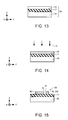
MEMS vibrator 300 according to the second modified example of the embodiment will be described with reference to the drawings.FIGS. 13 and 14 are cross-sectional views schematically showing manufacturing steps of theMEMS vibrator 300 according to the second modified example of the embodiment.FIGS. 13 and 14 correspond toFIG. 11 . - As shown in
FIG. 13 , an SOI (Silicon On Insulator)substrate 19 including thesubstrate 10, the insulatinglayer 17 formed on thesubstrate 10, and asilicon layer 18 formed on the insulatinglayer 17 is prepared. - As shown in
FIG. 14 , thesilicon layer 18 is doped with the predetermined impurity B. With this doping, thesilicon layer 18 can be converted to aconductive layer 28 provided with conductivity. - As shown in
FIG. 15 , theconductive layer 28 is patterned using a photolithographic technique and an etching technique to form thefirst electrode 20 and thesecond electrode 30 having the supportingportion 32 and thebeam portion 34. By the patterning, it is possible to form thefirst portion 36 whose length T in the Y-axis direction decreases toward thetip 35 of thebeam portion 34, and thesecond portion 38 whose length Tin the Y-axis direction is constant. Etching in the patterning may be performed using, for example, inductively coupled plasma reactive ion etching (ICP-RIE), or may be performed by the so-called Bosch process in which etching and etching sidewall passivation are repeated. When etching is performed by the Bosch process for example, isotropic etching is performed using sulfur hexafluoride (SF6) in an etching step, and the sidewall is passivated using a teflon (registered trademark) based gas (C4F8 or the like) in a passivation step, making it possible to suppress etching in the lateral direction (the X-axis direction and the Y-axis direction). - As shown in
FIGS. 11 and 12 , the insulatinglayer 17 is etched using thefirst electrode 20 and thesecond electrode 30 as masks. By the etching, the insulatinglayer 17 below thebeam portion 34 is removed. The insulatinglayer 17 below thefirst electrode 20 and the supportingportion 32 is not removed but side-etched in the illustrated example. Although not shown in the drawing, a through-hole penetrating from an upper face to a lower face of thebeam portion 34 may be formed for reliably removing the insulatinglayer 17 below thebeam portion 34. - Through the steps described above, the
MEMS vibrator 300 can be manufactured. - According to the manufacturing method of the
MEMS vibrator 300, thebeam portion 34 having thefirst portion 36 and thesecond portion 38 can be formed by patterning using a photolithographic technique and an etching technique. Accordingly, according to the manufacturing method of theMEMS vibrator 300, theMEMS vibrator 300 having high output and driven at a high frequency can be formed by a simple method compared to, for example, the manufacturing method of theMEMS vibrator 100. - Next, a MEMS vibrator according to a third modified example of the embodiment will be described with reference to the drawing.
FIG. 16 is a cross-sectional view schematically showing aMEMS vibrator 400 according to the third modified example of the embodiment, corresponding toFIG. 10 . Hereinafter, in theMEMS vibrator 400 according to the third modified example of the embodiment, members having functions similar to those of the constituent members of theMEMS vibrator 300 according to the second modified example of the embodiment are denoted by the same reference numerals and signs, and the detailed descriptions thereof are omitted. - In the example of the
MEMS vibrator 300 as shown inFIG. 10 , thebeam portion 34 has thesecond portion 38 whose length T in the Y-axis direction is constant. In contrast to this, in theMEMS vibrator 400 as shown inFIG. 16 , thebeam portion 34 does not have thesecond portion 38 but is composed of thefirst portion 36 whose length T in the Y-axis direction decreases toward thetip 35 of thebeam portion 34. - According to
MEMS vibrator 400, it is possible similarly to theMEMS vibrator 300 to reduce the mass of thebeam portion 34 without reducing the capacitance between thefirst electrode 20 and thebeam portion 34. Accordingly, theMEMS vibrator 400 has high output and can be driven at a high frequency. - A manufacturing method of the
MEMS vibrator 400 is basically the same as the manufacturing method of theMEMS vibrator 300. Accordingly, the description thereof is omitted. - Next, experimental examples of the MEMS vibrator according to the embodiment will be described with reference to the drawings. The invention is not limited at all by the following experimental examples.
- As the experimental examples, simulations in which the MEMS vibrator according to the embodiment is modeled were performed. In the simulations, frequencies were measured while changing the shape of a beam portion of a MEMS vibrator. The simulations were performed using I-DEAS (manufactured by Siemens PLM Software).
- In the simulations shown below, members having functions similar to those of the constituent members of the
MEMS vibrator 100 according to the embodiment are denoted by the same reference numerals and signs, and the detailed descriptions thereof are omitted. In the simulations shown below, a beam portion corresponds to the beam portion located in the region A overlapping the first electrode 20 (for example, refer toFIG. 1 ). In the simulations shown below, the Young's modulus of the beam portion is 123.2 GPa, and the density of the beam portion is 2230 kg/m3. -
FIG. 17 is a graph showing the results of a first simulation. In the first simulation, a frequency with respect to the length T of a tip of the beam portion in the normal-Q-direction was obtained. That is, inFIG. 17 , the plotted point (a) obtained when T=0 μm represents the value of a triangle-shapedbeam portion 34 as viewed from a direction perpendicular to the normal Q as shown inFIG. 18A . InFIG. 17 , the plotted point (b) obtained when T=1 μm represents the value of a trapezoid-shapedbeam portion 34 as shown inFIG. 18B . InFIG. 17 , the plotted point (c) obtained when T=2 μm represents the value of a rectangle-shaped beam portion 1034 (beam portion 1034 according to a comparative example) as shown inFIG. 18C . - Since the
first face 21 of thefirst electrode 20 and thesecond face 31 of thebeam portion 34 are parallel to each other (for example, refer toFIG. 1 ), the normal Q is illustrated as the normal of thesecond face 31 inFIGS. 18A and 18B . In the first simulation, the length L of the beam portion perpendicular to the normal Q is 10 μm, and the length (corresponding to W shown inFIG. 2 ) of the beam portion perpendicular to the directions of the normal Q and the length L is 2 μm. The same applies to a second simulation. - It is found from
FIG. 17 that the beam portions 34 (refer toFIGS. 18A and 18B ) whose lengths in the normal-Q-direction decrease toward thetip 35 are high in frequency compared to the rectangle-shaped beam portion 1034 (refer toFIG. 18C ). -
FIG. 19 is a graph showing the results of the second simulation. In the second simulation, a frequency with respect to the length L2 of a second portion (portion whose length in the normal-Q-direction is constant) of a beam portion in the direction perpendicular to the normal Q was obtained. That is, inFIG. 19 , the plotted point (d) obtained when L2=0 μm represents the value of a triangle-shapedbeam portion 34 as viewed from the direction perpendicular to the normal Q as shown inFIG. 20D . Thebeam portion 34 does not have thesecond portion 38 whose length in the normal-Q-direction is constant. InFIG. 19 , the plotted point (e) obtained when L2=3 μm represents the value of a trapezoid-shapedbeam portion 34 as shown inFIG. 20E . InFIG. 19 , the plotted point (f) obtained when L2=5 μm represents the value of a trapezoid-shapedbeam portion 34 as shown inFIG. 20F . InFIG. 19 , the plotted point (g) obtained when L2=10 μm represents the value of a rectangle-shaped beam portion 1034 (beam portion 1034 according to a comparative example) as shown inFIG. 20G . In the second simulation, the length of thesecond portion 38 in the normal-Q-direction is 2 μm. - It is found from
FIG. 19 that the beam portions 34 (refer toFIGS. 20D , 20E, and 20F) having thefirst portions 36 whose lengths in the normal-Q-direction decrease toward thetip 35 are high in frequency compared to the rectangle-shaped beam portion 1034 (refer toFIG. 20G ). - It is further found from
FIG. 19 that thebeam portions 34 having thesecond portions 38 whose lengths L2 fall within a range from 1 μm to 5 μm are high in frequency compared to thebeam portion 34 whose length L2=0 μm (that is, thebeam portion 34 without the second portion 38). In short, it is found that, by setting the value of L2 to L (L2/L) to from 1/10 to ½ (that is, by satisfying the expression (1)), driving at a higher frequency is possible. It is supposed that the frequency is increased by satisfying the expression (1) for the reason that, within the range of the expression (1), the spring constant can be assured to some extent while reducing the mass of thebeam portion 34. That is, it is supposed that, within the range of the expression (1), the balance between the mass and the spring constant is suitable for obtaining a high frequency. - The results of the first and second simulations do not depend on parameters such as the density or Young's modulus of the
beam portion 34, or the length of thesecond portion 38 in the normal-Q-direction, and are applicable. Even when these parameters change, the results indicate a similar tendency. Moreover, the results of the first and second simulations described above are not limited to the form in which, like theMEMS vibrator 100 for example, thebeam portion 34 vibrates in the direction parallel to the normal P of thesurface 11 of thesubstrate 10, but can be applied to the form in which, like theMEMS vibrator 300 for example, thebeam portion 34 vibrates in the direction perpendicular to the normal P. Even when the direction of vibration of thebeam portion 34 changes, the results indicate a similar tendency. - Next, an oscillator according to the embodiment will be described with reference to the drawing.
FIG. 21 schematically shows anoscillator 500 according to the embodiment. - As shown in
FIG. 21 , theoscillator 500 includes the MEMS vibrator (for example, the MEMS vibrator 100) according to the invention and anoscillator circuit 510. - The
oscillator circuit 510 is electrically connected to theMEMS vibrator 100. When a voltage is applied between theelectrodes MEMS vibrator 100 from theoscillator circuit 510, thebeam portion 34 can be vibrated by electrostatic force generated between theelectrodes MEMS vibrator 100 can oscillate at a resonant frequency with theoscillator circuit 510. - Transistors, capacitors (both not shown), and the like of which the
oscillator circuit 510 is composed may be formed on, for example, the supporting substrate 12 (refer toFIG. 1 ). With this configuration, theMEMS vibrator 100 and theoscillator circuit 510 can be formed monolithically. - When the
MEMS vibrator 100 and theoscillator circuit 510 are formed monolithically, members such as transistors of which theoscillator circuit 510 is composed may be formed in the same step as that of forming theMEMS vibrator 100 described above. Specifically, in the step of forming the sacrificial layer 40 (refer toFIG. 4 ), a gate insulating layer of the transistors may be formed. Further, in the step of forming the second electrode 30 (refer toFIG. 5 ), gate electrodes of the transistors may be formed. In this manner, the manufacturing steps are commonly used for theMEMS vibrator 100 and theoscillator circuit 510, whereby the manufacturing steps can be simplified. - According to the
oscillator 500, theMEMS vibrator 100 having high output and driven at a high frequency is included. Therefore, in theoscillator 500, the series resistance can be prevented from being increased, and the phase can be reversed. Accordingly, theoscillator 500 can satisfy oscillation conditions, and therefore can stably oscillate theMEMS vibrator 100 at a high frequency. - The embodiment and modified examples described above are illustrative only, and the invention is not limited to them. For example, it is also possible to appropriately combine the embodiment and the modified examples.
- While the embodiment of the invention has been described above in detail, those skilled in the art should readily understand that many modifications can be made without departing in substance from the novel matter and effects of the invention. Accordingly, all of those modified examples are deemed to be included in the scope of the invention.
- The entire disclosure of Japanese Patent Application No. 2011-075808, filed Mar. 30, 2011 is expressly incorporated by reference herein.
Claims (9)
1/10≦L 2 /L≦½ (1)
Applications Claiming Priority (2)
| Application Number | Priority Date | Filing Date | Title |
|---|---|---|---|
| JP2011-075808 | 2011-03-30 | ||
| JP2011075808A JP2012209885A (en) | 2011-03-30 | 2011-03-30 | Mems vibrator and oscillator |
Publications (2)
| Publication Number | Publication Date |
|---|---|
| US20120249253A1 true US20120249253A1 (en) | 2012-10-04 |
| US8847708B2 US8847708B2 (en) | 2014-09-30 |
Family
ID=46926430
Family Applications (1)
| Application Number | Title | Priority Date | Filing Date |
|---|---|---|---|
| US13/431,354 Expired - Fee Related US8847708B2 (en) | 2011-03-30 | 2012-03-27 | MEMS vibrator and oscillator |
Country Status (2)
| Country | Link |
|---|---|
| US (1) | US8847708B2 (en) |
| JP (1) | JP2012209885A (en) |
Cited By (3)
| Publication number | Priority date | Publication date | Assignee | Title |
|---|---|---|---|---|
| US20120146736A1 (en) * | 2010-12-13 | 2012-06-14 | Seiko Epson Corporation | Mems vibrator, oscillator, and method for manufacturing mems vibrator |
| US20140312734A1 (en) * | 2013-04-18 | 2014-10-23 | Seiko Epson Corporation | Vibrator, oscillator, electronic device, moving object, and method of manufacturing vibrator |
| US9233833B2 (en) | 2012-10-02 | 2016-01-12 | Seiko Epson Corporation | MEMS element and oscillator |
Families Citing this family (3)
| Publication number | Priority date | Publication date | Assignee | Title |
|---|---|---|---|---|
| JP2014116707A (en) * | 2012-12-07 | 2014-06-26 | Seiko Epson Corp | Method of manufacturing vibrator |
| JP6981040B2 (en) * | 2017-05-17 | 2021-12-15 | セイコーエプソン株式会社 | Encapsulation structures, electronic devices, electronic devices, and mobiles |
| KR102142056B1 (en) * | 2018-11-19 | 2020-08-06 | 전북대학교산학협력단 | Bulk acoustic wave resonator with tunable resonance characteristic and method thereof |
Citations (3)
| Publication number | Priority date | Publication date | Assignee | Title |
|---|---|---|---|---|
| US20030062961A1 (en) * | 2001-09-28 | 2003-04-03 | Qing Ma | Center-mass-reduced microbridge structures for ultra-high frequency MEM resonator |
| US20120146736A1 (en) * | 2010-12-13 | 2012-06-14 | Seiko Epson Corporation | Mems vibrator, oscillator, and method for manufacturing mems vibrator |
| US20130168782A1 (en) * | 2012-01-03 | 2013-07-04 | International Business Machines Corporation | Micro-electro-mechanical system (mems) structures and design structures |
Family Cites Families (7)
| Publication number | Priority date | Publication date | Assignee | Title |
|---|---|---|---|---|
| JP3553418B2 (en) | 1999-05-25 | 2004-08-11 | シャープ株式会社 | Vibration gyroscope, method of forming vibration gyroscope and adjustment method |
| EP1217735B1 (en) | 2000-12-21 | 2007-11-14 | ETA SA Manufacture Horlogère Suisse | Time base comprising an integrated micromechanical tuning fork resonator |
| JP2003133897A (en) | 2001-08-14 | 2003-05-09 | Seiko Epson Corp | Piezoelectric device, portable telephone device using piezoelectric device, and electronic device using piezoelectric device |
| EP1585219A1 (en) | 2004-04-06 | 2005-10-12 | Seiko Epson Corporation | A micro-flap type nano/micro mechanical device and fabrication method thereof |
| JP2006284551A (en) | 2005-02-23 | 2006-10-19 | Sony Corp | Vibration type gyro sensor |
| JP2007139505A (en) | 2005-11-16 | 2007-06-07 | Denso Corp | Capacitive mechanical quantity sensor |
| JP2010162629A (en) | 2009-01-14 | 2010-07-29 | Seiko Epson Corp | Method of manufacturing mems device |
-
2011
- 2011-03-30 JP JP2011075808A patent/JP2012209885A/en not_active Withdrawn
-
2012
- 2012-03-27 US US13/431,354 patent/US8847708B2/en not_active Expired - Fee Related
Patent Citations (4)
| Publication number | Priority date | Publication date | Assignee | Title |
|---|---|---|---|---|
| US20030062961A1 (en) * | 2001-09-28 | 2003-04-03 | Qing Ma | Center-mass-reduced microbridge structures for ultra-high frequency MEM resonator |
| US20120146736A1 (en) * | 2010-12-13 | 2012-06-14 | Seiko Epson Corporation | Mems vibrator, oscillator, and method for manufacturing mems vibrator |
| US8587390B2 (en) * | 2010-12-13 | 2013-11-19 | Seiko Epson Corporation | MEMS vibrator, oscillator, and method for manufacturing MEMS vibrator |
| US20130168782A1 (en) * | 2012-01-03 | 2013-07-04 | International Business Machines Corporation | Micro-electro-mechanical system (mems) structures and design structures |
Cited By (4)
| Publication number | Priority date | Publication date | Assignee | Title |
|---|---|---|---|---|
| US20120146736A1 (en) * | 2010-12-13 | 2012-06-14 | Seiko Epson Corporation | Mems vibrator, oscillator, and method for manufacturing mems vibrator |
| US8587390B2 (en) * | 2010-12-13 | 2013-11-19 | Seiko Epson Corporation | MEMS vibrator, oscillator, and method for manufacturing MEMS vibrator |
| US9233833B2 (en) | 2012-10-02 | 2016-01-12 | Seiko Epson Corporation | MEMS element and oscillator |
| US20140312734A1 (en) * | 2013-04-18 | 2014-10-23 | Seiko Epson Corporation | Vibrator, oscillator, electronic device, moving object, and method of manufacturing vibrator |
Also Published As
| Publication number | Publication date |
|---|---|
| US8847708B2 (en) | 2014-09-30 |
| JP2012209885A (en) | 2012-10-25 |
Similar Documents
| Publication | Publication Date | Title |
|---|---|---|
| US8289092B2 (en) | Microelectromechanical resonant structure having improved electrical characteristics | |
| US8847708B2 (en) | MEMS vibrator and oscillator | |
| CN101401303B (en) | MEMS resonator having at least one resonator mode shape and manufacturing method, oscillator and filter comprising the MEMS resonator | |
| US20100019869A1 (en) | Bulk mode resonator | |
| CN100568720C (en) | Torsional resonators and filters using them | |
| US8519806B2 (en) | Bulk-mode resonator having at least partially filled open cavities | |
| US8587390B2 (en) | MEMS vibrator, oscillator, and method for manufacturing MEMS vibrator | |
| JP2022529131A (en) | Micro electromechanical resonator | |
| US7579662B2 (en) | MEMS resonator and method of enhancing an output signal current from a MEMS resonator | |
| JP6060569B2 (en) | Manufacturing method of electronic device | |
| JP5225840B2 (en) | Vibrator, resonator using the same, and electromechanical filter using the same | |
| CN103663343A (en) | Electronic device, method of manufacturing the same, and oscillator | |
| JP4458081B2 (en) | Flap vibrator and integrated circuit including flap vibrator | |
| EP2755325B1 (en) | Resonant transducer and manufacturing method of resonant transducer | |
| JP5601463B2 (en) | MEMS vibrator, oscillator, and method for manufacturing MEMS vibrator | |
| JP2006263905A (en) | Micro electromechanical system having beam to be deformed by bending | |
| JP2013034156A (en) | Mems vibrator, oscillator and manufacturing method of mems vibrator | |
| US9233833B2 (en) | MEMS element and oscillator | |
| US8760234B2 (en) | MEMS vibrator and oscillator | |
| JP2013055647A (en) | Mems resonator and electrical device using the same | |
| JP5942582B2 (en) | Method for manufacturing vibrator | |
| JP2013038530A (en) | Mems vibrator and oscillator | |
| CN104868869A (en) | Vibrator, manufacturing method therefor, and electronic appliance | |
| JP2013106053A (en) | Mems vibrator, manufacturing method of the same and oscillator | |
| JP2013239895A (en) | Manufacturing method of vibrator |
Legal Events
| Date | Code | Title | Description |
|---|---|---|---|
| AS | Assignment |
Owner name: SEIKO EPSON CORPORATION, JAPAN Free format text: ASSIGNMENT OF ASSIGNORS INTEREST;ASSIGNOR:KIHARA, RYUJI;REEL/FRAME:027937/0445 Effective date: 20120315 |
|
| FEPP | Fee payment procedure |
Free format text: MAINTENANCE FEE REMINDER MAILED (ORIGINAL EVENT CODE: REM.) |
|
| LAPS | Lapse for failure to pay maintenance fees |
Free format text: PATENT EXPIRED FOR FAILURE TO PAY MAINTENANCE FEES (ORIGINAL EVENT CODE: EXP.); ENTITY STATUS OF PATENT OWNER: LARGE ENTITY |
|
| STCH | Information on status: patent discontinuation |
Free format text: PATENT EXPIRED DUE TO NONPAYMENT OF MAINTENANCE FEES UNDER 37 CFR 1.362 |
|
| FP | Expired due to failure to pay maintenance fee |
Effective date: 20180930 |