US20120249205A1 - Semiconductor Device, a Method of Improving a Distortion of an Output Waveform, and an Electronic Apparatus - Google Patents
Semiconductor Device, a Method of Improving a Distortion of an Output Waveform, and an Electronic Apparatus Download PDFInfo
- Publication number
- US20120249205A1 US20120249205A1 US13/432,097 US201213432097A US2012249205A1 US 20120249205 A1 US20120249205 A1 US 20120249205A1 US 201213432097 A US201213432097 A US 201213432097A US 2012249205 A1 US2012249205 A1 US 2012249205A1
- Authority
- US
- United States
- Prior art keywords
- clock signals
- time period
- clock signal
- delay time
- output
- Prior art date
- Legal status (The legal status is an assumption and is not a legal conclusion. Google has not performed a legal analysis and makes no representation as to the accuracy of the status listed.)
- Granted
Links
Images


Classifications
-
- H—ELECTRICITY
- H03—ELECTRONIC CIRCUITRY
- H03K—PULSE TECHNIQUE
- H03K5/00—Manipulating of pulses not covered by one of the other main groups of this subclass
- H03K5/15—Arrangements in which pulses are delivered at different times at several outputs, i.e. pulse distributors
- H03K5/15013—Arrangements in which pulses are delivered at different times at several outputs, i.e. pulse distributors with more than two outputs
- H03K5/1506—Arrangements in which pulses are delivered at different times at several outputs, i.e. pulse distributors with more than two outputs with parallel driven output stages; with synchronously driven series connected output stages
- H03K5/1508—Arrangements in which pulses are delivered at different times at several outputs, i.e. pulse distributors with more than two outputs with parallel driven output stages; with synchronously driven series connected output stages using a plurality of delay lines
-
- H—ELECTRICITY
- H03—ELECTRONIC CIRCUITRY
- H03K—PULSE TECHNIQUE
- H03K19/00—Logic circuits, i.e. having at least two inputs acting on one output; Inverting circuits
- H03K19/003—Modifications for increasing the reliability for protection
- H03K19/00369—Modifications for compensating variations of temperature, supply voltage or other physical parameters
Definitions
- the present invention relates to a semiconductor device, an electronic apparatus, and a method of improving an output waveform distortion.
- the semiconductor device inputs an input clock signal of a predetermined frequency and output a plurality of clock signals of the same frequency.
- Patent Literature 1 Japanese Patent Application Laying-Open Publication No. H06-28056
- Patent Literature 2 Japanese Patent Application Laying-Open Publication No. 2002-176343
- the present invention is achieved in order to solve the above-mentioned problems.
- the purpose of the present invention is to provide a semiconductor device, an electronic apparatus, and a method of improving an output waveform distortion each which can improve output waveform distortion of clock signals even with simple structure.
- One aspect of the present invention for achieving the above-mentioned purpose is to provide a semiconductor device comprising: an input unit configured to input an input clock signal of predetermined frequency; and a delay unit configured to generate a plurality of clock signals of the same frequency by providing predetermined delay time period to the input clock signal to be delayed in order to reduce load applied to a power supply in common with the plurality of the clock signals.
- Another aspect of the present invention is to provide a method of improving a distortion of an output waveform, the method comprising: inputting an input clock signal of predetermined frequency; and generating a plurality of clock signals of the same frequency by providing predetermined delay time period to the input clock signal to be delayed in order to reduce load applied to a power supply in common with the plurality of the clock signals.
- Still another aspect of the present invention is to provide an electronic apparatus comprising the aforementioned semiconductor device.
- the present invention can provide a semiconductor device, an electronic apparatus, and a method of improving an output waveform distortion each which can improve output waveform distortion of clock signals even with simple structure.
- FIG. 1 is an explanatory diagram of a conventional method of improving an output waveform distortion.
- FIG. 2 is an explanatory diagram of a conventional method of improving an output waveform distortion.
- FIG. 3 is a configuration diagram of a semiconductor device according to an embodiment of the present invention.
- FIG. 4 is a diagram showing a disposition example of a bypass capacitor according to the embodiment of the present invention.
- FIG. 5A is an explanatory diagram of delay time per one delay gate according to the embodiment of the present invention, and a diagram showing the case where one clock signal is output.
- FIG. 5B is an explanatory diagram of delay time per one delay gate according to the embodiment of the present invention, and a diagram showing the case where two clock signals are output.
- FIG. 5C is an explanatory diagram of delay time per one delay gate according to the embodiment of the present invention, and a diagram showing the case where three clock signals are output.
- FIG. 5D is an explanatory diagram of delay time per one delay gate according to the embodiment of the present invention, and a diagram showing the case where four clock signals are output.
- FIG. 6 is a diagram showing a simulation circuit according to the embodiment of the present invention.
- FIG. 7 is a diagram showing the simulation circuit according to the embodiment of the present invention.
- FIG. 8A is a diagram showing the case where the delay time period is 0 psec according to the embodiment of the present invention, and a diagram showing power supply potential.
- FIG. 8B is a diagram showing the case where the delay time period is 0 psec according to the embodiment of the present invention, and a diagram showing five normal clock signals.
- FIG. 8C is a diagram showing the case where the delay time period is 0 psec according to the embodiment of the present invention, and a diagram showing five inverted clock signals.
- FIG. 9A is a diagram showing the case where the delay time period is 100 psec according to the embodiment of the present invention, and a diagram showing power supply potential.
- FIG. 9B is a diagram showing the case where the delay time period is 100 psec according to the embodiment of the present invention, and a diagram showing five normal clock signals.
- FIG. 9C is a diagram showing the case where the delay time period is 100 psec according to the embodiment of the present invention, and a diagram showing five inverted clock signals.
- FIG. 10A is a diagram showing the case where the delay time period is 200 psec according to the embodiment of the present invention, and a diagram showing power supply potential.
- FIG. 10B is a diagram showing the case where the delay time period is 200 psec according to the embodiment of the present invention, and a diagram showing five normal clock signals.
- FIG. 10C is a diagram showing the case where the delay time period is 200 psec according to the embodiment of the present invention, and a diagram showing five inverted clock signals.
- FIG. 11A is a diagram showing the case where the delay time period is 300 psec according to the embodiment of the present invention, and a diagram showing power supply potential.
- FIG. 11B is a diagram showing the case where the delay time period is 300 psec according to the embodiment of the present invention, and a diagram showing five normal clock signals.
- FIG. 11C is a diagram showing the case where the delay time period is 300 psec according to the embodiment of the present invention, and a diagram showing five inverted clock signals.
- FIG. 12A is a diagram showing the case where the delay time period is 400 psec according to the embodiment of the present invention, and a diagram showing power supply potential.
- FIG. 12B is a diagram showing the case where the delay time period is 400 psec according to the embodiment of the present invention, and a diagram showing five normal clock signals.
- FIG. 12C is a diagram showing the case where the delay time period is 400 psec according to the embodiment of the present invention, and a diagram showing five inverted clock signals.
- FIG. 13A is a diagram showing the case where the delay time period is 500 psec according to the embodiment of the present invention, and a diagram showing power supply potential.
- FIG. 13B is a diagram showing the case where the delay time period is 500 psec according to the embodiment of the present invention, and a diagram showing five normal clock signals.
- FIG. 13C is a diagram showing the case where the delay time period is 500 psec according to the embodiment of the present invention, and a diagram showing five inverted clock signals.
- FIG. 14A is a diagram showing the case where the delay time period is 600 psec according to the embodiment of the present invention, and a diagram showing power supply potential.
- FIG. 14B is a diagram showing the case where the delay time period is 600 psec according to the embodiment of the present invention, and a diagram showing five normal clock signals.
- FIG. 14C is a diagram showing the case where the delay time period is 600 psec according to the embodiment of the present invention, and a diagram showing five inverted clock signals.
- FIG. 15A is a diagram showing the case where the delay time period is 700 psec according to the embodiment of the present invention, and a diagram showing power supply potential.
- FIG. 15B is a diagram showing the case where the delay time period is 700 psec according to the embodiment of the present invention, and a diagram showing five normal clock signals.
- FIG. 15C is a diagram showing the case where the delay time period is 700 psec according to the embodiment of the present invention, and a diagram showing five inverted clock signals.
- FIG. 16A is a diagram showing the case where the delay time period is 800 psec according to the embodiment of the present invention, and a diagram showing power supply potential.
- FIG. 16B is a diagram showing the case where the delay time period is 800 psec according to the embodiment of the present invention, and a diagram showing five normal clock signals.
- FIG. 16C is a diagram showing the case where the delay time period is 800 psec according to the embodiment of the present invention, and a diagram showing five inverted clock signals.
- FIG. 17A is a diagram showing the case where the delay time period is 900 psec according to the embodiment of the present invention, and a diagram showing power supply potential.
- FIG. 17B is a diagram showing the case where the delay time period is 900 psec according to the embodiment of the present invention, and a diagram showing five normal clock signals.
- FIG. 17C is a diagram showing the case where the delay time period is 900 psec according to the embodiment of the present invention, and a diagram showing five inverted clock signals.
- FIG. 18A is a diagram showing the case where the delay time period is 1000 psec according to the embodiment of the present invention, and a diagram showing power supply potential.
- FIG. 18B is a diagram showing the case where the delay time period is 1000 psec according to the embodiment of the present invention, and a diagram showing five normal clock signals.
- FIG. 18C is a diagram showing the case where the delay time period is 1000 psec according to the embodiment of the present invention, and a diagram showing five inverted clock signals.
- FIG. 19A is a diagram showing an alternative determining method of delay time according to the embodiment of the present invention, and is a schematic circuit diagram.
- FIG. 19B is a diagram showing the alternative determining method of delay time according to the embodiment of the present invention, and an explanatory diagram of time T 1 where the clock signal is turned to a high level from a low level.
- FIG. 19C is a diagram showing the alternative determining method of delay time according to embodiment of the present invention, and a diagram showing the case where three 100-MHz clock signals are outputted.
- FIG. 20 is a diagram showing an alternative disposition example of the bypass capacitor according to the embodiment of the present invention.
- FIG. 21 is a diagram showing a detailed disposition example of the bypass capacitor according to the embodiment of the present invention.
- FIG. 22A is a diagram showing an application example of the semiconductor device according to the embodiment of the present invention, and is a schematic front view diagram of a main unit of personal computer (PC).
- PC personal computer
- FIG. 22B is a diagram showing an application example of the semiconductor device according to the embodiment of the present invention, and is a schematic rear view diagram of the main unit of PC.
- FIG. 22C is a diagram showing an application example of the semiconductor device according to the embodiment of the present invention, and a schematic perspective diagram in the condition where a computer chassis of a side of the main unit of PC is removed.
- FIG. 22D is a diagram showing an application example of the semiconductor device according to the embodiment of the present invention, and a schematic top view diagram of a mother board mounted in the main unit of PC.
- FIG. 23 is a schematic block diagram of the mother board according to the embodiment of the present invention.
- FIG. 24A is a diagram showing an alternative application example of the semiconductor device according to the embodiment of the present invention, and a schematic front view diagram of a car-navigation system.
- FIG. 24B is a diagram showing the alternative application example of the semiconductor device according to the embodiment of the present invention, and a schematic front view diagram of a stand.
- FIG. 24C is a diagram showing the alternative application example of the semiconductor device according to the embodiment of the present invention, and is a schematic side view of the stand.
- FIG. 24D is a diagram showing the alternative application example of the semiconductor device according to the embodiment of the present invention, and is a schematic rear view diagram of the stand.
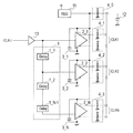
- FIG. 3 is a configuration diagram of a semiconductor device in an embodiment of the present invention.
- the semiconductor device is an apparatus which inputs an input clock signal CLK-I of predetermined frequency, and outputs N clock signals CLK 1 -CLKN of the same frequency, and adopts the following structure.
- a delay unit 1 provides predetermined delay time period in contrast to a plurality of clock signals in order to improve output waveform distortion of the clock signals. More specifically, It is composed of N- 1 delay gates 1 _ 1 , 1 _ 2 , . . . , 1 _N- 1 whose delay time period is the same, connected in a shape of cascade.
- the input clock signal CLK-I input from an input unit is input into the delay gate 1 _ 1 via a buffer 13 .
- An output from each delay gate 1 _ 1 , 1 _ 2 , . . . is input into each delay gate 1 _ 2 , 1 _ 3 , . . . in a subsequent stage, as clock signals CLK 2 , CLK 3 .
- each operational amplifier 2 _ 1 , 2 _ 2 , . . . , 2 _N outputs two differential clock pairs (i.e., a normal clock signal and an inverted clock signal) in which polarity is reversed from each output terminal.
- IO sections 4 _ 1 , 4 _ 2 , . . . , 4 _N for preventing an electrostatic discharge damage are disposed respectively in a subsequent stage of the operational amplifiers 2 _ 1 , 2 _ 2 , . . . , 2 _N. More specifically, the IO sections 4 _ 1 , 4 _ 2 , . . . , 4 _N are a diode between a clock line and a power supply, and a diode between a clock line and ground line (GND line).
- An IO section 4 _ 0 which is a protective element is disposed also at an output terminal of a regulator 11 .
- the operational amplifiers 2 _ 1 , 2 _ 2 , . . . , 2 _N and the IO sections 4 _ 1 , 4 _ 2 , . . . , 4 _N are collectively named “output IO” in some cases.
- bypass capacitors 3 _ 1 , 3 _ 2 , . . . , 3 _N are closely disposed for each output IO (the details are described later).
- FIG. 4 shows a detailed disposition example of the bypass capacitor 3 _ 1 .
- reference numeral 14 denotes P-channel MOS FET
- reference numeral 15 denotes N-channel MOS FET.
- a gate of the FET 14 is connected to a gate of the FET 15
- a drain of the FET 14 is connected to a drain of the FET 15 .
- a source of the FET 14 is connected to a power supply line (Vdd line) L 1 , and a source of the FET 15 is connected to a ground line (Vss line) L 2 .
- An inverter is composed of the FET 14 and the FET 15 .
- a first edge of the bypass capacitor 3 _ 1 is connected to the power supply line L 1 , and a second edge of the bypass capacitor 3 _ 1 is connected to the ground line L 2 .
- Capacity of the bypass capacitor 3 _ 1 can be determined arbitrarily.
- Other bypass capacitors 3 _ 2 , . . . , 3 _N are the same as that of the bypass capacitor 3 _ 1 .
- the regulator 11 shown in FIG. 3 is low drop out (LDO).
- a bypass capacitor 12 is disposed outside in order to keep voltage of the LDO constant to some extent.
- a parasitic coil component may exist in a wire connected to the output terminal. Since such as a coil component may act in a way to obstruct a fast component, the bypass capacitor is preferable to be disposed at a position in a minimum value of the coil component.
- the bypass capacitor is disposed between the power supply and the output IO, in a position near the output IO, as shown in FIG. 4 .
- the input clock signal CLK-I is input into the delay gate 1 _ 1 while being output from the output terminal as the clock signal CLK 1 of two differential clock pairs, without being delayed.
- the input clock signal CLK-I input into the delay gate 1 _ 1 is delayed with a predetermined time period (e.g., 1 psec) as a clock signal CLK 2 .
- the clock signal CLK 2 is delayed with the predetermined time period as compared with the clock signal CLK 1 .
- the clock signal CLK 2 produced in the delay gate 1 _ 1 is input into the delay gate 1 _ 2 while being output from the output terminal of the delay gate 1 _ 1 as the clock signal CLK 2 of two differential clock pairs.
- the clock signal CLK 2 input into the delay gate 1 _ 2 is further delayed with the predetermined time period as a clock signal CLK 3 .
- This clock signal CLK 3 is delayed with the predetermined time period as compared with the clock signal CLK 2 , and is delayed with two-fold predetermined time period as compared with the clock signal CLK 1 .
- the clock signal CLK 3 produced in the delay gate 1 _ 2 is input into the delay gate 1 _ 3 while being output from the output terminal of the delay gate 1 _ 2 as the clock signal CLK 3 of two differential clock pairs.
- the clock signal CLK 3 input into the delay gate 1 _ 3 is further delayed with the predetermined time period as a clock signal CLK 4 .
- the clock signal CLK 4 is delayed with predetermined time period as compared with the clock signal CLK 3 , is delayed with two-fold predetermined time period as compared with the clock signal CLK 2 , and is delayed with three-fold predetermined time period as compared with the clock signal CLK 1 .
- each clock signal CLK 4 , CLK 5 , . . . , CLKN- 1 is delayed sequentially in each of the delay gates 1 _ 4 to 1 _N- 1 at a subsequent stage. Accordingly, clock signals CLK 5 , CLK 6 , . . . , CLKN delayed with four-fold, five-fold, . . . , (N- 1 ) -fold predetermined time period as compared with the clock signal CLK 1 are output from each output terminal.
- the delay time period per one delay gate is preferable to be determined as 1 ⁇ 2N cycle period of the input clock signal CLK-I. That is, the delay time period of the clock signal CLK 1 of the first stage is set to 0, and each of the clock signals CLK 2 -CLKN of the second stage or later is delayed with each other by 1 ⁇ 2N cycle period of the input clock signal CLK-I.
- the aforementioned point will be explained in detail referring to FIG. 5 .
- FIG. 5A shows the case where one clock signal is output. In this case, since not to delay the clock signal, explanation is omitted.
- FIG. 5B shows the case where two clock signals are output.
- the clock signal of the second stage is delayed with 1/(2 ⁇ 2) cycle period (i.e., 1 ⁇ 4 cycle period) compared with the clock signal of the first stage. Accordingly, either of the clock signals rises or falls in the timing after 1 ⁇ 4 cycle period, 2/4 cycle period, 3 ⁇ 4 cycle period, . . . on the basis of the time point where the clock signal of the first stage rises.
- FIG. 5C shows the case where three clock signals are output.
- the clock signal of the second stage is delayed with 1/(2 ⁇ 3) cycle period (i.e., 1 ⁇ 6 cycle period) compared with the clock signal of the first stage.
- the clock signal of the third stage is delayed with 1 ⁇ 6 cycle period compared with the clock signal of the second stage.
- either of the clock signals rises or falls in the timing after 1 ⁇ 6 cycle period, 2/6 cycle period, 3/6 cycle period, . . . on the basis of the time point where the clock signal of the first stage rises.
- FIG. 5D shows the case where four clock signals are output.
- the clock signal of the second stage is delayed with 1/(2 ⁇ 4) cycle period (i.e., 1 ⁇ 8 cycle period) compared with the clock signal of the first stage.
- the clock signal of the third stage is delayed with 1 ⁇ 8 cycle period compared with the clock signal of the second stage.
- the clock signal of the fourth stage is delayed with 1 ⁇ 8 cycle period compared with the clock signal of the third stage. Accordingly, either of the clock signals rises or falls in the timing after 1 ⁇ 8 cycle period, 2/8 cycle period, 3 ⁇ 8, . . . cycle period on the basis of the time point where the clock signal of the first stage rises.
- the clock signals are delayed with each other by 1 ⁇ 2N cycle period, and thereby the timing of rising and falling of each clock signal can be dispersed equally. Therefore, load applied to a power supply is reduced, and thereby output waveform distortion of the clock signals can be improved.
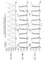
- FIG. 6 shows the case where the five normal clock signals out 1 -out 5 and five inverted clock signals out 1 b -out 5 b each having the same frequency (e.g., 100 MHz) are output, and all IO power supplies are supplied from an external power supply.
- the delay unit 1 As the delay unit 1 , as shown in left-hand of FIG. 6 , ideal power supplies disposed vertically to five stages are used.
- the circuit shown in FIG. 7 is corresponding to each operational amplifier 2 _ 1 , 2 _ 2 , . . . , 2 _N, and C 3 shown in the upper right of FIG. 7 is corresponding to each bypass capacitor 3 _ 1 , 3 _ 2 , . . . , 3 _N.
- FIG. 8 shows the case where the delay time period per one delay gate is set as 0 psec.
- FIG. 8A shows power supply potential
- FIG. 8B shows the five normal clock signals out 1 -out 5
- FIG. 8C shows five inverted clock signals out 1 b -out 5 b.
- FIG. 8B and FIG. 8C when the delay time period is 0 psec, the timing of rising and falling of each clock signal is aligned. Therefore, as shown in FIG. 8A , it proves that the power supply potential is varied largely.
- FIG. 9 shows the case where the delay time period is 100 psec.
- the delay time period is set to 100 psec, timing of rising and falling of each clock signal is delayed with each other by 100 psec. Accordingly, widths of the variations of the power supply potential are decreased even in small amount.
- the variations of the power supply potential were investigated, setting the delay time periods to be shifted to each other by 100 psec. Each result of measurement is shown in FIGS. 9-18 .
- the variations of the power supply potential are reduced as the delay time period is set to longer time periods, as shown in FIGS. 9-18 . Then, as shown in FIG. 18 , when the delay time period is 1000 psec, the power supply potential is almost fixed near 800 mV. Although not illustrated, when the delay time period is set to 1100 psec by adding further 100 psec, the variations of the power supply potential became larger, compared with the case where the delay time period is set to 1000 psec. That is, in the circuits as shown in FIG. 6 and FIG. 7 , if the delay time period per one delay gate is set as 1000 psec, the load applied to the power supply can be reduced extremely.
- N- 1 delay gates each whose delay time period is the same are connected in a shape of a cascade
- the present invention is not limited to the aforementioned structure. That is, the delay gates each whose delay time period differs from each other may be disposed in parallel. Alternatively, both of the structures maybe combined. Other delay elements can also be used instead of the delay gate.
- the predetermined delay time period is provided to the N clock signals, it is not necessary to provide the delay time period to the clock signal CLK 1 of the first stage, as described above. In this case, the predetermined delay time period can be considered to be 0.
- the similar delay time period as that of the clock signals CLK 2 -CLKN of the second stage or later can also be provided to the clock signal CLK 1 of the first stage.
- the delay time period per one delay gate is set as 1 ⁇ 2N cycle period of the input clock signal CLK-I, it is not necessary to satisfy the aforementioned conditions. That is, the delay time period can be modified suitably as required.
- FIG. 19 is a diagram showing an alternative determining method of the delay time.
- FIG. 19A shows an aspect that a clock IC (the semiconductor device) 20 outputs an input clock signal CLK-IN as a clock signal CLK_OUT, and the clock signal CLK_OUT is input into a device 30 which should be driven.
- a parasitic capacitor C 1 e.g. a printed circuit board (PCB) pattern
- PCB printed circuit board
- FIG. 19C shows the case of outputting three clock signals CLK_ 1 - 3 of 100 MHz (i.e., 10 nsec periods).
- time period to which the clock signals CLK_ 1 - 3 are turned from the low level to the high level is 1 nsec, it should just delay the clock signals CLK_ 1 - 3 with each other by 1 nsec.
- FIG. 20 is a diagram showing an alternative disposition example of the bypass capacitor in the embodiment of the present invention.
- a point that the bypass capacitors 3 _ 1 , 3 _ 2 , . . . , 3 _N are closely disposed for each output IO is as having already explained using FIG. 4 .
- the structure including the inverter is shown in FIG. 4 , but a structure including an operational amplifier 2 _ 1 is shown in FIG. 20 .
- a first edge of the operational amplifier 2 _ 1 is connected to a power supply line L 1
- a second edge of the operational amplifier 2 _ 1 is connected to a ground line L 2 .
- An IO section 4 _ 1 is disposed at the subsequent stage of the operational amplifier 2 _ 1 , and other devices are further connected via a PAD 5 _ 1 .
- a first edge of the bypass capacitor 3 _ 1 is connected to the power supply line L 1
- a second edge of the bypass capacitor 3 _ 1 is connected to the ground line L 2 .
- other bypass capacitors 3 _ 2 , . . . , 3 _N are the same as the bypass capacitor 3 _ 1 .
- FIG. 21 A detailed disposition example of such a bypass capacitor is shown in FIG. 21 .
- the reference numerals in FIG. 21 correspond to the reference numerals in FIG. 20 .
- the bypass capacitors 31 , 3 _ 2 , . . . , 3 _N are closely disposed for each output IO, in this embodiment.
- the phrase “being closely disposed” is corresponding that the value of the resistance between the output IO and the bypass capacitor is reduced.
- the value of the resistance between the output IO and the bypass capacitor can be reduced by making the wiring short or thick.
- FIG. 22 is a diagram showing an application example of the semiconductor device according to the embodiment of the present invention. More specifically, FIG. 22A shows a schematic front view diagram of a main unit of a personal computer (PC) 31 .
- FIG. 22B is a schematic rear view diagram of the main unit of PC 31 .
- FIG. 22C is a schematic perspective diagram in the condition of being removed a computer chassis of a side surface of the main unit of PC 31 .
- FIG. 22D is a schematic top view diagram of a mother board 32 mounted in the main unit of PC 31 .
- CPU 41 is connected to an IO chip 42 , an SD card 43 , a field programmable gate array (FPGA) 44 , and a PCI slot 45 and 46 , etc. using PCI Express, as shown by dotted-line arrows in FIG. 23 .
- FPGA field programmable gate array
- a network card, a SCSI card, a sound card, etc. are mounted on the PCI slots 45 and 46 .
- the clock generator 47 inputs the clock signal CLK_OUT, which is synchronized, into the various kinds of devices (e.g., the CPU 41 , the IO chip 42 , etc.), as shown by full-line arrows in FIG. 23 .
- the clock signal CLK_OUT in which output waveform distortion is improved, into the various kinds of devices (e.g., the CPU 41 , the IO chip 42 , etc.).
- FIG. 24 is a diagram showing an alternative application example of the semiconductor device according to the embodiment of the present invention. More specifically, FIG. 24A shows a schematic front view diagram of a car-navigation system 50 .
- the car-navigation system 50 includes a main unit 51 and required accessories 52 .
- the main unit 51 can be attached on a stand 53 .
- FIG. 24B is a schematic front view diagram of the stand 53
- FIG. 24C is a schematic side view of the stand 53
- FIG. 24D is a schematic rear view diagram of the stand 53 .
- the semiconductor device according to the embodiment is applicable also to a clock generator mounted in such a car-navigation system 50 .
- Detailed structure is the same as that of the PC 31 ( FIG. 23 ).
- the semiconductor device according to the embodiment can be applied to other electronic apparatus (e.g., a medical device, an entertainment device, an embedded system, etc.).
- the timing of rising and falling of each clock signal is dispersed by providing the predetermined delay time period to the plurality of the clock signals, and thereby the load applied to the power supply in common to the plurality of the clock signals can be reduced. That is, it is possible to improve the output waveform distortion of the clock signals even with simple structure, without providing an individual power supply for each output of the clock signals as conventional.
- the semiconductor device includes: the delay unit 1 which provides the predetermined delay time period for the plurality of the clock signals, and the output IO which outputs the plurality of the clock signals delayed in the delay unit 1 . Accordingly, it is possible to improve the output waveform distortion of the clock signals even with simple structure.
- the output IO includes the operational amplifiers 2 _ 1 , 2 _ 2 , . . . , 2 _N which output two differential clock pairs in which polarity is reversed. Accordingly, it is possible to output a normal clock signal and an inverted clock signal from each output terminal.
- the output IO may include an inverter which generates the clock signal as a single ended output (inverter output). That is, it is an available means not only to include the differential output, but to include the inverter output.
- the delay unit 1 delays each clock signal with each other by 1 ⁇ 2N cycle period of the input clock signal CLK-I. Accordingly, the timing of falling and rising of each clock signals can be dispersed equally.
- the N- 1 delay gates 1 _ 1 , 1 _ 2 , . . . , 1 _N- 1 each whose delay time period is the same is connected in a shape of a cascade, in the delay unit 1 . In such a manner, it is possible to provide the predetermined delay time period to N clock signals even with simple structure.
- the delay unit 1 includes the delay gates each whose delay time period differs from each other in parallel, when the number of the plurality of the clock signals is N. Accordingly, it is possible to provide the predetermined delay time period to N clock signals.
- the delay unit 1 provides the delay time period equivalent to the time period where the clock signal output from the output IO is turned from a low level to a high level (or from a high level to a low level). Accordingly, it is also possible to determine the delay time period in consideration of effect under the rise time and the fall time of the clock signals.
- bypass capacitors 3 _ 1 , 3 _ 2 , . . . , 3 _N are closely disposed for each output IO. Accordingly, it is possible to achieve a high speed response.
- a value of resistance between the output IO and the bypass capacitors 3 _ 1 , 3 _ 2 , . . . , 3 _N are reduced. Accordingly, if the bypass capacitors 3 _ 1 , 3 _ 2 , . . . , 3 _N are closely disposed for each output IO, the effect can be enhanced.
- the present invention is not only achievable as the semiconductor device, but also achievable as a method of improving the output waveform distortion including a step(s) to which a characteristic process of such a semiconductor device is realized.
- the present invention is also achievable as a computer program for making a computer execute the step(s). It needless to say that such a program can be distributed via recording media (e.g., CD-ROM) and/or transmission media (e.g., Internet).
- the semiconductor device and the method of improving the output waveform distortion according to the present invention are applicable to an electronic apparatus with required outputting a plurality of clock signals of the same frequency. More specifically, the semiconductor device and the method of improving the output waveform distortion according to the present invention is applicable to a personal computer, a car-navigation system, a medical device, an entertainment device, an embedded system, or the like.
Landscapes
- Physics & Mathematics (AREA)
- Engineering & Computer Science (AREA)
- Computer Hardware Design (AREA)
- Computing Systems (AREA)
- General Engineering & Computer Science (AREA)
- Mathematical Physics (AREA)
- Nonlinear Science (AREA)
- Manipulation Of Pulses (AREA)
- Pulse Circuits (AREA)
- Semiconductor Integrated Circuits (AREA)
- Logic Circuits (AREA)
- Design And Manufacture Of Integrated Circuits (AREA)
Abstract
Description
- This application is based upon and claims the benefit of priority from prior Japanese Patent Application Nos. P2011-79225 filed on Mar. 31, 2011, and P2012-041347 filed on Feb. 28, 2012, the entire contents of which are incorporated herein by reference.
- The present invention relates to a semiconductor device, an electronic apparatus, and a method of improving an output waveform distortion. The semiconductor device inputs an input clock signal of a predetermined frequency and output a plurality of clock signals of the same frequency.
- Generally, since a plurality of clock signals are required for an electronic apparatus, an apparatus which outputs a plurality of clock signals of the same frequency is known (Refer to
Patent Literatures 1 and 2). However, if a plurality of clock signals of precisely same frequency is output simultaneously, load applied to a power supply will be increased, thereby becoming a factor in which an output waveform of the clock signals is distorted. Thus, it has been known about a method of including a power supply for each output of clock signal as shown inFIG. 1 , a method of building a regulator for each output of clock signal as indicated inFIG. 2 , etc. According to the above-mentioned methods, since an individual power supply is included in each output of clock signal, an output waveform distortion of the clock signals can be improved. - Patent Literature 1: Japanese Patent Application Laying-Open Publication No. H06-28056
- Patent Literature 2: Japanese Patent Application Laying-Open Publication No. 2002-176343
- However, although output waveform distortion of clock signals can be improved, it was hard to adopt actually the above-mentioned conventional technologies. For example, the method of including the individual power supply for each output of clock signals is not adoptable if there is no remainder of the number of pins of the power supply. On the other hand, since a circuit area becomes wide according to the method of building the regulator for each output of clock signals, there is a problem that the cost will be increased.
- The present invention is achieved in order to solve the above-mentioned problems. The purpose of the present invention is to provide a semiconductor device, an electronic apparatus, and a method of improving an output waveform distortion each which can improve output waveform distortion of clock signals even with simple structure.
- One aspect of the present invention for achieving the above-mentioned purpose is to provide a semiconductor device comprising: an input unit configured to input an input clock signal of predetermined frequency; and a delay unit configured to generate a plurality of clock signals of the same frequency by providing predetermined delay time period to the input clock signal to be delayed in order to reduce load applied to a power supply in common with the plurality of the clock signals.
- Another aspect of the present invention is to provide a method of improving a distortion of an output waveform, the method comprising: inputting an input clock signal of predetermined frequency; and generating a plurality of clock signals of the same frequency by providing predetermined delay time period to the input clock signal to be delayed in order to reduce load applied to a power supply in common with the plurality of the clock signals.
- Still another aspect of the present invention is to provide an electronic apparatus comprising the aforementioned semiconductor device.
- According to the present invention, it can provide a semiconductor device, an electronic apparatus, and a method of improving an output waveform distortion each which can improve output waveform distortion of clock signals even with simple structure.
-
FIG. 1 is an explanatory diagram of a conventional method of improving an output waveform distortion. -
FIG. 2 is an explanatory diagram of a conventional method of improving an output waveform distortion. -
FIG. 3 is a configuration diagram of a semiconductor device according to an embodiment of the present invention. -
FIG. 4 is a diagram showing a disposition example of a bypass capacitor according to the embodiment of the present invention. -
FIG. 5A is an explanatory diagram of delay time per one delay gate according to the embodiment of the present invention, and a diagram showing the case where one clock signal is output. -
FIG. 5B is an explanatory diagram of delay time per one delay gate according to the embodiment of the present invention, and a diagram showing the case where two clock signals are output. -
FIG. 5C is an explanatory diagram of delay time per one delay gate according to the embodiment of the present invention, and a diagram showing the case where three clock signals are output. -
FIG. 5D is an explanatory diagram of delay time per one delay gate according to the embodiment of the present invention, and a diagram showing the case where four clock signals are output. -
FIG. 6 is a diagram showing a simulation circuit according to the embodiment of the present invention. -
FIG. 7 is a diagram showing the simulation circuit according to the embodiment of the present invention. -
FIG. 8A is a diagram showing the case where the delay time period is 0 psec according to the embodiment of the present invention, and a diagram showing power supply potential. -
FIG. 8B is a diagram showing the case where the delay time period is 0 psec according to the embodiment of the present invention, and a diagram showing five normal clock signals. -
FIG. 8C is a diagram showing the case where the delay time period is 0 psec according to the embodiment of the present invention, and a diagram showing five inverted clock signals. -
FIG. 9A is a diagram showing the case where the delay time period is 100 psec according to the embodiment of the present invention, and a diagram showing power supply potential. -
FIG. 9B is a diagram showing the case where the delay time period is 100 psec according to the embodiment of the present invention, and a diagram showing five normal clock signals. -
FIG. 9C is a diagram showing the case where the delay time period is 100 psec according to the embodiment of the present invention, and a diagram showing five inverted clock signals. -
FIG. 10A is a diagram showing the case where the delay time period is 200 psec according to the embodiment of the present invention, and a diagram showing power supply potential. -
FIG. 10B is a diagram showing the case where the delay time period is 200 psec according to the embodiment of the present invention, and a diagram showing five normal clock signals. -
FIG. 10C is a diagram showing the case where the delay time period is 200 psec according to the embodiment of the present invention, and a diagram showing five inverted clock signals. -
FIG. 11A is a diagram showing the case where the delay time period is 300 psec according to the embodiment of the present invention, and a diagram showing power supply potential. -
FIG. 11B is a diagram showing the case where the delay time period is 300 psec according to the embodiment of the present invention, and a diagram showing five normal clock signals. -
FIG. 11C is a diagram showing the case where the delay time period is 300 psec according to the embodiment of the present invention, and a diagram showing five inverted clock signals. -
FIG. 12A is a diagram showing the case where the delay time period is 400 psec according to the embodiment of the present invention, and a diagram showing power supply potential. -
FIG. 12B is a diagram showing the case where the delay time period is 400 psec according to the embodiment of the present invention, and a diagram showing five normal clock signals. -
FIG. 12C is a diagram showing the case where the delay time period is 400 psec according to the embodiment of the present invention, and a diagram showing five inverted clock signals. -
FIG. 13A is a diagram showing the case where the delay time period is 500 psec according to the embodiment of the present invention, and a diagram showing power supply potential. -
FIG. 13B is a diagram showing the case where the delay time period is 500 psec according to the embodiment of the present invention, and a diagram showing five normal clock signals. -
FIG. 13C is a diagram showing the case where the delay time period is 500 psec according to the embodiment of the present invention, and a diagram showing five inverted clock signals. -
FIG. 14A is a diagram showing the case where the delay time period is 600 psec according to the embodiment of the present invention, and a diagram showing power supply potential. -
FIG. 14B is a diagram showing the case where the delay time period is 600 psec according to the embodiment of the present invention, and a diagram showing five normal clock signals. -
FIG. 14C is a diagram showing the case where the delay time period is 600 psec according to the embodiment of the present invention, and a diagram showing five inverted clock signals. -
FIG. 15A is a diagram showing the case where the delay time period is 700 psec according to the embodiment of the present invention, and a diagram showing power supply potential. -
FIG. 15B is a diagram showing the case where the delay time period is 700 psec according to the embodiment of the present invention, and a diagram showing five normal clock signals. -
FIG. 15C is a diagram showing the case where the delay time period is 700 psec according to the embodiment of the present invention, and a diagram showing five inverted clock signals. -
FIG. 16A is a diagram showing the case where the delay time period is 800 psec according to the embodiment of the present invention, and a diagram showing power supply potential. -
FIG. 16B is a diagram showing the case where the delay time period is 800 psec according to the embodiment of the present invention, and a diagram showing five normal clock signals. -
FIG. 16C is a diagram showing the case where the delay time period is 800 psec according to the embodiment of the present invention, and a diagram showing five inverted clock signals. -
FIG. 17A is a diagram showing the case where the delay time period is 900 psec according to the embodiment of the present invention, and a diagram showing power supply potential. -
FIG. 17B is a diagram showing the case where the delay time period is 900 psec according to the embodiment of the present invention, and a diagram showing five normal clock signals. -
FIG. 17C is a diagram showing the case where the delay time period is 900 psec according to the embodiment of the present invention, and a diagram showing five inverted clock signals. -
FIG. 18A is a diagram showing the case where the delay time period is 1000 psec according to the embodiment of the present invention, and a diagram showing power supply potential. -
FIG. 18B is a diagram showing the case where the delay time period is 1000 psec according to the embodiment of the present invention, and a diagram showing five normal clock signals. -
FIG. 18C is a diagram showing the case where the delay time period is 1000 psec according to the embodiment of the present invention, and a diagram showing five inverted clock signals. -
FIG. 19A is a diagram showing an alternative determining method of delay time according to the embodiment of the present invention, and is a schematic circuit diagram. -
FIG. 19B is a diagram showing the alternative determining method of delay time according to the embodiment of the present invention, and an explanatory diagram of time T1 where the clock signal is turned to a high level from a low level. -
FIG. 19C is a diagram showing the alternative determining method of delay time according to embodiment of the present invention, and a diagram showing the case where three 100-MHz clock signals are outputted. -
FIG. 20 is a diagram showing an alternative disposition example of the bypass capacitor according to the embodiment of the present invention. -
FIG. 21 is a diagram showing a detailed disposition example of the bypass capacitor according to the embodiment of the present invention. -
FIG. 22A is a diagram showing an application example of the semiconductor device according to the embodiment of the present invention, and is a schematic front view diagram of a main unit of personal computer (PC). -
FIG. 22B is a diagram showing an application example of the semiconductor device according to the embodiment of the present invention, and is a schematic rear view diagram of the main unit of PC. -
FIG. 22C is a diagram showing an application example of the semiconductor device according to the embodiment of the present invention, and a schematic perspective diagram in the condition where a computer chassis of a side of the main unit of PC is removed. -
FIG. 22D is a diagram showing an application example of the semiconductor device according to the embodiment of the present invention, and a schematic top view diagram of a mother board mounted in the main unit of PC. -
FIG. 23 is a schematic block diagram of the mother board according to the embodiment of the present invention. -
FIG. 24A is a diagram showing an alternative application example of the semiconductor device according to the embodiment of the present invention, and a schematic front view diagram of a car-navigation system. -
FIG. 24B is a diagram showing the alternative application example of the semiconductor device according to the embodiment of the present invention, and a schematic front view diagram of a stand. -
FIG. 24C is a diagram showing the alternative application example of the semiconductor device according to the embodiment of the present invention, and is a schematic side view of the stand. -
FIG. 24D is a diagram showing the alternative application example of the semiconductor device according to the embodiment of the present invention, and is a schematic rear view diagram of the stand. - Next, certain embodiments of the invention will be described with reference to drawings. In the description of the following drawings, the identical or similar reference numeral is attached to the identical or similar part. However, it should be known about that the drawings are schematic and the relation between thickness and the plane size and the ratio of the thickness of each layer differs from an actual thing. Therefore, detailed thickness and size should be determined in consideration of the following explanation. Of course, the part from which the relation and ratio of a mutual size differ also in mutually drawings is included.
- Moreover, the embodiments shown hereinafter exemplify the apparatus and method for materializing the technical idea of the present invention; and the embodiments of the present invention does not specify the material, shape, structure, placement, etc. of component parts as the following. Various changes can be added to the technical idea of the present invention in scope of claims.
- Hereinafter, an embodiment of the present invention will be described in detail with reference to drawings.
-
FIG. 3 is a configuration diagram of a semiconductor device in an embodiment of the present invention. As shown inFIG. 3 , the semiconductor device is an apparatus which inputs an input clock signal CLK-I of predetermined frequency, and outputs N clock signals CLK1-CLKN of the same frequency, and adopts the following structure. - Firstly, a
delay unit 1 provides predetermined delay time period in contrast to a plurality of clock signals in order to improve output waveform distortion of the clock signals. More specifically, It is composed of N-1 delay gates 1_1, 1_2, . . . , 1_N-1 whose delay time period is the same, connected in a shape of cascade. - The input clock signal CLK-I input from an input unit is input into the delay gate 1_1 via a
buffer 13. An output from each delay gate 1_1, 1_2, . . . is input into each delay gate 1_2, 1_3, . . . in a subsequent stage, as clock signals CLK2, CLK3. - The input clock signal CLK-I and the clock signals
- CLK2-CLKN are input into each operational amplifier 2_1, 2_2, . . . , 2_N. Accordingly, each operational amplifier 2_1, 2_2, . . . , 2_N outputs two differential clock pairs (i.e., a normal clock signal and an inverted clock signal) in which polarity is reversed from each output terminal.
- IO sections 4_1, 4_2, . . . , 4_N for preventing an electrostatic discharge damage are disposed respectively in a subsequent stage of the operational amplifiers 2_1, 2_2, . . . , 2_N. More specifically, the IO sections 4_1, 4_2, . . . , 4_N are a diode between a clock line and a power supply, and a diode between a clock line and ground line (GND line). An IO section 4_0 which is a protective element is disposed also at an output terminal of a
regulator 11. In the following explanation, the operational amplifiers 2_1, 2_2, . . . , 2_N and the IO sections 4_1, 4_2, . . . , 4_N are collectively named “output IO” in some cases. - According to the embodiment, as shown in
FIG. 3 , bypass capacitors 3_1, 3_2, . . . , 3_N are closely disposed for each output IO (the details are described later).FIG. 4 shows a detailed disposition example of the bypass capacitor 3_1. InFIG. 4 ,reference numeral 14 denotes P-channel MOS FET, andreference numeral 15 denotes N-channel MOS FET. A gate of theFET 14 is connected to a gate of theFET 15, and a drain of theFET 14 is connected to a drain of theFET 15. A source of theFET 14 is connected to a power supply line (Vdd line) L1, and a source of theFET 15 is connected to a ground line (Vss line) L2. An inverter is composed of theFET 14 and theFET 15. A first edge of the bypass capacitor 3_1 is connected to the power supply line L1, and a second edge of the bypass capacitor 3_1 is connected to the ground line L2. Capacity of the bypass capacitor 3_1 can be determined arbitrarily. Other bypass capacitors 3_2, . . . , 3_N are the same as that of the bypass capacitor 3_1. - Specifically, the
regulator 11 shown inFIG. 3 is low drop out (LDO). Abypass capacitor 12 is disposed outside in order to keep voltage of the LDO constant to some extent. A parasitic coil component may exist in a wire connected to the output terminal. Since such as a coil component may act in a way to obstruct a fast component, the bypass capacitor is preferable to be disposed at a position in a minimum value of the coil component. Thus, in the embodiment, the bypass capacitor is disposed between the power supply and the output IO, in a position near the output IO, as shown inFIG. 4 . - Hereinafter, an operation example at the time where such a semiconductor device delays a clock signal will be explained in detail.
- Firstly, the input clock signal CLK-I is input into the delay gate 1_1 while being output from the output terminal as the clock signal CLK1 of two differential clock pairs, without being delayed. The input clock signal CLK-I input into the delay gate 1_1 is delayed with a predetermined time period (e.g., 1 psec) as a clock signal CLK2. The clock signal CLK2 is delayed with the predetermined time period as compared with the clock signal CLK1.
- Subsequently, the clock signal CLK2 produced in the delay gate 1_1 is input into the delay gate 1_2 while being output from the output terminal of the delay gate 1_1 as the clock signal CLK2 of two differential clock pairs. The clock signal CLK2 input into the delay gate 1_2 is further delayed with the predetermined time period as a clock signal CLK3. This clock signal CLK3 is delayed with the predetermined time period as compared with the clock signal CLK2, and is delayed with two-fold predetermined time period as compared with the clock signal CLK1.
- Subsequently, the clock signal CLK3 produced in the delay gate 1_2 is input into the delay gate 1_3 while being output from the output terminal of the delay gate 1_2 as the clock signal CLK3 of two differential clock pairs. The clock signal CLK3 input into the delay gate 1_3 is further delayed with the predetermined time period as a clock signal CLK4. The clock signal CLK4 is delayed with predetermined time period as compared with the clock signal CLK3, is delayed with two-fold predetermined time period as compared with the clock signal CLK2, and is delayed with three-fold predetermined time period as compared with the clock signal CLK1.
- From then on, each clock signal CLK4, CLK5, . . . , CLKN-1 is delayed sequentially in each of the delay gates 1_4 to 1_N-1 at a subsequent stage. Accordingly, clock signals CLK5, CLK6, . . . , CLKN delayed with four-fold, five-fold, . . . , (N-1) -fold predetermined time period as compared with the clock signal CLK1 are output from each output terminal.
- Next, a determining method of delay time will be explained. When outputting N clock signals CLK1-CLKN, the delay time period per one delay gate is preferable to be determined as ½N cycle period of the input clock signal CLK-I. That is, the delay time period of the clock signal CLK1 of the first stage is set to 0, and each of the clock signals CLK2-CLKN of the second stage or later is delayed with each other by ½N cycle period of the input clock signal CLK-I. Hereinafter, the aforementioned point will be explained in detail referring to
FIG. 5 . -
FIG. 5A shows the case where one clock signal is output. In this case, since not to delay the clock signal, explanation is omitted. -
FIG. 5B shows the case where two clock signals are output. As shown inFIG. 5B , when outputting two clock signals, the clock signal of the second stage is delayed with 1/(2×2) cycle period (i.e., ¼ cycle period) compared with the clock signal of the first stage. Accordingly, either of the clock signals rises or falls in the timing after ¼ cycle period, 2/4 cycle period, ¾ cycle period, . . . on the basis of the time point where the clock signal of the first stage rises. -
FIG. 5C shows the case where three clock signals are output. As shown inFIG. 5C , when outputting three clock signals, the clock signal of the second stage is delayed with 1/(2×3) cycle period (i.e., ⅙ cycle period) compared with the clock signal of the first stage. Similarly, the clock signal of the third stage is delayed with ⅙ cycle period compared with the clock signal of the second stage. - Accordingly, either of the clock signals rises or falls in the timing after ⅙ cycle period, 2/6 cycle period, 3/6 cycle period, . . . on the basis of the time point where the clock signal of the first stage rises.
-
FIG. 5D shows the case where four clock signals are output. As shown inFIG. 5D , when outputting four clock signals, the clock signal of the second stage is delayed with 1/(2×4) cycle period (i.e., ⅛ cycle period) compared with the clock signal of the first stage. Similarly, the clock signal of the third stage is delayed with ⅛ cycle period compared with the clock signal of the second stage. Furthermore, the clock signal of the fourth stage is delayed with ⅛ cycle period compared with the clock signal of the third stage. Accordingly, either of the clock signals rises or falls in the timing after ⅛ cycle period, 2/8 cycle period, ⅜, . . . cycle period on the basis of the time point where the clock signal of the first stage rises. - Thus, the clock signals are delayed with each other by ½N cycle period, and thereby the timing of rising and falling of each clock signal can be dispersed equally. Therefore, load applied to a power supply is reduced, and thereby output waveform distortion of the clock signals can be improved.
- Next, a result of a simulation will be explained. Here, since to investigate a delay time period which reduces the load applied to the power supply extremely, the simulation was performed using circuits shown in
FIG. 6 andFIG. 7 . That is,FIG. 6 shows the case where the five normal clock signals out1-out5 and five inverted clock signals out1 b-out5 b each having the same frequency (e.g., 100 MHz) are output, and all IO power supplies are supplied from an external power supply. As thedelay unit 1, as shown in left-hand ofFIG. 6 , ideal power supplies disposed vertically to five stages are used. The circuit shown inFIG. 7 is corresponding to each operational amplifier 2_1, 2_2, . . . , 2_N, and C3 shown in the upper right ofFIG. 7 is corresponding to each bypass capacitor 3_1, 3_2, . . . , 3_N. -
FIG. 8 shows the case where the delay time period per one delay gate is set as 0 psec.FIG. 8A shows power supply potential,FIG. 8B shows the five normal clock signals out1-out5, andFIG. 8C shows five inverted clock signals out1 b-out5 b. As shown inFIG. 8B andFIG. 8C , when the delay time period is 0 psec, the timing of rising and falling of each clock signal is aligned. Therefore, as shown inFIG. 8A , it proves that the power supply potential is varied largely. -
FIG. 9 shows the case where the delay time period is 100 psec. As shown inFIG. 9 , when the delay time period is set to 100 psec, timing of rising and falling of each clock signal is delayed with each other by 100 psec. Accordingly, widths of the variations of the power supply potential are decreased even in small amount. Hereinafter, the variations of the power supply potential were investigated, setting the delay time periods to be shifted to each other by 100 psec. Each result of measurement is shown inFIGS. 9-18 . - The variations of the power supply potential are reduced as the delay time period is set to longer time periods, as shown in
FIGS. 9-18 . Then, as shown inFIG. 18 , when the delay time period is 1000 psec, the power supply potential is almost fixed near 800 mV. Although not illustrated, when the delay time period is set to 1100 psec by adding further 100 psec, the variations of the power supply potential became larger, compared with the case where the delay time period is set to 1000 psec. That is, in the circuits as shown inFIG. 6 andFIG. 7 , if the delay time period per one delay gate is set as 1000 psec, the load applied to the power supply can be reduced extremely. - In this case, although N-1 delay gates each whose delay time period is the same are connected in a shape of a cascade, the present invention is not limited to the aforementioned structure. That is, the delay gates each whose delay time period differs from each other may be disposed in parallel. Alternatively, both of the structures maybe combined. Other delay elements can also be used instead of the delay gate.
- Moreover, in this case, although the predetermined delay time period is provided to the N clock signals, it is not necessary to provide the delay time period to the clock signal CLK1 of the first stage, as described above. In this case, the predetermined delay time period can be considered to be 0. Of course, the similar delay time period as that of the clock signals CLK2-CLKN of the second stage or later can also be provided to the clock signal CLK1 of the first stage.
- Moreover, although the delay time period per one delay gate is set as ½N cycle period of the input clock signal CLK-I, it is not necessary to satisfy the aforementioned conditions. That is, the delay time period can be modified suitably as required.
-
FIG. 19 is a diagram showing an alternative determining method of the delay time. Here,FIG. 19A shows an aspect that a clock IC (the semiconductor device) 20 outputs an input clock signal CLK-IN as a clock signal CLK_OUT, and the clock signal CLK_OUT is input into adevice 30 which should be driven. In this case, a parasitic capacitor C1 (e.g. a printed circuit board (PCB) pattern) is disposed between theclock IC 20 and thedevice 30, and there is also a gate capacitance C2 in thedevice 30. Therefore, as shown in T1 ofFIG. 19B , the load applied to the power supply becomes heavy due to electric charging from Vdd to the parasitic capacitor C1 etc. Such a tendency is remarkable as the parasitic capacitor C1 etc. becomes large, as a dotted line shown inFIG. 19B . Accordingly, it should just provide a delay time period equivalent to the time period T1 where the clock signal CLK_OUT is turned from a low level to a high level (or from a high level to a low level). For example,FIG. 19C shows the case of outputting three clock signals CLK_1-3 of 100 MHz (i.e., 10 nsec periods). In this case, since time period to which the clock signals CLK_1-3 are turned from the low level to the high level is 1 nsec, it should just delay the clock signals CLK_1-3 with each other by 1 nsec. Thus, it is also possible to determine the delay time period in consideration of effect under the rise time and the fall time of the clock signals. -
FIG. 20 is a diagram showing an alternative disposition example of the bypass capacitor in the embodiment of the present invention. A point that the bypass capacitors 3_1, 3_2, . . . , 3_N are closely disposed for each output IO is as having already explained usingFIG. 4 . The structure including the inverter is shown inFIG. 4 , but a structure including an operational amplifier 2_1 is shown inFIG. 20 . A first edge of the operational amplifier 2_1 is connected to a power supply line L1, and a second edge of the operational amplifier 2_1 is connected to a ground line L2. An IO section 4_1 is disposed at the subsequent stage of the operational amplifier 2_1, and other devices are further connected via a PAD 5_1. A first edge of the bypass capacitor 3_1 is connected to the power supply line L1, and a second edge of the bypass capacitor 3_1 is connected to the ground line L2. Here, although the explanation is given with focus of attention on the bypass capacitor 3_1, of course, other bypass capacitors 3_2, . . . , 3_N are the same as the bypass capacitor 3_1. A detailed disposition example of such a bypass capacitor is shown inFIG. 21 . Of course, the reference numerals inFIG. 21 correspond to the reference numerals inFIG. 20 . - As already explained, the
bypass capacitors 31, 3_2, . . . , 3_N are closely disposed for each output IO, in this embodiment. The phrase “being closely disposed” is corresponding that the value of the resistance between the output IO and the bypass capacitor is reduced. For example, the value of the resistance between the output IO and the bypass capacitor can be reduced by making the wiring short or thick. -
FIG. 22 is a diagram showing an application example of the semiconductor device according to the embodiment of the present invention. More specifically,FIG. 22A shows a schematic front view diagram of a main unit of a personal computer (PC) 31.FIG. 22B is a schematic rear view diagram of the main unit ofPC 31.FIG. 22C is a schematic perspective diagram in the condition of being removed a computer chassis of a side surface of the main unit ofPC 31.FIG. 22D is a schematic top view diagram of amother board 32 mounted in the main unit ofPC 31. - Various kinds of devices (e.g., CPU, a clock generator, etc.) are mounted on the
mother board 32. The semiconductor device according to the embodiment is applicable to the clock generator mounted on themother board 32. That is,CPU 41 is connected to anIO chip 42, anSD card 43, a field programmable gate array (FPGA) 44, and aPCI slot FIG. 23 . A network card, a SCSI card, a sound card, etc. are mounted on thePCI slots CPU 41, theIO chip 42, etc.). That is, theclock generator 47 inputs the clock signal CLK_OUT, which is synchronized, into the various kinds of devices (e.g., theCPU 41, theIO chip 42, etc.), as shown by full-line arrows inFIG. 23 . In accordance with the semiconductor device according to the embodiment applied to such aclock generator 47, it is possible to input the clock signal CLK_OUT, in which output waveform distortion is improved, into the various kinds of devices (e.g., theCPU 41, theIO chip 42, etc.). -
FIG. 24 is a diagram showing an alternative application example of the semiconductor device according to the embodiment of the present invention. More specifically,FIG. 24A shows a schematic front view diagram of a car-navigation system 50. The car-navigation system 50 includes amain unit 51 and requiredaccessories 52. Themain unit 51 can be attached on astand 53.FIG. 24B is a schematic front view diagram of thestand 53,FIG. 24C is a schematic side view of thestand 53, andFIG. 24D is a schematic rear view diagram of thestand 53. The semiconductor device according to the embodiment is applicable also to a clock generator mounted in such a car-navigation system 50. Detailed structure is the same as that of the PC 31 (FIG. 23 ). The semiconductor device according to the embodiment can be applied to other electronic apparatus (e.g., a medical device, an entertainment device, an embedded system, etc.). - As mentioned above, in accordance with the semiconductor device according to the embodiment of the present invention, the timing of rising and falling of each clock signal is dispersed by providing the predetermined delay time period to the plurality of the clock signals, and thereby the load applied to the power supply in common to the plurality of the clock signals can be reduced. That is, it is possible to improve the output waveform distortion of the clock signals even with simple structure, without providing an individual power supply for each output of the clock signals as conventional.
- Specifically, the semiconductor device according to the embodiment of the present invention includes: the
delay unit 1 which provides the predetermined delay time period for the plurality of the clock signals, and the output IO which outputs the plurality of the clock signals delayed in thedelay unit 1. Accordingly, it is possible to improve the output waveform distortion of the clock signals even with simple structure. - Moreover, the output IO includes the operational amplifiers 2_1, 2_2, . . . , 2_N which output two differential clock pairs in which polarity is reversed. Accordingly, it is possible to output a normal clock signal and an inverted clock signal from each output terminal.
- Moreover, the output IO may include an inverter which generates the clock signal as a single ended output (inverter output). That is, it is an available means not only to include the differential output, but to include the inverter output.
- Moreover, when the number of the plurality of the clock signals is N, the
delay unit 1 delays each clock signal with each other by ½N cycle period of the input clock signal CLK-I. Accordingly, the timing of falling and rising of each clock signals can be dispersed equally. - Furthermore, when the number of the plurality of the clock signals is N, the N-1 delay gates 1_1, 1_2, . . . , 1_N-1 each whose delay time period is the same is connected in a shape of a cascade, in the
delay unit 1. In such a manner, it is possible to provide the predetermined delay time period to N clock signals even with simple structure. - The
delay unit 1 includes the delay gates each whose delay time period differs from each other in parallel, when the number of the plurality of the clock signals is N. Accordingly, it is possible to provide the predetermined delay time period to N clock signals. - Furthermore, the
delay unit 1 provides the delay time period equivalent to the time period where the clock signal output from the output IO is turned from a low level to a high level (or from a high level to a low level). Accordingly, it is also possible to determine the delay time period in consideration of effect under the rise time and the fall time of the clock signals. - Moreover, the bypass capacitors 3_1, 3_2, . . . , 3_N are closely disposed for each output IO. Accordingly, it is possible to achieve a high speed response.
- Moreover, a value of resistance between the output IO and the bypass capacitors 3_1, 3_2, . . . , 3_N are reduced. Accordingly, if the bypass capacitors 3_1, 3_2, . . . , 3_N are closely disposed for each output IO, the effect can be enhanced.
- While the present invention is described in accordance with the aforementioned embodiment, it should be understood that the description and drawings that configure part of this disclosure are not intended to limit the present invention. This disclosure makes clear a variety of alternative embodiments, working examples, and operational techniques for those skilled in the art.
- Note that the present invention is not only achievable as the semiconductor device, but also achievable as a method of improving the output waveform distortion including a step(s) to which a characteristic process of such a semiconductor device is realized. The present invention is also achievable as a computer program for making a computer execute the step(s). It needless to say that such a program can be distributed via recording media (e.g., CD-ROM) and/or transmission media (e.g., Internet).
- The present invention covers a variety of embodiments, whether described or not. Therefore, the technical scope of the present invention is appointed only by the invention specific matter related appropriate scope of claims from the above-mentioned explanation.
- Such being the case, the present invention covers a variety of embodiments, whether described or not.
- The semiconductor device and the method of improving the output waveform distortion according to the present invention are applicable to an electronic apparatus with required outputting a plurality of clock signals of the same frequency. More specifically, the semiconductor device and the method of improving the output waveform distortion according to the present invention is applicable to a personal computer, a car-navigation system, a medical device, an entertainment device, an embedded system, or the like.
Claims (21)
Applications Claiming Priority (6)
| Application Number | Priority Date | Filing Date | Title |
|---|---|---|---|
| JP2011-079225 | 2011-03-31 | ||
| JPP2011-079225 | 2011-03-31 | ||
| JP2011079225 | 2011-03-31 | ||
| JPP2012-041347 | 2012-02-28 | ||
| JP2012-041347 | 2012-02-28 | ||
| JP2012041347A JP5893958B2 (en) | 2011-03-31 | 2012-02-28 | Semiconductor device and electronic device |
Publications (2)
| Publication Number | Publication Date |
|---|---|
| US20120249205A1 true US20120249205A1 (en) | 2012-10-04 |
| US8653875B2 US8653875B2 (en) | 2014-02-18 |
Family
ID=46926396
Family Applications (1)
| Application Number | Title | Priority Date | Filing Date |
|---|---|---|---|
| US13/432,097 Active 2032-04-12 US8653875B2 (en) | 2011-03-31 | 2012-03-28 | Semiconductor device, a method of improving a distortion of an output waveform, and an electronic apparatus |
Country Status (4)
| Country | Link |
|---|---|
| US (1) | US8653875B2 (en) |
| JP (1) | JP5893958B2 (en) |
| CN (1) | CN102739206B (en) |
| TW (1) | TWI558105B (en) |
Citations (5)
| Publication number | Priority date | Publication date | Assignee | Title |
|---|---|---|---|---|
| US5764092A (en) * | 1995-05-26 | 1998-06-09 | Nec | Delay clock generator for generating a plurality of delay clocks delaying the basic clock |
| US5852640A (en) * | 1995-06-26 | 1998-12-22 | Kliza; Phillip S. | Clock distribution apparatus with current sensed skew cancelling |
| US6131168A (en) * | 1999-03-18 | 2000-10-10 | Agilent Technologies | System and method for reducing phase error in clocks produced by a delay locked loop |
| US6535038B2 (en) * | 2001-03-09 | 2003-03-18 | Micron Technology, Inc. | Reduced jitter clock generator circuit and method for applying properly phased clock signals to clocked devices |
| US7100066B2 (en) * | 2001-12-28 | 2006-08-29 | Lg Electronics Inc. | Clock distribution device and method in compact PCI based multi-processing system |
Family Cites Families (9)
| Publication number | Priority date | Publication date | Assignee | Title |
|---|---|---|---|---|
| JPH0628056A (en) | 1992-07-09 | 1994-02-04 | Toshiba Corp | Clock synchronization circuit |
| US6125157A (en) * | 1997-02-06 | 2000-09-26 | Rambus, Inc. | Delay-locked loop circuitry for clock delay adjustment |
| JPH11289321A (en) * | 1998-04-03 | 1999-10-19 | Hitachi Ltd | Semiconductor integrated circuit device |
| US6229364B1 (en) * | 1999-03-23 | 2001-05-08 | Infineon Technologies North America Corp. | Frequency range trimming for a delay line |
| EP1075107A1 (en) * | 1999-08-06 | 2001-02-07 | STMicroelectronics S.r.l. | A bidirectional synchronous interface with single time base |
| JP3614747B2 (en) * | 2000-03-07 | 2005-01-26 | Necエレクトロニクス株式会社 | BOOST CIRCUIT, IC CARD WITH THE SAME AND ELECTRONIC DEVICE WITH THE SAME |
| JP2002176343A (en) | 2000-09-18 | 2002-06-21 | Rohm Co Ltd | Semiconductor integrated circuit device |
| JP3922019B2 (en) * | 2001-12-25 | 2007-05-30 | セイコーエプソン株式会社 | Multiphase clock processing circuit and clock multiplication circuit |
| JP2003308133A (en) * | 2002-02-18 | 2003-10-31 | Matsushita Electric Ind Co Ltd | Multi-phase clock transmission circuit and multi-phase clock transmission method |
-
2012
- 2012-02-28 JP JP2012041347A patent/JP5893958B2/en active Active
- 2012-03-28 US US13/432,097 patent/US8653875B2/en active Active
- 2012-03-30 TW TW101111542A patent/TWI558105B/en not_active IP Right Cessation
- 2012-03-31 CN CN201210143949.8A patent/CN102739206B/en active Active
Patent Citations (5)
| Publication number | Priority date | Publication date | Assignee | Title |
|---|---|---|---|---|
| US5764092A (en) * | 1995-05-26 | 1998-06-09 | Nec | Delay clock generator for generating a plurality of delay clocks delaying the basic clock |
| US5852640A (en) * | 1995-06-26 | 1998-12-22 | Kliza; Phillip S. | Clock distribution apparatus with current sensed skew cancelling |
| US6131168A (en) * | 1999-03-18 | 2000-10-10 | Agilent Technologies | System and method for reducing phase error in clocks produced by a delay locked loop |
| US6535038B2 (en) * | 2001-03-09 | 2003-03-18 | Micron Technology, Inc. | Reduced jitter clock generator circuit and method for applying properly phased clock signals to clocked devices |
| US7100066B2 (en) * | 2001-12-28 | 2006-08-29 | Lg Electronics Inc. | Clock distribution device and method in compact PCI based multi-processing system |
Also Published As
| Publication number | Publication date |
|---|---|
| CN102739206B (en) | 2017-03-01 |
| JP2012217145A (en) | 2012-11-08 |
| TW201249106A (en) | 2012-12-01 |
| CN102739206A (en) | 2012-10-17 |
| JP5893958B2 (en) | 2016-03-23 |
| TWI558105B (en) | 2016-11-11 |
| US8653875B2 (en) | 2014-02-18 |
Similar Documents
| Publication | Publication Date | Title |
|---|---|---|
| CN106941317A (en) | Charge pump unit and charge pump circuit | |
| TWI500247B (en) | Adjustable output voltage of the charge pump | |
| KR100562655B1 (en) | Operation limiting filter and method of semiconductor memory device | |
| US9118315B2 (en) | Scheme to improve the performance and reliability in high voltage IO circuits designed using low voltage devices | |
| US10483954B2 (en) | Clock generation circuit and charge pumping system | |
| KR20160020853A (en) | Body bias voltage generator and system-on-chip having the same | |
| US9858382B2 (en) | Computer program product for timing analysis of integrated circuit | |
| US8738347B2 (en) | Method for extracting IBIS simulation model | |
| TWI492554B (en) | Signal transmission system and signal transmission circuit | |
| US6466074B2 (en) | Low skew minimized clock splitter | |
| US8653875B2 (en) | Semiconductor device, a method of improving a distortion of an output waveform, and an electronic apparatus | |
| KR20120140013A (en) | Pulse generator | |
| US8432179B2 (en) | Test device for testing transistor characteristics in semiconductor integrated circuit | |
| KR20150018109A (en) | Semiconductor Memory Apparatus | |
| US9356507B2 (en) | Charge pump that allows change of output voltage by changing the wiring | |
| US9436210B1 (en) | Control—mechanism for selectively shorting clock grid by electrically connecting and disconnecting clock branches once per clock cycle | |
| US9838015B2 (en) | Apparatus for performing level shift control in an electronic device with aid of parallel paths controlled by different control signals for current control purposes | |
| KR101553658B1 (en) | Noise reduction circuit for clock delivery apparatus | |
| US8653853B1 (en) | Differential interfaces for power domain crossings | |
| KR101522841B1 (en) | Clock regeneration apparatus for cascade circuit and regeneration method therefor | |
| JP5764107B2 (en) | Differential amplifier circuit | |
| CN101414813B (en) | Multi-load clock signal circuit | |
| CN105703743A (en) | Method and device for signal driving control in electronic equipment | |
| KR20150014281A (en) | IC reset circuit and method thereof | |
| Bhattacharjee et al. | Vector Controlled Delay Cell with Nearly Identical Rise/Fall Time for Processor Clock Application |
Legal Events
| Date | Code | Title | Description |
|---|---|---|---|
| AS | Assignment |
Owner name: ROHM CO., LTD., JAPAN Free format text: ASSIGNMENT OF ASSIGNORS INTEREST;ASSIGNORS:TOKUMOTO, MORIHIKO;FUJIWARA, MASAYU;MIKAMI, SATOSHI;REEL/FRAME:028373/0693 Effective date: 20120605 |
|
| FEPP | Fee payment procedure |
Free format text: PAYOR NUMBER ASSIGNED (ORIGINAL EVENT CODE: ASPN); ENTITY STATUS OF PATENT OWNER: LARGE ENTITY |
|
| STCF | Information on status: patent grant |
Free format text: PATENTED CASE |
|
| FPAY | Fee payment |
Year of fee payment: 4 |
|
| MAFP | Maintenance fee payment |
Free format text: PAYMENT OF MAINTENANCE FEE, 8TH YEAR, LARGE ENTITY (ORIGINAL EVENT CODE: M1552); ENTITY STATUS OF PATENT OWNER: LARGE ENTITY Year of fee payment: 8 |
|
| MAFP | Maintenance fee payment |
Free format text: PAYMENT OF MAINTENANCE FEE, 12TH YEAR, LARGE ENTITY (ORIGINAL EVENT CODE: M1553); ENTITY STATUS OF PATENT OWNER: LARGE ENTITY Year of fee payment: 12 |