US20080098597A1 - Method of manufacturing circuit board - Google Patents
Method of manufacturing circuit board Download PDFInfo
- Publication number
- US20080098597A1 US20080098597A1 US11/976,072 US97607207A US2008098597A1 US 20080098597 A1 US20080098597 A1 US 20080098597A1 US 97607207 A US97607207 A US 97607207A US 2008098597 A1 US2008098597 A1 US 2008098597A1
- Authority
- US
- United States
- Prior art keywords
- circuit pattern
- insulation
- carrier
- forming
- board
- Prior art date
- Legal status (The legal status is an assumption and is not a legal conclusion. Google has not performed a legal analysis and makes no representation as to the accuracy of the status listed.)
- Granted
Links
Images


Classifications
-
- H—ELECTRICITY
- H05—ELECTRIC TECHNIQUES NOT OTHERWISE PROVIDED FOR
- H05K—PRINTED CIRCUITS; CASINGS OR CONSTRUCTIONAL DETAILS OF ELECTRIC APPARATUS; MANUFACTURE OF ASSEMBLAGES OF ELECTRICAL COMPONENTS
- H05K3/00—Apparatus or processes for manufacturing printed circuits
- H05K3/10—Apparatus or processes for manufacturing printed circuits in which conductive material is applied to the insulating support in such a manner as to form the desired conductive pattern
- H05K3/20—Apparatus or processes for manufacturing printed circuits in which conductive material is applied to the insulating support in such a manner as to form the desired conductive pattern by affixing prefabricated conductor pattern
-
- H—ELECTRICITY
- H05—ELECTRIC TECHNIQUES NOT OTHERWISE PROVIDED FOR
- H05K—PRINTED CIRCUITS; CASINGS OR CONSTRUCTIONAL DETAILS OF ELECTRIC APPARATUS; MANUFACTURE OF ASSEMBLAGES OF ELECTRICAL COMPONENTS
- H05K3/00—Apparatus or processes for manufacturing printed circuits
- H05K3/0058—Laminating printed circuit boards onto other substrates, e.g. metallic substrates
-
- H—ELECTRICITY
- H05—ELECTRIC TECHNIQUES NOT OTHERWISE PROVIDED FOR
- H05K—PRINTED CIRCUITS; CASINGS OR CONSTRUCTIONAL DETAILS OF ELECTRIC APPARATUS; MANUFACTURE OF ASSEMBLAGES OF ELECTRICAL COMPONENTS
- H05K3/00—Apparatus or processes for manufacturing printed circuits
- H05K3/46—Manufacturing multilayer circuits
- H05K3/4644—Manufacturing multilayer circuits by building the multilayer layer by layer, i.e. build-up multilayer circuits
- H05K3/4682—Manufacture of core-less build-up multilayer circuits on a temporary carrier or on a metal foil
-
- H—ELECTRICITY
- H05—ELECTRIC TECHNIQUES NOT OTHERWISE PROVIDED FOR
- H05K—PRINTED CIRCUITS; CASINGS OR CONSTRUCTIONAL DETAILS OF ELECTRIC APPARATUS; MANUFACTURE OF ASSEMBLAGES OF ELECTRICAL COMPONENTS
- H05K2201/00—Indexing scheme relating to printed circuits covered by H05K1/00
- H05K2201/03—Conductive materials
- H05K2201/0332—Structure of the conductor
- H05K2201/0388—Other aspects of conductors
- H05K2201/0394—Conductor crossing over a hole in the substrate or a gap between two separate substrate parts
-
- H—ELECTRICITY
- H05—ELECTRIC TECHNIQUES NOT OTHERWISE PROVIDED FOR
- H05K—PRINTED CIRCUITS; CASINGS OR CONSTRUCTIONAL DETAILS OF ELECTRIC APPARATUS; MANUFACTURE OF ASSEMBLAGES OF ELECTRICAL COMPONENTS
- H05K2201/00—Indexing scheme relating to printed circuits covered by H05K1/00
- H05K2201/09—Shape and layout
- H05K2201/09209—Shape and layout details of conductors
- H05K2201/09372—Pads and lands
- H05K2201/09481—Via in pad; Pad over filled via
-
- H—ELECTRICITY
- H05—ELECTRIC TECHNIQUES NOT OTHERWISE PROVIDED FOR
- H05K—PRINTED CIRCUITS; CASINGS OR CONSTRUCTIONAL DETAILS OF ELECTRIC APPARATUS; MANUFACTURE OF ASSEMBLAGES OF ELECTRICAL COMPONENTS
- H05K2201/00—Indexing scheme relating to printed circuits covered by H05K1/00
- H05K2201/09—Shape and layout
- H05K2201/09209—Shape and layout details of conductors
- H05K2201/095—Conductive through-holes or vias
- H05K2201/09509—Blind vias, i.e. vias having one side closed
- H05K2201/09518—Deep blind vias, i.e. blind vias connecting the surface circuit to circuit layers deeper than the first buried circuit layer
-
- H—ELECTRICITY
- H05—ELECTRIC TECHNIQUES NOT OTHERWISE PROVIDED FOR
- H05K—PRINTED CIRCUITS; CASINGS OR CONSTRUCTIONAL DETAILS OF ELECTRIC APPARATUS; MANUFACTURE OF ASSEMBLAGES OF ELECTRICAL COMPONENTS
- H05K2201/00—Indexing scheme relating to printed circuits covered by H05K1/00
- H05K2201/09—Shape and layout
- H05K2201/09209—Shape and layout details of conductors
- H05K2201/095—Conductive through-holes or vias
- H05K2201/09563—Metal filled via
-
- H—ELECTRICITY
- H05—ELECTRIC TECHNIQUES NOT OTHERWISE PROVIDED FOR
- H05K—PRINTED CIRCUITS; CASINGS OR CONSTRUCTIONAL DETAILS OF ELECTRIC APPARATUS; MANUFACTURE OF ASSEMBLAGES OF ELECTRICAL COMPONENTS
- H05K2203/00—Indexing scheme relating to apparatus or processes for manufacturing printed circuits covered by H05K3/00
- H05K2203/01—Tools for processing; Objects used during processing
- H05K2203/0147—Carriers and holders
- H05K2203/0152—Temporary metallic carrier, e.g. for transferring material
-
- H—ELECTRICITY
- H05—ELECTRIC TECHNIQUES NOT OTHERWISE PROVIDED FOR
- H05K—PRINTED CIRCUITS; CASINGS OR CONSTRUCTIONAL DETAILS OF ELECTRIC APPARATUS; MANUFACTURE OF ASSEMBLAGES OF ELECTRICAL COMPONENTS
- H05K2203/00—Indexing scheme relating to apparatus or processes for manufacturing printed circuits covered by H05K3/00
- H05K2203/03—Metal processing
- H05K2203/0376—Etching temporary metallic carrier substrate
-
- H—ELECTRICITY
- H05—ELECTRIC TECHNIQUES NOT OTHERWISE PROVIDED FOR
- H05K—PRINTED CIRCUITS; CASINGS OR CONSTRUCTIONAL DETAILS OF ELECTRIC APPARATUS; MANUFACTURE OF ASSEMBLAGES OF ELECTRICAL COMPONENTS
- H05K3/00—Apparatus or processes for manufacturing printed circuits
- H05K3/10—Apparatus or processes for manufacturing printed circuits in which conductive material is applied to the insulating support in such a manner as to form the desired conductive pattern
- H05K3/108—Apparatus or processes for manufacturing printed circuits in which conductive material is applied to the insulating support in such a manner as to form the desired conductive pattern by semi-additive methods; masks therefor
-
- H—ELECTRICITY
- H05—ELECTRIC TECHNIQUES NOT OTHERWISE PROVIDED FOR
- H05K—PRINTED CIRCUITS; CASINGS OR CONSTRUCTIONAL DETAILS OF ELECTRIC APPARATUS; MANUFACTURE OF ASSEMBLAGES OF ELECTRICAL COMPONENTS
- H05K3/00—Apparatus or processes for manufacturing printed circuits
- H05K3/46—Manufacturing multilayer circuits
- H05K3/4611—Manufacturing multilayer circuits by laminating two or more circuit boards
-
- Y—GENERAL TAGGING OF NEW TECHNOLOGICAL DEVELOPMENTS; GENERAL TAGGING OF CROSS-SECTIONAL TECHNOLOGIES SPANNING OVER SEVERAL SECTIONS OF THE IPC; TECHNICAL SUBJECTS COVERED BY FORMER USPC CROSS-REFERENCE ART COLLECTIONS [XRACs] AND DIGESTS
- Y10—TECHNICAL SUBJECTS COVERED BY FORMER USPC
- Y10T—TECHNICAL SUBJECTS COVERED BY FORMER US CLASSIFICATION
- Y10T29/00—Metal working
- Y10T29/49—Method of mechanical manufacture
- Y10T29/49002—Electrical device making
- Y10T29/49117—Conductor or circuit manufacturing
- Y10T29/49124—On flat or curved insulated base, e.g., printed circuit, etc.
- Y10T29/49126—Assembling bases
-
- Y—GENERAL TAGGING OF NEW TECHNOLOGICAL DEVELOPMENTS; GENERAL TAGGING OF CROSS-SECTIONAL TECHNOLOGIES SPANNING OVER SEVERAL SECTIONS OF THE IPC; TECHNICAL SUBJECTS COVERED BY FORMER USPC CROSS-REFERENCE ART COLLECTIONS [XRACs] AND DIGESTS
- Y10—TECHNICAL SUBJECTS COVERED BY FORMER USPC
- Y10T—TECHNICAL SUBJECTS COVERED BY FORMER US CLASSIFICATION
- Y10T29/00—Metal working
- Y10T29/49—Method of mechanical manufacture
- Y10T29/49002—Electrical device making
- Y10T29/49117—Conductor or circuit manufacturing
- Y10T29/49124—On flat or curved insulated base, e.g., printed circuit, etc.
- Y10T29/49128—Assembling formed circuit to base
-
- Y—GENERAL TAGGING OF NEW TECHNOLOGICAL DEVELOPMENTS; GENERAL TAGGING OF CROSS-SECTIONAL TECHNOLOGIES SPANNING OVER SEVERAL SECTIONS OF THE IPC; TECHNICAL SUBJECTS COVERED BY FORMER USPC CROSS-REFERENCE ART COLLECTIONS [XRACs] AND DIGESTS
- Y10—TECHNICAL SUBJECTS COVERED BY FORMER USPC
- Y10T—TECHNICAL SUBJECTS COVERED BY FORMER US CLASSIFICATION
- Y10T29/00—Metal working
- Y10T29/49—Method of mechanical manufacture
- Y10T29/49002—Electrical device making
- Y10T29/49117—Conductor or circuit manufacturing
- Y10T29/49124—On flat or curved insulated base, e.g., printed circuit, etc.
- Y10T29/49155—Manufacturing circuit on or in base
- Y10T29/49156—Manufacturing circuit on or in base with selective destruction of conductive paths
Definitions
- the present invention relates to a method of manufacturing a circuit board.
- a manufacture of a conventional multi-layer circuit board in producing a board for high-density mounted components may be completed by processing holes in a double-sided copper clad laminate using a drill, performing plating inside the holes, etching the copper foil on both sides to form circuit patterns, thermal pressing several double-sided printed circuit boards having circuit patterns formed thereon with the insulating adhesive of prepreg interposed in-between, forming holes in predetermined positions of the stacked multi-layer circuit board using a drill, completing interlayer connection by plating the multi-layer circuit board to form plating layers inside the holes, and finally etching the outermost layers to form the desired circuit patterns.
- Such a manufacturing process for a conventional multi-layer circuit board may entail a complicated process, and may make it difficult to form fine circuit patterns.
- the overall thickness of the multi-layer circuit board is great, it is difficult to implement thin boards, and as undercutting may occur at the attachment portions between the circuit and the board, the circuits are liable to be peeled off from the board.
- An aspect of the invention is to provide a method of manufacturing a circuit board, which allows fine pitch circuit patterns to enable the manufacture of fine circuit patterns of high density on the board, and which allows the manufacture of a multi-layer circuit board with a simple process.
- another aspect of the invention is to provide a method of manufacturing a circuit board, with which a circuit board of a multi-layered structure may be manufactured by burying the circuit patterns in the board and transcribing thin insulation layers onto the board, to reduce the overall thickness of the board.
- One aspect of the invention provides a method of manufacturing a circuit board that includes: forming a first circuit pattern on the insulation layer of a carrier, in which an insulation layer and a first seed layer are stacked in order; stacking and pressing the carrier and an insulation board with the side of the carrier having the first circuit pattern facing the insulation board; removing the carrier to transfer the first circuit pattern and the insulation layer onto the insulation board; and forming a second circuit pattern on the insulation layer transferred to the insulation board.
- the insulation layer may be formed with a thickness of 20 ⁇ m to 25 ⁇ m in the carrier.
- the insulation layer may be formed by attaching an insulation film on the carrier.
- Forming the first circuit pattern may include: selectively forming plating resist on the first seed layer to form an intaglio pattern corresponding to the first circuit pattern; filling conductive material in the intaglio pattern by performing electroplating; removing the plating resist; and removing the non-activated first seed layer.
- the carrier may be a metal plate, in which case the removing may be performed by etching the metal plate.
- Forming the second circuit pattern may include: forming a second seed layer on the insulation layer; selectively forming plating resist on the second seed layer to form an intaglio pattern corresponding to the second circuit pattern; filling conductive material in the intaglio pattern by performing electroplating; removing the plating resist; and removing the non-activated second seed layer.
- forming the first circuit pattern may include forming a first circuit pattern on the insulation layer of each of two carriers
- the stacking and pressing may include stacking and pressing the two carriers and an insulation board such that the sides of the carriers having the first circuit patterns formed thereon face either side of the insulation board
- the removing may include removing the two carriers
- forming the second circuit pattern may include forming a second circuit pattern on the other side of each of the insulation layers.
- the method may further include forming at least one via hole in the insulation board, before forming the second circuit pattern on the other side of each of the insulation layers, and may further include selectively coating solder resist on the insulation board, after forming the second circuit pattern on the other side of each of the insulation layers.
- FIG. 1 , FIG. 2 , FIG. 3 , FIG. 4 , FIG. 5 , FIG. 6 , FIG. 7 , FIG. 8 , FIG. 9 and FIG. 10 represent a flow diagram illustrating a method of manufacturing a circuit board according to an embodiment of the invention.
- FIG. 11 , FIG. 12 , FIG. 13 , FIG. 14 , FIG. 15 , FIG. 16 , FIG. 17 , FIG. 18 and FIG. 19 represent a flow diagram illustrating a method of manufacturing a circuit board according to another embodiment of the invention.
- FIG. 20 is a flowchart illustrating a method of manufacturing a circuit board according to an embodiment of the invention.
- FIG. 1 , FIG. 2 , FIG. 3 , FIG. 4 , FIG. 5 , FIG. 6 , FIG. 7 , FIG. 8 , FIG. 9 and FIG. 10 represent a flow diagram illustrating a method of manufacturing a circuit board according to an embodiment of the invention.
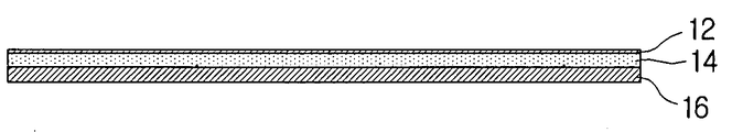
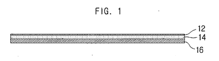
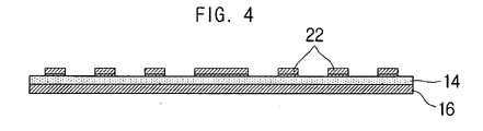
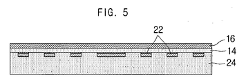
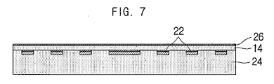
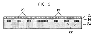
- FIG. 1 to FIG. 10 are illustrated a first seed layer 12 , an insulation layer 14 , a carrier 16 , plating resist 18 , conductive material 20 , a first circuit pattern 22 , an insulation board 24 , a second seed layer 26 , and a second circuit pattern 30 .
- a first circuit pattern 22 may be buried in one side of an insulation board 24 with a portion of the first circuit pattern 22 exposed, an insulation layer 14 may be formed thereon, and a second circuit pattern 30 may be formed on the insulation layer 14 , whereby a method is provided of readily manufacturing a circuit board of a multi-layer structure.
- the insulation layer 14 may serve as a second insulation board.
- the first circuit pattern 22 may be formed on one side of the insulation layer 14 of a carrier 16 formed by stacking an insulation layer 14 and a first seed layer 12 in order, the carrier 16 and the insulation board 24 may be stacked and pressed such that the side of the carrier 16 on which the first circuit pattern 22 is formed faces the insulation board 24 , and then the carrier 16 may be removed from the insulation board, to transfer the first circuit pattern 22 and the insulation layer 14 formed on the carrier 16 onto the insulation board 24 .
- the first circuit pattern 22 may be buried in the insulation board 24 , and the second circuit pattern 30 may be formed on the other side of the insulation layer 14 transferred to the insulation board 24 , so that a circuit board of a multi-layered structure may be manufactured that has circuit patterns of a high density.
- the insulation layer 14 may be such that is stacked temporarily on the side of the carrier 16 , and by forming the first circuit pattern 22 on the temporarily stacked insulation layer 14 , stacking the carrier 16 on the insulation board 24 such that the side of the carrier 16 faces the insulation board 24 to press the first circuit pattern 22 into the insulation board 24 , and then removing the carrier 16 , a multi-layer structure circuit board may readily be formed.
- the insulation layer 14 may be formed on the carrier 16 with a thickness of 20 to 25 ⁇ m, so that there is no electrical short-circuiting between the first circuit pattern 22 and second circuit pattern 30 .
- an insulation film made of an insulating material may be attached to the carrier 16 .
- a process of forming the first circuit pattern 22 on the insulation layer 14 of the carrier 16 , on which the insulation layer 14 and the first seed layer 12 are stacked in order, may be as follows.
- Plating resist 18 may be selectively formed on the first seed layer 12 to form an intaglio pattern corresponding to the first circuit pattern 22 , and electroplating may be performed to fill a conductive material in the intaglio pattern. Then, the plating resist 18 and the non-activated first seed layer 12 may be removed, to form the first circuit pattern 22 on the insulation layer 14 .
- a method of selectively forming plating resist 18 on the insulation layer 14 of the carrier 16 to form an intaglio pattern corresponding to the first circuit pattern 22 may include, first, coating a photosensitive material on the first seed layer 12 formed on the insulation layer 14 of the carrier 16 , fabricating a photomask in correspondence with the first circuit pattern 22 , and afterwards stacking the photomask on the side of carrier 16 coated with photosensitive material, and then exposing to ultraviolet rays. After the exposure, when the non-cured portions of the photosensitive material are developed with developing liquid, an intaglio pattern that is in correspondence with the first circuit pattern 22 may be formed on the first seed layer 12 of the carrier 16 . The cured photosensitive material that is not removed by the developing liquid may become the plating resist 18 .
- electroplating may be performed using the first seed layer 12 as the electrode, to fill the intaglio pattern with a conductive material.
- the conductive material 20 may not be formed on regions of the first seed layer 12 where the plating resist 18 is formed, due to the plating resist 18 that impedes plating.
- a conductive material known to those skilled in the art may be used, such as aluminum (Al), silver (Ag), copper (Cu), and chromium (Cr), etc., for the conductive material 20 filled in the intaglio pattern.
- filling conductive material in the intaglio pattern may include any method apparent to those skilled in the art, such as forming a seed layer on the intaglio pattern by electroless plating and using the seed layer as an electrode for electroplating, in those cases where a carrier 16 is used that does not have a first seed layer 12 , filling with conductive paste using a blade, filling with conductive ink by inkjet printing, and filling by polymerizing a conductive polymer, etc.
- the plating resist 18 may be removed, and the non-activated seed layer may be removed again, to form the first circuit pattern 22 on the insulation layer 14 of the carrier 16 .
- the non-activated seed layer refers to the regions of the seed layer which does not function as an electrode because of the plating resist 18 so that the conductive material 20 is not formed thereon.
- the carrier 16 and the insulation board 24 may be stacked, such that the side of the carrier 16 on which the first circuit pattern 22 is formed faces the insulation board 24 , and pressed together, so that the first circuit pattern 22 may be buried in the insulation board 24 .
- the insulation board 24 may include at least one of thermoplastic resin and glass epoxy resin, and when the first circuit pattern 22 is being transcribed into the insulation board 24 , the insulation board 24 may be in a softened state. That is, after softening the insulation board 24 by raising the temperature to the softening temperature of the thermoplastic and/or glass epoxy resin, burying in insulation board 24 the first circuit pattern 22 that is formed in relievo on the carrier 16 , and then separating or removing the carrier 16 , the insulation board 24 may be manufactured, when the insulation board 24 is cured, that has the first circuit pattern 22 in a buried form.
- thermosetting resin is impregnated in glass fibers to provide a semi-cured state.
- the first circuit pattern 22 may be buried in the insulation board 24 , while the insulation layer 14 may be transferred onto the insulation board 24 .
- the removal may involve etching the metal plate, or if the carrier 16 is made of a film such as of resin, etc., and is attached to the insulation layer 14 by a thermoplastic adhesive, it is possible to separate the carrier 16 by applying a particular temperature such that decreases the adhesion of the adhesive.
- a copper (Cu) plate is used as the carrier 16 , and the carrier 16 made of copper (Cu) may be removed by etching.
- a second circuit pattern 30 may be formed on the insulation layer 14 transferred onto the insulation board 24 .
- the insulation layer 14 may serve as a second insulation board, and as described above, may be formed with a thickness of 20 ⁇ m to 25 ⁇ m, so that there is no electrical short-circuiting between the first circuit pattern 22 and second circuit pattern 30 .
- a method of forming the second circuit pattern 30 on the insulation layer 14 transferred onto the insulation board 24 may include forming a second seed layer 26 on the insulation layer 14 , selectively forming plating resist 18 on the second seed layer 26 to form an intaglio pattern corresponding to the second circuit pattern 30 , and then performing electroplating using the second seed layer 26 as the electrode to fill conductive material in the intaglio pattern. Next, by removing the plating resist 18 and the non-activated second seed layer 26 , the second circuit pattern 30 may be formed on the insulation layer 14 . The same method may be used for forming the second circuit pattern 30 on the insulation layer 14 , as the method described above for forming the first circuit pattern 22 on the insulation layer 14 of the carrier 16 , and thus the description will not be repeated.
- a simple method may be used to manufacture a board in which the insulation board 24 is stacked in two layers. (In this embodiment, the insulation board 24 and the insulation layer 14 form a two-layer structure.)
- FIG. 11 , FIG. 12 , FIG. 13 , FIG. 14 , FIG. 15 , FIG. 16 , FIG. 17 , FIG. 18 and FIG. 19 represent a flow diagram illustrating a method of manufacturing a circuit board according to another embodiment of the invention.
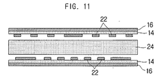
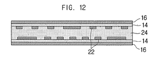
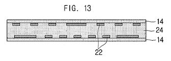
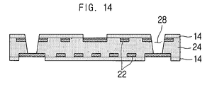
- insulation layers 14 In FIG. 11 to FIG. 19 are illustrated insulation layers 14 , carriers 16 , plating resist 18 , conductive material 20 , first circuit patterns 22 , an insulation board 24 , second seed layers 26 , via holes 28 , second circuit patterns 30 , and solder resist 32 .
- two carriers 16 are used to form two layers of circuit patterns each on both sides of the insulation board 24 , thereby providing a method of manufacturing a board having a four-layer structure.
- a first circuit pattern 22 may be formed on each insulation layer 14 of the two carriers 16 , on which insulation layers 14 and seed layers are stacked in order.
- the two carriers 16 are stacked such that the sides on which the first circuit patterns 22 are formed face either side of the insulation board 24 and then pressed together, so that the first circuit pattern 22 is buried each in both sides of the insulation board 24 .
- the first circuit pattern 22 may be buried each in both sides of the insulation board 24 , while the insulation layer 14 may be transferred each onto both sides of the insulation board 24 .
- a board may be manufactured that has insulation boards 24 stacked in three layers. (In this embodiment, the insulation board 24 and the two insulation layers 14 form a three-layer structure.)
- via holes 28 may be processed to electrically interconnect the first circuit patterns 22 and second circuit patterns 30 formed on the two insulation layers 14 and the insulation board 24 .
- the second circuit pattern 30 may be formed on each of the two insulation layers 14 , where a method of forming the second circuit patterns 30 may include first forming second seed layers 26 by electroless plating to include the inner walls of the via holes 28 , selectively forming plating resist 18 on the second seed layers 26 to form intaglio patterns corresponding to the second circuit patterns 30 , and then filling conductive material 20 in the intaglio patterns by electroplating.
- a method of forming the second circuit patterns 30 may include first forming second seed layers 26 by electroless plating to include the inner walls of the via holes 28 , selectively forming plating resist 18 on the second seed layers 26 to form intaglio patterns corresponding to the second circuit patterns 30 , and then filling conductive material 20 in the intaglio patterns by electroplating.
- the plating resist 18 and non-activated second seed layers may be removed.
- solder resist 32 may be applied to protect the surface of the board as well as the circuits exposed at the outer layers.
- a gold plating process may be performed at the pad portions where a semiconductor chip, etc., is to be coupled.
- FIG. 20 is a flowchart illustrating a method of manufacturing a circuit board according to an embodiment of the invention.
- a first circuit pattern may be formed on the insulation layer of a carrier formed by stacking in order an insulation layer and a first seed layer.
- the insulation layer stacked on the carrier may be formed with a thickness of 20 to 25 ⁇ m, so that there is no electrical short-circuiting between the first circuit pattern and second circuit pattern.
- the insulation layer may be formed on the carrier by attaching an insulation film made of an insulating material onto the carrier.
- a process of forming the first circuit pattern on the insulation layer of the carrier, on which the insulation layer and the first seed layer are stacked in order may include selectively forming plating resist on the first seed layer to form an intaglio pattern corresponding to the first circuit pattern, performing electroplating to fill a conductive material in the intaglio pattern, and then removing the plating resist and the non-activated first seed layer, to form the first circuit pattern on the insulation layer.
- a method of selectively forming plating resist on the insulation layer of the carrier to form an intaglio pattern corresponding to the first circuit pattern may include, first, coating a photosensitive material on the first seed layer formed on the insulation layer of the carrier, fabricating a photomask in correspondence with the first circuit pattern, and afterwards stacking the photomask on the side of carrier coated with photosensitive material, and then exposing to ultraviolet rays. After the exposure, when the non-cured portions of the photosensitive material are developed with developing liquid, an intaglio pattern that is in correspondence with the first circuit pattern may be formed on the first seed layer of the carrier. The cured photosensitive material that is not removed by the developing liquid may become the plating resist (S 110 ).
- electroplating may be performed using the first seed layer as the electrode, to fill the intaglio pattern with a conductive material.
- the conductive material may not be formed on regions of the first seed layer where the plating resist is formed, due to the plating resist that impedes the plating.
- a conductive material apparent to those skilled in the art may be used for the conductive material filled in the intaglio pattern, such as aluminum (Al), silver (Ag), copper (Cu), and chromium (Cr), etc. (S 120 )
- the plating resist may be removed (S 130 ), and the non-activated seed layer may be removed again, to form the first circuit pattern on the insulation layer of the carrier.
- the non-activated seed layer refers to the regions of the seed layer which does not function as an electrode because of the plating resist so that the conductive material is not formed thereon (S 140 ).
- the carrier and the insulation board may be stacked such that the side of the carrier on which the first circuit pattern is formed faces the insulation board, and may be pressed together, so that the first circuit pattern may be buried in the insulation board.
- the carrier may be separated or removed, after the carrier and the insulation board are pressed such that the first circuit pattern is buried in the insulation board, whereby the first circuit pattern may be buried in the insulation board, while the insulation layer may be transferred onto the insulation board.
- the removal may involve etching the metal plate, or if the carrier is made of a film such as of resin, etc., and is attached to the insulation layer by a thermoplastic adhesive, it is possible to separate the carrier by applying a particular temperature such that decreases the adhesion of the adhesive.
- a copper (Cu) plate may be used as the carrier, and the carrier made of copper (Cu) may be removed by etching.
- a second circuit pattern may be formed on the insulation layer transferred onto the insulation board.
- the insulation layer may serve as a second insulation board, and as described above, may be formed with a thickness of 20 to 25 ⁇ m, so that there is no electrical short-circuiting between the first circuit pattern and second circuit pattern.
- a method of forming the second circuit pattern on the insulation layer transferred onto the insulation board may include forming a second seed layer on the insulation layer (S 410 ), selectively forming plating resist on the second seed layer to form an intaglio pattern corresponding to the second circuit pattern (S 420 ), and then performing electroplating using the second seed layer as the electrode to fill conductive material in the intaglio pattern (S 430 ). Next, by removing the plating resist and the non-activated second seed layer, the second circuit pattern may be formed on the insulation layer (S 440 , S 450 ). The same method may be used for forming the second circuit pattern on the insulation layer, as the method described above for forming the first circuit pattern on the insulation layer of the carrier, and thus the description will not be repeated.
- certain aspects of the invention allow fine pitch circuit patterns, to enable the manufacture of fine circuit patterns of high density on the board, and allow the manufacture of a multi-layer circuit board with a simple process.
- a circuit board of a multi-layered structure can be manufactured by burying the circuit patterns in the board and transcribing thin insulation layers onto the board, to reduce the overall thickness of the board.
- circuits can be formed inside the board, there can be less peeling, as well as greater evenness and easier heat release. In addition, there is less likelihood of bending of the circuit board, and higher reliability with respect to ion migration between adjacent circuits.
Landscapes
- Engineering & Computer Science (AREA)
- Manufacturing & Machinery (AREA)
- Microelectronics & Electronic Packaging (AREA)
- Manufacturing Of Printed Wiring (AREA)
- Production Of Multi-Layered Print Wiring Board (AREA)
Abstract
Description
- This application claims the benefit of Korean Patent Application No. 10-2006-0105924 filed with the Korean Intellectual Property Office on Oct. 30, 2006, the disclosure of which is incorporated herein by reference in its entirety.
- 1. Technical Field
- The present invention relates to a method of manufacturing a circuit board.
- 2. Description of the Related Art
- With advances in the electronics industry, there is a growing demand for electronic components, such as in mobile devices, that provide higher performance, more functionality, and smaller sizes. Thus, there is active ongoing research for methods of manufacturing high-density boards for surface-mounted components, such as in an SiP (system in package) or 3D package, etc.
- A manufacture of a conventional multi-layer circuit board in producing a board for high-density mounted components may be completed by processing holes in a double-sided copper clad laminate using a drill, performing plating inside the holes, etching the copper foil on both sides to form circuit patterns, thermal pressing several double-sided printed circuit boards having circuit patterns formed thereon with the insulating adhesive of prepreg interposed in-between, forming holes in predetermined positions of the stacked multi-layer circuit board using a drill, completing interlayer connection by plating the multi-layer circuit board to form plating layers inside the holes, and finally etching the outermost layers to form the desired circuit patterns.
- Such a manufacturing process for a conventional multi-layer circuit board may entail a complicated process, and may make it difficult to form fine circuit patterns.
- Also, as the overall thickness of the multi-layer circuit board is great, it is difficult to implement thin boards, and as undercutting may occur at the attachment portions between the circuit and the board, the circuits are liable to be peeled off from the board.
- An aspect of the invention is to provide a method of manufacturing a circuit board, which allows fine pitch circuit patterns to enable the manufacture of fine circuit patterns of high density on the board, and which allows the manufacture of a multi-layer circuit board with a simple process.
- Also, another aspect of the invention is to provide a method of manufacturing a circuit board, with which a circuit board of a multi-layered structure may be manufactured by burying the circuit patterns in the board and transcribing thin insulation layers onto the board, to reduce the overall thickness of the board.
- One aspect of the invention provides a method of manufacturing a circuit board that includes: forming a first circuit pattern on the insulation layer of a carrier, in which an insulation layer and a first seed layer are stacked in order; stacking and pressing the carrier and an insulation board with the side of the carrier having the first circuit pattern facing the insulation board; removing the carrier to transfer the first circuit pattern and the insulation layer onto the insulation board; and forming a second circuit pattern on the insulation layer transferred to the insulation board.
- In forming the first circuit pattern, the insulation layer may be formed with a thickness of 20 μm to 25 μm in the carrier.
- Also, in forming the first circuit pattern, the insulation layer may be formed by attaching an insulation film on the carrier.
- Forming the first circuit pattern may include: selectively forming plating resist on the first seed layer to form an intaglio pattern corresponding to the first circuit pattern; filling conductive material in the intaglio pattern by performing electroplating; removing the plating resist; and removing the non-activated first seed layer.
- The carrier may be a metal plate, in which case the removing may be performed by etching the metal plate.
- Forming the second circuit pattern may include: forming a second seed layer on the insulation layer; selectively forming plating resist on the second seed layer to form an intaglio pattern corresponding to the second circuit pattern; filling conductive material in the intaglio pattern by performing electroplating; removing the plating resist; and removing the non-activated second seed layer.
- In certain embodiments, forming the first circuit pattern may include forming a first circuit pattern on the insulation layer of each of two carriers, the stacking and pressing may include stacking and pressing the two carriers and an insulation board such that the sides of the carriers having the first circuit patterns formed thereon face either side of the insulation board, the removing may include removing the two carriers, and forming the second circuit pattern may include forming a second circuit pattern on the other side of each of the insulation layers.
- In some examples, the method may further include forming at least one via hole in the insulation board, before forming the second circuit pattern on the other side of each of the insulation layers, and may further include selectively coating solder resist on the insulation board, after forming the second circuit pattern on the other side of each of the insulation layers.
- Additional aspects and advantages of the present invention will be set forth in part in the description which follows, and in part will be obvious from the description, or may be learned by practice of the invention.
-
FIG. 1 ,FIG. 2 ,FIG. 3 ,FIG. 4 ,FIG. 5 ,FIG. 6 ,FIG. 7 ,FIG. 8 ,FIG. 9 andFIG. 10 represent a flow diagram illustrating a method of manufacturing a circuit board according to an embodiment of the invention. -
FIG. 11 ,FIG. 12 ,FIG. 13 ,FIG. 14 ,FIG. 15 ,FIG. 16 ,FIG. 17 ,FIG. 18 andFIG. 19 represent a flow diagram illustrating a method of manufacturing a circuit board according to another embodiment of the invention. -
FIG. 20 is a flowchart illustrating a method of manufacturing a circuit board according to an embodiment of the invention. - The method of manufacturing a circuit board according to certain embodiments of the invention will be described below in more detail with reference to the accompanying drawings, in which those components are rendered the same reference numeral that are the same or are in correspondence, regardless of the figure number, and redundant explanations are omitted.
-
FIG. 1 ,FIG. 2 ,FIG. 3 ,FIG. 4 ,FIG. 5 ,FIG. 6 ,FIG. 7 ,FIG. 8 ,FIG. 9 andFIG. 10 represent a flow diagram illustrating a method of manufacturing a circuit board according to an embodiment of the invention. InFIG. 1 toFIG. 10 are illustrated afirst seed layer 12, aninsulation layer 14, acarrier 16, platingresist 18,conductive material 20, afirst circuit pattern 22, aninsulation board 24, asecond seed layer 26, and asecond circuit pattern 30. - In this embodiment, a
first circuit pattern 22 may be buried in one side of aninsulation board 24 with a portion of thefirst circuit pattern 22 exposed, aninsulation layer 14 may be formed thereon, and asecond circuit pattern 30 may be formed on theinsulation layer 14, whereby a method is provided of readily manufacturing a circuit board of a multi-layer structure. Here, theinsulation layer 14 may serve as a second insulation board. - More specifically, the
first circuit pattern 22 may be formed on one side of theinsulation layer 14 of acarrier 16 formed by stacking aninsulation layer 14 and afirst seed layer 12 in order, thecarrier 16 and theinsulation board 24 may be stacked and pressed such that the side of thecarrier 16 on which thefirst circuit pattern 22 is formed faces theinsulation board 24, and then thecarrier 16 may be removed from the insulation board, to transfer thefirst circuit pattern 22 and theinsulation layer 14 formed on thecarrier 16 onto theinsulation board 24. By forming thesecond circuit pattern 30 on the other side of theinsulation layer 14 transferred onto theinsulation board 24, thefirst circuit pattern 22 may be buried in theinsulation board 24, and thesecond circuit pattern 30 may be formed on the other side of theinsulation layer 14 transferred to theinsulation board 24, so that a circuit board of a multi-layered structure may be manufactured that has circuit patterns of a high density. Here, theinsulation layer 14 may be such that is stacked temporarily on the side of thecarrier 16, and by forming thefirst circuit pattern 22 on the temporarily stackedinsulation layer 14, stacking thecarrier 16 on theinsulation board 24 such that the side of thecarrier 16 faces theinsulation board 24 to press thefirst circuit pattern 22 into theinsulation board 24, and then removing thecarrier 16, a multi-layer structure circuit board may readily be formed. Here, theinsulation layer 14 may be formed on thecarrier 16 with a thickness of 20 to 25 μm, so that there is no electrical short-circuiting between thefirst circuit pattern 22 andsecond circuit pattern 30. To form theinsulation layer 14 on thecarrier 16, an insulation film made of an insulating material may be attached to thecarrier 16. - A process of forming the
first circuit pattern 22 on theinsulation layer 14 of thecarrier 16, on which theinsulation layer 14 and thefirst seed layer 12 are stacked in order, may be as follows.Plating resist 18 may be selectively formed on thefirst seed layer 12 to form an intaglio pattern corresponding to thefirst circuit pattern 22, and electroplating may be performed to fill a conductive material in the intaglio pattern. Then, the plating resist 18 and the non-activatedfirst seed layer 12 may be removed, to form thefirst circuit pattern 22 on theinsulation layer 14. - A method of selectively forming plating resist 18 on the
insulation layer 14 of thecarrier 16 to form an intaglio pattern corresponding to thefirst circuit pattern 22 may include, first, coating a photosensitive material on thefirst seed layer 12 formed on theinsulation layer 14 of thecarrier 16, fabricating a photomask in correspondence with thefirst circuit pattern 22, and afterwards stacking the photomask on the side ofcarrier 16 coated with photosensitive material, and then exposing to ultraviolet rays. After the exposure, when the non-cured portions of the photosensitive material are developed with developing liquid, an intaglio pattern that is in correspondence with thefirst circuit pattern 22 may be formed on thefirst seed layer 12 of thecarrier 16. The cured photosensitive material that is not removed by the developing liquid may become the platingresist 18. - When the intaglio pattern that is in correspondence with the
first circuit pattern 22 is formed on thefirst seed layer 12 of thecarrier 16, electroplating may be performed using thefirst seed layer 12 as the electrode, to fill the intaglio pattern with a conductive material. Theconductive material 20 may not be formed on regions of thefirst seed layer 12 where the plating resist 18 is formed, due to the plating resist 18 that impedes plating. A conductive material known to those skilled in the art may be used, such as aluminum (Al), silver (Ag), copper (Cu), and chromium (Cr), etc., for theconductive material 20 filled in the intaglio pattern. - Besides the present embodiment, filling conductive material in the intaglio pattern may include any method apparent to those skilled in the art, such as forming a seed layer on the intaglio pattern by electroless plating and using the seed layer as an electrode for electroplating, in those cases where a
carrier 16 is used that does not have afirst seed layer 12, filling with conductive paste using a blade, filling with conductive ink by inkjet printing, and filling by polymerizing a conductive polymer, etc. - When the intaglio pattern corresponding to the
first circuit pattern 22 is filled with conductive material by electroplating, theplating resist 18 may be removed, and the non-activated seed layer may be removed again, to form thefirst circuit pattern 22 on theinsulation layer 14 of thecarrier 16. - Here, the non-activated seed layer refers to the regions of the seed layer which does not function as an electrode because of the plating resist 18 so that the
conductive material 20 is not formed thereon. - When the
first circuit pattern 22 is formed on theinsulation layer 14 of thecarrier 16, thecarrier 16 and theinsulation board 24 may be stacked, such that the side of thecarrier 16 on which thefirst circuit pattern 22 is formed faces theinsulation board 24, and pressed together, so that thefirst circuit pattern 22 may be buried in theinsulation board 24. - The
insulation board 24 may include at least one of thermoplastic resin and glass epoxy resin, and when thefirst circuit pattern 22 is being transcribed into theinsulation board 24, theinsulation board 24 may be in a softened state. That is, after softening theinsulation board 24 by raising the temperature to the softening temperature of the thermoplastic and/or glass epoxy resin, burying ininsulation board 24 thefirst circuit pattern 22 that is formed in relievo on thecarrier 16, and then separating or removing thecarrier 16, theinsulation board 24 may be manufactured, when theinsulation board 24 is cured, that has thefirst circuit pattern 22 in a buried form. - Here, it is also possible to use prepreg for the
insulation board 24, in which thermosetting resin is impregnated in glass fibers to provide a semi-cured state. - When the
carrier 16 is separated or removed after thecarrier 16 and theinsulation board 24 are pressed such that thefirst circuit pattern 22 is buried in theinsulation board 24, thefirst circuit pattern 22 may be buried in theinsulation board 24, while theinsulation layer 14 may be transferred onto theinsulation board 24. - With regards methods of removing the
carrier 16, if thecarrier 16 is made of a metal plate, the removal may involve etching the metal plate, or if thecarrier 16 is made of a film such as of resin, etc., and is attached to theinsulation layer 14 by a thermoplastic adhesive, it is possible to separate thecarrier 16 by applying a particular temperature such that decreases the adhesion of the adhesive. In this embodiment, a copper (Cu) plate is used as thecarrier 16, and thecarrier 16 made of copper (Cu) may be removed by etching. - After removing the
carrier 16, asecond circuit pattern 30 may be formed on theinsulation layer 14 transferred onto theinsulation board 24. In this case, theinsulation layer 14 may serve as a second insulation board, and as described above, may be formed with a thickness of 20 μm to 25 μm, so that there is no electrical short-circuiting between thefirst circuit pattern 22 andsecond circuit pattern 30. - A method of forming the
second circuit pattern 30 on theinsulation layer 14 transferred onto theinsulation board 24 may include forming asecond seed layer 26 on theinsulation layer 14, selectively forming plating resist 18 on thesecond seed layer 26 to form an intaglio pattern corresponding to thesecond circuit pattern 30, and then performing electroplating using thesecond seed layer 26 as the electrode to fill conductive material in the intaglio pattern. Next, by removing the plating resist 18 and the non-activatedsecond seed layer 26, thesecond circuit pattern 30 may be formed on theinsulation layer 14. The same method may be used for forming thesecond circuit pattern 30 on theinsulation layer 14, as the method described above for forming thefirst circuit pattern 22 on theinsulation layer 14 of thecarrier 16, and thus the description will not be repeated. - As described above, a simple method may be used to manufacture a board in which the
insulation board 24 is stacked in two layers. (In this embodiment, theinsulation board 24 and theinsulation layer 14 form a two-layer structure.) -
FIG. 11 ,FIG. 12 ,FIG. 13 ,FIG. 14 ,FIG. 15 ,FIG. 16 ,FIG. 17 ,FIG. 18 andFIG. 19 represent a flow diagram illustrating a method of manufacturing a circuit board according to another embodiment of the invention. InFIG. 11 toFIG. 19 are illustrated insulation layers 14,carriers 16, plating resist 18,conductive material 20,first circuit patterns 22, aninsulation board 24, second seed layers 26, viaholes 28,second circuit patterns 30, and solder resist 32. - In this embodiment, two
carriers 16 are used to form two layers of circuit patterns each on both sides of theinsulation board 24, thereby providing a method of manufacturing a board having a four-layer structure. - According to the method described above, a
first circuit pattern 22 may be formed on eachinsulation layer 14 of the twocarriers 16, on which insulation layers 14 and seed layers are stacked in order. - When the
first circuit pattern 22 is formed on each of the insulation layers 14 of the twocarriers 16, the twocarriers 16 are stacked such that the sides on which thefirst circuit patterns 22 are formed face either side of theinsulation board 24 and then pressed together, so that thefirst circuit pattern 22 is buried each in both sides of theinsulation board 24. - When the two
carriers 16 are separated or removed after the twocarriers 16 are pressed with theinsulation board 24 interposed in-between, such that thefirst circuit pattern 22 is buried in either side of theinsulation board 24, thefirst circuit pattern 22 may be buried each in both sides of theinsulation board 24, while theinsulation layer 14 may be transferred each onto both sides of theinsulation board 24. In other words, a board may be manufactured that hasinsulation boards 24 stacked in three layers. (In this embodiment, theinsulation board 24 and the twoinsulation layers 14 form a three-layer structure.) - Afterwards, via
holes 28 may be processed to electrically interconnect thefirst circuit patterns 22 andsecond circuit patterns 30 formed on the twoinsulation layers 14 and theinsulation board 24. Here, it is also possible to form viaholes 28 for electrical interconnection between the circuit patterns of theinsulation board 24 and aninsulation layer 14 formed on a side of theinsulation board 24, as illustrated inFIG. 11 toFIG. 19 . - After processing the via holes 28, the
second circuit pattern 30 may be formed on each of the twoinsulation layers 14, where a method of forming thesecond circuit patterns 30 may include first forming second seed layers 26 by electroless plating to include the inner walls of the via holes 28, selectively forming plating resist 18 on the second seed layers 26 to form intaglio patterns corresponding to thesecond circuit patterns 30, and then fillingconductive material 20 in the intaglio patterns by electroplating. When the intaglio patterns are filled withconductive material 20, the plating resist 18 and non-activated second seed layers may be removed. - Afterwards, solder resist 32 may be applied to protect the surface of the board as well as the circuits exposed at the outer layers. A gold plating process may be performed at the pad portions where a semiconductor chip, etc., is to be coupled.
-
FIG. 20 is a flowchart illustrating a method of manufacturing a circuit board according to an embodiment of the invention. Referring toFIG. 20 , in operation S100, a first circuit pattern may be formed on the insulation layer of a carrier formed by stacking in order an insulation layer and a first seed layer. The insulation layer stacked on the carrier may be formed with a thickness of 20 to 25 μm, so that there is no electrical short-circuiting between the first circuit pattern and second circuit pattern. Here, the insulation layer may be formed on the carrier by attaching an insulation film made of an insulating material onto the carrier. - A process of forming the first circuit pattern on the insulation layer of the carrier, on which the insulation layer and the first seed layer are stacked in order, may include selectively forming plating resist on the first seed layer to form an intaglio pattern corresponding to the first circuit pattern, performing electroplating to fill a conductive material in the intaglio pattern, and then removing the plating resist and the non-activated first seed layer, to form the first circuit pattern on the insulation layer.
- A method of selectively forming plating resist on the insulation layer of the carrier to form an intaglio pattern corresponding to the first circuit pattern may include, first, coating a photosensitive material on the first seed layer formed on the insulation layer of the carrier, fabricating a photomask in correspondence with the first circuit pattern, and afterwards stacking the photomask on the side of carrier coated with photosensitive material, and then exposing to ultraviolet rays. After the exposure, when the non-cured portions of the photosensitive material are developed with developing liquid, an intaglio pattern that is in correspondence with the first circuit pattern may be formed on the first seed layer of the carrier. The cured photosensitive material that is not removed by the developing liquid may become the plating resist (S110).
- When the intaglio pattern in correspondence with the first circuit pattern is formed on the first seed layer of the carrier, electroplating may be performed using the first seed layer as the electrode, to fill the intaglio pattern with a conductive material. Here, the conductive material may not be formed on regions of the first seed layer where the plating resist is formed, due to the plating resist that impedes the plating. A conductive material apparent to those skilled in the art may be used for the conductive material filled in the intaglio pattern, such as aluminum (Al), silver (Ag), copper (Cu), and chromium (Cr), etc. (S120)
- When the intaglio pattern corresponding to the first circuit pattern is filled with conductive material by electroplating, the plating resist may be removed (S130), and the non-activated seed layer may be removed again, to form the first circuit pattern on the insulation layer of the carrier.
- Here, the non-activated seed layer refers to the regions of the seed layer which does not function as an electrode because of the plating resist so that the conductive material is not formed thereon (S140).
- In operation S200, the carrier and the insulation board may be stacked such that the side of the carrier on which the first circuit pattern is formed faces the insulation board, and may be pressed together, so that the first circuit pattern may be buried in the insulation board.
- In operation S300, the carrier may be separated or removed, after the carrier and the insulation board are pressed such that the first circuit pattern is buried in the insulation board, whereby the first circuit pattern may be buried in the insulation board, while the insulation layer may be transferred onto the insulation board.
- With regards methods of removing the carrier, if the carrier is made of a metal plate, the removal may involve etching the metal plate, or if the carrier is made of a film such as of resin, etc., and is attached to the insulation layer by a thermoplastic adhesive, it is possible to separate the carrier by applying a particular temperature such that decreases the adhesion of the adhesive. In this embodiment, a copper (Cu) plate may be used as the carrier, and the carrier made of copper (Cu) may be removed by etching.
- In operation S400, a second circuit pattern may be formed on the insulation layer transferred onto the insulation board. In this case, the insulation layer may serve as a second insulation board, and as described above, may be formed with a thickness of 20 to 25 μm, so that there is no electrical short-circuiting between the first circuit pattern and second circuit pattern.
- A method of forming the second circuit pattern on the insulation layer transferred onto the insulation board may include forming a second seed layer on the insulation layer (S410), selectively forming plating resist on the second seed layer to form an intaglio pattern corresponding to the second circuit pattern (S420), and then performing electroplating using the second seed layer as the electrode to fill conductive material in the intaglio pattern (S430). Next, by removing the plating resist and the non-activated second seed layer, the second circuit pattern may be formed on the insulation layer (S440, S450). The same method may be used for forming the second circuit pattern on the insulation layer, as the method described above for forming the first circuit pattern on the insulation layer of the carrier, and thus the description will not be repeated.
- As set forth above, certain aspects of the invention allow fine pitch circuit patterns, to enable the manufacture of fine circuit patterns of high density on the board, and allow the manufacture of a multi-layer circuit board with a simple process.
- Also, with certain aspects of the invention, a circuit board of a multi-layered structure can be manufactured by burying the circuit patterns in the board and transcribing thin insulation layers onto the board, to reduce the overall thickness of the board.
- Moreover, as the circuits can be formed inside the board, there can be less peeling, as well as greater evenness and easier heat release. In addition, there is less likelihood of bending of the circuit board, and higher reliability with respect to ion migration between adjacent circuits.
- While the spirit of the invention has been described in detail with reference to particular embodiments, the embodiments are for illustrative purposes only and do not limit the invention. It is to be appreciated that those skilled in the art can change or modify the embodiments without departing from the scope and spirit of the invention.
Claims (8)
Applications Claiming Priority (2)
| Application Number | Priority Date | Filing Date | Title |
|---|---|---|---|
| KR10-2006-0105924 | 2006-10-30 | ||
| KR1020060105924A KR100782407B1 (en) | 2006-10-30 | 2006-10-30 | Circuit Board Manufacturing Method |
Publications (2)
| Publication Number | Publication Date |
|---|---|
| US20080098597A1 true US20080098597A1 (en) | 2008-05-01 |
| US7937833B2 US7937833B2 (en) | 2011-05-10 |
Family
ID=39139711
Family Applications (1)
| Application Number | Title | Priority Date | Filing Date |
|---|---|---|---|
| US11/976,072 Expired - Fee Related US7937833B2 (en) | 2006-10-30 | 2007-10-19 | Method of manufacturing circuit board |
Country Status (4)
| Country | Link |
|---|---|
| US (1) | US7937833B2 (en) |
| JP (1) | JP4555852B2 (en) |
| KR (1) | KR100782407B1 (en) |
| CN (1) | CN101175378B (en) |
Cited By (5)
| Publication number | Priority date | Publication date | Assignee | Title |
|---|---|---|---|---|
| US20100012364A1 (en) * | 2008-07-21 | 2010-01-21 | Samsung Electro-Mechanics Co., Ltd. | Method of manufacturing electronic component embedded circuit board |
| US20110079421A1 (en) * | 2009-10-06 | 2011-04-07 | Young Gwan Ko | Printed circuit board and method of manufacturing the same |
| US20130112463A1 (en) * | 2009-11-25 | 2013-05-09 | Lg Innotek Co., Ltd. | Printed Circuit Board and Manufacturing Method Thereof |
| US9986642B2 (en) * | 2015-07-22 | 2018-05-29 | Ibiden Co., Ltd. | Method for manufacturing printed wiring board and printed wiring board |
| US12262465B2 (en) | 2020-05-13 | 2025-03-25 | Lg Innotek Co., Ltd. | Circuit board |
Families Citing this family (16)
| Publication number | Priority date | Publication date | Assignee | Title |
|---|---|---|---|---|
| KR100887382B1 (en) * | 2007-03-28 | 2009-03-06 | 삼성전기주식회사 | Printed Circuit Board Manufacturing Method |
| TW200948238A (en) * | 2008-05-13 | 2009-11-16 | Unimicron Technology Corp | Structure and manufacturing process for circuit board |
| KR100993342B1 (en) * | 2008-09-03 | 2010-11-10 | 삼성전기주식회사 | Printed circuit board and manufacturing method thereof |
| KR101009157B1 (en) * | 2008-11-13 | 2011-01-18 | 삼성전기주식회사 | Carrier member for circuit formation and manufacturing method of printed circuit board using the same |
| KR101025520B1 (en) * | 2008-11-26 | 2011-04-04 | 삼성전기주식회사 | Multi-layer printed circuit board manufacturing method |
| KR101021069B1 (en) | 2008-12-23 | 2011-03-11 | 안복만 | Method of forming double-sided electronic circuit with aluminum heat dissipation structure |
| KR101012403B1 (en) | 2009-10-19 | 2011-02-09 | 삼성전기주식회사 | Printed circuit board and manufacturing method thereof |
| KR101158494B1 (en) * | 2009-11-25 | 2012-06-21 | 엘지이노텍 주식회사 | PCB and Fabricating Method of the same |
| KR101115461B1 (en) | 2010-05-11 | 2012-02-24 | 엘지이노텍 주식회사 | Embedded PCB and Manufacturing method of the same |
| KR101148735B1 (en) * | 2010-07-15 | 2012-05-23 | 삼성전기주식회사 | Printed circuit board and method of manufacturing the same |
| CN103984205B (en) * | 2011-10-21 | 2018-04-27 | 联胜(中国)科技有限公司 | The production method and board structure of Thinfilm pattern |
| CN102933031A (en) * | 2012-11-14 | 2013-02-13 | 东莞市五株电子科技有限公司 | Printed circuit board and its manufacturing process |
| JP2015204379A (en) * | 2014-04-14 | 2015-11-16 | イビデン株式会社 | Printed wiring board |
| CN108933089A (en) * | 2017-05-25 | 2018-12-04 | 无锡华润安盛科技有限公司 | A kind of integrated circuit package structure and its manufacturing method |
| KR102437245B1 (en) * | 2017-10-24 | 2022-08-30 | 삼성전자주식회사 | Printed circuit board and semiconductor package including the same |
| CN110062533B (en) * | 2019-04-16 | 2022-03-18 | 安庆北化大科技园有限公司 | Application of electropolymerization technology in selective printing of solder resist ink of circuit board |
Citations (3)
| Publication number | Priority date | Publication date | Assignee | Title |
|---|---|---|---|---|
| US2692190A (en) * | 1953-08-17 | 1954-10-19 | Pritikin Nathan | Method of making inlaid circuits |
| US5712080A (en) * | 1994-02-25 | 1998-01-27 | Hitachi, Ltd. | Method for manufacturing printed circuit board |
| US6815709B2 (en) * | 2001-05-23 | 2004-11-09 | International Business Machines Corporation | Structure having flush circuitry features and method of making |
Family Cites Families (9)
| Publication number | Priority date | Publication date | Assignee | Title |
|---|---|---|---|---|
| JPH0194695A (en) * | 1987-10-06 | 1989-04-13 | Meiko Denshi Kogyo Kk | Manufacture of conductive circuit board |
| JP3750140B2 (en) * | 1994-05-10 | 2006-03-01 | 日立化成工業株式会社 | Wiring board manufacturing method |
| JP2000077848A (en) * | 1998-08-31 | 2000-03-14 | Hitachi Ltd | Method for manufacturing multilayer wiring layer |
| JP4576670B2 (en) * | 2000-06-07 | 2010-11-10 | パナソニック株式会社 | Manufacturing method of ceramic substrate |
| JP2002171066A (en) * | 2000-11-30 | 2002-06-14 | Hitachi Ltd | Method for manufacturing multilayer wiring board |
| JP2004247391A (en) * | 2003-02-12 | 2004-09-02 | Toray Ind Inc | Circuit board manufacturing method |
| EP1610599A1 (en) * | 2003-03-28 | 2005-12-28 | TDK Corporation | Multilayer substrate and method for producing same |
| JP4346541B2 (en) * | 2004-11-26 | 2009-10-21 | 日東電工株式会社 | Wiring circuit board and manufacturing method thereof |
| JP2006229115A (en) | 2005-02-21 | 2006-08-31 | North:Kk | Metal component used in manufacturing wiring substrate and method for manufacturing wiring substrate using it |
-
2006
- 2006-10-30 KR KR1020060105924A patent/KR100782407B1/en not_active Expired - Fee Related
-
2007
- 2007-10-18 JP JP2007271056A patent/JP4555852B2/en not_active Expired - Fee Related
- 2007-10-19 US US11/976,072 patent/US7937833B2/en not_active Expired - Fee Related
- 2007-10-23 CN CN200710165661XA patent/CN101175378B/en not_active Expired - Fee Related
Patent Citations (3)
| Publication number | Priority date | Publication date | Assignee | Title |
|---|---|---|---|---|
| US2692190A (en) * | 1953-08-17 | 1954-10-19 | Pritikin Nathan | Method of making inlaid circuits |
| US5712080A (en) * | 1994-02-25 | 1998-01-27 | Hitachi, Ltd. | Method for manufacturing printed circuit board |
| US6815709B2 (en) * | 2001-05-23 | 2004-11-09 | International Business Machines Corporation | Structure having flush circuitry features and method of making |
Cited By (7)
| Publication number | Priority date | Publication date | Assignee | Title |
|---|---|---|---|---|
| US20100012364A1 (en) * | 2008-07-21 | 2010-01-21 | Samsung Electro-Mechanics Co., Ltd. | Method of manufacturing electronic component embedded circuit board |
| US8201324B2 (en) | 2008-07-21 | 2012-06-19 | Samsung Electro-Mechanics Co., Ltd. | Method of manufacturing electronic component embedded circuit board |
| US20110079421A1 (en) * | 2009-10-06 | 2011-04-07 | Young Gwan Ko | Printed circuit board and method of manufacturing the same |
| US20130112463A1 (en) * | 2009-11-25 | 2013-05-09 | Lg Innotek Co., Ltd. | Printed Circuit Board and Manufacturing Method Thereof |
| US9532462B2 (en) * | 2009-11-25 | 2016-12-27 | Lg Innotek Co., Ltd. | Printed circuit board and manufacturing method thereof |
| US9986642B2 (en) * | 2015-07-22 | 2018-05-29 | Ibiden Co., Ltd. | Method for manufacturing printed wiring board and printed wiring board |
| US12262465B2 (en) | 2020-05-13 | 2025-03-25 | Lg Innotek Co., Ltd. | Circuit board |
Also Published As
| Publication number | Publication date |
|---|---|
| JP4555852B2 (en) | 2010-10-06 |
| US7937833B2 (en) | 2011-05-10 |
| JP2008112993A (en) | 2008-05-15 |
| CN101175378A (en) | 2008-05-07 |
| KR100782407B1 (en) | 2007-12-05 |
| CN101175378B (en) | 2010-09-08 |
Similar Documents
| Publication | Publication Date | Title |
|---|---|---|
| US7937833B2 (en) | Method of manufacturing circuit board | |
| US8124880B2 (en) | Circuit board and method for manufacturing thereof | |
| KR100792352B1 (en) | Bottom substrate of package on package and manufacturing method thereof | |
| KR100867148B1 (en) | Printed Circuit Board and Manufacturing Method | |
| US8058558B2 (en) | Printed circuit board and manufacturing method thereof | |
| JP4538486B2 (en) | Multilayer substrate and manufacturing method thereof | |
| US7730612B2 (en) | Method of manufacturing component-embedded printed circuit board | |
| JP2007142403A (en) | Printed board and manufacturing method of same | |
| TWI479972B (en) | Multi-layer flexible printed wiring board and manufacturing method thereof | |
| WO2011135900A1 (en) | Build-up multilayer printed wiring board and production method therefor | |
| JP2007324559A (en) | Multilayer circuit board with fine pitch and fabricating method thereof | |
| KR100857165B1 (en) | Circuit Board Manufacturing Method | |
| KR100993342B1 (en) | Printed circuit board and manufacturing method thereof | |
| JP5302920B2 (en) | Manufacturing method of multilayer wiring board | |
| KR20110010427A (en) | Odd-layer printed circuit board and manufacturing method thereof | |
| KR100716809B1 (en) | Printed Circuit Board Using Anisotropic Conductive Film and Manufacturing Method Thereof | |
| US20030113951A1 (en) | Method for manufacturing multi-layer package substrates | |
| JP2011222962A (en) | Print circuit board and method of manufacturing the same | |
| KR100726238B1 (en) | Multi-layer printed circuit board manufacturing method | |
| JP4926676B2 (en) | Manufacturing method of multilayer printed wiring board | |
| KR100796981B1 (en) | Printed Circuit Board Manufacturing Method |
Legal Events
| Date | Code | Title | Description |
|---|---|---|---|
| AS | Assignment |
Owner name: SAMSUNG ELECTRO-MECHANICS CO., LTD., KOREA, REPUBL Free format text: ASSIGNMENT OF ASSIGNORS INTEREST;ASSIGNORS:JUNG, HOE-KU;YOO, JE-GWANG;KANG, MYUNG-SAM;AND OTHERS;REEL/FRAME:020042/0530 Effective date: 20070921 |
|
| STCF | Information on status: patent grant |
Free format text: PATENTED CASE |
|
| CC | Certificate of correction | ||
| FEPP | Fee payment procedure |
Free format text: PAYOR NUMBER ASSIGNED (ORIGINAL EVENT CODE: ASPN); ENTITY STATUS OF PATENT OWNER: LARGE ENTITY |
|
| FPAY | Fee payment |
Year of fee payment: 4 |
|
| FEPP | Fee payment procedure |
Free format text: MAINTENANCE FEE REMINDER MAILED (ORIGINAL EVENT CODE: REM.); ENTITY STATUS OF PATENT OWNER: LARGE ENTITY |
|
| LAPS | Lapse for failure to pay maintenance fees |
Free format text: PATENT EXPIRED FOR FAILURE TO PAY MAINTENANCE FEES (ORIGINAL EVENT CODE: EXP.); ENTITY STATUS OF PATENT OWNER: LARGE ENTITY |
|
| STCH | Information on status: patent discontinuation |
Free format text: PATENT EXPIRED DUE TO NONPAYMENT OF MAINTENANCE FEES UNDER 37 CFR 1.362 |
|
| FP | Lapsed due to failure to pay maintenance fee |
Effective date: 20190510 |