US20070279727A1 - Display apparatus with optical cavities - Google Patents
Display apparatus with optical cavities Download PDFInfo
- Publication number
- US20070279727A1 US20070279727A1 US11/528,191 US52819106A US2007279727A1 US 20070279727 A1 US20070279727 A1 US 20070279727A1 US 52819106 A US52819106 A US 52819106A US 2007279727 A1 US2007279727 A1 US 2007279727A1
- Authority
- US
- United States
- Prior art keywords
- light
- display
- light guide
- facing reflective
- reflective layer
- Prior art date
- Legal status (The legal status is an assumption and is not a legal conclusion. Google has not performed a legal analysis and makes no representation as to the accuracy of the status listed.)
- Granted
Links
- 230000003287 optical effect Effects 0.000 title claims description 47
- 229910052751 metal Inorganic materials 0.000 claims description 45
- 239000002184 metal Substances 0.000 claims description 45
- 239000000758 substrate Substances 0.000 claims description 41
- 238000000034 method Methods 0.000 claims description 28
- 239000004033 plastic Substances 0.000 claims description 19
- 239000011521 glass Substances 0.000 claims description 18
- 239000002131 composite material Substances 0.000 claims description 14
- 230000004907 flux Effects 0.000 claims description 13
- 239000000463 material Substances 0.000 claims description 13
- 230000015572 biosynthetic process Effects 0.000 claims description 5
- 238000002347 injection Methods 0.000 claims description 5
- 239000007924 injection Substances 0.000 claims description 5
- 239000010408 film Substances 0.000 description 87
- 238000000605 extraction Methods 0.000 description 57
- 230000000712 assembly Effects 0.000 description 40
- 238000000429 assembly Methods 0.000 description 40
- 238000004064 recycling Methods 0.000 description 33
- 238000009826 distribution Methods 0.000 description 31
- 230000006870 function Effects 0.000 description 16
- 239000004593 Epoxy Substances 0.000 description 15
- 238000013461 design Methods 0.000 description 15
- 238000002310 reflectometry Methods 0.000 description 15
- 238000005286 illumination Methods 0.000 description 13
- 239000010409 thin film Substances 0.000 description 13
- 239000004973 liquid crystal related substance Substances 0.000 description 12
- 239000003973 paint Substances 0.000 description 11
- 238000000576 coating method Methods 0.000 description 10
- 230000000694 effects Effects 0.000 description 9
- 239000012530 fluid Substances 0.000 description 9
- 230000008859 change Effects 0.000 description 8
- 230000002708 enhancing effect Effects 0.000 description 8
- 230000008901 benefit Effects 0.000 description 7
- 230000001965 increasing effect Effects 0.000 description 7
- 150000001875 compounds Chemical class 0.000 description 6
- 239000011248 coating agent Substances 0.000 description 5
- 230000002349 favourable effect Effects 0.000 description 5
- 239000007788 liquid Substances 0.000 description 5
- 239000007787 solid Substances 0.000 description 5
- 239000000853 adhesive Substances 0.000 description 4
- 230000001070 adhesive effect Effects 0.000 description 4
- 230000015556 catabolic process Effects 0.000 description 4
- 238000000151 deposition Methods 0.000 description 4
- 230000008021 deposition Effects 0.000 description 4
- 238000001704 evaporation Methods 0.000 description 4
- 230000008020 evaporation Effects 0.000 description 4
- 238000005259 measurement Methods 0.000 description 4
- 150000002739 metals Chemical class 0.000 description 4
- -1 methyl-siloxanes Chemical class 0.000 description 4
- 238000004544 sputter deposition Methods 0.000 description 4
- OKKJLVBELUTLKV-UHFFFAOYSA-N Methanol Chemical compound OC OKKJLVBELUTLKV-UHFFFAOYSA-N 0.000 description 3
- 229910052779 Neodymium Inorganic materials 0.000 description 3
- 229910045601 alloy Inorganic materials 0.000 description 3
- 239000000956 alloy Substances 0.000 description 3
- 229910052782 aluminium Inorganic materials 0.000 description 3
- 239000003518 caustics Substances 0.000 description 3
- 229910052804 chromium Inorganic materials 0.000 description 3
- 230000000295 complement effect Effects 0.000 description 3
- 229910052802 copper Inorganic materials 0.000 description 3
- 238000006731 degradation reaction Methods 0.000 description 3
- 238000005516 engineering process Methods 0.000 description 3
- 238000005530 etching Methods 0.000 description 3
- 229910052737 gold Inorganic materials 0.000 description 3
- 238000001746 injection moulding Methods 0.000 description 3
- 238000007733 ion plating Methods 0.000 description 3
- 238000000608 laser ablation Methods 0.000 description 3
- 238000001182 laser chemical vapour deposition Methods 0.000 description 3
- 239000002991 molded plastic Substances 0.000 description 3
- 229910052750 molybdenum Inorganic materials 0.000 description 3
- 229910052759 nickel Inorganic materials 0.000 description 3
- 229910052758 niobium Inorganic materials 0.000 description 3
- 238000000206 photolithography Methods 0.000 description 3
- 238000004382 potting Methods 0.000 description 3
- 230000005855 radiation Effects 0.000 description 3
- 229910052710 silicon Inorganic materials 0.000 description 3
- 229910052709 silver Inorganic materials 0.000 description 3
- 229910052715 tantalum Inorganic materials 0.000 description 3
- 238000012360 testing method Methods 0.000 description 3
- 229910052719 titanium Inorganic materials 0.000 description 3
- 238000007740 vapor deposition Methods 0.000 description 3
- KVNYFPKFSJIPBJ-UHFFFAOYSA-N 1,2-diethylbenzene Chemical compound CCC1=CC=CC=C1CC KVNYFPKFSJIPBJ-UHFFFAOYSA-N 0.000 description 2
- LFQSCWFLJHTTHZ-UHFFFAOYSA-N Ethanol Chemical compound CCO LFQSCWFLJHTTHZ-UHFFFAOYSA-N 0.000 description 2
- 239000004965 Silica aerogel Substances 0.000 description 2
- VYPSYNLAJGMNEJ-UHFFFAOYSA-N Silicium dioxide Chemical compound O=[Si]=O VYPSYNLAJGMNEJ-UHFFFAOYSA-N 0.000 description 2
- 238000004458 analytical method Methods 0.000 description 2
- 238000013459 approach Methods 0.000 description 2
- 210000002858 crystal cell Anatomy 0.000 description 2
- 239000004811 fluoropolymer Substances 0.000 description 2
- 229920002313 fluoropolymer Polymers 0.000 description 2
- 230000006872 improvement Effects 0.000 description 2
- 238000010348 incorporation Methods 0.000 description 2
- 238000003780 insertion Methods 0.000 description 2
- 239000011159 matrix material Substances 0.000 description 2
- 230000007246 mechanism Effects 0.000 description 2
- 239000002985 plastic film Substances 0.000 description 2
- 229920006255 plastic film Polymers 0.000 description 2
- 239000011148 porous material Substances 0.000 description 2
- 238000012545 processing Methods 0.000 description 2
- 230000002829 reductive effect Effects 0.000 description 2
- 230000004044 response Effects 0.000 description 2
- 230000002441 reversible effect Effects 0.000 description 2
- 239000004065 semiconductor Substances 0.000 description 2
- 229920002545 silicone oil Polymers 0.000 description 2
- 239000013598 vector Substances 0.000 description 2
- 229910001069 Ti alloy Inorganic materials 0.000 description 1
- 238000010521 absorption reaction Methods 0.000 description 1
- 238000007792 addition Methods 0.000 description 1
- 230000004075 alteration Effects 0.000 description 1
- 238000000149 argon plasma sintering Methods 0.000 description 1
- 230000009286 beneficial effect Effects 0.000 description 1
- 238000005229 chemical vapour deposition Methods 0.000 description 1
- 239000003086 colorant Substances 0.000 description 1
- 239000012141 concentrate Substances 0.000 description 1
- 239000000470 constituent Substances 0.000 description 1
- 238000010276 construction Methods 0.000 description 1
- 230000003247 decreasing effect Effects 0.000 description 1
- 230000000593 degrading effect Effects 0.000 description 1
- 239000008367 deionised water Substances 0.000 description 1
- 229910003460 diamond Inorganic materials 0.000 description 1
- 239000010432 diamond Substances 0.000 description 1
- 239000004205 dimethyl polysiloxane Substances 0.000 description 1
- 239000007888 film coating Substances 0.000 description 1
- 238000009501 film coating Methods 0.000 description 1
- UQEAIHBTYFGYIE-UHFFFAOYSA-N hexamethyldisiloxane Chemical compound C[Si](C)(C)O[Si](C)(C)C UQEAIHBTYFGYIE-UHFFFAOYSA-N 0.000 description 1
- 230000003116 impacting effect Effects 0.000 description 1
- 230000037431 insertion Effects 0.000 description 1
- 230000000670 limiting effect Effects 0.000 description 1
- 239000000314 lubricant Substances 0.000 description 1
- 238000004519 manufacturing process Methods 0.000 description 1
- 238000012986 modification Methods 0.000 description 1
- 230000004048 modification Effects 0.000 description 1
- 239000012788 optical film Substances 0.000 description 1
- 238000012856 packing Methods 0.000 description 1
- 230000037361 pathway Effects 0.000 description 1
- 230000000737 periodic effect Effects 0.000 description 1
- 238000005240 physical vapour deposition Methods 0.000 description 1
- 229920000435 poly(dimethylsiloxane) Polymers 0.000 description 1
- 230000008569 process Effects 0.000 description 1
- 230000000717 retained effect Effects 0.000 description 1
- 230000003746 surface roughness Effects 0.000 description 1
- 229910052721 tungsten Inorganic materials 0.000 description 1
- 230000000007 visual effect Effects 0.000 description 1
- 238000009736 wetting Methods 0.000 description 1
Images


Classifications
-
- G—PHYSICS
- G02—OPTICS
- G02B—OPTICAL ELEMENTS, SYSTEMS OR APPARATUS
- G02B6/00—Light guides; Structural details of arrangements comprising light guides and other optical elements, e.g. couplings
- G02B6/0001—Light guides; Structural details of arrangements comprising light guides and other optical elements, e.g. couplings specially adapted for lighting devices or systems
- G02B6/0011—Light guides; Structural details of arrangements comprising light guides and other optical elements, e.g. couplings specially adapted for lighting devices or systems the light guides being planar or of plate-like form
- G02B6/0033—Means for improving the coupling-out of light from the light guide
- G02B6/005—Means for improving the coupling-out of light from the light guide provided by one optical element, or plurality thereof, placed on the light output side of the light guide
- G02B6/0055—Reflecting element, sheet or layer
-
- G—PHYSICS
- G02—OPTICS
- G02B—OPTICAL ELEMENTS, SYSTEMS OR APPARATUS
- G02B6/00—Light guides; Structural details of arrangements comprising light guides and other optical elements, e.g. couplings
- G02B6/0001—Light guides; Structural details of arrangements comprising light guides and other optical elements, e.g. couplings specially adapted for lighting devices or systems
- G02B6/0011—Light guides; Structural details of arrangements comprising light guides and other optical elements, e.g. couplings specially adapted for lighting devices or systems the light guides being planar or of plate-like form
- G02B6/0033—Means for improving the coupling-out of light from the light guide
- G02B6/0035—Means for improving the coupling-out of light from the light guide provided on the surface of the light guide or in the bulk of it
- G02B6/0036—2-D arrangement of prisms, protrusions, indentations or roughened surfaces
-
- G—PHYSICS
- G02—OPTICS
- G02B—OPTICAL ELEMENTS, SYSTEMS OR APPARATUS
- G02B6/00—Light guides; Structural details of arrangements comprising light guides and other optical elements, e.g. couplings
- G02B6/0001—Light guides; Structural details of arrangements comprising light guides and other optical elements, e.g. couplings specially adapted for lighting devices or systems
- G02B6/0011—Light guides; Structural details of arrangements comprising light guides and other optical elements, e.g. couplings specially adapted for lighting devices or systems the light guides being planar or of plate-like form
- G02B6/0033—Means for improving the coupling-out of light from the light guide
- G02B6/0035—Means for improving the coupling-out of light from the light guide provided on the surface of the light guide or in the bulk of it
- G02B6/0038—Linear indentations or grooves, e.g. arc-shaped grooves or meandering grooves, extending over the full length or width of the light guide
-
- G—PHYSICS
- G02—OPTICS
- G02B—OPTICAL ELEMENTS, SYSTEMS OR APPARATUS
- G02B6/00—Light guides; Structural details of arrangements comprising light guides and other optical elements, e.g. couplings
- G02B6/0001—Light guides; Structural details of arrangements comprising light guides and other optical elements, e.g. couplings specially adapted for lighting devices or systems
- G02B6/0011—Light guides; Structural details of arrangements comprising light guides and other optical elements, e.g. couplings specially adapted for lighting devices or systems the light guides being planar or of plate-like form
- G02B6/0033—Means for improving the coupling-out of light from the light guide
- G02B6/0035—Means for improving the coupling-out of light from the light guide provided on the surface of the light guide or in the bulk of it
- G02B6/004—Scattering dots or dot-like elements, e.g. microbeads, scattering particles, nanoparticles
- G02B6/0043—Scattering dots or dot-like elements, e.g. microbeads, scattering particles, nanoparticles provided on the surface of the light guide
-
- G—PHYSICS
- G02—OPTICS
- G02B—OPTICAL ELEMENTS, SYSTEMS OR APPARATUS
- G02B6/00—Light guides; Structural details of arrangements comprising light guides and other optical elements, e.g. couplings
- G02B6/0001—Light guides; Structural details of arrangements comprising light guides and other optical elements, e.g. couplings specially adapted for lighting devices or systems
- G02B6/0011—Light guides; Structural details of arrangements comprising light guides and other optical elements, e.g. couplings specially adapted for lighting devices or systems the light guides being planar or of plate-like form
- G02B6/0033—Means for improving the coupling-out of light from the light guide
- G02B6/005—Means for improving the coupling-out of light from the light guide provided by one optical element, or plurality thereof, placed on the light output side of the light guide
- G02B6/0053—Prismatic sheet or layer; Brightness enhancement element, sheet or layer
Definitions
- Displays built from mechanical light modulators are an attractive alternative to displays based on liquid crystal technology.
- Mechanical light modulators are fast enough to display video content with good viewing angles and with a wide range of color and grey scale. Mechanical light modulators have been successful in projection display applications. Backlit displays using mechanical light modulators have not yet demonstrated sufficiently attractive combinations of brightness and low power. There is a need in the art for displays that combine the attributes of speed, brightness, and low power.
- the invention relates to a display having an improved optical cavity to provide enhanced light directivity and efficiency.
- the invention relates to a display including an array of light modulators, a light guide, and front-facing and rear-facing reflective surfaces.
- the light guide includes a plurality of geometric light redirection centers to extract light from the backlight.
- Various embodiments of such redirection centers are described in U.S. Pat. Nos. 5,005,108; 5,202,950; 5,884,872; 6,079,838; 6,174,064; 6,731,355; 6,827,456; 7,014,349; and 7,046,905, the entireties of which are herein incorporated by reference.
- the display also includes either a turning film and or a brightness enhancing film positioned behind of the rear-facing reflective surface.
- the display includes a light injection system including a lamp and a light collimator for introducing a non-random fraction of light output by the lamp into the light guide to produce collimated light within a predetermined range of angles.
- Collimated light includes any distribution of input light where a higher-than-random percentage of light is directed towards the reflective aperture layer within a pre-determined range of angles.
- Various light collimation and injection techniques suitable for use in the display are described in U.S. Pat. Nos. 5,005,108; 5,884,872; 6,079,838; and 7,014,349, the entireties of which are herein incorporated by reference.
- the light modulators are MEMS-based light modulators, for example, shutters, which selectively interfere with light that passes through corresponding apertures in the rear-facing reflective layer.
- the shutters are liquid-based shutters, which can selectively interfere with light using a mechanism referred to as electro-wetting.
- the light modulators are liquid crystal cells.
- the array of light modulators defines a display surface.
- the display plane is preferably substantially planar.
- the light guide includes a front surface and a rear surface. In one embodiment, between about 50% to about 95% of the area of the rear surface of the light guide is substantially parallel to the display surface. In one particular embodiment, at least 50% of the area of the rear surface of the light guide is substantially parallel to the display surface. In another embodiment, at least 60% of the area of the rear surface of the light guide is substantially parallel to the display surface. In still another embodiment at least 70% of the area of the rear surface of the light guide is substantially parallel to the display surface. In a further embodiment at least 80% of the area of the rear surface of the light guide is substantially parallel to the display surface. In yet another embodiment, at least 80% of the area of the rear surface of the light guide is substantially parallel to the display surface.
- the geometric light redirectors are also referred to herein as extraction centers, extraction structures, and deflectors.
- the light redirectors' function is to extract light out of the light guide and toward the viewer.
- the light redirectors are prismatic in shape.
- the light redirectors are round, curved, trapezoidal, elliptical.
- the surfaces of the light redirectors are preferably smooth.
- the light redirectors are capable of extracting light wherein a higher-than-random percentage of light is directed towards the reflective aperture layer within a pre-determined range of angles.
- the light directors have a front surface facing a lamp and a rear surface facing away from the lamp.
- the area of the footprint of the front face of a redirector onto the front-facing reflective surface may be greater than the area of a similar footprint of the rear face of the redirector.
- the areas of the footprints of the front and rear surfaces of the light redirectors are equal.
- the packing density of the light redirectors in the light guide may vary as a function of the light redirectors' distance from the lamp.
- the rear-facing reflective layer (also referred to herein as the reflective aperture layer) includes a plurality of apertures and is positioned in front of the light guide, i.e., between the light guide and an intended viewer.
- the rear-facing reflective layer is preferably positioned behind the light modulators.
- the rear-facing reflective layer is formed from the deposition of a metal on the front surface of the light guide.
- the rear-facing reflective layer may also be formed from a dielectric mirror or from a thin film stack the includes both dielectric and metal layers.
- the rear-facing reflective layer preferably reflects light specularly with a reflectivity in the range of 90 to 98%.
- the rear-facing reflective layer is preferably positioned proximate to the array of light modulators. In one embodiment the rear-facing reflective layer positioned within 0.5 mm of the array of light modulators. In another embodiment, an array of light modulators is formed on a substrate, and the distance between the rear-facing reflective layer and the array of light modulators is less than the thickness of the substrate. In another embodiment, the rear-facing reflective layer has a pitch defining the distance between apertures, and the distance between the rear-facing reflective layer and the array of light modulators is less than the pitch.
- the apertures are associated with specific light modulators in the array of light modulators.
- the association can be one to one, one to many, or many to one.
- Each aperture allows a flux of light to pass through.
- the light modulators modulate substantially the entire flux of light passing through the aperture. More particularly, a single light modulator, in one embodiment, modulates substantially the entire flux of light passing through a single associated aperture. In another embodiment, a single light modulator modulates substantially the entire flux of light passing through multiple associated apertures. In still another embodiment, multiple light modulators, together, modulate substantially all of the flux of light passing through a single aperture.
- the front-facing reflective layer in one embodiment (also referred to herein as a back-reflector or back-reflective surface) is substantially parallel to the display surface. That is, it is preferably at an angle of less than about 10 degrees to the display surface. In one embodiment, the front-facing reflective layer is parallel to the display surface. In one implementation, the front-facing reflective layer is a metal deposited on the rear surface of the light guide. The front-facing reflective layer may also be formed from a dielectric mirror or from a thin film stack the includes both dielectric and metal layers. Alternatively, the front-facing reflective layer is separated from the light guide by an air gap.
- the front-facing reflective layer in one embodiment reflects light specularly. It preferably has a reflectivity in the range of 90 to 98%.
- Such displays concentrate emitted light within a range of angles about an axis normal to the display plane (referred to as the “display normal”). For example, light can be concentrated such that a higher-than-random percentage of light reflected off of the rear-facing reflective surface towards the front-facing reflective layer at angles within a useful range of angles about the display normal is redirected towards the reflective aperture layer at angles also within the range of useful angles about the display normal.
- the range of useful angles in various embodiments ranges from about 20 degrees to about 40 degrees from the display normal. For example, in one embodiment, the useful range of angles includes angles within 20 degrees of the display normal. In another embodiment, the useful range of angles includes angles within 30 degrees of the display normal. In still a further embodiment, the useful range of angles includes angles within 40 degrees of the display normal.
- At least 50% of the light reflected off the rear-facing reflective layer at an angle within the useful range of angles exits the light guide at an angle also within the useful range of angles.
- at least 70% of the light reflected off the rear-facing reflective layer at an angle within the useful range of angles exits the light guide at an angle also within the useful range of angles.
- at least 90% of the light reflected off the rear-facing reflective layer at an angle within the useful range of angles exits the light guide at an angle also within the useful range of angles.
- the invention in another aspect, relates to a method of forming an image using an improved optical cavity.
- the method includes providing a array of light modulators, which defines a display surface, in proximity to an optical cavity.
- the optical cavity includes a rear-facing reflective aperture layer as a front surface, a rear surface, and a light guide positioned between the front surface and the rear surface.
- Light is reflected off the rear-facing reflective aperture layer. A portion of the light is reflected to within a useful range of angles about a display axis perpendicular to the display surface. This portion of light has an initial total light intensity. The reflected light is then redirected by the rear surface of the optical cavity.
- the light redirected towards the reflective aperture layer within the useful range of angles about the display normal has an intensity of at least 50% of the initial intensity.
- the intensity of the redirected light within the useful range of angles about the display axis is at least 70% of the initial total light intensity.
- the intensity of the redirected light within the useful range of angles about the display axis is at least 90% of the initial total light intensity.
- the useful range of angles about the normal is about 40 degrees about the normal.
- the useful range of angles about the normal is about 30 degrees about the normal.
- the useful range of angles is about 20 degrees about the normal.
- conical reflectance is defined as the ability of a backlight or illumination system to receive an incoming cone of light within a pre-determined range of angles (measured with respect to an incident axis) and then re-emit or reflect that light along an equivalent exit axis where the integrated intensity (or radiant power) of the exit light, measured about the exit axis over the same pre-determined range of angles, is greater than a specified fraction of the integrated incident light.
- the incoming cone of light preferably illuminates an area of the backlight at least 2 mm in diameter and the radiant power is preferably determined by integrating reflected light over a similar or larger area.
- FIG. 1A is a cross sectional view of a display apparatus.
- FIG. 1B is a cross sectional view of another display apparatus.
- FIG. 2A is a cross sectional view of a display apparatus according to an illustrative embodiment of the invention.
- FIG. 2B is a cross sectional view of a display apparatus according to an illustrative embodiment of the invention.
- FIG. 3A is a schematic optical layout for the measurement of the property of conical reflectance
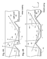
- FIG. 3B illustrates the variation in light output intensity from backlights employed in various embodiments of the invention as a function of solid angle.
- FIGS. 4A and 4B are cross sectional views of portions of a light guide along with their associated front-facing reflective layers for use in a display apparatus according to an illustrative embodiment of the invention.
- FIGS. 5A-5D are cross sectional views of portions of a light guide along with their associated front-facing reflective layers for use in a display apparatus according to an illustrative embodiment of the invention.
- FIGS. 6A-6D are cross sectional views of portions of a light guide along with their associated front-facing reflective layers for use in a display apparatus according to an illustrative embodiment of the invention.
- FIG. 7A is a cross sectional view of a display apparatus according to an illustrative embodiment of the invention.
- FIGS. 7B-7D are cross sectional views of portions of a light guide along with their associated front-facing reflective layers for use in a display apparatus according to an illustrative embodiment of the invention.
- FIGS. 8A and 8B are cross sectional views of portions of a light guide for use in a display apparatus according to an illustrative embodiment of the invention.
- FIG. 8C is an isometric view of a light guide for use in a display apparatus according to an illustrative embodiment of the invention.
- FIGS. 9A-9C are cross sectional views of portions of a light guide along with their associated front-facing reflective layers for use in a display apparatus according to an illustrative embodiment of the invention.
- FIGS. 10A , 10 B, 10 C, and 10 D are isometric views of a light guide along with associated light injection systems for use in a display according to an illustrative embodiment of the invention.
- FIGS. 11A and 11B are an isometric views of a light guide along with an associated light injection system for use in a display according to an illustrative embodiment of the invention.
- FIG. 12 is an assembly drawing of various components in a display apparatus according to an illustrative embodiment of the invention.
- FIG. 13 is an assembly drawing of various components in a display apparatus according to an illustrative embodiment of the invention.
- FIG. 14 is an assembly drawing of various components in a display apparatus according to an illustrative embodiment of the invention.
- FIG. 15 is an assembly drawing of various components in a display apparatus according to an illustrative embodiment of the invention.
- FIG. 16 is an assembly drawing of various components in a display apparatus according to an illustrative embodiment of the invention.
- FIG. 17 is a cross sectional view of a display apparatus according to an illustrative embodiment of the invention.
- FIGS. 18A and 18B are cross sectional views of portions of a light guide along with their associated front-facing reflective layers for use in a display apparatus according to an illustrative embodiment of the invention.
- FIG. 19 is a cross sectional view of a display apparatus according to an illustrative embodiment of the invention.
- FIG. 20 is a cross sectional view of a display apparatus according to an illustrative embodiment of the invention.
- FIG. 21 is a cross sectional view of a display apparatus according to an illustrative embodiment of the invention.
- U.S. patent application Ser. No. 11/218,690 entitled Methods and Apparatus for Spatial Light Modulation, describes a backlit display with increased optical efficiency which relies on an array of shutter assemblies and apertures.
- the shutter assembly in a given pixel acts to alternately either open or close the optical pathway through a corresponding aperture.
- the apertures are formed as light transmissive regions in an otherwise reflective surface, which we refer to as the reflective aperture layer.
- the display includes a second reflective surface, which can be formed as part of a backlight.
- FIG. 1A An illustration of a display apparatus as described in U.S. patent Ser. No. 11/218,690 is given in FIG. 1A .
- the apertures 102 are defined in an aperture layer 104 which can be fabricated from a reflective material.
- the apertures can be alternately opened and closed by means of shutters 106 which are formed along with electro-mechanical actuators in a shutter assembly 108 .
- the shutters are built upon a light modulation substrate 109 .
- the modulation substrate 109 is situated on top of a backlight 110 which is in turn illuminated by a lamp 112 .
- Further descriptions of mechanical actuators for opening and closing of the shutters can be found in co-owned U.S. patent Ser. No. 11/251,035, filed Oct. 14, 2005 and incorporated herein by reference.
- a display such as in FIG. 1A may have aperture openings that comprise a small fraction (5 to 25%) of the available pixel. In many cases the throughput efficiency of the light would then be limited in similar fashion, i.e. only 5 to 25% of the available illumination power in the backlight becomes available to the viewer. However, in those cases where the aperture layer 104 is formed from a reflective material, and where the backlight also possesses a back-reflective surface 114 , the backlight becomes capable of recycling rays that do not initially pass through an aperture to the viewer. An exemplary ray of such recycled light is shown as 118 in the figure. Because of these recycled light rays, a much greater fraction of the available backlight power can eventually makes its way to the viewer.
- Table 1 shows the calculated efficiency results from a series of backlights with differing fractions of aperture openings and reflective efficiencies from its metal surfaces. Throughput efficiencies as high as 75% can be achieved. Displays with such improved throughput can deliver more brightness to the viewer at equivalent lamp powers, or conversely can deliver the same brightness by means of reduced power in the backlight compared to the prior art. Displays which make use of aperture layers that have reflective or recycling properties will hereafter be referred to as reflective aperture displays.
- the display apparatus 101 includes a lamp 112 .
- lamp 112 A number of different types of lamps can be employed in these displays, including without limitation: incandescent lamps, fluorescent lamps, lasers, or light emitting diodes (LEDs).
- lamp 112 of display apparatus 101 can actually represent an assembly of multiple lamps. For instance a combination of red, green, and blue LEDs can be combined with or substituted for a white LED in a small semiconductor chip, or assembled into a small multi-lamp package.
- a lamp can represent an assembly of 4-color LEDs, for instance a combination of red, yellow, green, and blue LEDs.
- the light guide 110 includes an array of scattering centers 116 whose function is to extract light from the light guide, i.e. to deflect rays into directions that no longer satisfy the condition for total internal reflection.
- scattering centers are formed as an array of white dots.
- the scattering dots are painted with a silk screen into a random pattern to avoid artifacts to the final image. Dots formed from white paint act as diffuse reflectors which scatter reflected light into random directions, (see the result of ray 119 ), ideally with no correlation between the angle of the incoming rays and the angle of the outgoing rays.
- light that is deflected down and out of the light guide will be returned to the light guide by reflection from the reflector 114 .
- Light that is deflected up and toward the apertures, but that does not escape through an open aperture, can be returned to the light guide by reflection from the reflective surface 104 . After reflection from surface 104 the light will either reflect again from surface 114 or impinge on a dot of white paint where its direction will be randomized again.
- the density of the scattering centers 116 is adjusted to ensure the uniformity of light which is emitted from the light guide, with typically a lower density of extraction centers placed near to the lamp and a higher density placed at the furthest distances from the lamp.
- the device For portable devices, it is often or commonly the case that the device is designed for a single user, and the most common view angle will be on or about the normal to the aperture plane.
- the random or Lambertian distribution of light exiting from the apertures will be sub-optimal. Light that is emitted into the off-angles, not directly toward the viewer, can be considered as wasted light. In fact, for a Lambertian distribution only 12% of the emitted radiant power will be directed into the most forward-looking 20 degrees of solid angle. Any design which can direct a greater fraction (for instance 30% or more) of the total radiated power into a direction favorable for the user makes possible a considerable improvement in power efficiency—an important feature for portable electronics.
- a display including a reflective aperture layer can be improved, particularly for mobile use, by providing a means for concentrating light into angles closer to the display normal.
- FIG. 1B shows a display structure including a brightness enhancing film.
- the display apparatus 150 of FIG. 1B includes a light modulation substrate 159 , which in turns includes a reflective aperture layer 154 , an array of apertures 152 , shutters 156 , and shutter assemblies 158 .
- the Display apparatus 150 also includes a backlight 160 which includes a lamp 162 , scattering centers 166 , and a back-reflecting film 164 Placed between the substrates 159 and 160 are a prismatic brightness enhancing film (or BEF film) 170 and a diffusing film 172 .
- a backlight 160 which includes a lamp 162 , scattering centers 166 , and a back-reflecting film 164 Placed between the substrates 159 and 160 are a prismatic brightness enhancing film (or BEF film) 170 and a diffusing film 172 .
- Prismatic brightness enhancing films are known to increase the luminance in the forward direction (along the display normal) in liquid crystal displays by amounts of 50% to 100%.
- the BEF films work to re-distribute the light, with relatively more light directed within +/ ⁇ 40 degrees of the display normal and less of it allowed to escape along angles more oblique to the normal.
- An example of this effect is shown as ray 169 .
- Measurements of the display brightness, or luminance, in reflective aperture display systems such as display 150 do not demonstrate a similar light concentration effect.
- the measured light emission from display 150 is both lower in intensity than what is expected from the model in Table 1 and more randomly distributed in angles.
- the failure of display system 150 may be attributed in one aspect to the presence of diffusing film 172 and in particular to its combination with the reflective aperture layer 154 .
- a BEF film 170 is designed to recycle only a portion of the light that is strikes it at unfavorable angles, and the diffusing film 172 is provided to re-direct or randomize these unfavorable light rays. But when placed in a display with the reflective aperture 154 , the diffusing film also acts to re-direct or randomize the rays of light with favorable angles that happen to have been returned to the backlight after reflection from layer 154 (see ray 168 ). Worse, as the light rays can be recycled as many as 8 or 12 times in a display such as system 150 , any favorable concentration that is created by the BEF film can be completely degraded or counteracted by repeated passes through the diffusive film 172 .
- white paint dots 166 as an extraction elements in display 150 also contributes to the degradation of directional efficiency in display apparatus 150 , since the paint is designed to reflect light in a random or diffuse fashion.
- Display apparatus 201 includes a lamp 202 , a lamp reflector 203 , a light guide 204 , a series of extraction elements 205 , a light modulator substrate 206 , an reflective aperture layer 207 , a series of shutter assemblies 208 and a series of apertures 209 .
- the display apparatus also includes a back-reflector 210 , which is located in a plane that is substantially parallel to that of the aperture layer 207 .
- Display apparatus 201 does not include a BEF film and it does not include a diffuser layer.
- the extraction elements 205 in FIG. 2 are composed of wedge or prism like deflectors instead of dots made from white paint.
- the deflectors of FIG. 2 are designed to reflect in specular fashion and are capable of re-directing the light from the lamp 202 more directly to the viewer (see ray 211 )—in many cases without the need for any intermediate modulator film such as the BEF film.
- each deflector 205 is designed to intercept only a small portion of the total light flux that travels through the light guide.
- the deflectors are placed or distributed in a controlled fashion along the light guide, in some cases with a lower density of deflectors 205 near to the lamp source and a higher density of deflectors further from the lamp.
- the deflectors 205 of display apparatus 201 are designed to reflect light in predominantly specular fashion, as shown by the deflection of light ray 211 .
- the specular deflectors can be designed and oriented to maintain control of the angular divergence of the light as it approaches the apertures, typically with divergences that are narrower than the random or Lambertian distribution of light. Control of angular distributions in a direction favorable to the user is a route to conserving power in the backlight.
- the method of providing directivity illustrated by display apparatus 201 has strong advantages over the display apparatus 150 , because it does not include a diffuser.
- Light such as light ray 212 , which returns to the backlight from the reflective aperture layer, can be reflected in predominantly specular fashion at the back surface of the display and returned for a second pass at apertures 209 without any substantial change in its angle with respect to the normal.
- the ability to return, reflect, or recycle light without substantial change to the angle or directivity of the light is a preferred feature for backlights for use with the displays of this invention.
- conical reflectance The ability to preserve a particular angular distribution upon reflection is referred to herein as conical reflectance.
- FIG. 3A shows one possible measurement system 301 that includes a backlight 302 (also known as the device under test), a lamp 304 , a collimating lens 306 , a half-silvered mirror 308 , a concentrating lens 310 , an objective aperture stop 312 , an illumination aperture 313 , a focusing lens 314 , and a detector 316 .
- the lamp focuses light onto the backlight through the lens system that includes lenses 306 and 310 .
- the combination of lens 310 and the aperture stop 312 guarantees that only light within a specific angular divergence is allowed to be incident on the backlight.
- the aperture 312 is an adjustable aperture, so that the reflective efficiency of the backlight 302 can be determined in response to a variety of more relaxed or more restrictive cone angles.
- conical reflectance is defined as the ability of the backlight or illumination system to receive an incoming cone of light within a pre-determined range of angles (measured with respect to an incident axis) and then re-emit or reflect that light along an equivalent exit axis where the integrated intensity (or radiant power) of the exit light, measured about the exit axis, is greater than a specified fraction of the integrated incident power.
- the radiant powers are determined by the integral of the luminous intensity (either incident or exit intensity) over the same pre-determined range of solid angles.
- the incoming cone of light preferably illuminates an area of the backlight at least 2 mm in diameter and the radiant power is preferably determined by integrating reflected light over a similar or larger area.
- the pre-determined range of angles will be in some cases 40 degrees about the reference axis, in some cases within 30 degrees, and in still other cases within 20 degrees.
- the specified fraction (integrated over the pre-determined angles), which is suitable for use in a reflective aperture display will be in some cases greater than 50%, in other cases greater than 70%, in other cases greater than 90%, and in other cases greater than 95% of the integrated incident light.
- both the incident axis and the exit axis for the measurement of the conical reflectance will be directed along the normal to the horizontal surface of the backlight.
- FIG. 3B is a comparison plot that illustrates the relevance of the conical reflectance test.
- Curve A in FIG. 3B represents the angular distribution of light from lamp 304 as it is incident upon the backlight 302 .
- Curve A is similar in shape to that of a truncated Gaussian.
- Curve B shows the reflective angular distribution as would be measured from an illumination system such as was included in display 150 , an illumination system that includes a BEF film in conjunction with a diffuser film.
- Curve C shows the reflective angular distribution as would be measured from a backlight such as display system 201 .
- the conical reflectance when expressed as a fraction of the integrated intensity from the incident light, Curve A, is a direct expression of the useful recycling efficiency from a backlight, or a recycling efficiency that is restrictively defined as the ability to project and maintain a useful cone of light even after multiple recycling events.
- the conical reflectance behavior illustrated in FIG. 3B is a backlight property independent of its ability to re-direct light from illumination lamps such as lamp 162 and 202 .
- Both display apparatus 150 from FIG. 1B and display apparatus 201 from FIG. 2A might provide similar angular distributions of light when measured free of any reflective aperture. But the display apparatus 201 from FIG. 2A demonstrates a particular and additional ability to maintain that angular distribution after multiple recycling events, as evidenced by its property of improved conical reflectance.
- FIG. 2B through FIG. 16 describe a number of methods for providing directivity in a backlight without recourse to diffuse scattering, such as would be provided by paint dots 116 or by diffusive films 172 .
- a common element of these alternative implementations is the incorporation of geometrical extraction structures, such as deflectors 205 or the other deflector structures described in FIGS. 2B through 16 .
- geometrical extraction structures such as deflectors 205 or the other deflector structures described in FIGS. 2B through 16 .
- Several optical configurations are possible for controlling angular distributions of light in a display apparatus between the lamp and the reflective aperture using such geometrical extraction structures.
- a lamp and lensing system is provided that injects light into the light guide with a particular angular divergence—which is then preserved by predominantly specular reflection and passed through to the apertures.
- Display apparatus 251 includes a lamp 252 , a lamp reflector 253 , a light guide 254 , a series of specular deflectors 255 , a light modulator substrate 256 , an aperture layer 257 , a series of shutter assemblies 258 and a series of apertures 259 .
- the light guide 254 includes an upper light guide surface 260 and a lower light guide surface 261 .
- the display apparatus also includes back-reflector 262 , which is located in a plane substantially parallel to that of the aperture layer 257 .
- the display apparatus 251 includes an injector system 263 , which consists of lamp 252 and reflector 253 .
- the injector system 263 is designed to control the angular divergence of the light that enters the light guide 254 . This can be accomplished by providing a curved shape to the reflector 253 and by placing the lamp 252 near to the focal point or in the caustic region of the curved reflector 253 .
- the shape of the reflector 253 can be cylindrical, spherical, parabolic, elliptical, hyperbolic, oblate, or any combination of the above shapes.
- the injector can emit light with a fixed angular distribution that is more narrow than the Lambertian, for example into an angle that is +/ ⁇ 25 degrees from the x-axis.
- Display apparatus 251 illustrates such a particular set of design guidelines in which:
- edges 265 Around the perimeter of the display apparatus 251 are a set of sides or edges 265 . Especially in the design of a recycling display it is preferable that these edges be either surrounded by or coated by a reflective metal, so that light that travels the full width of the light guide can be returned by reflection into the light guide.
- a wedge shaped light guide is sometimes preferable to a parallel plate or slab light guide for improving the uniformity of light emitted from apertures 259 .
- deflector ( 255 ) angles with respect to the x-axis can be employed to expand and tailor the angular distribution of the emitted light rays to meet user needs.
- specular deflectors makes it possible to preserve some aspect or maintain some degree of the collimation provided by the light injector as light rays pass through the display apparatus. Techniques and designs for three dimensional collimation are described further below in relation to FIGS. 10 and 11 .
- the deflectors 255 are one example of prism-like elements that reflect light in specular fashion.
- such prisms can be provided with smooth metallic coatings to ensure specular reflection while minimizing absorptive losses.
- a variety of alternate geometrical extraction structures are possible, some of which depend on refraction instead of the reflection to controllably change the propagation direction of the light.
- Some of these structures include at least one flat and/or facetted surface, others are rounded or curved. All of these structures include surfaces that are smooth and not rough, so as to avoid the random or uncontrolled re-direction of incoming light. Alternate designs for the extraction elements are described below with respect to FIGS. 4-9 .
- FIGS. 4A and 4B illustrate two reflective prism structures 401 and 451 which are suitable for inclusion in a backlight used to form an improved optical cavity, according to an illustrative embodiment of the invention.
- Each of these prism structures is molded into the bottom surface of light guides 409 and 459 , as were deflectors 255 in display apparatus 251 .
- FIGS. 4A and 4B represent cross sectional views of structures 401 and 451 formed into the light guide. Structures 401 and 451 are in fact are elongated structures that extend both into and out of the field of view of FIGS. 4A and 4B .
- Each of the prisms 401 and 451 include a front prism surface, 402 and 452 , and a back prism surface 403 and 453 .
- the front prism surface faces the lamp. (The lamp is not shown in FIGS. 4A and 4B , but is situated to the left of the light guide in these figures.)
- the back prism surfaces 403 and 483 face away from the lamp.
- Each of the prisms 401 and 451 are connected on both the left and the right to horizontal back-reflective surfaces 404 and 454 .
- a smooth metallic reflective coating 405 and 455 is positioned in direct contact with the backside of each light guide 409 and 459 .
- the arrows 406 and 456 represent light rays that are reflected out of a trajectory internal to the light guide and into a more vertical direction—i.e. out of the light guide, towards the apertures and towards the viewer of the display.
- the arrows 407 and 457 represent light rays, also following trajectories internal to the light guide, that possess high incident angles with respect to the horizontal and just miss striking the prisms 401 and 451 .
- a shadow zone exists between the points A and B or A′ and B′ respectively, in which very few light rays traveling away from the lamp will strike the back reflective surface.
- the prisms 401 and 451 can be produced as an integral part of plastic light guides by means of injection molding or stamping.
- the prisms can also be diamond turned or laser machined into glass or plastic.
- the reflective layers can be added after forming by physical or chemical vapor deposition (including the thin film techniques of evaporation or sputtering).
- the height and the width of the prisms can range between 5 microns and 300 microns.
- the front prism surfaces 402 and 452 and the back prism surfaces 403 and 453 are preferably smooth, with roughness limited to a physical dimension that is less than 2 microns, preferably less than 0.5 microns, more preferably less than 0.1 microns.
- the back-reflective surfaces 404 and 454 are oriented in a plane that is substantially parallel to the reflective aperture layer (not shown) in the display apparatus.
- the reflective aperture layer (not shown) in the display apparatus.
- the back reflective surfaces 404 and 454 are oriented in a plane that is substantially parallel to the reflective aperture layer, the recycled light rays, such as ray 408 , can be recycled substantially without any change to their exit angle with respect to the normal to the aperture layer (such normal indicated by the z-axis in FIG. 4A ).
- the distance between prisms i.e. the distance between points A and C or between A′ and C′, preferably as a function of distance from the lamp. Closer spacing between prisms allows for a higher density of prisms and therefore a higher ratio of extracted light to incident light. Such variations in prism density can compensate for the variations in incident flux which naturally occurs as a function of distance from the lamp. In terms of extraction efficiency, the area between points A and B, or between A′ and B′ are often considered dead space. Thus, the preferred minimal practical spacing between prisms is determined by the distance between A and B.
- the shape of the reflective surfaces points A and B, or between A′ and B′ remains an important design consideration.
- the overall efficiency of the backlight system can be increased with either of the designs shown for prisms 401 or 451 .
- prism 401 the angle between the reflective surface 405 and the back prism surface 403 is less than the angle formed between the reflected surface 405 and the front prism surface 402 .
- the area of the horizontal back reflective surface 404 that remains between points A and B is increased. This, in turn, improves the ability of the backlight system to recycle rays, such as light ray 408 , without substantial change to the angle of that light ray with respect to the z-axis.
- prism structure 451 shows an alternative design for increasing the recycling efficiency.
- Prism 451 is designed to be similar to an isosceles triangle in cross section, where both front prism surface 452 and back prism surface 453 form similar angles to the horizontal back reflective surface 454 .
- the prism 451 is equally efficient at extracting light rays from the light guide regardless of whether the motion of the light ray is from left to right (i.e. away from the lamp) or from right to left (towards the lamp).
- the prisms 451 are designed to effectively interact with each other so as to increase recycling efficiency.
- Light ray 458 for instance, is shown striking the left hand prism 451 along a trajectory somewhat parallel to the z-axis after having been recycled from the aperture layer (not shown).
- This ray is directed by the left hand prism 451 towards the right hand prism 451 , where it is re-directed back towards the apertures along a path that is still substantially parallel to the z-axis.
- prisms like prism 451 with shapes near to that of an isosceles triangle, can maintain an ability to efficiently recycle light even if produced at very high densities (for instance even at densities where the distance between A′ and C′ is less than the distance between A′ and B′).
- FIGS. 5A through 5D illustrate several alternate prism structures 501 , 521 , 541 , and 561 for incorporation into a backlight used to form an improved optical cavity according to an illustrative embodiment of the invention. These can also be produced by plastic injection molding or stamping into light guides 503 , 523 , 543 , and 563 .
- Prism 501 is an inverse shape to that of prism 401 , formed generally as a protrusion out of the light guide, and which extends below the horizontal back reflective surface 504 .
- the light guide surfaces associated with each of the prisms 501 , 521 , 541 , and 561 are in direct contact with smooth metallic film coatings 505 , 525 , 545 , and 565 respectively.
- Light rays 506 , 526 , 546 , and 566 demonstrate how light that traverses within a wave guide can be extracted by reflective prisms 501 , 521 , 541 , and 561 and directed along the normal or z-axis and towards the aperture layer (not shown).
- the prism 501 does not create a shadow zone, and all points along the back-reflective surface 504 are equally likely to intercept and reflect light traversing within the light guide.
- the prisms 501 can generally be packed to higher densities than prisms 401 .
- the prism 521 in FIG. 5B has a cross-sectional shape more similar to an isosceles triangle, with two faces that present similar angles to the horizontal back-reflective surface 524 .
- the prism 521 is equally efficient at extracting light rays from the light guide regardless of whether the motion of the light ray is from left to right (i.e. away from the lamp) or from right to left (towards the lamp).
- the prism 541 in FIG. 5C has some features that extend both above and below the horizontal back-reflection surface 544 , and therefore carries some of the advantages in efficiency and shadowing from each of prisms 401 and 501 .
- the prism 561 of FIG. 5D has a trapezoidal cross section.
- the top surface 567 is substantially parallel to the back-reflective surface 564 .
- Both top surface 567 and back surface 564 are capable of reflecting light without substantial change to the angle of the rays with respect to the normal or z-axis in the backlight system.
- the prisms 561 can be packed very close to each other without efficiency penalties from shadowing effects.
- FIGS. 6A through 6D represent another set of geometrical extraction structures 601 , 621 , 641 , and 661 suitable for inclusion in backlights used to form an improved optical cavities, according to an illustrative embodiment of the invention. None of the extraction structures 601 , 621 , 641 , and 661 include any direct contact to metallic coatings such as coatings 405 or 455 .
- the extraction structures 601 , 621 , 641 , and 661 are referred to as refractive prism structures.
- the prism structures 601 , 621 , 641 , and 661 can formed as integral parts of the light guide by plastic injection molding or stamping.
- the prisms 601 , 621 , 641 , and 661 deflect light by means of either refraction or total internal reflection. Total internal reflection occurs with 100% reflective efficiency when light is incident on a dielectric interface with angles above a critical angle. The conditions for total internal reflection are easily satisfied for light rays striking the prisms 601 , 621 , 641 , and 661 from within the light guide as long as the index of refraction in 1.3 to 1.7 while the index of refraction in air will be in the range of 1.0 to 1.1.
- Each of the prism structures 601 , 621 , 641 , and 661 has associated with it a back-reflective surface 604 , 624 , 644 , and 664 respectively.
- the back reflective surface can be formed from either a metallic surface or from a dielectric mirror. (A dielectric mirror is comprised of multiple thin film dielectric layers whose thickness and refractive indices have been tuned so as to maximize the reflection of light from the surface.) Hybrid reflectors can also be employed, which include one or more dielectric layers in combination a metal reflective layer.
- the back reflective surfaces 604 , 624 , 644 , and 664 can be separated from the light guides by an air gap.
- the back reflective surfaces 604 , 624 , 644 , and 664 are oriented in a plane that is substantially parallel to the reflective aperture layer (not shown) in the display apparatus.
- FIG. 6A illustrates the effect of prism 601 on two different light rays that intersect the prism 601 after traversing within the light guide 602 .
- Light ray 605 illustrates a ray that is totally internal reflected by prism 601 and is thereby re-directed into an angle closer to the normal or z-axis, i.e. out of the light guide, towards the apertures and towards the viewer of the display.
- Light ray 606 illustrates a ray that is refracted at the interface between the light guide 602 and the outside medium. Light ray 606 is subsequently reflected from back reflective surface 604 and re-inserted into the light guide. After re-insertion, the light ray 606 will no longer meet the condition for total internal reflection at the upper surface of the light guide 602 and will be extracted for travel toward the aperture layer.
- refractive prism structures 601 and 621 are the inverse of each other.
- Prism 621 is formed generally as a protrusion out of the light guide 622 , and which extends below the horizontal plane of the light guide 622 .
- Light ray 626 is refracted by prism 621 and after reflection from the back reflective surface 624 it becomes available for extraction out of the top surface of the light guide.
- Both prisms 601 and 621 have cross-sectional shapes that are similar to isosceles triangles, with two faces that present similar angles to the horizontal surface of the light guide.
- the prisms 601 and 621 are equally efficient at extracting light rays from the light guide regardless of whether the motion of the light ray is from left to right (i.e. away from the lamp) or from right to left (towards the lamp).
- the refraction from prisms 621 will not suffer from shadowing effects and can therefore be produced at higher densities than the prisms 601 .
- the prism 641 is produced with a front prism face 643 and a back prism face 645 .
- the front prism face 643 generally faces in the direction of the lamp (not shown).
- the front prism face 643 generally forms a lower angle (65 degrees or less) with respect to the horizontal surface of light guide 642 while the back prism face 645 generally forms an angle greater than 65 degrees with respect to the horizontal surface.
- the shape of prism 641 helps to control the direction of the refracted light rays.
- Light ray 648 will be totally internal reflected, while light ray 649 will be refracted by the prism 641 .
- Light ray 649 however is returned to the light guide without ever intersecting the back reflective surface 644 .
- Light ray 649 therefore, can be returned to the light guide without any absorptive loss of intensity.
- FIG. 6D illustrates the effect of two refractive prism structures 661 and 661 ′ that are placed in close proximity to each other. Both of these prism structures are formed with front prism faces 663 and back prism faces 665 , which form different angles with respect to the horizontal surface of the light guide 662 .
- Light ray 669 is refracted by prism 661 and then returned to the light guide at an angle much more parallel to the horizontal surface.
- Light ray 669 is subsequently total internal reflected from prism 661 ′ and thereby directed into an angle closer to the normal or z-axis, i.e. out of the light guide, towards the apertures and towards the viewer of the display.
- FIG. 7A illustrates a display apparatus 701 , according to an illustrative embodiment of this invention.
- Display apparatus 701 features a wedge-shaped light guide 702 that includes a terraced rear surface 703 .
- Display apparatus 701 also includes a lamp 710 , a lamp reflector 711 , a light modulator substrate 713 , an aperture layer 714 , a series of shutter assemblies 715 and a series of apertures 716 .
- the distance between the shutter assemblies 715 and the aperture layer 714 is less than the thickness of the light modulator substrate 713 .
- the display apparatus also includes back-reflector 709 , which is located in a plane substantially parallel to that of the aperture layer 714 .
- FIGS. 7B through 7D represent alternate geometrical extraction structures that can be employed with the terraced rear surface of light guide 702 .
- the bottom portion of the wedge light guide 702 includes a parallel set of angled or faceted surfaces 704 that separate terraces 706 in the light guide 702 .
- the angled surfaces 704 are oriented to deflect or extract light from the light guide 702 .
- the terraces 706 are oriented substantially parallel to the aperture layer (not shown) while the angled surfaces 704 are oriented at an angle to the aperture layer.
- the light ray 707 that traverses within the light guide 702 is reflected by the angled surfaces 704 and thereby directed into an angle closer to the normal or z-axis, i.e.
- the recycled light rays such as ray 708 , if impacting a terrace 706 , are recycled substantially without any change to their exit angle with respect to the normal to the aperture layer (such normal indicated by the z-axis in FIG. 7B ).
- the terraced structure shown for light guide 702 does not suffer from any shadowing between faceted surfaces 704 which might otherwise limit the extraction efficiency in the structure or limit the spacing possible between the facets 704 .
- the angled surfaces 704 and terraces 706 are in intimate contact with a smooth metal layer 709 , which acts as a reflection surface for light rays 707 and 708 .
- FIG. 7C shows an alternate embodiment to the bottom portion of a wedge light guide.
- FIG. 7C includes angled surfaces 724 and terraces 726 oriented similarly with respect to the aperture layer as angled surfaces 704 and terraces 706 .
- Angled surfaces 724 and terraces 726 are not in intimate contact with a smooth metal later. Instead angled surfaces 724 and terraces 726 are separated by a gap that includes a dielectric constant less than that of the wedge light guide such that the reflections from angled surfaces 724 and terraces 726 might occur by total internal reflection.
- a back reflective surface 728 Associated with angled surfaces 724 and terraces 726 .
- the back reflective surface 728 can be formed from either a metallic surface or from a dielectric mirror.
- a dielectric mirror is comprised of multiple thin film dielectric layers whose thickness and refractive indices have been tuned so as to maximize the reflection of light from the surface.
- Hybrid reflectors can also be employed, which include one or more dielectric layers in combination a metal reflective layer.
- the back reflective surfaces 728 can be separated from the light guides by an air gap.
- the back reflective surfaces 728 is oriented in a plane that is parallel to the average orientation of the angled surfaces 724 and terraces 726 .
- FIG. 7D shows an alternate embodiment to the bottom portion of a wedge light guide.
- FIG. 7D includes angled or faceted surfaces 744 and terraces 746 oriented similarly with respect to the aperture layer as surfaces 704 and 706 .
- Angled surfaces 744 and terraces 746 are not in intimate contact with a smooth metal later. Instead angled surfaces 744 and terraces 746 are separated by a gap that includes a dielectric constant less than that of the wedge light guide such that the reflections from surface 744 and 746 might occur by total internal reflection.
- a back reflective surface 748 Associated with angled surfaces 744 and terraces 746 .
- the back reflective surface 748 can be formed from either a metallic surface or from a dielectric mirror.
- Hybrid reflectors can also be employed, which include one or more dielectric layers in combination a metal reflective layer.
- the back reflective surfaces 748 can be separated from the light guides by an air gap.
- the back reflective surfaces 748 is oriented in a plane that is substantially parallel to the reflective aperture layer 709 in the respective backlight systems.
- FIGS. 8A and 8B illustrate top surface prism structures 801 and 821 which can be incorporated into light guides 802 and 822 used to form part of an improved optical cavity, according to an illustrative embodiment of the invention. These prism structures operate exclusively by refraction, with reflections avoided at all prism faces.
- the prism 801 in FIG. 8A includes a front prism surface 803 , which faces the lamp and a back prism face 805 .
- the horizontal top surface of the light guide is indicated in each figure by 804 and 824 respectively.
- prism structures 401 , 451 , 501 , 521 , 541 , 561 , 601 , 621 , 641 , and 661 are also useful when located along the top surface.
- the prism can extend above the top horizontal surface of the light guide (as with prism 821 and surface 824 ) or it can extend below the top horizontal surface (as with prism 801 and surface 804 ).
- the prism can have a shape similar to an isosceles triangle, with similar angles between the faces and the horizontal surface (as with prism 821 ) or it can have faces that form very different angles with the top horizontal surface (as with prism 801 ).
- the front prism surface 803 of prism 801 forms an angle that is greater than 65 degrees to the horizontal surface 804 .
- Light rays 806 and 826 show illustrative paths for light rays that intersect the top surface prism structures 801 and 821 after traversing within the light guides 802 and 822 respectively.
- the light guide has a refractive index of n 1 while the surrounding medium has an index of n 2 .
- the index n 1 is larger than n 2 .
- the refractive prism structures 801 and 821 do not have a mechanism to re-direct light out of the light guide and into an angle closely parallel to the z-axis or directly toward the viewer.
- the range of angles of light extracted from the light guide is still narrow but generally directed toward angles that are more than 20 degrees from the normal to the horizontal plane 804 or 824 .
- these off-axis rays can be re-directed along the normal by means of prism sheets, sometimes referred to as turning films.
- FIG. 8C illustrates a light guide 841 that includes both a set of bottom prism structures 842 as well as a set of top prism structures 843 , both of which contribute to an improved optical cavity according to an illustrative embodiment of the invention.
- the optical cavity also includes a lamp 844 , shown immediately to the left of light guide 841 , and a back reflective surface 845 which is substantially parallel to the reflective aperture layer (not shown).
- the series of bottom prism structures 842 have shapes that are similar to the refractive prism structure 621 .
- the top prism structures 843 have shapes similar to prism 821 .
- the prisms in structures 842 and 843 are oriented along perpendicular axes, which helps to re-direct any light extracted out of the light guide toward the vertical or z axis regardless whether the original directions were oriented along either the x or y axes.
- Extraction structures 901 , 921 , and 941 shown in FIGS. 9A through 9C are characterized by rounded or curved surfaces. Such structures are also suitable for inclusion in backlights used to form part of an improved optical cavity according to illustrative embodiment of the invention.
- Extraction structure 901 of FIG. 9A is provided as a refractive structure in the top surface of light guide 902 .
- the light guide has a refractive index n 1 that is greater than that of the outside medium n 2 .
- the rounded extraction structure 901 extends above the horizontal surface 904 .
- 9A shows two light rays 905 and 906 that enter the extraction structure on parallel paths but then leave the light guide on divergent paths.
- rounded structures may increase the angular distribution of extracted light rays as compared to the angular distribution provided by the lamp and injector.
- rounded extractors are also possible which do not protrude above the horizontal surface 904 but are indented instead below the top horizontal surface of the light guide.
- Rounded extraction structure 921 in FIG. 9B is another example of a non-flat geometrical extraction structure.
- the rounded structure 921 is molded or stamped into the bottom surface of the light guide 922 , extending above the horizontal surface 924 .
- the rounded structure 921 is illustrated as a refractive structure, with no metallic coating in intimate contact with the light guide surface.
- the light guide has a refractive index n 1 that is greater than that of the outside medium n 2 .
- FIG. 9B shows two light rays 925 and 926 which are total internally reflected by the rounded extraction structure 921 . These two rays encounter the rounded structure on parallel paths but exit after reflection on divergent paths. Both of these paths have now acquired an angle sufficient for extraction from the top surface of the light guide (not shown). As with extraction structure 901 , the rounded extraction structure 921 may increase the distribution of angles in extracted light as compared to the injected light.
- the back reflective surface 927 can be formed from either a metallic surface or from a dielectric mirror. Hybrid reflectors can also be employed, which include one or more dielectric layers in combination a metal reflective layer.
- the back reflective surfaces 927 is separated from the light guides by an air gap.
- the back reflective surfaces 927 is oriented in a plane that is substantially parallel to the reflective aperture layer (not shown) in the display apparatus.
- An alternative structure, in which light guide is conformally coated with a metal may also be employed. For those embodiments in which the horizontal light guide surface 924 is conformally coated with a metal, then the horizontal surface 924 acts as the back reflecting surface.
- Rounded extraction structure 941 in FIG. 9C is another example of a non-flat geometrical extraction structure.
- the rounded structure 941 is molded or stamped into the bottom surface of light guide 942 , extending below the horizontal surface 944 .
- the rounded structure 941 is illustrated as a refractive structure, without any metallic coating in intimate contact with the light guide surface.
- the light guide has a refractive index n 1 that is greater than that of the outside medium n 2 .
- FIG. 9C shows a light ray 945 which is refracted by the rounded structure 941 out of the light guide, whereupon it is reflected off of a back reflective surface 947 , which is similar in construction and orientation to back reflective surface 927 .
- the light ray 945 is then returned to the light guide where it is now on a trajectory to be extracted out of the top surface of the light guide.
- the geometrical extraction structures described with reference to FIG. 5 through 9 above can be flat and faceted or round in shape. In all cases, however, it is preferable that at least a portion of the geometrical extraction surface be an optically smooth surface to avoid the onset of random or diffuse optical scattering from the surface. Perfect smoothness or flatness is not required; but residual surface roughness is preferably limited to a physical dimension that is less than 2 microns, preferably less than 0.5 microns, and more preferably less than 0.1 microns.
- the distribution of exit angles from the apertures can be highly asymmetric, with a tight control of the angular distributions being established in the x-z plane, but with little or no (even Lambertian) distributions remaining along the y-z plane.
- collimation can be achieved by adding further collimation capability to the design of the lamp or injector assembly, by providing a shape or arrangements of deflectors which match the radiation pattern from the lamp, or by inserting a collimation means between the light guide and the array of apertures.
- FIGS. 10A through 10D show four arrangements for collimating the light injected into a backlight used to form part of an improved optical cavity according to an illustrative embodiment of the invention.
- the backlight system 1001 in FIG. 10A includes a plurality of lamps 1002 , each associated with an optional back reflector 1003 and a curved reflector 1004 , and a light guide plate 1005 .
- the lamps 1002 plus reflectors 1003 and 1004 together constitute a light injector 1006 .
- Light rays such as rays 1008 exiting the lamps 1002 , after reflecting from the back-reflector 1003 and from the curved reflectors 1004 enter the light guide 1005 substantially collimated with respect to the x-axis.
- the divergence of the rays exiting the curved reflectors can be controlled within +/ ⁇ 50 degrees and in some cases into a divergence as narrow as +/ ⁇ 20 degrees.
- the curves used in the curved reflector 1004 can include arcs that approximate a circle, a parabola, an ellipse, a hyperbola, or any combination of the above.
- the curvature of reflector 1004 is manifest in cross sections taken along the x-y plane as well as in cross sections taken along the x-z plane. Taken in 3 dimensions, the curvature of the curved reflectors 1004 can be considered as a surface section of a parabolic or elliptical cylinder, a section of a sphere, or a section of a torus.
- the lamps 1002 are placed near to the focal point or within the caustic region of the curved reflector 1004 .
- the curved reflectors 1004 can be formed from sheets of smooth metal that are placed in front of the lamps 1002 , or the curved reflectors 1004 may be formed by thin metal films that are added as coatings on the outside edge of a molded light guide 1005 .
- the light guide 1005 includes an array of deflectors 1010 .
- the deflectors 1010 are arranged with their ridges parallel to the y-axis, that is: the normal to their flat surfaces are contained within the x-z plane.
- the deflectors 1010 are formed on the bottom surface of light guide 1005 and are similar in shape to prism 451 . Any of the prisms 401 , 501 , 521 , 541 , 561 , 601 , 621 , 641 , 661 , 801 , 821 , 841 , 901 , 921 , 941 , without limitation, or terraced facets such as 704 can be substituted for prism 451 for use in light guide 1005 .
- the deflectors 1010 are arranged with unequal spacing in the light guide 1005 . The closer spacing at distances further from the injector 1006 helps to provide uniformity of emitted light.
- the deflectors 1010 are generally oriented parallel to each other along the y-axis. In alternative embodiments the deflectors could have a curved or wavy aspect, where the general or average orientation is along the y-axis.
- the backlight system 1001 is an example of a backlight in which 3-dimensional control of angular divergence is established primarily by means of collimation from the light injector 1006 .
- the angular divergence provided by the injector can be considered along two perpendicular planes, the x-z plane and the y-z plane, with divergence angles ⁇ 1 and ⁇ 2 respectively.
- the maximum divergence out of an aperture will be given by
- the divergence alpha measured from the normal to an aperture can be either more or less than that of Eqn. 1 for the some of the following reasons.
- the backlight system 1021 of FIG. 10B is another example of a backlight in which 3-dimensional control of angular divergence is established primarily by collimation out of a light injector 1026 .
- the backlight system 1021 in FIG. 10B includes a plurality of lamps 1022 , each associated with a collimator 1024 and a light guide plate 1025 .
- the lamps 1022 plus collimators 1024 together constitute the light injector 1026 .
- Light rays, such as light rays 1028 , exiting the lamps 1022 are reflected from the sides of the collimators 1024 and then enter the light guide 1025 substantially collimated with respect to the x-axis.
- the divergence of the ray's exiting the curved reflectors can be controlled within +/ ⁇ 50 degrees and in some cases into a divergence as narrow as +/ ⁇ 20 degrees.
- the collimators 1024 are in the shape of a curved funnel or cone, with a narrow opening nearest to the lamp 1022 and the wider opening facing the light guide 1025 . While the funnel shape shown for collimators 1024 is evident only in the x-y cross-sections, in other embodiments the funnel shape can exist in 3-dimensions, where the funnel shapes are also evident in cross sections in the x-z plane. Alternatively, the injector can include both a curved reflector in the x-z plane, such as reflector 253 in FIG. 2B and a funnel shape as shown in collimators 1024 . Certain curved shapes for the walls in collimators 1024 are known to increase the throughput efficiencies of the collimators.
- CPCs compound parabolic collimators
- Many CPCs known in the art are formed as paraboloids of revolution, but collimators appropriate for application in backlight system 1021 may have a more elliptical cross section in the y-z plane, with a wider axis parallel to the y axis.
- the collimators 1024 can be formed from bent or stamped metal, or they can be formed by coating of thin metal films on the surfaces of a molded light guide. Alternatively, the surfaces of the collimators 1024 need not be metallized at all as many CPC designs work efficiently by employing total internal reflection from the interface of a molded light guide and its surrounding medium with lower refractive index.
- Both of the injectors 1026 and 1006 include multiple lamps 1022 and 1002 , in the former case collimated by CPC structures, in the latter case collimated by curved mirrors.
- a series of lamps can be collimated by a series of refractive lenses, including Fresnel lenses, which also include the more efficient class of TIR Fresnel lenses.
- the light guide 1025 includes an array of deflectors 1030 , formed on the bottom surface of light guide 1025 .
- the deflector 1030 is a 3-dimensional object.
- the cross section through the narrow dimension of the deflector 1030 is a trapezoid, and therefore similar to prism 661 .
- the cross section of deflector 1030 along the longer axis is also a trapezoid, but with a much longer top surface.
- the deflector 1030 has an aspect ratio in length to width greater than 2:1, in some cases greater than 20:1. All of the deflectors 1030 are arranged with their long axes parallel to the y-axis, that is: the normal to the deflecting surfaces are contained within the x-z plane.
- the deflectors 1030 are arranged with unequal spacing in the light guide 1005 . The closer spacing at distances further from the injector 1006 helps to ensure the uniformity of the emitted light.
- deflector 1030 is similar to prism 661
- similar 3-dimensional objects can be formed with cross sections similar to any of the prism structures 401 , 451 , 501 , 521 , 541 , 561 , 601 , 621 , 641 , 801 , 821 , 841 , 901 , 921 , or 941 without limitation.
- deflectors 1030 present a truly 3-dimensional curvature to the incoming light, while the surfaces of deflectors 1010 behave as simple planar objects. Because of the 3-dimensional shape of the deflectors 1030 , and given the less than perfect collimation of light as inserted by the injector 1026 , some scattering of light will occur from faces of the deflector whose normal does not lie in the x-z plane. As a consequence, in comparison to backlight system 1001 , the divergence angle for light exiting apertures of system 1021 , as measured with respect to the z-axis, will be considerably broader.
- deflectors 1030 also allow for a much more refined placement and variation in their density along the bottom of light guide 1025 .
- the emission of light from the light guide 1021 can therefore be engineered for a higher degree of uniformity than is possible in light guide 1001 .
- the positions of the deflectors 1030 can also be randomized, since a regular or periodic placement of deflectors 1030 can lead to moire fringes or illumination artifacts in the display.
- the backlight system 1041 of FIG. 10C is another example of a backlight in which 3-dimensional control of angular divergence is established primarily by collimation of light out of a light injector 1046 .
- the backlight system 1041 in FIG. 10C includes a plurality of lamps 1042 , and an optional curved reflector 1043 , which are placed together at the end of a beam expander 1044 .
- the lamps, reflector, plus beam expander together constitute the light injector 1046 .
- the backlight system also includes light guide plate 1045 .
- the divergence of the rays exiting the injector 1046 can be controlled within +/ ⁇ 50 degrees and in some cases into a divergence as narrow as +/ ⁇ 20 degrees.
- the beam expander 1044 When viewed as a cross section in the x-y plane, as shown in FIG. 10C , the beam expander 1044 has a shape that is similar to the shape shown for wedged light guide 702 in FIGS. 7A and 7B .
- the beam expander 1044 includes deflectors 1047 which re-direct light which travels principally along the y-axis into light that is collimated principally along the x-axis.
- the optional reflector 1043 is curved in a fashion similar to reflector 253 of FIG. 2B , and the lamps 1042 are optionally placed near to the focal point or in the caustic region of the curved reflector 1043 .
- the lamp 1042 plus reflector 1043 can emit light with a fixed angular distribution that is more narrow than the Lambertian, for example into an angle that is +/ ⁇ 30 degrees from the x-axis.
- the curved reflector 1043 can be replaced by a compound parabolic collimator which can be molded as part of shape of the beam expander 1044 and placed between the lamp 1042 and the beam expander.
- a more collimated light can be inserted into the beam expander through the use of fresnel lenses or other refractive lenses placed between the lamps 1042 and the beam expander 1044 .
- the light guide 1045 includes an array of deflectors, including deflectors 1050 and 1051 , formed on the bottom surface of the light guide 1045 .
- the deflector 1050 in FIG. 10C is similar to deflector 1030 .
- the deflector 1051 is similar to, but taller than, deflector 1050 .
- the cross section for each deflector 1050 and 1051 is a trapezoid with similar angles.
- the deflectors 1050 and 1051 are arranged with their long axes parallel to the y-axis, that is: the normal to the deflecting surfaces are contained within the x-z plane.
- the deflectors 1050 and 1051 are arranged with equal spacing on the bottom surface of light guide 1045 , but the height of the deflectors 1050 or 1051 is allowed to vary as a function of distance from the injector 1046 . By controlling the variations in deflector size across light guide 1045 the uniformity of emitted light can be improved.
- the positions or placement of the deflectors 1050 and 1051 can also be randomized, to avoid moire fringes or illumination artifacts in the display.
- deflector 1050 is similar to prism 661
- similar 3-dimensional objects, with variations in size can be formed with cross sections similar to any of the prism structures 401 , 451 , 501 , 521 , 541 , 561 , 601 , 621 , 641 , 801 , 821 , 841 , 901 , 921 , or 941 without limitation.
- the backlight system 1061 of FIG. 10D is another example of a backlight in which 3-dimensional control of angular divergence is established primarily by collimation out of a light injector 1066 .
- the backlight system 1061 in FIG. 10D includes lamps 1062 , a reflector 1068 , and an injector light guide 1064 .
- the backlight system 1061 also includes light guide plate 1065 . Placed between the injector light guide 1064 and light guide 1065 is a rear-facing prism sheet 1063 .
- the lamps 1062 , light guide 1064 , reflector 1068 , and prism sheet 1063 together constitute the light injector 1066 .
- the injector light guide 1064 can include an array of paint or fluorescent dots 1067 along its back edge, the function of which is to scatter light into a range of angles for exiting the light guide 1064 .
- the prism sheet 1063 has two faces: a front face, which is flat and faces the injector light guide 1064 , and a rear face, which includes a series of prism structures and which faces away from the light guide 1064 .
- the ridges in prism sheet 1063 are aligned parallel to the z axis.
- Light rays such as light rays 1078 , exiting the lamps 1062 , are scattered by paint dots 1067 , after which they exit the light guide 1064 , and encounter the rear-facing prism sheet 1063 .
- the rear facing prism sheet 1063 performs two functions, it takes off-angle light and re-directs it along the x-axis before insertion into light guide 1065 , and it takes x-directed light from the light guide 1064 and returns it to light guide 1064 for recycling.
- the divergence of the rays exiting the injector 1066 can be controlled within +/ ⁇ 50 degrees and in some cases into a divergence as narrow as +/ ⁇ 20 degrees.
- the prism sheet 1063 is not added as a separate component, but rather the prisms shapes are molded into and form an integral part of the injector light guide 1064 .
- the orientation of the prism sheet 1063 is reversed to form a front facing prism sheet, whose prism structures face the lamps 1062 .
- the light guide 1065 includes an array of deflectors 1070 , formed on the bottom surface of light guide 1065 , and similar to deflectors 1010 . Any of the deflector variations described in relation to deflectors 1030 , 1050 , or 1051 can also be substituted in light guide 1065 .
- the deflectors 1070 are arranged with their ridges parallel to the y-axis, that is: the normal to their flat surfaces are contained within the x-z plane.
- the deflectors 1010 are arranged with unequal spacing in the light guide 1005 . The closer spacing at distances further from the injector 1006 helps to improve the uniformity of emitted light.
- backlight systems 1001 , 1021 , 1041 , and 1061 may be utilized to form part of an improved optical cavity for use in directed, light efficient display.
- the backlight system 1101 of FIG. 11A is another example of a backlight in which 3-dimensional control of angular divergence is established and which is suitable for inclusion in an improved optical cavity.
- the backlight system 1101 includes a plurality of lamps 1102 , and a light guide plate 1105 .
- the light guide 1105 includes an array of deflectors 1110 .
- the deflectors 1100 have shapes similar to deflectors 1010 .
- the deflectors are arranged along the bottom of light guide 1105 in a series of concentric circles.
- Light rays such as light rays 1108 and 1109 exit the lamp 1102 in a radial direction within the x-y plane, generally perpendicular to the orientation of the deflectors 1110 .
- the light rays 1108 and 1109 are re-directed into angles that are closer to the normal or z-axis, i.e. out of the light guide 1105 , towards the apertures (not shown).
- the density of placement of deflectors 1110 , or the spacing between concentric rings, can also be beneficially adjusted throughout the light guide 1105 in order to improve the uniformity of the emitted light.
- the backlight system 1101 is capable of controlling the divergence of light emitted from the apertures with a cone angle of +/ ⁇ 50 degrees, in some cases as narrow as +/ ⁇ 20 degrees.
- the control of angles is achieved by substantially matching the arrangement of the deflectors 1110 to the radiation pattern of the lamps 1102 .
- the long axes of deflectors 1110 are oriented perpendicular to the rays (or radial vectors) that emanate from the lamps 1102 .
- the normals to the deflecting surfaces from deflectors 1110 are contained within a plane that includes the z axis and the radial vectors from lamps 1102 .
- the backlight system 1151 of FIG. 11B is another example of a backlight in which 3-dimensional control is established by means of a radial deflector pattern.
- the backlight system 1151 includes lamps 1152 , a light guide plate 1155 and an array of deflectors 1160 .
- the deflectors 1160 have shapes similar to deflectors 1030 .
- the segmented or 3-dimensional deflectors 1160 are placed along and oriented generally parallel to the circumference of series of circles. The segmented deflectors do not need to be perfectly parallel to the circumferential direction; instead they can have a randomized placement about an average orientation along the circumferential direction.
- the density of the deflectors 1160 varies as a function of distance from the lamps 1152 . The closer spacing at distances further from the lamps 1152 helps to ensure the uniformity of the emitted light
- a continuous circumferential deflector can be built using the principles of the terraced light guide 702 .
- the bottom surface can include a parallel set of angled or faceted surfaces that separate flat or horizontal terraces in the light guide.
- Each of the angled or faceted faces would include a curved aspect, with a curvature whose radius is centered on the lamp 1102 .
- any deflectors used in light guides 1105 and 1155 could match those of any of the prisms 401 , 451 , 501 , 521 , 541 , 561 , 601 , 621 , 641 , 801 , 821 , 841 , 901 , 921 , or 941 without limitation.
- FIG. 12 is a perspective view of a display 1201 incorporating an improved optical cavity, according to an illustrative embodiment of the invention.
- the display 1201 includes another example of a backlight in which 3-dimensional control of angular divergence is established.
- the backlight system 1201 includes a plurality of lamps 1202 , a lamp reflector 1203 , a light guide 1204 , a series of deflectors 1206 , a back reflector 1205 , a light modulator plate 1208 with shutters 1211 , and a front facing prism sheet 1210 , also known as a brightness enhancing film.
- the light modulator plate 1208 contains a reflective aperture layer 1209 that defines an array of apertures 1213 .
- the reflective surface of the aperture layer 1209 generally faces the light guide so that light that does not escape through an aperture can be returned or recycled into the optical cavity.
- the front facing prism sheet 1210 has two faces: a rear face, which is flat and faces light guide 1204 , and a front face, which includes a series of prism structures and which faces away from light guide 1204 .
- the grooves or ridges in prism sheet 1210 are aligned parallel to the x axis.
- the light guide 1204 includes an array of deflectors 1206 , which are similar in shape to deflectors 1010 . Any of the deflector variations described in relation to deflectors 1010 , 1030 , 1050 , or 1051 can also be substituted for deflectors 1206 in light guide 1204 .
- the deflectors 1206 are arranged with their ridges parallel to the y-axis, that is: the normal to the flat surfaces of deflectors 1206 are contained within the x-z plane.
- the deflectors 1206 are arranged with unequal spacing in the light guide 1204 . The closer spacing of deflectors 1206 at distances further from the lamps 1202 helps to increase the uniformity of the emitted light.
- the light guide includes a back reflective surface (not shown), which can be formed by a reflective metal coating on the back surface of the light guide, similar to metal coatings 405 , 455 , 505 , or 525 .
- Display 1201 includes a lamp reflector 1203 which is curved (for use in collimating light) when viewed in cross section in the x-z plane, but has limited or no means for collimation of injected light in the x-y plane.
- Backlight system 1201 does, however, include the front-facing prism sheet 1210 , also known as a prismatic brightness enhancing film, which is capable of collimating light in the y-z plane after the light leaves the light guide 1204 .
- the collimation function of the front-facing prism sheet 1210 operates in the following fashion: light rays which leave the light guide 1204 inclined away from the z-axis in the y-z plane will be refracted by the prisms in prism sheet 1210 and directed along a path closer to the z-axis. Light rays which leave the light guide 1204 more closely aligned to the z axis will be reflected inside of the prism sheet 1210 by total internal reflection and returned to light guide 1204 for recycling. More than 30% of the total light which leaves the prism sheet 1210 and makes its way toward the apertures can be contained within an angle that is +/ ⁇ 30 degrees from the z-axis when measured in the y-z plane.
- Display 1201 is therefore designed for collimation along one plane (the x-z plane) by means of a curved lamp reflector 1203 coupled with the specular reflections that are possible from prism-like deflectors 1206 . Further collimation is achieved along the y-z plane by means of the front-facing prism sheet 1210 , also known as a brightness enhancing film.
- a diffusing film is inserted between the light guide 1204 and the prism film 1210 .
- the diffusing film helps to remove visual artifacts produced by a regular array of deflectors 1206 .
- the orientation of the prism sheet 1210 is reversed to form a rear facing prism sheet, whose prism structures face toward the light guide 1204 , but where the prism grooves remain aligned along the x-axis.
- the prism sheet 1210 is not provided as a separate component, but rather the prisms shapes are molded into and form an integral part of the top surface of the light guide 1204 .
- Backlight system design takes into consideration a number of potentially conflicting design parameters: a) control of the primary direction of emitted light, b) control of divergence angles in the emitted light, c) uniformity of intensity across the backlight, d) illumination or power efficiency, and e) manufacturing cost.
- the use of prism-like deflector shapes can improve a designer's control over performance parameters, but by themselves, the use of geometrical extraction structures cannot guarantee that all performance parameters are acceptable. In some cases it is beneficial to separate the function of extracting light from the light guide from the function of controlling the final direction of the extracted light. In some cases, the use of prismatic turning films in conjunction with geometrical extraction structures can lead to an improved system.
- FIG. 13 is a perspective view of another display formed using an improved optical cavity.
- the display 1301 includes a turning film in conjunction with geometrical extraction structures.
- the display 1301 includes a plurality of lamps 1302 , a lamp housing 1303 , a light guide 1304 , a series of deflectors 1306 , a light modulator plate 1308 with shutters 1311 , and a rear-facing prism sheet 1310 , also known as a turning film.
- the light modulator plate contains a reflective aperture layer 1309 that defines an array of apertures 1313 .
- the rear-facing prism sheet 1310 has two faces: a rear face, which includes a series of prism structures pointing towards the light guide 1304 , and a front face which is flat and faces away from light guide 1304 .
- the grooves between prisms in prism sheet 1310 are aligned parallel to the y-axis of display 1301 .
- the deflectors 1306 shown in FIG. 13 are rounded deflectors, similar to deflectors 921 and 941 .
- a light ray 1320 which is scattered by deflectors 1306 , tends to exit the light guide 1304 at angles more than 20 degrees from the normal or z axis.
- the rear-facing prism sheet 1310 has the ability to re-direct the light from an off-axis trajectory and send it through the apertures 1313 along a path more parallel to the z-axis.
- the rear-facing prism sheet 1310 is therefore referred to as a turning film.
- the prism sheet 1310 is not added as a separate component, but rather the prisms shapes are molded into and form an integral part of either the light guide 1304 at its top surface or the light modulator plate 1308 at its bottom surface.
- the orientation of the prism sheet 1310 is reversed to form a front-facing prism sheet, whose prism structures face away from the light guide 1304 , but where the prism grooves remain aligned along the y-axis.
- the deflectors 1306 are designed with shapes that complement those in the turning film 1310 .
- deflectors shaped like deflectors 801 , 821 , 901 , 921 , and 941 tend to preferentially send their scattered light into oblique angles, i.e. directions substantially non-parallel to the z-axis, for instance at angles more that 20 degrees divergent to the z-axis.
- Such deflectors are better suited for combining in a display, such as display 1301 , where a turning film 1310 is used to re-direct the light along the z-axis.
- Deflectors such as deflectors 401 , 451 , 501 , 521 , 541 , 561 , 601 , 621 , 641 can also be effective at creating a range of oblique exit angles that beneficially match with a turning film, like prism sheet 1310 , as long as the angle between their respective front and rear faces is held substantially below 45 degrees with respect to the horizontal plane of the light guide 1304 .
- the prism angle formed by prisms in the turning film 1310 can also be adjusted to match the range of exit angle from the light guide 1304 .
- the angle formed at the peak of the prisms in sheet 1310 can range anywhere from 60 to 120 degrees.
- the display 1401 of FIG. 14 is another example of the use of a turning film in conjunction with geometrical extraction structures in an optical cavity.
- the display 1401 includes a plurality of lamps 1402 , a lamp housing 1403 , a light guide 1404 , a series of deflectors 1406 , a light modulator 1408 plate with shutters 1411 , and a rear-facing prism sheet 1410 , also known as a turning film.
- the light modulator plate 1408 contains a reflective aperture layer 1409 that defines an array of apertures 1413 .
- the rear-facing prism sheet 1410 has two faces: a rear face, which includes a series of prism structures pointing towards the light guide 1404 , and a front face which is flat and faces away from light guide 1404 .
- a rear face which includes a series of prism structures pointing towards the light guide 1404
- a front face which is flat and faces away from light guide 1404 .
- the grooves in prism sheet 1410 are aligned along concentric circles, whose radii originate at the lamp 1402 .
- the deflectors 1406 shown in FIG. 14 are prism-like deflectors, similar to deflectors 401 or 451 . In order to produce extraction angles that complement the turning film 1410 the angle between the front prism face and the horizontal plane of the light guide 1404 is held substantially below 45 degrees.
- the deflectors 1406 are aligned along concentric circles, parallel the grooves of prism sheet 1410 .
- the rear-facing prism sheet 1410 has the ability to re-direct the light from an off-axis trajectory and send it through the apertures 1413 along a path more parallel to the z-axis.
- the rear-facing prism sheet 1410 is therefore referred to as a turning film.
- the prism sheet 1410 is not added as a separate component, but rather the prisms shapes are molded into and form an integral part of either the light guide 1404 at its top surface or the light modulator plate 1408 at its bottom surface.
- the orientation of the prism sheet 1410 is reversed to form a front facing prism sheet, whose prism structures face away from the light guide 1404 , but where the prism grooves remain aligned in circles parallel to the deflectors 1406 .
- the deflectors 1406 are designed with shapes that complement that of the turning film 1410 .
- deflectors shaped like deflectors 801 , 821 , 901 , 921 , and 941 tend to preferentially send their scattered light into oblique angles, i.e. directions substantially non-parallel to the z-axis, for instance at angles more that 20 degrees divergent to the z-axis.
- Such deflectors are ideally suited for combining in a display, such as display 1401 , where a turning film is used to re-direct the light along the z-axis.
- Deflectors such as deflectors 401 , 451 , 501 , 521 , 541 , 561 , 601 , 621 , 641 can also be effective at creating a range of oblique exit angles that beneficially match with a turning film, like prism sheet 1410 , as long as the angle between their respective front and rear faces is held substantially below 45 degrees with respect to the horizontal plane of the light guide 1404 .
- the prism angle formed by prisms in the turning film 1410 can also be adjusted to match the range of exit angle from the light guide 1404 .
- the angle formed at the peak of the prisms in sheet 1410 can range anywhere from 60 to 120 degrees.
- the display 1501 of FIG. 15 is another example of a display apparatus in which 3-dimensional control of angular divergence is established.
- the display 1501 includes a plurality of lamps 1502 , a lamp housing 1503 , a light guide 1504 , a series of deflectors 1506 , a light modulator plate 1508 with shutters 1511 , a rear-facing prism sheet 1510 , and a diffuser sheet 1512 .
- the light modulator plate 1508 contains a reflective aperture layer 1509 that defines an array of apertures 1513 .
- the rear-facing prism sheet 1510 has two faces: a rear face, which includes a series of prism structures faces light guide 1504 , and a front face which is flat and faces away from light guide 1504 .
- the grooves between prisms in prism sheet 1510 are aligned parallel to the y-axis of backlight system 1501
- the orientation of the prism sheet 1510 is reversed to form a front-facing prism sheet, whose prism structures face away from the light guide 1504 .
- the operation of display 1501 is similar to that of display 1301 , with an added diffuser 1512 .
- the range of angles that can be extracted from a backlight is extremely oblique, i.e. retained substantially within 30 degrees of the plane of the light guide 1504 .
- a diffuser sheet 1512 can be effective at increasing the spread of available angles so that the flux of light effectively re-directed by the rear-facing prism sheet 1510 is increased.
- the diffuser sheet 1512 is designed to spread the incoming light into a limited range of outgoing angles, for instance into a cone less than or equal to +/ ⁇ 20 degrees of the incident ray.
- the diffuser sheet 1512 does not create a broad Lambertian profile of outgoing rays and therefore does not overly broaden the distribution of rays that pass through it in the recycling process.
- the display 1601 of FIG. 16 is another example of a display apparatus in which 3-dimensional control of angular divergence is established in an optical cavity.
- the display 1601 includes a plurality of lamps 1602 , a lamp housing 1603 , a light guide 1604 , a series of deflectors 1606 , a light modulator plate 1608 with shutters 1611 , and two front-facing prism sheets 1610 and 1612 .
- the light modulator plate 1608 contains a reflective aperture layer 1609 that defines an array of apertures 1613 .
- the front facing prism sheets 1610 and 1612 each have two faces: a rear face, which is flat and faces light guide 1604 , and a front face, which includes a series of prism structures and which faces away from light guide 1604 .
- the grooves or ridges in prism sheet 1210 are aligned parallel to the x axis.
- the grooves in prism sheets 1610 and 1612 are oriented in orthogonal or perpendicular directions.
- the display 1601 has the capability of taking nearly random radiation out of the light guide 1604 and providing substantial collimation in both the x-z plane and the y-z plane.
- both of the prism sheets 1610 and 1612 are reversed to form rear-facing prism sheets, whose prism structures both face toward the light guide 1604 .
- two perpendicularly oriented prism films can also be employed.
- One of these prism films would be oriented in a circumferential direction, such as prism sheet 1410 , while the second prism sheet would include prisms that are oriented in the radial direction.
- the displays in FIGS. 10 through 16 include various lamps.
- a large number of different types of lamps can be employed in these displays, including without limitation: incandescent lamps, fluorescent lamps, lasers, or light emitting diodes (LEDs).
- any of the lamps, such as lamps 1002 , 1022 , 1042 , or 1102 illustrated in FIGS. 10 through 16 can actually represent an assembly of multiple lamps. For instance a combination of red, green, and blue LEDs can be combined with or substituted for a white LED in a small semiconductor chip, or assembled into a small multi-lamp package.
- a lamp can represent an assembly of 4 or more color LEDs, for instance a combination of red, yellow, green, and blue LEDs.
- each of the three different colors e.g. red, green, and blue LEDs
- the different color fields are introduced at frequencies in excess of 100 Hz, generally faster than what the human eye can detect, the eye will tend to perceive them as a single-hued color image.
- the color perceived by the eye will depend on the relative intensities or durations employed by the pulses from the separately colored lamps.
- FIG. 17 and display apparatus 1701 illustrate a display apparatus, with reflective apertures, that employs a liquid crystal light modulator according to an illustrative embodiment of the invention.
- the directionality and illumination efficiency of display apparatus 1701 also benefit from the use of geometric or smooth deflector structures and enhanced conical reflectivity.
- Display apparatus 1701 includes a backlight 1704 , a bottom modulator substrate 1706 , and a top modulator substrate 1708 .
- the backlight 1704 includes a lamp 1702 , a lamp reflector 1703 , a light guide 1704 , and a series of specular deflectors 1705 .
- the bottom modulator substrate 1706 includes a reflective aperture layer 1707 , and a series of aperture openings 1709 , and a transparent electrode for the liquid crystal 1720 .
- the display apparatus also includes a back-reflector 1712 , which is located in a plane substantially parallel to that of the aperture layer 1707 .
- the top modulator substrate 1708 includes a patterned black matrix 1722 and a transparent electrode for the liquid crystal 1726 .
- the liquid crystal layer 1724 modulates the intensity of light that passes through apertures 1709 in response to voltages that are placed across the electrodes 1720 and 1726 .
- the display 1701 includes apertures 1709 that comprise less than 70% of the area available on the surface of modulator substrate 1706 .
- Light injected from lamp 1702 is contained by total internal reflection inside of the light guide 1704 until it is extracted towards an aperture 1709 after scattering by one of the deflectors 1705 .
- the deflectors 1705 present flat deflection surfaces with the similar angles of inclination. Efficient recycling, without degradation in the directionality, is achieved by reflections between the reflective aperture layer 1707 and the back reflective layer 1712 , as shown by light ray 1728 .
- a set of sides or edges 1715 are surrounded by or coated by a reflective metal, so that light that travels the full width of the light guide 1704 can be returned by reflection into the light guide 1704 .
- alternative light modulators are available, other than the liquid crystal light modulator of display apparatus 1701 or the mechanical shutters illustrated in display apparatus' 201 or 251 .
- liquid shutters can be employed, i.e. an opaque liquid or a liquid containing a dye can be selectively moved in front of or away from one of the corresponding apertures in the rear-facing reflective layer.
- Such liquid shutters can be actuated by means of electrowetting or by the opening or closing of a diaphragm.
- FIGS. 18 A-B illustrate the improvements that can be made to recycling efficiency in a backlight when attention is paid to the property of conical reflectance.
- FIGS. 18A and 18B illustrate cross sections of backlight components 1801 and 1851 .
- One of these backlight components 1851 has a higher conical reflectance than the other backlight system, backlight system 1801 .
- backlight system 1851 allows for increased efficiency in a display with a reflective aperture layer.
- Each backlight component 1801 and 1851 includes a set of prismatic deflector structures 1802 and 1852 .
- the prismatic deflection structures 1802 and 1852 are long prism structures that extend out of the page of the illustrations in FIGS. 18A and 18B .
- the prismatic deflection structures are formed in the bottom surface of respective light guides 1803 and 1853 .
- the bottom surface of each light guide 1803 and 1853 guide is coated with a metallic reflecting film 1804 and 1854 .
- Connecting each of the prismatic deflector structure 1802 and 1852 in backlights 1801 and 1851 is a horizontal back reflecting surface 1805 and 1855 , which is also coated with metallic reflecting film.
- the horizontal surfaces 1805 and 1855 are substantially parallel to a reflective aperture layer (not shown).
- Each prismatic deflector structure 1802 and 1852 contains a front prism surface ( 1806 and 1856 ) and a back prism surface ( 1808 and 1858 ).
- prismatic deflection structure 1802 is considered symmetrical in cross section, in that the projection or footprint of the front prism surface 1806 parallel to the horizontal surface 1805 of the backlight structure (denoted by the length of the dotted line 1807 ) is substantially the same length (or area when considered in 3 dimensions) as the projection or footprint 1809 of the back prism surface 1808 .
- shape of prismatic deflector structure 1852 is considered asymmetrical in cross section, in that the projection or footprint of the front prism surface 1856 parallel to the horizontal surface 1855 of the backlight structure (denoted by the length of the dotted line 1857 ) is considerably longer (or larger in area when considered in 3 dimensions) as the projection or footprint 1809 of the back prism surface 1808 .
- Both of the prismatic deflection structures 1802 and 1852 are designed to deflect light from a lamp (not shown) towards a viewer, as illustrated by light rays 1812 and 1862 .
- the angle that the front prism surface 1806 forms with the horizontal 1805 is the same angle as that formed by the front prism surfaces 1856 in backlight 1851 .
- the number density or mean spacing between prismatic deflector structures 1802 and 1852 is also the same in the two backlight systems 1801 and 1851 . Therefore, the backlight systems 1801 and 1851 are designed for similar efficiencies and directivity when compared for their ability to re-direct light from a lamp towards the viewer.
- the behavior of the backlight systems 1801 and 1851 are quite different.
- the total projected area of the prismatic deflector structures 1802 is much larger than the projected area of prismatic deflector structures 1852 .
- the area of the horizontal back reflecting surfaces 1855 of backlight system 1851 is larger than the area of horizontal back reflecting surfaces 1805 of backlight system 1801 . Since a larger proportion of the back surface in system 1851 is dedicated to the horizontal and smooth reflecting surface 1855 , a much smaller relative fraction of random light scattering will occur in this system.
- the expected conical reflectance of a backlight can be estimated using the model described below.
- the model estimates the fraction light striking a backlight within a useful range of angles that is returned by the backlight also within a similar useful range of angles.
- the useful range of angles is +/ ⁇ 40 degrees from an axis perpendicular to the front surface of the back light (the “display normal”). That is, what fraction of light striking the backlight at angles within 40 degrees from the display normal is returned by the backlight at angles within 40 degrees of display normal.
- Alternative models may employ broader or narrower ranges of useful angles.
- the model includes the following assumptions. Any light that strikes the light extraction elements, such as prismatic deflector structures 1802 and 1852 , is deflected at oblique angles and becomes either stored by total internal reflection in the light guide or absorbed along the edges of the light guide. That is, the model ignores the possibility that recycled light deflecting off of light extraction elements can be returned to within the useful range of angles. Only horizontal back reflecting surfaces of a backlight, i.e., front-facing reflective surfaces perpendicular to the display normal, such as back reflecting surfaces 1805 and 1855 , contribute to the conical reflectance of the backlight. Further, it is assumed that the horizontal back reflecting surfaces specularly reflect incident light with an efficiency of 95%.
- conical reflectance of a backlight is equal to the percentage of the total area of a backlight taken up by horizontal back reflecting surfaces multiplied by the reflectivity of the horizontal back reflecting surfaces.
- the cross sectional area of the prismatic deflector structures 1802 takes up 60% of the total rear backlight area.
- the horizontal reflecting surfaces 1805 of the backlight system 1801 make up only 40%.
- the expected conical reflectance of backlight system 1801 is 38% (i.e., (40% horizontal back reflecting area) ⁇ (95% reflectivity)).
- the cross sectional area of the prismatic deflector structures 1852 has been reduced to 30% of the total rear area, while the back reflective surfaces 1855 make up 70% of the area.
- backlight system 1852 is expected to have, according to the model, a conical reflectance of 66.5% (i.e., (70% horizontal back reflecting area) ⁇ (95% reflectivity)).
- the recycling model assumes a 10% aperture ratio (i.e., that the apertures in the reflective aperture layer make up 10% of the total area of the layer) and a reflectivity of the reflective aperture layer of 95%.
- the recycling model estimates that the recycling efficiency of the backlight within the useful range of angles, that is, the percentage of light introduced into the backlight at a useful angle that passes through an aperture at an angle within the useful range of angles.
- a reflective aperture-based display incorporating the backlight system 1801 would have a recycling efficiency of 12%.
- a reflective aperture-based display incorporating the backlight system 1851 would have a recycling efficiency of 19%.
- the backlight 1851 has improved the optical throughput to a value which is almost twice the throughput as would be expected from the 10% aperture ratio.
- the 38% conical reflectance of backlight 1802 is only about the same as the conical reflectance that is achieved with a diffuse or Lambertian reflector over the same 40 degree solid angle.
- the improved result in directionality and efficiency from backlight 1851 is accomplished, in large part, by providing large proportions of area dedicated to horizontal, substantially parallel, and specular back-reflectors, which helps to preserve the incident angular distribution.
- the result, even after repeated bounces of recycling, is that the display built with backlight 1851 projects a higher-than-random fraction of light into directions favorable for the user.
- Table 2 shows how the recycling efficiency of a display formed using an improved optical cavity as described herein improves as the area density of extraction elements (with a wide variety of shapes, including prismatic deflection structures 1852 ) in a backlight is decreased.
- the data in Table 2 was derived using the models described above.
- the data is based on the assumptions that (i) deflector structures in the backlight of the display do not contribute to conical reflectance; (ii) horizontal back-reflecting surfaces in the backlight have 95% reflectivity (parallel to aperture); (iii) conical reflectance is measured along the over a +/ ⁇ 40 degree cone angle with respect to the display normal; and (iv) the display includes a reflective aperture layer having 95% reflectivity and a 10% aperture area.
- Light modulation films like the turning film 1310 and the BEF films 1210 are known to change the direction of incident light. Such modulation films are still useful in some reflective aperture displays, however, since their modulation effects are generally reversible as measured in a conical reflectance test.
- Light that is incident on the backlight system might be re-directed by the turning film on its path into the light guide.
- the light can reverse its course as it returns through the turning film so that it can still approach the aperture layer within the prescribed useful angular range, as long as random or diffuse scattering between the two reflective surfaces is avoided.
- FIG. 19 is a cross sectional view of a display assembly 1900 , according to an illustrative embodiment of the invention referred to as a MEMS-down configuration.
- the display assembly 1900 features a light guide 1916 , a reflective aperture layer 1924 , and a set of shutter assemblies 1902 , all of which are built onto separate substrates.
- the shutter assemblies 1902 are built onto substrate 1904 and positioned such that the shutter assemblies are faced directly opposite to the reflective aperture layer 1924 .
- the vertical distance between the shutter assemblies and the reflective aperture layer is less than about 0.5 mm.
- the distance between the shutter assemblies and the reflective aperture layer is greater than 0.5 mm, but is still smaller than the display pitch.
- the display pitch is defined as the distance between pixels, and in many cases is established as the distance between apertures in the rear-facing reflective layer.
- Display assembly 1900 includes a light guide 1916 , which is illuminated by one or more lamps 1918 .
- the lamps 1918 can be, for example, and without limitation, incandescent lamps, fluorescent lamps, lasers, or light emitting diodes.
- the lamp assembly includes a light reflector or collimator 1919 for introducing a cone of light from the lamp into the light guide within a predetermined range of angles.
- the light guide includes a set of geometrical extraction structures or deflectors 1917 which serve to re-direct light out of the light guide and along the vertical or z-axis of the display.
- the optical shapes or structures employed in deflectors 1917 can be any of those described with respect to FIGS. 4 through 9 without limitation.
- the density of deflectors 1917 varies with distance from the lamp 1918 .
- the display assembly 1900 includes a front-facing reflective layer 1920 , which is positioned behind the light guide 1916 .
- the front-facing reflective layer is deposited directly onto the back surface of the light guide 1916 .
- the back reflective layer 1920 is separated from the light guide by an air gap.
- the back reflective layer 1920 is oriented in a plane substantially parallel to that of the reflective aperture layer 1924 .
- an optional diffuser 1912 and an optional turning film 1914 Interposed between the light guide 1916 and the shutter assemblies 1902 is an optional diffuser 1912 and an optional turning film 1914 .
- an aperture plate 1922 Also interposed between the light guide 1916 and the shutter assemblies 1902 is an aperture plate 1922 . Disposed on the top surface of the aperture plate 1922 is the reflective aperture or rear-facing reflective layer 1924 .
- the reflective layer 1924 defines a plurality of surface apertures 1908 , each one located directly beneath the closed position of one of the shutters 1910 of shutter assemblies 1902 .
- An optical cavity is formed by the reflection of light between the rear-facing reflective layer 1924 and the front-facing reflective layer 1920 .
- the aperture plate 1916 can be formed from either glass or plastic.
- a metal layer or thin film can be deposited onto the plate 1916 .
- Highly reflective metal layers can be fine-grained metal films without inclusions formed by a number of vapor deposition techniques including sputtering, evaporation, ion plating, laser ablation, or chemical vapor deposition.
- Metals that are effective for this reflective application include, without limitation, Al, Cr, Au, Ag, Cu, Ni, Ta, Ti, Nd, Nb, Si, Mo and/or alloys thereof.
- the metal layer can be patterned by any of a number of photolithography and etching techniques known in the microfabrication art to define the array of apertures 1908 .
- the rear-facing reflective layer 1924 can be formed from a mirror, such as a dielectric mirror.
- a dielectric mirror is fabricated as a stack of dielectric thin films which alternate between materials of high and low refractive index. A portion of the incident light is reflected from each interface where the refractive index changes.
- Hybrid reflectors can also be employed, which include one or more dielectric layers in combination a metal reflective layer.
- the substrate 1904 forms the front of the display assembly 1900 .
- a low reflectivity film 1906 disposed on the substrate 1904 , defines a plurality of surface apertures 1930 located between the shutter assemblies 1902 and the substrate 1904 .
- the materials chosen for the film 1906 are designed to minimize reflections of ambient light and therefore increase the contrast of the display.
- the film 1906 is comprised of low reflectivity metals such as W or W—Ti alloys.
- the film 1906 is made of light absorptive materials or a dielectric film stack which is designed to reflect less than 20% of the incident light.
- Additional optical films can be placed on the outer surface of substrate 1904 , i.e. on the surface closest to the viewer. For instance the inclusion of circular polarizers or thin film notch filters (which allow the passage of light in the wavelengths of the lamps 1918 ) on this outer surface can further decrease the reflectance of ambient light without otherwise degrading the luminance of the display.
- a sheet metal or molded plastic assembly bracket 1934 holds the aperture plate 1922 , shutter assemblies 1902 , the substrate 1904 , the light guide 1916 and the other component parts together around the edges.
- the assembly bracket 1932 is fastened with screws or indent tabs to add rigidity to the combined display assembly 1900 .
- the light source 1918 is molded in place by an epoxy potting compound.
- the assembly bracket includes side-facing reflective films 1936 positioned close to the edges or sides of the light guide 1916 and aperture plate 1922 . These reflective films reduce light leakage in the optical cavity by returning any light that is emitted out the sides of either the light guide or the aperture plate back into the optical cavity.
- the distance between the sides of the light guide and the side-facing reflective films is preferably less than about 0.5 mm, more preferably less than about 0.1 mm.
- FIG. 20 is a cross sectional view of a display assembly 2000 , according to an illustrative embodiment of the invention.
- the display assembly 2000 features a reflective aperture layer 2024 integrated onto the same substrate as the light guide 2016 .
- the shutter assemblies 2002 are built onto a separate substrate 2004 and positioned in the MEMS-down configuration, e.g. with the shutter assemblies facing directly opposite to the reflective aperture layer 2024 .
- the apertures in the reflective aperture layer have a pitch, which is less than about 0.5 mm.
- the vertical distance between the shutter assemblies 2002 and the reflective aperture layer 2024 is less than the aperture pitch.
- the shutter assembly substrate 2004 is aligned with the reflective aperture layer 2024 such that individual apertures in the aperture layer 2024 align with individual shutter assemblies. That is, due to the alignment of the shutter assemblies 2002 with apertures and the relativity proximity of the shutter assemblies to the reflective aperture layer, substantially all light passing through a given aperture is modulated by the shutter assembly 2002 positioned across from it.
- the light modulators be they liquid crystal cells or shutter assemblies, described in the other embodiments included herein can likewise be aligned with the reflective aperture layers such that the individual or groups of apertures are associated with individual or groups of light modulators.
- Display assembly 2000 includes a light guide 2016 , which is illuminated by one or more lamps 2018 .
- the lamps 2018 can be, for example, and without limitation, incandescent lamps, fluorescent lamps, lasers, or light emitting diodes.
- the lamp assembly includes a light reflector or collimator 2019 for introducing a cone of light from the lamp into the light guide within a predetermined range of angles.
- the light guide includes a set of geometrical extraction structures or deflectors 2017 which serve to re-direct light out of the light guide and along the vertical or z-axis of the display.
- the optical shapes or structures employed in deflectors 2017 can be any of those described with respect to FIGS. 4 through 9 without limitation.
- the density of deflectors 2017 varies with distance from the lamp 2018 .
- the rear-facing reflective layer 2024 is a metal layer or thin film deposited directly on to the outer surface of light guide 2016 .
- Highly reflective metal layers can include fine-grained metal films without inclusions formed by a number of vapor deposition techniques including sputtering, evaporation, ion plating, laser ablation, or chemical vapor deposition.
- Metals that are effective for this reflective application include, without limitation, Al, Cr, Au, Ag, Cu, Ni, Ta, Ti, Nd, Nb, Si, Mo and/or alloys thereof.
- the metal layer 2024 can be patterned by any of a number of photolithography and etching techniques known in the microfabrication art to define the array of apertures 2008 .
- the reflective layer 2024 can be formed from a mirror, such as a dielectric mirror.
- a dielectric mirror is fabricated as a stack of dielectric thin films which alternate between materials of high and low refractive index. A portion of the incident light is reflected from each interface where the refractive index changes.
- Hybrid reflectors can also be employed, which include one or more dielectric layers in combination a metal reflective layer.
- a transparent and low-index dielectric layer 2025 is positioned and deposited on the substrate of the light guide directly before and underneath the reflective aperture layer 2024 .
- the refractive index of the layer 2025 is less than that of the underlying light guide so that a condition for total internal reflection exists at the interface between the light guide and the low-index layer 2025 .
- Total internal reflection is a lossless method by which light rays from the lamp 2018 can be distributed throughout the breadth of the light guide 2016 .
- the function of the low-index layer is performed by an air-gap between the light guide 1916 and the (optional) diffusive film 1914 , or in alternate implementations by an air gap between the light guide 1916 and the aperture plate 1922 .
- the low index layer 2025 can be formed from a porous material such as a silica aerogel or from low-molecular weight methyl-siloxanes, or from fluoropolymers, or from any combinations of the above.
- the light guide 2016 can be fabricated from a combination of either glass or plastic materials.
- the light guide 2016 is constructed as a 2-piece composite.
- the bottom layer of the composite light guide, layer 2021 is formed from a plastic body or a plastic film which has been molded, stamped, or embossed to form the prisms or geometrical extraction structures 2019 .
- the top layer of the composite light guide, layer 2023 is made from glass.
- the glass layer 2023 provides a smooth surface for the formation of both the low-index layer 2025 and the reflective aperture layer 2024 . Glass can also withstand higher processing temperatures than plastic, which makes it suitable to form the layers 2025 and 2024 from a wide variety of different thin and thick film materials.
- the two layers of the composite light guide 2016 are bonded by means of a thin and transparent index-matching adhesive or epoxy.
- a bonding adhesive is chosen with a refractive index intermediate between that of the plastic layer 2021 and glass layer 2023 , so that reflections are avoided at the interface between the two halves of the light guide.
- both the bottom and top layers 2021 and 2023 of light guide 2016 are formed from plastic. In still other implementations the bottom and top layers 2021 and 2023 of light guide 2016 are both formed from glass. In still other implementations the light guide 2016 can be formed from a single piece of either glass or plastic.
- the edges of the composite light guide 2016 are coated with a side-facing reflective film 2036 .
- Reflective films such as films 2036 reduces light leakage in the optical cavity by preventing emission out from the sides of the light guide and returning such light back to the optical cavity.
- the display assembly 2000 includes a front-facing reflective layer 2020 , which is positioned behind the light guide 2016 .
- the back reflective layer 2020 is separated from the light guide by an air gap.
- the back reflective layer 2020 is oriented in a plane substantially parallel to that of the reflective aperture layer 2024 .
- the reflective layer 2024 defines a plurality of surface apertures 2008 , each one located directly beneath the closed position of one of the shutters 2010 of shutter assemblies 2002 .
- the composite light guide 2016 is supported a predetermined distance away from the shutter assemblies 2002 , forming a gap 2026 .
- the gap 2026 preferably less than 0.5 mm, is maintained by mechanical supports and/or by the epoxy seal 2028 which attaches the light guide 2016 to the substrate 2004 .
- the shutter assembly substrate 2004 forms the front of the display assembly 2000 .
- An absorbing film 2006 disposed on the substrate 2004 , defines a plurality of surface apertures 2030 located between the shutter assemblies 2002 and the substrate 2004 .
- the film 2006 is designed to absorb ambient light and therefore increase the contrast of the display.
- the epoxy 2028 should have a curing temperature preferably below about 200 C, it should have a coefficient of thermal expansion preferably below about 50 ppm per degree C. and should be moisture resistant.
- An exemplary epoxy 2028 is EPO-TEK B9022-1, sold by Epoxy Technology, Inc.
- the epoxy seal 2028 seals in a working fluid 2032 .
- the working fluid 2032 is engineered with viscosities preferably below about 10 centipoise, with relative dielectric constant preferably above about 2.0, with dielectric breakdown strengths above about 10 4 V/cm, and with an index of refraction that matches closely to that of substrate 2016 .
- the working fluid 2032 can also serve as a lubricant. Its mechanical and electrical properties are effective at reducing the voltage necessary for moving the shutter between open and closed positions.
- the working fluid 2032 has a low refractive index, preferably less than about 1.5.
- the working fluid 2032 has a refractive index that matches that of the substrate 2004 .
- Suitable working fluids 2032 include, without limitation, de-ionized water, methanol, ethanol, silicone oils, fluorinated silicone oils, dimethylsiloxane, polydimethylsiloxane, hexamethyldisiloxane, and diethylbenzene.
- a sheet metal or molded plastic assembly bracket 2034 holds the shutter assemblies 2002 , the substrate 2004 , the light guide 2016 , that back reflective layer 2020 and the other component parts together around the edges.
- the assembly bracket 2032 is fastened with screws or indent tabs to add rigidity to the combined display assembly 2000 .
- the light source 2018 is molded in place by an epoxy potting compound.
- FIG. 21 is a cross sectional view of a display assembly 2100 , according to an illustrative embodiment of the invention.
- the display assembly 2100 features shutter assemblies 2102 , a reflective aperture layer 2124 , and a light guide 2116 all integrated onto the same substrate.
- the shutter assemblies 2102 are fabricated directly on top of the reflective aperture layer 2124 , much as they were in display apparatus 201 and 251 .
- the configurations of the shutter assemblies in displays 201 , 251 , and 2100 are referred to as MEMS-up configurations.
- the display assembly 2100 also includes a cover plate 2122 fabricated on a separate substrate and separated from the shutter assemblies 2102 by a gap.
- Display assembly 2100 includes a light guide 2116 , which is illuminated by one or more lamps 2118 .
- the lamps 2118 can be, for example, and without limitation, incandescent lamps, fluorescent lamps, lasers, or light emitting diodes.
- the lamp assembly includes a light reflector or collimator 2119 for introducing a cone of light from the lamp into the light guide within a predetermined range of angles.
- the light guide includes a set of geometrical extraction structures or deflectors 2117 which serve to re-direct light out of the light guide and along the vertical or z-axis of the display.
- the optical shapes or structures employed in deflectors 2117 can be any of those described with respect to FIGS. 4 through 9 without limitation.
- the density of deflectors 2117 varies with distance from the lamp 2118 .
- the rear-facing reflective layer 2124 is a metal layer or thin film deposited directly as part of the thin film structure on top of light guide 2116 .
- Metal layers can include fine-grained metal films without inclusions formed by a number of vapor deposition techniques including sputtering, evaporation, ion plating, laser ablation, or chemical vapor deposition.
- Metals that are effective for this reflective application include, without limitation, Al, Cr, Au, Ag, Cu, Ni, Ta, Ti, Nd, Nb, Si, Mo and/or alloys thereof.
- the metal layer 2124 can be patterned by any of a number of photolithography and etching techniques known in the microfabrication art to define the array of apertures 2108 .
- the reflective layer 2124 can be formed from a mirror, such as a dielectric mirror.
- a dielectric mirror is fabricated as a stack of dielectric thin films which alternate between materials of high and low refractive index. A portion of the incident light is reflected from each interface where the refractive index changes.
- Hybrid reflectors can also be employed, which include one or more dielectric layers in combination a metal reflective layer.
- a transparent and low-index dielectric layer 2125 is positioned and deposited on the substrate of the light guide directly before and underneath the reflective aperture layer 2124 .
- the refractive index of the layer 2125 is less than that of the underlying light guide so that a condition for total internal reflection exists at the interface between the light guide and the low-index layer 2125 .
- Total internal reflection is a lossless method by which light rays from the lamp 2118 can be distributed throughout the breadth of the light guide 2116 .
- the function of the low-index layer is performed by an air-gap between the light guide 1916 and the (optional) diffusive film 1914 , or in alternate implementations by an air gap between the light guide 1916 and the aperture plate 1922 .
- the low index layer 2125 can be formed from a porous material such as a silica aerogel or from low-molecular weight methyl-siloxanes, or from fluoropolymers, or from any combinations of the above.
- the light guide 2116 can be fabricated from a combination of either glass or plastic materials.
- the light guide 2116 is constructed as a 2-piece composite.
- the bottom layer of the composite light guide, layer 2121 is formed from a plastic body or a plastic film which has been molded, stamped, or embossed to form the prisms or geometrical extraction structures 2119 .
- the top layer of the composite light guide, layer 2123 is made from glass.
- the glass layer 2123 provides a smooth surface for the formation of both aperture layer 2124 and the shutter assemblies 2102 . Glass can also withstand higher processing temperatures than plastic, which makes it suitable to form the layers 2124 and 2102 from a wide variety of different thin and thick film materials.
- the two layers of the composite light guide 2116 are bonded by means of a thin and transparent index-matching adhesive or epoxy.
- a bonding adhesive is chosen with a refractive index intermediate between that of the plastic layer 2121 and glass layer 2123 , so that reflections are avoided at the interface between the two halves of the light guide.
- both the bottom and top layers 2121 and 2123 of light guide 2116 are formed from plastic. In still other implementations the bottom and top layers 2121 and 2123 of light guide 2116 are both formed from glass. In still other implementations the light guide 2116 can be formed from a single piece of either glass or plastic.
- the display assembly 2100 includes a front-facing reflective layer 2120 , which is positioned behind the light guide 2116 .
- the back reflective layer 2120 is separated from the light guide by an air gap.
- the back reflective layer 2120 is oriented in a plane substantially parallel to that of the reflective aperture layer 2124 .
- the reflective layer 2124 defines a plurality of surface apertures 2108 , each one located directly beneath the closed position of one of the shutters 2110 of shutter assemblies 2102 .
- a method for forming the reflective apertures 2108 as well as the shutter assemblies 2102 in sequential fashion on the same substrate has been disclosed in co-owned U.S. patent application Ser. No. 11/361,785, filed Feb. 23, 2006, incorporated herein by reference.
- a cover plate 2122 forms the front of the display assembly 2100 .
- the rear side of the cover plate 2122 can be covered with a black matrix 2124 to increase contrast.
- the cover plate 2122 is supported a predetermined distance away from the shutter assemblies 2102 , forming a gap 2126 .
- the gap 2126 preferably less than about 0.5 mm, is maintained by mechanical supports and/or by the epoxy seal 2128 which attaches the cover plate 2122 to the composite light guide 2116 containing shutter assemblies 2102 .
- the epoxy 2128 should have a curing temperature preferably below about 210 C, it should have a coefficient of thermal expansion preferably below about 50 ppm per degree C. and should be moisture resistant.
- An exemplary epoxy 2128 is EPO-TEK B9022-1, sold by Epoxy Technology, Inc.
- the epoxy seal 2128 seals in a working fluid 2132 .
- the working fluid 2132 is designed with specifications similar to and made from materials similar to working fluid 2032 .
- a sheet metal or molded plastic assembly bracket 2134 holds the shutter assemblies 2102 , the composite light guide 2116 , the cover plate 2122 , and the back reflective layer 2121 together around the edges.
- the assembly bracket 2132 is fastened with screws or indent tabs to add rigidity to the combined display assembly 2100 .
- the light source 2118 is molded in place by an epoxy potting compound.
- the assembly bracket includes side-facing reflective films 2136 positioned close to the edges or sides of the composite light guide 2116 . These reflective films reduce light leakage in the optical cavity by returning any light that is emitted out the sides of the light guide back into the optical cavity.
- the distance between the sides of the light guide and the side-facing reflective films is preferably less than about 0.5 mm, more preferably less than 0.1 mm.
Landscapes
- Physics & Mathematics (AREA)
- General Physics & Mathematics (AREA)
- Optics & Photonics (AREA)
- Devices For Indicating Variable Information By Combining Individual Elements (AREA)
- Planar Illumination Modules (AREA)
- Optical Elements Other Than Lenses (AREA)
- Liquid Crystal (AREA)
Abstract
Description
- This application claims the benefit of U.S. Provisional Patent Application Ser. No. 60/811,054, filed on Jun. 5, 2006; and U.S. Provisional Patent Application Ser. No. 60/840,249, filed on Aug. 25, 2006. The specifications of each of the foregoing are incorporated by reference herein in their entirety.
- Displays built from mechanical light modulators are an attractive alternative to displays based on liquid crystal technology. Mechanical light modulators are fast enough to display video content with good viewing angles and with a wide range of color and grey scale. Mechanical light modulators have been successful in projection display applications. Backlit displays using mechanical light modulators have not yet demonstrated sufficiently attractive combinations of brightness and low power. There is a need in the art for displays that combine the attributes of speed, brightness, and low power.
- In co-owned U.S. patent application Ser. No. 11/218,690, filed Sep. 2, 2005, the entirety of which is incorporated herein by reference, a structure was disclosed for improving the optical efficiency of a display including an array of apertures—by forming such apertures or light transmissive regions as part of an otherwise reflective surface (referred to as a “reflective aperture layer”). This reflective aperture layer, when coupled with a backlight that includes a second reflective surface, forms an optical cavity that allows for the recycling of light rays that do not immediately pass through the apertures. Displays with optical throughput of efficiencies in the range of 40% to 60% were described even though apertures formed in the reflective layer had area ratios as low as 8% to 20%.
- In general, the invention relates to a display having an improved optical cavity to provide enhanced light directivity and efficiency. In one aspect, the invention relates to a display including an array of light modulators, a light guide, and front-facing and rear-facing reflective surfaces. The light guide includes a plurality of geometric light redirection centers to extract light from the backlight. Various embodiments of such redirection centers are described in U.S. Pat. Nos. 5,005,108; 5,202,950; 5,884,872; 6,079,838; 6,174,064; 6,731,355; 6,827,456; 7,014,349; and 7,046,905, the entireties of which are herein incorporated by reference.
- In various embodiments, the display also includes either a turning film and or a brightness enhancing film positioned behind of the rear-facing reflective surface. In addition, in one embodiment, the display includes a light injection system including a lamp and a light collimator for introducing a non-random fraction of light output by the lamp into the light guide to produce collimated light within a predetermined range of angles. Collimated light includes any distribution of input light where a higher-than-random percentage of light is directed towards the reflective aperture layer within a pre-determined range of angles. Various light collimation and injection techniques suitable for use in the display are described in U.S. Pat. Nos. 5,005,108; 5,884,872; 6,079,838; and 7,014,349, the entireties of which are herein incorporated by reference.
- In one embodiment, the light modulators are MEMS-based light modulators, for example, shutters, which selectively interfere with light that passes through corresponding apertures in the rear-facing reflective layer. In another embodiment the shutters are liquid-based shutters, which can selectively interfere with light using a mechanism referred to as electro-wetting. In another embodiment, the light modulators are liquid crystal cells. The array of light modulators defines a display surface. The display plane is preferably substantially planar.
- The light guide includes a front surface and a rear surface. In one embodiment, between about 50% to about 95% of the area of the rear surface of the light guide is substantially parallel to the display surface. In one particular embodiment, at least 50% of the area of the rear surface of the light guide is substantially parallel to the display surface. In another embodiment, at least 60% of the area of the rear surface of the light guide is substantially parallel to the display surface. In still another embodiment at least 70% of the area of the rear surface of the light guide is substantially parallel to the display surface. In a further embodiment at least 80% of the area of the rear surface of the light guide is substantially parallel to the display surface. In yet another embodiment, at least 80% of the area of the rear surface of the light guide is substantially parallel to the display surface.
- The geometric light redirectors are also referred to herein as extraction centers, extraction structures, and deflectors. The light redirectors' function is to extract light out of the light guide and toward the viewer. In one embodiment, the light redirectors are prismatic in shape. Alternatively, the light redirectors are round, curved, trapezoidal, elliptical. The surfaces of the light redirectors are preferably smooth. The light redirectors are capable of extracting light wherein a higher-than-random percentage of light is directed towards the reflective aperture layer within a pre-determined range of angles.
- In some embodiments, the light directors have a front surface facing a lamp and a rear surface facing away from the lamp. The area of the footprint of the front face of a redirector onto the front-facing reflective surface may be greater than the area of a similar footprint of the rear face of the redirector. Alternatively, the areas of the footprints of the front and rear surfaces of the light redirectors are equal. In addition, the packing density of the light redirectors in the light guide may vary as a function of the light redirectors' distance from the lamp.
- The rear-facing reflective layer (also referred to herein as the reflective aperture layer) includes a plurality of apertures and is positioned in front of the light guide, i.e., between the light guide and an intended viewer. The rear-facing reflective layer is preferably positioned behind the light modulators. In one embodiment, the rear-facing reflective layer is formed from the deposition of a metal on the front surface of the light guide. The rear-facing reflective layer may also be formed from a dielectric mirror or from a thin film stack the includes both dielectric and metal layers. The rear-facing reflective layer preferably reflects light specularly with a reflectivity in the range of 90 to 98%.
- According to one feature, the rear-facing reflective layer is preferably positioned proximate to the array of light modulators. In one embodiment the rear-facing reflective layer positioned within 0.5 mm of the array of light modulators. In another embodiment, an array of light modulators is formed on a substrate, and the distance between the rear-facing reflective layer and the array of light modulators is less than the thickness of the substrate. In another embodiment, the rear-facing reflective layer has a pitch defining the distance between apertures, and the distance between the rear-facing reflective layer and the array of light modulators is less than the pitch.
- According to another feature, the apertures are associated with specific light modulators in the array of light modulators. The association can be one to one, one to many, or many to one. Each aperture allows a flux of light to pass through. For any set of apertures and associated light modulators, the light modulators modulate substantially the entire flux of light passing through the aperture. More particularly, a single light modulator, in one embodiment, modulates substantially the entire flux of light passing through a single associated aperture. In another embodiment, a single light modulator modulates substantially the entire flux of light passing through multiple associated apertures. In still another embodiment, multiple light modulators, together, modulate substantially all of the flux of light passing through a single aperture.
- The front-facing reflective layer, in one embodiment (also referred to herein as a back-reflector or back-reflective surface) is substantially parallel to the display surface. That is, it is preferably at an angle of less than about 10 degrees to the display surface. In one embodiment, the front-facing reflective layer is parallel to the display surface. In one implementation, the front-facing reflective layer is a metal deposited on the rear surface of the light guide. The front-facing reflective layer may also be formed from a dielectric mirror or from a thin film stack the includes both dielectric and metal layers. Alternatively, the front-facing reflective layer is separated from the light guide by an air gap. The front-facing reflective layer, in one embodiment reflects light specularly. It preferably has a reflectivity in the range of 90 to 98%.
- Such displays concentrate emitted light within a range of angles about an axis normal to the display plane (referred to as the “display normal”). For example, light can be concentrated such that a higher-than-random percentage of light reflected off of the rear-facing reflective surface towards the front-facing reflective layer at angles within a useful range of angles about the display normal is redirected towards the reflective aperture layer at angles also within the range of useful angles about the display normal. The range of useful angles, in various embodiments ranges from about 20 degrees to about 40 degrees from the display normal. For example, in one embodiment, the useful range of angles includes angles within 20 degrees of the display normal. In another embodiment, the useful range of angles includes angles within 30 degrees of the display normal. In still a further embodiment, the useful range of angles includes angles within 40 degrees of the display normal.
- In one embodiment, at least 50% of the light reflected off the rear-facing reflective layer at an angle within the useful range of angles exits the light guide at an angle also within the useful range of angles. In another embodiment at least 70% of the light reflected off the rear-facing reflective layer at an angle within the useful range of angles exits the light guide at an angle also within the useful range of angles. In a further embodiment, at least 90% of the light reflected off the rear-facing reflective layer at an angle within the useful range of angles exits the light guide at an angle also within the useful range of angles.
- In another aspect, the invention relates to a method of forming an image using an improved optical cavity. The method includes providing a array of light modulators, which defines a display surface, in proximity to an optical cavity. The optical cavity includes a rear-facing reflective aperture layer as a front surface, a rear surface, and a light guide positioned between the front surface and the rear surface. Light is reflected off the rear-facing reflective aperture layer. A portion of the light is reflected to within a useful range of angles about a display axis perpendicular to the display surface. This portion of light has an initial total light intensity. The reflected light is then redirected by the rear surface of the optical cavity. The light redirected towards the reflective aperture layer within the useful range of angles about the display normal has an intensity of at least 50% of the initial intensity. In one embodiment, the intensity of the redirected light within the useful range of angles about the display axis is at least 70% of the initial total light intensity. In another embodiment, the intensity of the redirected light within the useful range of angles about the display axis is at least 90% of the initial total light intensity. In one embodiment, the useful range of angles about the normal is about 40 degrees about the normal. In another embodiment, the useful range of angles about the normal is about 30 degrees about the normal. In still another embodiment, the useful range of angles is about 20 degrees about the normal.
- This ability to redirect light received at a useful angle back at a useful angle is referred to herein as conical reflectance. More particularly, conical reflectance is defined as the ability of a backlight or illumination system to receive an incoming cone of light within a pre-determined range of angles (measured with respect to an incident axis) and then re-emit or reflect that light along an equivalent exit axis where the integrated intensity (or radiant power) of the exit light, measured about the exit axis over the same pre-determined range of angles, is greater than a specified fraction of the integrated incident light. The incoming cone of light preferably illuminates an area of the backlight at least 2 mm in diameter and the radiant power is preferably determined by integrating reflected light over a similar or larger area.
- The foregoing discussion will be understood more readily from the detailed description of the invention with reference to the following drawings:
-
FIG. 1A is a cross sectional view of a display apparatus. -
FIG. 1B is a cross sectional view of another display apparatus. -
FIG. 2A is a cross sectional view of a display apparatus according to an illustrative embodiment of the invention. -
FIG. 2B is a cross sectional view of a display apparatus according to an illustrative embodiment of the invention. -
FIG. 3A is a schematic optical layout for the measurement of the property of conical reflectance -
FIG. 3B illustrates the variation in light output intensity from backlights employed in various embodiments of the invention as a function of solid angle. -
FIGS. 4A and 4B are cross sectional views of portions of a light guide along with their associated front-facing reflective layers for use in a display apparatus according to an illustrative embodiment of the invention. -
FIGS. 5A-5D are cross sectional views of portions of a light guide along with their associated front-facing reflective layers for use in a display apparatus according to an illustrative embodiment of the invention. -
FIGS. 6A-6D are cross sectional views of portions of a light guide along with their associated front-facing reflective layers for use in a display apparatus according to an illustrative embodiment of the invention. -
FIG. 7A is a cross sectional view of a display apparatus according to an illustrative embodiment of the invention. -
FIGS. 7B-7D are cross sectional views of portions of a light guide along with their associated front-facing reflective layers for use in a display apparatus according to an illustrative embodiment of the invention. -
FIGS. 8A and 8B are cross sectional views of portions of a light guide for use in a display apparatus according to an illustrative embodiment of the invention. -
FIG. 8C is an isometric view of a light guide for use in a display apparatus according to an illustrative embodiment of the invention. -
FIGS. 9A-9C are cross sectional views of portions of a light guide along with their associated front-facing reflective layers for use in a display apparatus according to an illustrative embodiment of the invention. -
FIGS. 10A , 10B, 10C, and 10D are isometric views of a light guide along with associated light injection systems for use in a display according to an illustrative embodiment of the invention. -
FIGS. 11A and 11B are an isometric views of a light guide along with an associated light injection system for use in a display according to an illustrative embodiment of the invention. -
FIG. 12 is an assembly drawing of various components in a display apparatus according to an illustrative embodiment of the invention. -
FIG. 13 is an assembly drawing of various components in a display apparatus according to an illustrative embodiment of the invention. -
FIG. 14 is an assembly drawing of various components in a display apparatus according to an illustrative embodiment of the invention. -
FIG. 15 is an assembly drawing of various components in a display apparatus according to an illustrative embodiment of the invention. -
FIG. 16 is an assembly drawing of various components in a display apparatus according to an illustrative embodiment of the invention. -
FIG. 17 is a cross sectional view of a display apparatus according to an illustrative embodiment of the invention. -
FIGS. 18A and 18B are cross sectional views of portions of a light guide along with their associated front-facing reflective layers for use in a display apparatus according to an illustrative embodiment of the invention. -
FIG. 19 is a cross sectional view of a display apparatus according to an illustrative embodiment of the invention. -
FIG. 20 is a cross sectional view of a display apparatus according to an illustrative embodiment of the invention. -
FIG. 21 is a cross sectional view of a display apparatus according to an illustrative embodiment of the invention. - To provide an overall understanding of the invention, certain illustrative embodiments will now be described, including display apparatus and constituent components thereof. However, it will be understood by one of ordinary skill in the art that the apparatus described herein may be adapted and modified as is appropriate for the application being addressed and that the systems and methods described herein may be employed in other suitable applications, and that such other additions and modifications will not depart from the scope hereof.
- U.S. patent application Ser. No. 11/218,690, entitled Methods and Apparatus for Spatial Light Modulation, describes a backlit display with increased optical efficiency which relies on an array of shutter assemblies and apertures. The shutter assembly in a given pixel acts to alternately either open or close the optical pathway through a corresponding aperture. The apertures are formed as light transmissive regions in an otherwise reflective surface, which we refer to as the reflective aperture layer. The display includes a second reflective surface, which can be formed as part of a backlight.
- An illustration of a display apparatus as described in U.S. patent Ser. No. 11/218,690 is given in
FIG. 1A . In thisdisplay apparatus 101 theapertures 102 are defined in anaperture layer 104 which can be fabricated from a reflective material. The apertures can be alternately opened and closed by means ofshutters 106 which are formed along with electro-mechanical actuators in ashutter assembly 108. The shutters are built upon alight modulation substrate 109. Themodulation substrate 109 is situated on top of abacklight 110 which is in turn illuminated by alamp 112. Further descriptions of mechanical actuators for opening and closing of the shutters can be found in co-owned U.S. patent Ser. No. 11/251,035, filed Oct. 14, 2005 and incorporated herein by reference. - A display such as in
FIG. 1A may have aperture openings that comprise a small fraction (5 to 25%) of the available pixel. In many cases the throughput efficiency of the light would then be limited in similar fashion, i.e. only 5 to 25% of the available illumination power in the backlight becomes available to the viewer. However, in those cases where theaperture layer 104 is formed from a reflective material, and where the backlight also possesses a back-reflective surface 114, the backlight becomes capable of recycling rays that do not initially pass through an aperture to the viewer. An exemplary ray of such recycled light is shown as 118 in the figure. Because of these recycled light rays, a much greater fraction of the available backlight power can eventually makes its way to the viewer. Table 1 shows the calculated efficiency results from a series of backlights with differing fractions of aperture openings and reflective efficiencies from its metal surfaces. Throughput efficiencies as high as 75% can be achieved. Displays with such improved throughput can deliver more brightness to the viewer at equivalent lamp powers, or conversely can deliver the same brightness by means of reduced power in the backlight compared to the prior art. Displays which make use of aperture layers that have reflective or recycling properties will hereafter be referred to as reflective aperture displays. -
TABLE 1 Reflectivity Optical Area Ratio of of mirror Efficiency Apertures surfaces (Throughput) 8% 0.97 59% 0.93 40% 0.88 30% 14% 0.97 71% 0.93 55% 0.88 43% 20% 0.97 79% 0.93 65% 0.88 53% - The
display apparatus 101 includes alamp 112. A number of different types of lamps can be employed in these displays, including without limitation: incandescent lamps, fluorescent lamps, lasers, or light emitting diodes (LEDs). Further,lamp 112 ofdisplay apparatus 101 can actually represent an assembly of multiple lamps. For instance a combination of red, green, and blue LEDs can be combined with or substituted for a white LED in a small semiconductor chip, or assembled into a small multi-lamp package. Similarly a lamp can represent an assembly of 4-color LEDs, for instance a combination of red, yellow, green, and blue LEDs. - In
FIG. 1A the light fromlamp 112 is distributed throughout thelight guide 110 by means of total internal reflection. The light guide includes an array of scatteringcenters 116 whose function is to extract light from the light guide, i.e. to deflect rays into directions that no longer satisfy the condition for total internal reflection. In typical light guides such scattering centers are formed as an array of white dots. The scattering dots are painted with a silk screen into a random pattern to avoid artifacts to the final image. Dots formed from white paint act as diffuse reflectors which scatter reflected light into random directions, (see the result of ray 119), ideally with no correlation between the angle of the incoming rays and the angle of the outgoing rays. InFIG. 1 , light that is deflected down and out of the light guide will be returned to the light guide by reflection from thereflector 114. Light that is deflected up and toward the apertures, but that does not escape through an open aperture, can be returned to the light guide by reflection from thereflective surface 104. After reflection fromsurface 104 the light will either reflect again fromsurface 114 or impinge on a dot of white paint where its direction will be randomized again. - The density of the scattering centers 116 is adjusted to ensure the uniformity of light which is emitted from the light guide, with typically a lower density of extraction centers placed near to the lamp and a higher density placed at the furthest distances from the lamp.
- Light that does escape from the light guide in
FIG. 1A , having been scattered in random fashion from the array ofpaint dots 116, will exit the aperture with a random distribution of angles. As a result, the brightness (in candelas/cm̂2) as perceived by a viewer will be independent of view angle with respect to the aperture plane. The luminous intensity (in.candelas, or # of photons emitted per second per unit solid angle) will follow Lambert's law, and fall off with the cosine of the angle from the normal to the aperture plane. - For portable devices, it is often or commonly the case that the device is designed for a single user, and the most common view angle will be on or about the normal to the aperture plane. For such an application, the random or Lambertian distribution of light exiting from the apertures will be sub-optimal. Light that is emitted into the off-angles, not directly toward the viewer, can be considered as wasted light. In fact, for a Lambertian distribution only 12% of the emitted radiant power will be directed into the most forward-looking 20 degrees of solid angle. Any design which can direct a greater fraction (for
instance 30% or more) of the total radiated power into a direction favorable for the user makes possible a considerable improvement in power efficiency—an important feature for portable electronics. - Thus a display including a reflective aperture layer can be improved, particularly for mobile use, by providing a means for concentrating light into angles closer to the display normal.
- A common method, as used in liquid crystal display devices, to provide such light concentration is to deploy a prismatic brightness enhancing film (and optionally a diffuser film) between the backlight and the light modulator. Such methods, however are unexpectedly unsuitable for use in displays having reflective aperture layers.
FIG. 1B shows a display structure including a brightness enhancing film. Thedisplay apparatus 150 ofFIG. 1B includes alight modulation substrate 159, which in turns includes areflective aperture layer 154, an array ofapertures 152,shutters 156, andshutter assemblies 158. TheDisplay apparatus 150 also includes abacklight 160 which includes alamp 162, scatteringcenters 166, and a back-reflectingfilm 164 Placed between thesubstrates - Prismatic brightness enhancing films (or BEF films) are known to increase the luminance in the forward direction (along the display normal) in liquid crystal displays by amounts of 50% to 100%. The BEF films work to re-distribute the light, with relatively more light directed within +/−40 degrees of the display normal and less of it allowed to escape along angles more oblique to the normal. An example of this effect is shown as
ray 169. Measurements of the display brightness, or luminance, in reflective aperture display systems such asdisplay 150, however, do not demonstrate a similar light concentration effect. The measured light emission fromdisplay 150 is both lower in intensity than what is expected from the model in Table 1 and more randomly distributed in angles. - The failure of
display system 150 may be attributed in one aspect to the presence of diffusing film 172 and in particular to its combination with thereflective aperture layer 154. ABEF film 170 is designed to recycle only a portion of the light that is strikes it at unfavorable angles, and the diffusing film 172 is provided to re-direct or randomize these unfavorable light rays. But when placed in a display with thereflective aperture 154, the diffusing film also acts to re-direct or randomize the rays of light with favorable angles that happen to have been returned to the backlight after reflection from layer 154 (see ray 168). Worse, as the light rays can be recycled as many as 8 or 12 times in a display such assystem 150, any favorable concentration that is created by the BEF film can be completely degraded or counteracted by repeated passes through the diffusive film 172. - The use of
white paint dots 166 as an extraction elements indisplay 150 also contributes to the degradation of directional efficiency indisplay apparatus 150, since the paint is designed to reflect light in a random or diffuse fashion. - A more efficient method for delivering light to the viewer, that does not depend on the use of diffusive scattering is represented by the
display apparatus 201 inFIG. 2A , an illustrative embodiment of this invention.Display apparatus 201 includes alamp 202, alamp reflector 203, alight guide 204, a series ofextraction elements 205, alight modulator substrate 206, anreflective aperture layer 207, a series ofshutter assemblies 208 and a series ofapertures 209. The display apparatus also includes a back-reflector 210, which is located in a plane that is substantially parallel to that of theaperture layer 207.Display apparatus 201 does not include a BEF film and it does not include a diffuser layer. - In contrast to display
apparatus 101, theextraction elements 205 inFIG. 2 are composed of wedge or prism like deflectors instead of dots made from white paint. The deflectors ofFIG. 2 are designed to reflect in specular fashion and are capable of re-directing the light from thelamp 202 more directly to the viewer (see ray 211)—in many cases without the need for any intermediate modulator film such as the BEF film. As with the distribution of paint dots, eachdeflector 205 is designed to intercept only a small portion of the total light flux that travels through the light guide. In order to ensure uniformity of the output, the deflectors are placed or distributed in a controlled fashion along the light guide, in some cases with a lower density ofdeflectors 205 near to the lamp source and a higher density of deflectors further from the lamp. - The
deflectors 205 ofdisplay apparatus 201 are designed to reflect light in predominantly specular fashion, as shown by the deflection oflight ray 211. Instead of scattering the light into random directions as is the case with paint dots, the specular deflectors can be designed and oriented to maintain control of the angular divergence of the light as it approaches the apertures, typically with divergences that are narrower than the random or Lambertian distribution of light. Control of angular distributions in a direction favorable to the user is a route to conserving power in the backlight. - When used with a reflective aperture the method of providing directivity illustrated by
display apparatus 201 has strong advantages over thedisplay apparatus 150, because it does not include a diffuser. Light, such aslight ray 212, which returns to the backlight from the reflective aperture layer, can be reflected in predominantly specular fashion at the back surface of the display and returned for a second pass atapertures 209 without any substantial change in its angle with respect to the normal. - The ability to return, reflect, or recycle light without substantial change to the angle or directivity of the light is a preferred feature for backlights for use with the displays of this invention. In particular, it is advantageous to include a optical cavity that take advantage of particular structural backlight features to preserve the initial angular distribution of light while such light undergoes multiple recycling bounces against a reflective aperture layer. The ability to preserve a particular angular distribution upon reflection is referred to herein as conical reflectance.
- Conical reflectance is a measurable property of a backlight, as is described with respect to
FIGS. 3A and 3B .FIG. 3A shows onepossible measurement system 301 that includes a backlight 302 (also known as the device under test), alamp 304, acollimating lens 306, a half-silvered mirror 308, a concentratinglens 310, anobjective aperture stop 312, anillumination aperture 313, a focusinglens 314, and adetector 316. In operation the lamp focuses light onto the backlight through the lens system that includeslenses lens 310 and theaperture stop 312 guarantees that only light within a specific angular divergence is allowed to be incident on the backlight. Light will be reflected from the backlight into a variety of angles, but only light with an angular divergence that is less than or equal to that of the incident cone is allowed to pass back through thelens 310 andaperture stop 312. Light that makes its way back through theaperture 312 can then proceed through the half-silvered mirror 308 and be measured atdetector 316. Theaperture 312 is an adjustable aperture, so that the reflective efficiency of thebacklight 302 can be determined in response to a variety of more relaxed or more restrictive cone angles. - More generally, conical reflectance is defined as the ability of the backlight or illumination system to receive an incoming cone of light within a pre-determined range of angles (measured with respect to an incident axis) and then re-emit or reflect that light along an equivalent exit axis where the integrated intensity (or radiant power) of the exit light, measured about the exit axis, is greater than a specified fraction of the integrated incident power. The radiant powers are determined by the integral of the luminous intensity (either incident or exit intensity) over the same pre-determined range of solid angles. The incoming cone of light preferably illuminates an area of the backlight at least 2 mm in diameter and the radiant power is preferably determined by integrating reflected light over a similar or larger area. The pre-determined range of angles will be in some
cases 40 degrees about the reference axis, in some cases within 30 degrees, and in still other cases within 20 degrees. The specified fraction (integrated over the pre-determined angles), which is suitable for use in a reflective aperture display will be in some cases greater than 50%, in other cases greater than 70%, in other cases greater than 90%, and in other cases greater than 95% of the integrated incident light. In some embodiments, both the incident axis and the exit axis for the measurement of the conical reflectance will be directed along the normal to the horizontal surface of the backlight. -
FIG. 3B is a comparison plot that illustrates the relevance of the conical reflectance test. Curve A inFIG. 3B represents the angular distribution of light fromlamp 304 as it is incident upon thebacklight 302. In the example, Curve A is similar in shape to that of a truncated Gaussian. Curve B shows the reflective angular distribution as would be measured from an illumination system such as was included indisplay 150, an illumination system that includes a BEF film in conjunction with a diffuser film. Curve C shows the reflective angular distribution as would be measured from a backlight such asdisplay system 201. For each of curves B and C it is evident that some scattering or broadening of the light distribution has occurred and some loss of integrated intensity has also occurred due to absorption in the backlight. As shown in curve B, however, thedisplay apparatus 150 returns the light with a distinctly broader or more random distribution that that measured in Curve C. When one considers that a typical light ray is reflected multiple times (4 times or more) in a recycling display, one can see how the broadening or degradation of the light distribution shown in Curve B can lead to markedly less brightness when viewed along the display normal as compared to Curve C. The conical reflectances of the backlights ofdisplays markers 360. The conical reflectance, when expressed as a fraction of the integrated intensity from the incident light, Curve A, is a direct expression of the useful recycling efficiency from a backlight, or a recycling efficiency that is restrictively defined as the ability to project and maintain a useful cone of light even after multiple recycling events. - The conical reflectance behavior illustrated in
FIG. 3B is a backlight property independent of its ability to re-direct light from illumination lamps such aslamp display apparatus 150 fromFIG. 1B anddisplay apparatus 201 fromFIG. 2A might provide similar angular distributions of light when measured free of any reflective aperture. But thedisplay apparatus 201 fromFIG. 2A demonstrates a particular and additional ability to maintain that angular distribution after multiple recycling events, as evidenced by its property of improved conical reflectance. -
FIG. 2B throughFIG. 16 describe a number of methods for providing directivity in a backlight without recourse to diffuse scattering, such as would be provided bypaint dots 116 or by diffusive films 172. A common element of these alternative implementations is the incorporation of geometrical extraction structures, such asdeflectors 205 or the other deflector structures described inFIGS. 2B through 16 . Several optical configurations are possible for controlling angular distributions of light in a display apparatus between the lamp and the reflective aperture using such geometrical extraction structures. In one method, illustrated bydisplay apparatus 251 ofFIG. 2B , a lamp and lensing system is provided that injects light into the light guide with a particular angular divergence—which is then preserved by predominantly specular reflection and passed through to the apertures.Display apparatus 251 includes alamp 252, alamp reflector 253, alight guide 254, a series ofspecular deflectors 255, alight modulator substrate 256, anaperture layer 257, a series ofshutter assemblies 258 and a series ofapertures 259. Thelight guide 254 includes an upperlight guide surface 260 and a lowerlight guide surface 261. The display apparatus also includes back-reflector 262, which is located in a plane substantially parallel to that of theaperture layer 257. Thedisplay apparatus 251 includes aninjector system 263, which consists oflamp 252 andreflector 253. Theinjector system 263 is designed to control the angular divergence of the light that enters thelight guide 254. This can be accomplished by providing a curved shape to thereflector 253 and by placing thelamp 252 near to the focal point or in the caustic region of thecurved reflector 253. The shape of thereflector 253 can be cylindrical, spherical, parabolic, elliptical, hyperbolic, oblate, or any combination of the above shapes. With an appropriate shape to the reflector and focal-placement of the lamp, the injector can emit light with a fixed angular distribution that is more narrow than the Lambertian, for example into an angle that is +/−25 degrees from the x-axis. - For some special geometrical designs, or for certain sub-sets of the rays produced by the
injector 263, the same angular divergence produced by the injector can be preserved through the display apparatus and delivered to the viewer throughapertures 259 without alteration.Display apparatus 251 illustrates such a particular set of design guidelines in which: -
- a) the upper
light guide surface 260 and the lowerlight guide surface 261 are parallel - b) the
back reflector surface 262 and theaperture layer 257 are parallel - c) all
deflectors 255 share the same angle with the horizontal or x-axis of the waveguide
The injected light will be contained by total internal reflection inside of thelight guide 254 and can only be ejected through anaperture 259 after scattering by one of thedeflectors 255, which all present flat deflection surfaces with the same angle of inclination. If we further restrict our consideration to the set of rays that travel within the x-z plane, then the divergence of the rays exiting theapertures 259 will be the same as those leaving theinjector 263.
- a) the upper
- Around the perimeter of the
display apparatus 251 are a set of sides or edges 265. Especially in the design of a recycling display it is preferable that these edges be either surrounded by or coated by a reflective metal, so that light that travels the full width of the light guide can be returned by reflection into the light guide. - In practice it is unnecessary and in some cases non-optimum to rigidly adhere to the rules a), b), or c) in the design of a backlight system. For instance a wedge shaped light guide is sometimes preferable to a parallel plate or slab light guide for improving the uniformity of light emitted from
apertures 259. Similarly a variety or distribution of deflector (255) angles with respect to the x-axis can be employed to expand and tailor the angular distribution of the emitted light rays to meet user needs. Generally speaking, however, the presence of specular deflectors makes it possible to preserve some aspect or maintain some degree of the collimation provided by the light injector as light rays pass through the display apparatus. Techniques and designs for three dimensional collimation are described further below in relation toFIGS. 10 and 11 . - The
deflectors 255 are one example of prism-like elements that reflect light in specular fashion. In some embodiments such prisms can be provided with smooth metallic coatings to ensure specular reflection while minimizing absorptive losses. However, a variety of alternate geometrical extraction structures are possible, some of which depend on refraction instead of the reflection to controllably change the propagation direction of the light. Some of these structures include at least one flat and/or facetted surface, others are rounded or curved. All of these structures include surfaces that are smooth and not rough, so as to avoid the random or uncontrolled re-direction of incoming light. Alternate designs for the extraction elements are described below with respect toFIGS. 4-9 . -
FIGS. 4A and 4B illustrate tworeflective prism structures deflectors 255 indisplay apparatus 251.FIGS. 4A and 4B represent cross sectional views ofstructures Structures FIGS. 4A and 4B . - Each of the
prisms back prism surface FIGS. 4A and 4B , but is situated to the left of the light guide in these figures.) The back prism surfaces 403 and 483 face away from the lamp. Each of theprisms reflective surfaces reflective coating light guide - Specific points along the back-reflective surface are labeled A, B, and C or A′, B′, or C′ respectively. The
arrows arrows prisms - The
prisms - The back-
reflective surfaces rays reflective surfaces ray 408, can be recycled substantially without any change to their exit angle with respect to the normal to the aperture layer (such normal indicated by the z-axis inFIG. 4A ). - To provide for uniform extraction flux out of the light guide it is useful to vary the distance between prisms, i.e. the distance between points A and C or between A′ and C′, preferably as a function of distance from the lamp. Closer spacing between prisms allows for a higher density of prisms and therefore a higher ratio of extracted light to incident light. Such variations in prism density can compensate for the variations in incident flux which naturally occurs as a function of distance from the lamp. In terms of extraction efficiency, the area between points A and B, or between A′ and B′ are often considered dead space. Thus, the preferred minimal practical spacing between prisms is determined by the distance between A and B.
- In terms of recycling efficiency, the shape of the reflective surfaces points A and B, or between A′ and B′ remains an important design consideration. The overall efficiency of the backlight system can be increased with either of the designs shown for
prisms prism 401 the angle between thereflective surface 405 and theback prism surface 403 is less than the angle formed between thereflected surface 405 and thefront prism surface 402. As a result, the area of the horizontal backreflective surface 404 that remains between points A and B is increased. This, in turn, improves the ability of the backlight system to recycle rays, such aslight ray 408, without substantial change to the angle of that light ray with respect to the z-axis. - By contrast,
prism structure 451 shows an alternative design for increasing the recycling efficiency.Prism 451 is designed to be similar to an isosceles triangle in cross section, where bothfront prism surface 452 and backprism surface 453 form similar angles to the horizontal backreflective surface 454. Theprism 451 is equally efficient at extracting light rays from the light guide regardless of whether the motion of the light ray is from left to right (i.e. away from the lamp) or from right to left (towards the lamp). Furthermore, theprisms 451 are designed to effectively interact with each other so as to increase recycling efficiency.Light ray 458, for instance, is shown striking theleft hand prism 451 along a trajectory somewhat parallel to the z-axis after having been recycled from the aperture layer (not shown). This ray is directed by theleft hand prism 451 towards theright hand prism 451, where it is re-directed back towards the apertures along a path that is still substantially parallel to the z-axis. Near toprism 451 there still exists a dead area between points A′ and B′ with respect to illumination from the lamp, and, compared toprism 401, a much smaller percentage of this dead area is now dedicated to the horizontal back-reflective surface 454. However, prisms likeprism 451, with shapes near to that of an isosceles triangle, can maintain an ability to efficiently recycle light even if produced at very high densities (for instance even at densities where the distance between A′ and C′ is less than the distance between A′ and B′). -
FIGS. 5A through 5D illustrate severalalternate prism structures Prism 501 is an inverse shape to that ofprism 401, formed generally as a protrusion out of the light guide, and which extends below the horizontal backreflective surface 504. The light guide surfaces associated with each of theprisms metallic film coatings reflective prisms structure surrounding prism 401 with its back-reflective surface 404, theprism 501 does not create a shadow zone, and all points along the back-reflective surface 504 are equally likely to intercept and reflect light traversing within the light guide. As a result theprisms 501 can generally be packed to higher densities thanprisms 401. - In contrast to
prism 501, theprism 521 inFIG. 5B has a cross-sectional shape more similar to an isosceles triangle, with two faces that present similar angles to the horizontal back-reflective surface 524. Theprism 521 is equally efficient at extracting light rays from the light guide regardless of whether the motion of the light ray is from left to right (i.e. away from the lamp) or from right to left (towards the lamp). - In contrast to previously discussed prisms, the
prism 541 inFIG. 5C has some features that extend both above and below the horizontal back-reflection surface 544, and therefore carries some of the advantages in efficiency and shadowing from each ofprisms - The
prism 561 ofFIG. 5D has a trapezoidal cross section. Thetop surface 567 is substantially parallel to the back-reflective surface 564. Bothtop surface 567 andback surface 564 are capable of reflecting light without substantial change to the angle of the rays with respect to the normal or z-axis in the backlight system. As with theprisms 501, theprisms 561 can be packed very close to each other without efficiency penalties from shadowing effects. -
FIGS. 6A through 6D represent another set ofgeometrical extraction structures extraction structures coatings extraction structures prism structures prisms prisms - Each of the
prism structures reflective surface reflective surfaces reflective surfaces -
FIG. 6A illustrates the effect ofprism 601 on two different light rays that intersect theprism 601 after traversing within thelight guide 602.Light ray 605 illustrates a ray that is totally internal reflected byprism 601 and is thereby re-directed into an angle closer to the normal or z-axis, i.e. out of the light guide, towards the apertures and towards the viewer of the display.Light ray 606 illustrates a ray that is refracted at the interface between thelight guide 602 and the outside medium.Light ray 606 is subsequently reflected from backreflective surface 604 and re-inserted into the light guide. After re-insertion, thelight ray 606 will no longer meet the condition for total internal reflection at the upper surface of thelight guide 602 and will be extracted for travel toward the aperture layer. - The shape of
refractive prism structures Prism 621 is formed generally as a protrusion out of thelight guide 622, and which extends below the horizontal plane of thelight guide 622.Light ray 626 is refracted byprism 621 and after reflection from the backreflective surface 624 it becomes available for extraction out of the top surface of the light guide. Bothprisms prisms prisms 621 will not suffer from shadowing effects and can therefore be produced at higher densities than theprisms 601. - The
prism 641 is produced with afront prism face 643 and aback prism face 645. Thefront prism face 643 generally faces in the direction of the lamp (not shown). Thefront prism face 643 generally forms a lower angle (65 degrees or less) with respect to the horizontal surface oflight guide 642 while theback prism face 645 generally forms an angle greater than 65 degrees with respect to the horizontal surface. The shape ofprism 641 helps to control the direction of the refracted light rays.Light ray 648 will be totally internal reflected, whilelight ray 649 will be refracted by theprism 641.Light ray 649, however is returned to the light guide without ever intersecting the backreflective surface 644.Light ray 649, therefore, can be returned to the light guide without any absorptive loss of intensity. -
FIG. 6D illustrates the effect of tworefractive prism structures light guide 662.Light ray 669 is refracted byprism 661 and then returned to the light guide at an angle much more parallel to the horizontal surface.Light ray 669 is subsequently total internal reflected fromprism 661′ and thereby directed into an angle closer to the normal or z-axis, i.e. out of the light guide, towards the apertures and towards the viewer of the display. -
FIG. 7A illustrates adisplay apparatus 701, according to an illustrative embodiment of this invention.Display apparatus 701 features a wedge-shapedlight guide 702 that includes a terracedrear surface 703.Display apparatus 701 also includes alamp 710, alamp reflector 711, alight modulator substrate 713, anaperture layer 714, a series ofshutter assemblies 715 and a series ofapertures 716. The distance between theshutter assemblies 715 and theaperture layer 714 is less than the thickness of thelight modulator substrate 713. The display apparatus also includes back-reflector 709, which is located in a plane substantially parallel to that of theaperture layer 714. -
FIGS. 7B through 7D represent alternate geometrical extraction structures that can be employed with the terraced rear surface oflight guide 702. As shown inFIG. 7B the bottom portion of the wedgelight guide 702 includes a parallel set of angled orfaceted surfaces 704 thatseparate terraces 706 in thelight guide 702. Theangled surfaces 704 are oriented to deflect or extract light from thelight guide 702. Theterraces 706 are oriented substantially parallel to the aperture layer (not shown) while theangled surfaces 704 are oriented at an angle to the aperture layer. Thelight ray 707 that traverses within thelight guide 702 is reflected by theangled surfaces 704 and thereby directed into an angle closer to the normal or z-axis, i.e. out of the light guide, towards the apertures and towards the viewer of the display. The recycled light rays, such asray 708, if impacting aterrace 706, are recycled substantially without any change to their exit angle with respect to the normal to the aperture layer (such normal indicated by the z-axis inFIG. 7B ). - As compared to
prism structures light guide 702 does not suffer from any shadowing betweenfaceted surfaces 704 which might otherwise limit the extraction efficiency in the structure or limit the spacing possible between thefacets 704. - The
angled surfaces 704 andterraces 706 are in intimate contact with asmooth metal layer 709, which acts as a reflection surface forlight rays -
FIG. 7C shows an alternate embodiment to the bottom portion of a wedge light guide.FIG. 7C includesangled surfaces 724 andterraces 726 oriented similarly with respect to the aperture layer asangled surfaces 704 andterraces 706.Angled surfaces 724 andterraces 726, however, are not in intimate contact with a smooth metal later. Insteadangled surfaces 724 andterraces 726 are separated by a gap that includes a dielectric constant less than that of the wedge light guide such that the reflections fromangled surfaces 724 andterraces 726 might occur by total internal reflection. Associated withangled surfaces 724 andterraces 726 is a backreflective surface 728. The backreflective surface 728 can be formed from either a metallic surface or from a dielectric mirror. (A dielectric mirror is comprised of multiple thin film dielectric layers whose thickness and refractive indices have been tuned so as to maximize the reflection of light from the surface.) Hybrid reflectors can also be employed, which include one or more dielectric layers in combination a metal reflective layer. The backreflective surfaces 728 can be separated from the light guides by an air gap. The backreflective surfaces 728 is oriented in a plane that is parallel to the average orientation of theangled surfaces 724 andterraces 726. -
FIG. 7D shows an alternate embodiment to the bottom portion of a wedge light guide.FIG. 7D includes angled orfaceted surfaces 744 andterraces 746 oriented similarly with respect to the aperture layer assurfaces Angled surfaces 744 andterraces 746, however, are not in intimate contact with a smooth metal later. Insteadangled surfaces 744 andterraces 746 are separated by a gap that includes a dielectric constant less than that of the wedge light guide such that the reflections fromsurface angled surfaces 744 andterraces 746 is a backreflective surface 748. The backreflective surface 748 can be formed from either a metallic surface or from a dielectric mirror. Hybrid reflectors can also be employed, which include one or more dielectric layers in combination a metal reflective layer. The backreflective surfaces 748 can be separated from the light guides by an air gap. The backreflective surfaces 748 is oriented in a plane that is substantially parallel to thereflective aperture layer 709 in the respective backlight systems. - Refractive structures such as
prism structures FIGS. 8A and 8B illustrate topsurface prism structures prism 801 inFIG. 8A includes afront prism surface 803, which faces the lamp and aback prism face 805. The horizontal top surface of the light guide is indicated in each figure by 804 and 824 respectively. The same geometrical variations illustrated with respect toprism structures prism 821 and surface 824) or it can extend below the top horizontal surface (as withprism 801 and surface 804). The prism can have a shape similar to an isosceles triangle, with similar angles between the faces and the horizontal surface (as with prism 821) or it can have faces that form very different angles with the top horizontal surface (as with prism 801). Thefront prism surface 803 ofprism 801 forms an angle that is greater than 65 degrees to thehorizontal surface 804. - Light rays 806 and 826 show illustrative paths for light rays that intersect the top
surface prism structures prism structures reflective prism structures refractive prism structures horizontal plane FIGS. 13-15 these off-axis rays can be re-directed along the normal by means of prism sheets, sometimes referred to as turning films. -
FIG. 8C illustrates alight guide 841 that includes both a set ofbottom prism structures 842 as well as a set oftop prism structures 843, both of which contribute to an improved optical cavity according to an illustrative embodiment of the invention. The optical cavity also includes alamp 844, shown immediately to the left oflight guide 841, and a backreflective surface 845 which is substantially parallel to the reflective aperture layer (not shown). The series ofbottom prism structures 842 have shapes that are similar to therefractive prism structure 621. Thetop prism structures 843 have shapes similar toprism 821. The prisms instructures - The geometrical extraction structures described to this point have included flat surfaces and faceted faces.
Extraction structures FIGS. 9A through 9C , however, are characterized by rounded or curved surfaces. Such structures are also suitable for inclusion in backlights used to form part of an improved optical cavity according to illustrative embodiment of the invention.Extraction structure 901 ofFIG. 9A is provided as a refractive structure in the top surface oflight guide 902. The light guide has a refractive index n1 that is greater than that of the outside medium n2. Therounded extraction structure 901 extends above thehorizontal surface 904.FIG. 9A shows twolight rays extraction structure 901, rounded extractors are also possible which do not protrude above thehorizontal surface 904 but are indented instead below the top horizontal surface of the light guide. -
Rounded extraction structure 921 inFIG. 9B is another example of a non-flat geometrical extraction structure. Therounded structure 921 is molded or stamped into the bottom surface of thelight guide 922, extending above thehorizontal surface 924. Therounded structure 921 is illustrated as a refractive structure, with no metallic coating in intimate contact with the light guide surface. The light guide has a refractive index n1 that is greater than that of the outside medium n2. -
FIG. 9B shows twolight rays rounded extraction structure 921. These two rays encounter the rounded structure on parallel paths but exit after reflection on divergent paths. Both of these paths have now acquired an angle sufficient for extraction from the top surface of the light guide (not shown). As withextraction structure 901, therounded extraction structure 921 may increase the distribution of angles in extracted light as compared to the injected light. - Associated with
rounded extraction structure 921 is aback reflection surface 927. The backreflective surface 927 can be formed from either a metallic surface or from a dielectric mirror. Hybrid reflectors can also be employed, which include one or more dielectric layers in combination a metal reflective layer. The backreflective surfaces 927 is separated from the light guides by an air gap. The backreflective surfaces 927 is oriented in a plane that is substantially parallel to the reflective aperture layer (not shown) in the display apparatus. An alternative structure, in which light guide is conformally coated with a metal may also be employed. For those embodiments in which the horizontallight guide surface 924 is conformally coated with a metal, then thehorizontal surface 924 acts as the back reflecting surface. -
Rounded extraction structure 941 inFIG. 9C is another example of a non-flat geometrical extraction structure. Therounded structure 941 is molded or stamped into the bottom surface oflight guide 942, extending below thehorizontal surface 944. Therounded structure 941 is illustrated as a refractive structure, without any metallic coating in intimate contact with the light guide surface. The light guide has a refractive index n1 that is greater than that of the outside medium n2. -
FIG. 9C shows alight ray 945 which is refracted by therounded structure 941 out of the light guide, whereupon it is reflected off of a backreflective surface 947, which is similar in construction and orientation to backreflective surface 927. Thelight ray 945 is then returned to the light guide where it is now on a trajectory to be extracted out of the top surface of the light guide. - The geometrical extraction structures described with reference to
FIG. 5 through 9 above can be flat and faceted or round in shape. In all cases, however, it is preferable that at least a portion of the geometrical extraction surface be an optically smooth surface to avoid the onset of random or diffuse optical scattering from the surface. Perfect smoothness or flatness is not required; but residual surface roughness is preferably limited to a physical dimension that is less than 2 microns, preferably less than 0.5 microns, and more preferably less than 0.1 microns. - Analysis of light rays to this point has taken into consideration only light rays that traverse within a single plane, for instance the x-z plane shown in
FIG. 2B . In three dimensions, however, the analysis of light ray trajectories is considerably more complicated. Rays from thelamp 252 traveling in the x-y plane which are not parallel to the x-axis (i.e. having angular components that move into or out of the page inFIG. 2B ), will reflect off ofdeflectors 255 and exit the light guide at considerably more oblique angles to the normal or z-axis. If alldeflectors 255 are restricted to tilt angles contained within the x-z plane, the distribution of exit angles from the apertures can be highly asymmetric, with a tight control of the angular distributions being established in the x-z plane, but with little or no (even Lambertian) distributions remaining along the y-z plane. - In order to provide a narrow distribution of intensity, for tilts into any azimuth angle from the normal or pole to the exit apertures, it is advantageous to consider additional means for collimating the light within the backlight system. Such collimation can be achieved by adding further collimation capability to the design of the lamp or injector assembly, by providing a shape or arrangements of deflectors which match the radiation pattern from the lamp, or by inserting a collimation means between the light guide and the array of apertures. Each of these options will now be considered in sequence.
-
FIGS. 10A through 10D show four arrangements for collimating the light injected into a backlight used to form part of an improved optical cavity according to an illustrative embodiment of the invention. Thebacklight system 1001 inFIG. 10A includes a plurality oflamps 1002, each associated with anoptional back reflector 1003 and acurved reflector 1004, and alight guide plate 1005. Thelamps 1002 plusreflectors light injector 1006. Light rays such asrays 1008, exiting thelamps 1002, after reflecting from the back-reflector 1003 and from thecurved reflectors 1004 enter thelight guide 1005 substantially collimated with respect to the x-axis. The divergence of the rays exiting the curved reflectors can be controlled within +/−50 degrees and in some cases into a divergence as narrow as +/−20 degrees. - The curves used in the
curved reflector 1004 can include arcs that approximate a circle, a parabola, an ellipse, a hyperbola, or any combination of the above. The curvature ofreflector 1004 is manifest in cross sections taken along the x-y plane as well as in cross sections taken along the x-z plane. Taken in 3 dimensions, the curvature of thecurved reflectors 1004 can be considered as a surface section of a parabolic or elliptical cylinder, a section of a sphere, or a section of a torus. Thelamps 1002 are placed near to the focal point or within the caustic region of thecurved reflector 1004. - The
curved reflectors 1004 can be formed from sheets of smooth metal that are placed in front of thelamps 1002, or thecurved reflectors 1004 may be formed by thin metal films that are added as coatings on the outside edge of a moldedlight guide 1005. - The
light guide 1005 includes an array ofdeflectors 1010. Thedeflectors 1010 are arranged with their ridges parallel to the y-axis, that is: the normal to their flat surfaces are contained within the x-z plane. Thedeflectors 1010 are formed on the bottom surface oflight guide 1005 and are similar in shape toprism 451. Any of theprisms prism 451 for use inlight guide 1005. Thedeflectors 1010 are arranged with unequal spacing in thelight guide 1005. The closer spacing at distances further from theinjector 1006 helps to provide uniformity of emitted light. - The
deflectors 1010 are generally oriented parallel to each other along the y-axis. In alternative embodiments the deflectors could have a curved or wavy aspect, where the general or average orientation is along the y-axis. - The
backlight system 1001 is an example of a backlight in which 3-dimensional control of angular divergence is established primarily by means of collimation from thelight injector 1006. The angular divergence provided by the injector can be considered along two perpendicular planes, the x-z plane and the y-z plane, with divergence angles α1 and α2 respectively. Assuming perfect specular reflection fromdeflectors 1010, and the other parallelism conditions a), b), and c) listed underFIG. 3 , then the maximum divergence out of an aperture will be given by -
Sin2(α)=sin2(α1) and sin2(α2) Eqn. 1: -
-
- 1. Shadowing between
deflectors 1010 will typically reduce the range of emitted angle along the x-z plane. - 2. Light that is extracted by refraction (see for example
FIG. 6A ) will typically emit a subset of rays into a range of angles very different from what is achieved by pure reflection and closer to the plane of the light guide. - 3. Light that is extracted by rounded surfaces tends to appear in a greater range of angles, but which nevertheless remain concentrated near to the plane of the light guide.
- 1. Shadowing between
- The
backlight system 1021 ofFIG. 10B is another example of a backlight in which 3-dimensional control of angular divergence is established primarily by collimation out of alight injector 1026. Thebacklight system 1021 inFIG. 10B includes a plurality oflamps 1022, each associated with acollimator 1024 and alight guide plate 1025. Thelamps 1022 pluscollimators 1024 together constitute thelight injector 1026. Light rays, such aslight rays 1028, exiting thelamps 1022, are reflected from the sides of thecollimators 1024 and then enter thelight guide 1025 substantially collimated with respect to the x-axis. The divergence of the ray's exiting the curved reflectors can be controlled within +/−50 degrees and in some cases into a divergence as narrow as +/−20 degrees. - The
collimators 1024 are in the shape of a curved funnel or cone, with a narrow opening nearest to thelamp 1022 and the wider opening facing thelight guide 1025. While the funnel shape shown forcollimators 1024 is evident only in the x-y cross-sections, in other embodiments the funnel shape can exist in 3-dimensions, where the funnel shapes are also evident in cross sections in the x-z plane. Alternatively, the injector can include both a curved reflector in the x-z plane, such asreflector 253 inFIG. 2B and a funnel shape as shown incollimators 1024. Certain curved shapes for the walls incollimators 1024 are known to increase the throughput efficiencies of the collimators. Such shapes are known in the art as compound parabolic collimators, CPCs (or sometimes known as compound parabolic concentrators). Many CPCs known in the art are formed as paraboloids of revolution, but collimators appropriate for application inbacklight system 1021 may have a more elliptical cross section in the y-z plane, with a wider axis parallel to the y axis. - The
collimators 1024 can be formed from bent or stamped metal, or they can be formed by coating of thin metal films on the surfaces of a molded light guide. Alternatively, the surfaces of thecollimators 1024 need not be metallized at all as many CPC designs work efficiently by employing total internal reflection from the interface of a molded light guide and its surrounding medium with lower refractive index. - Both of the
injectors multiple lamps - The
light guide 1025 includes an array ofdeflectors 1030, formed on the bottom surface oflight guide 1025. Thedeflector 1030 is a 3-dimensional object. The cross section through the narrow dimension of thedeflector 1030 is a trapezoid, and therefore similar toprism 661. The cross section ofdeflector 1030 along the longer axis is also a trapezoid, but with a much longer top surface. Thedeflector 1030 has an aspect ratio in length to width greater than 2:1, in some cases greater than 20:1. All of thedeflectors 1030 are arranged with their long axes parallel to the y-axis, that is: the normal to the deflecting surfaces are contained within the x-z plane. Thedeflectors 1030 are arranged with unequal spacing in thelight guide 1005. The closer spacing at distances further from theinjector 1006 helps to ensure the uniformity of the emitted light. - While the cross section of
deflector 1030 is similar toprism 661, similar 3-dimensional objects can be formed with cross sections similar to any of theprism structures - The surfaces of
deflectors 1030 present a truly 3-dimensional curvature to the incoming light, while the surfaces ofdeflectors 1010 behave as simple planar objects. Because of the 3-dimensional shape of thedeflectors 1030, and given the less than perfect collimation of light as inserted by theinjector 1026, some scattering of light will occur from faces of the deflector whose normal does not lie in the x-z plane. As a consequence, in comparison tobacklight system 1001, the divergence angle for light exiting apertures ofsystem 1021, as measured with respect to the z-axis, will be considerably broader. The finite dimensions ofdeflectors 1030, however, also allow for a much more refined placement and variation in their density along the bottom oflight guide 1025. The emission of light from thelight guide 1021 can therefore be engineered for a higher degree of uniformity than is possible inlight guide 1001. The positions of thedeflectors 1030 can also be randomized, since a regular or periodic placement ofdeflectors 1030 can lead to moire fringes or illumination artifacts in the display. - The
backlight system 1041 ofFIG. 10C is another example of a backlight in which 3-dimensional control of angular divergence is established primarily by collimation of light out of a light injector 1046. Thebacklight system 1041 inFIG. 10C includes a plurality oflamps 1042, and an optionalcurved reflector 1043, which are placed together at the end of abeam expander 1044. The lamps, reflector, plus beam expander together constitute the light injector 1046. The backlight system also includeslight guide plate 1045. Light rays such as light rays 1048, exiting thelamps 1042, are reflected from facets in the sides of thebeam expander 1044 and then enter thelight guide 1045 substantially collimated with respect to the x-axis. The divergence of the rays exiting the injector 1046 can be controlled within +/−50 degrees and in some cases into a divergence as narrow as +/−20 degrees. - When viewed as a cross section in the x-y plane, as shown in
FIG. 10C , thebeam expander 1044 has a shape that is similar to the shape shown for wedgedlight guide 702 inFIGS. 7A and 7B . Thebeam expander 1044 includesdeflectors 1047 which re-direct light which travels principally along the y-axis into light that is collimated principally along the x-axis. Theoptional reflector 1043 is curved in a fashion similar toreflector 253 ofFIG. 2B , and thelamps 1042 are optionally placed near to the focal point or in the caustic region of thecurved reflector 1043. In this fashion thelamp 1042 plusreflector 1043 can emit light with a fixed angular distribution that is more narrow than the Lambertian, for example into an angle that is +/−30 degrees from the x-axis. In alternative embodiments, thecurved reflector 1043 can be replaced by a compound parabolic collimator which can be molded as part of shape of thebeam expander 1044 and placed between thelamp 1042 and the beam expander. In alternative embodiments a more collimated light can be inserted into the beam expander through the use of fresnel lenses or other refractive lenses placed between thelamps 1042 and thebeam expander 1044. - The
light guide 1045 includes an array of deflectors, includingdeflectors light guide 1045. Thedeflector 1050 inFIG. 10C is similar todeflector 1030. Thedeflector 1051 is similar to, but taller than,deflector 1050. The cross section for eachdeflector deflectors deflectors light guide 1045, but the height of thedeflectors light guide 1045 the uniformity of emitted light can be improved. The positions or placement of thedeflectors - While the cross section of
deflector 1050 is similar toprism 661, similar 3-dimensional objects, with variations in size, can be formed with cross sections similar to any of theprism structures - The
backlight system 1061 ofFIG. 10D is another example of a backlight in which 3-dimensional control of angular divergence is established primarily by collimation out of alight injector 1066. Thebacklight system 1061 inFIG. 10D includeslamps 1062, areflector 1068, and aninjector light guide 1064. Thebacklight system 1061 also includeslight guide plate 1065. Placed between theinjector light guide 1064 andlight guide 1065 is a rear-facingprism sheet 1063. Thelamps 1062,light guide 1064,reflector 1068, andprism sheet 1063 together constitute thelight injector 1066. Theinjector light guide 1064 can include an array of paint or fluorescent dots 1067 along its back edge, the function of which is to scatter light into a range of angles for exiting thelight guide 1064. - The
prism sheet 1063 has two faces: a front face, which is flat and faces theinjector light guide 1064, and a rear face, which includes a series of prism structures and which faces away from thelight guide 1064. The ridges inprism sheet 1063 are aligned parallel to the z axis. Light rays such aslight rays 1078, exiting thelamps 1062, are scattered by paint dots 1067, after which they exit thelight guide 1064, and encounter the rear-facingprism sheet 1063. The rear facingprism sheet 1063 performs two functions, it takes off-angle light and re-directs it along the x-axis before insertion intolight guide 1065, and it takes x-directed light from thelight guide 1064 and returns it tolight guide 1064 for recycling. With the use of rear-facingprism sheet 1063, the divergence of the rays exiting theinjector 1066 can be controlled within +/−50 degrees and in some cases into a divergence as narrow as +/−20 degrees. - In an alternative embodiment the
prism sheet 1063 is not added as a separate component, but rather the prisms shapes are molded into and form an integral part of theinjector light guide 1064. In another alternative embodiment, the orientation of theprism sheet 1063 is reversed to form a front facing prism sheet, whose prism structures face thelamps 1062. - The
light guide 1065 includes an array ofdeflectors 1070, formed on the bottom surface oflight guide 1065, and similar todeflectors 1010. Any of the deflector variations described in relation todeflectors light guide 1065. Thedeflectors 1070 are arranged with their ridges parallel to the y-axis, that is: the normal to their flat surfaces are contained within the x-z plane. Thedeflectors 1010 are arranged with unequal spacing in thelight guide 1005. The closer spacing at distances further from theinjector 1006 helps to improve the uniformity of emitted light. - As mentioned above the
backlight systems - The
backlight system 1101 ofFIG. 11A is another example of a backlight in which 3-dimensional control of angular divergence is established and which is suitable for inclusion in an improved optical cavity. Thebacklight system 1101 includes a plurality oflamps 1102, and alight guide plate 1105. Thelight guide 1105 includes an array ofdeflectors 1110. The deflectors 1100 have shapes similar todeflectors 1010. The deflectors are arranged along the bottom oflight guide 1105 in a series of concentric circles. Light rays such aslight rays lamp 1102 in a radial direction within the x-y plane, generally perpendicular to the orientation of thedeflectors 1110. After reflection fromdeflectors 1110 thelight rays light guide 1105, towards the apertures (not shown). The density of placement ofdeflectors 1110, or the spacing between concentric rings, can also be beneficially adjusted throughout thelight guide 1105 in order to improve the uniformity of the emitted light. - The
backlight system 1101 is capable of controlling the divergence of light emitted from the apertures with a cone angle of +/−50 degrees, in some cases as narrow as +/−20 degrees. The control of angles is achieved by substantially matching the arrangement of thedeflectors 1110 to the radiation pattern of thelamps 1102. The long axes ofdeflectors 1110 are oriented perpendicular to the rays (or radial vectors) that emanate from thelamps 1102. Expressed another way: the normals to the deflecting surfaces fromdeflectors 1110 are contained within a plane that includes the z axis and the radial vectors fromlamps 1102. - The backlight system 1151 of
FIG. 11B is another example of a backlight in which 3-dimensional control is established by means of a radial deflector pattern. The backlight system 1151 includeslamps 1152, alight guide plate 1155 and an array ofdeflectors 1160. Thedeflectors 1160 have shapes similar todeflectors 1030. The segmented or 3-dimensional deflectors 1160 are placed along and oriented generally parallel to the circumference of series of circles. The segmented deflectors do not need to be perfectly parallel to the circumferential direction; instead they can have a randomized placement about an average orientation along the circumferential direction. The density of thedeflectors 1160 varies as a function of distance from thelamps 1152. The closer spacing at distances further from thelamps 1152 helps to ensure the uniformity of the emitted light - In another embodiment, a continuous circumferential deflector can be built using the principles of the terraced
light guide 702. As in theterraced light 702, the bottom surface can include a parallel set of angled or faceted surfaces that separate flat or horizontal terraces in the light guide. Each of the angled or faceted faces would include a curved aspect, with a curvature whose radius is centered on thelamp 1102. - The cross sections of any deflectors used in
light guides prisms -
FIG. 12 is a perspective view of adisplay 1201 incorporating an improved optical cavity, according to an illustrative embodiment of the invention. Thedisplay 1201 includes another example of a backlight in which 3-dimensional control of angular divergence is established. Thebacklight system 1201 includes a plurality oflamps 1202, alamp reflector 1203, alight guide 1204, a series ofdeflectors 1206, aback reflector 1205, alight modulator plate 1208 withshutters 1211, and a front facingprism sheet 1210, also known as a brightness enhancing film. Thelight modulator plate 1208 contains areflective aperture layer 1209 that defines an array ofapertures 1213. The reflective surface of theaperture layer 1209 generally faces the light guide so that light that does not escape through an aperture can be returned or recycled into the optical cavity. - The front facing
prism sheet 1210 has two faces: a rear face, which is flat and faceslight guide 1204, and a front face, which includes a series of prism structures and which faces away fromlight guide 1204. The grooves or ridges inprism sheet 1210 are aligned parallel to the x axis. - The
light guide 1204 includes an array ofdeflectors 1206, which are similar in shape todeflectors 1010. Any of the deflector variations described in relation todeflectors deflectors 1206 inlight guide 1204. Thedeflectors 1206 are arranged with their ridges parallel to the y-axis, that is: the normal to the flat surfaces ofdeflectors 1206 are contained within the x-z plane. Thedeflectors 1206 are arranged with unequal spacing in thelight guide 1204. The closer spacing ofdeflectors 1206 at distances further from thelamps 1202 helps to increase the uniformity of the emitted light. The light guide includes a back reflective surface (not shown), which can be formed by a reflective metal coating on the back surface of the light guide, similar tometal coatings -
Display 1201 includes alamp reflector 1203 which is curved (for use in collimating light) when viewed in cross section in the x-z plane, but has limited or no means for collimation of injected light in the x-y plane.Backlight system 1201 does, however, include the front-facingprism sheet 1210, also known as a prismatic brightness enhancing film, which is capable of collimating light in the y-z plane after the light leaves thelight guide 1204. The collimation function of the front-facingprism sheet 1210 operates in the following fashion: light rays which leave thelight guide 1204 inclined away from the z-axis in the y-z plane will be refracted by the prisms inprism sheet 1210 and directed along a path closer to the z-axis. Light rays which leave thelight guide 1204 more closely aligned to the z axis will be reflected inside of theprism sheet 1210 by total internal reflection and returned tolight guide 1204 for recycling. More than 30% of the total light which leaves theprism sheet 1210 and makes its way toward the apertures can be contained within an angle that is +/−30 degrees from the z-axis when measured in the y-z plane. -
Display 1201 is therefore designed for collimation along one plane (the x-z plane) by means of acurved lamp reflector 1203 coupled with the specular reflections that are possible from prism-like deflectors 1206. Further collimation is achieved along the y-z plane by means of the front-facingprism sheet 1210, also known as a brightness enhancing film. - In some embodiments a diffusing film is inserted between the
light guide 1204 and theprism film 1210. The diffusing film helps to remove visual artifacts produced by a regular array ofdeflectors 1206. - In another alternative embodiment, the orientation of the
prism sheet 1210 is reversed to form a rear facing prism sheet, whose prism structures face toward thelight guide 1204, but where the prism grooves remain aligned along the x-axis. - In an alternative embodiment the
prism sheet 1210 is not provided as a separate component, but rather the prisms shapes are molded into and form an integral part of the top surface of thelight guide 1204. - Backlight system design takes into consideration a number of potentially conflicting design parameters: a) control of the primary direction of emitted light, b) control of divergence angles in the emitted light, c) uniformity of intensity across the backlight, d) illumination or power efficiency, and e) manufacturing cost. The use of prism-like deflector shapes can improve a designer's control over performance parameters, but by themselves, the use of geometrical extraction structures cannot guarantee that all performance parameters are acceptable. In some cases it is beneficial to separate the function of extracting light from the light guide from the function of controlling the final direction of the extracted light. In some cases, the use of prismatic turning films in conjunction with geometrical extraction structures can lead to an improved system.
-
FIG. 13 is a perspective view of another display formed using an improved optical cavity. Thedisplay 1301 includes a turning film in conjunction with geometrical extraction structures. Thedisplay 1301 includes a plurality oflamps 1302, alamp housing 1303, alight guide 1304, a series ofdeflectors 1306, alight modulator plate 1308 withshutters 1311, and a rear-facingprism sheet 1310, also known as a turning film. The light modulator plate contains areflective aperture layer 1309 that defines an array ofapertures 1313. - The rear-facing
prism sheet 1310 has two faces: a rear face, which includes a series of prism structures pointing towards thelight guide 1304, and a front face which is flat and faces away fromlight guide 1304. The grooves between prisms inprism sheet 1310 are aligned parallel to the y-axis ofdisplay 1301. - The
deflectors 1306 shown inFIG. 13 are rounded deflectors, similar todeflectors light ray 1320, which is scattered bydeflectors 1306, tends to exit thelight guide 1304 at angles more than 20 degrees from the normal or z axis. The rear-facingprism sheet 1310 has the ability to re-direct the light from an off-axis trajectory and send it through theapertures 1313 along a path more parallel to the z-axis. The rear-facingprism sheet 1310 is therefore referred to as a turning film. - In an alternative embodiment the
prism sheet 1310 is not added as a separate component, but rather the prisms shapes are molded into and form an integral part of either thelight guide 1304 at its top surface or thelight modulator plate 1308 at its bottom surface. In another alternative embodiment, the orientation of theprism sheet 1310 is reversed to form a front-facing prism sheet, whose prism structures face away from thelight guide 1304, but where the prism grooves remain aligned along the y-axis. - The
deflectors 1306 are designed with shapes that complement those in theturning film 1310. For instance deflectors shaped likedeflectors display 1301, where aturning film 1310 is used to re-direct the light along the z-axis. Deflectors such asdeflectors prism sheet 1310, as long as the angle between their respective front and rear faces is held substantially below 45 degrees with respect to the horizontal plane of thelight guide 1304. - In alternate embodiments the prism angle formed by prisms in the
turning film 1310 can also be adjusted to match the range of exit angle from thelight guide 1304. The angle formed at the peak of the prisms insheet 1310 can range anywhere from 60 to 120 degrees. - The display 1401 of
FIG. 14 is another example of the use of a turning film in conjunction with geometrical extraction structures in an optical cavity. The display 1401 includes a plurality oflamps 1402, a lamp housing 1403, alight guide 1404, a series ofdeflectors 1406, alight modulator 1408 plate withshutters 1411, and a rear-facingprism sheet 1410, also known as a turning film. Thelight modulator plate 1408 contains areflective aperture layer 1409 that defines an array ofapertures 1413. - The rear-facing
prism sheet 1410 has two faces: a rear face, which includes a series of prism structures pointing towards thelight guide 1404, and a front face which is flat and faces away fromlight guide 1404. In contrast toprism sheet 1310 the grooves inprism sheet 1410 are aligned along concentric circles, whose radii originate at thelamp 1402. - The
deflectors 1406 shown inFIG. 14 are prism-like deflectors, similar todeflectors turning film 1410 the angle between the front prism face and the horizontal plane of thelight guide 1404 is held substantially below 45 degrees. Thedeflectors 1406 are aligned along concentric circles, parallel the grooves ofprism sheet 1410. - A light ray, which is scattered by
deflectors 1406, tends to exit thelight guide 1404 at angles more than 20 degrees from the normal or z axis. The rear-facingprism sheet 1410 has the ability to re-direct the light from an off-axis trajectory and send it through theapertures 1413 along a path more parallel to the z-axis. The rear-facingprism sheet 1410 is therefore referred to as a turning film. - In an alternative embodiment the
prism sheet 1410 is not added as a separate component, but rather the prisms shapes are molded into and form an integral part of either thelight guide 1404 at its top surface or thelight modulator plate 1408 at its bottom surface. In another alternative embodiment, the orientation of theprism sheet 1410 is reversed to form a front facing prism sheet, whose prism structures face away from thelight guide 1404, but where the prism grooves remain aligned in circles parallel to thedeflectors 1406. - The
deflectors 1406 are designed with shapes that complement that of theturning film 1410. For instance deflectors shaped likedeflectors deflectors prism sheet 1410, as long as the angle between their respective front and rear faces is held substantially below 45 degrees with respect to the horizontal plane of thelight guide 1404. - In alternate embodiments the prism angle formed by prisms in the
turning film 1410 can also be adjusted to match the range of exit angle from thelight guide 1404. The angle formed at the peak of the prisms insheet 1410 can range anywhere from 60 to 120 degrees. - The
display 1501 ofFIG. 15 is another example of a display apparatus in which 3-dimensional control of angular divergence is established. Thedisplay 1501 includes a plurality oflamps 1502, alamp housing 1503, alight guide 1504, a series ofdeflectors 1506, alight modulator plate 1508 withshutters 1511, a rear-facingprism sheet 1510, and adiffuser sheet 1512. Thelight modulator plate 1508 contains areflective aperture layer 1509 that defines an array ofapertures 1513. - The rear-facing
prism sheet 1510 has two faces: a rear face, which includes a series of prism structures faceslight guide 1504, and a front face which is flat and faces away fromlight guide 1504. The grooves between prisms inprism sheet 1510 are aligned parallel to the y-axis ofbacklight system 1501 - In another alternative embodiment, the orientation of the
prism sheet 1510 is reversed to form a front-facing prism sheet, whose prism structures face away from thelight guide 1504. - The operation of
display 1501 is similar to that ofdisplay 1301, with an addeddiffuser 1512. In some cases the range of angles that can be extracted from a backlight is extremely oblique, i.e. retained substantially within 30 degrees of the plane of thelight guide 1504. In this case adiffuser sheet 1512 can be effective at increasing the spread of available angles so that the flux of light effectively re-directed by the rear-facingprism sheet 1510 is increased. Thediffuser sheet 1512 is designed to spread the incoming light into a limited range of outgoing angles, for instance into a cone less than or equal to +/−20 degrees of the incident ray. Thediffuser sheet 1512 does not create a broad Lambertian profile of outgoing rays and therefore does not overly broaden the distribution of rays that pass through it in the recycling process. - The
display 1601 ofFIG. 16 is another example of a display apparatus in which 3-dimensional control of angular divergence is established in an optical cavity. Thedisplay 1601 includes a plurality oflamps 1602, alamp housing 1603, alight guide 1604, a series ofdeflectors 1606, alight modulator plate 1608 withshutters 1611, and two front-facingprism sheets light modulator plate 1608 contains areflective aperture layer 1609 that defines an array ofapertures 1613. - The front facing
prism sheets light guide 1604, and a front face, which includes a series of prism structures and which faces away fromlight guide 1604. The grooves or ridges inprism sheet 1210 are aligned parallel to the x axis. The grooves inprism sheets - With two
prism sheets display 1601 has the capability of taking nearly random radiation out of thelight guide 1604 and providing substantial collimation in both the x-z plane and the y-z plane. - In another alternative embodiment, the orientation of both of the
prism sheets light guide 1604. - When using radial deflector designs, such as in display assembly 1401, two perpendicularly oriented prism films can also be employed. One of these prism films would be oriented in a circumferential direction, such as
prism sheet 1410, while the second prism sheet would include prisms that are oriented in the radial direction. - The displays in
FIGS. 10 through 16 include various lamps. A large number of different types of lamps can be employed in these displays, including without limitation: incandescent lamps, fluorescent lamps, lasers, or light emitting diodes (LEDs). Further, any of the lamps, such aslamps FIGS. 10 through 16 , can actually represent an assembly of multiple lamps. For instance a combination of red, green, and blue LEDs can be combined with or substituted for a white LED in a small semiconductor chip, or assembled into a small multi-lamp package. Similarly a lamp can represent an assembly of 4 or more color LEDs, for instance a combination of red, yellow, green, and blue LEDs. - In one operational implementation (called field sequential color) where multiple-color lamps are employed, light from each of the three different colors, e.g. red, green, and blue LEDs, is sequentially introduced into the optical cavity, alternating their illumination frequencies in the range of 20 to 600 Hz. When the different color fields are introduced at frequencies in excess of 100 Hz, generally faster than what the human eye can detect, the eye will tend to perceive them as a single-hued color image. The color perceived by the eye will depend on the relative intensities or durations employed by the pulses from the separately colored lamps.
- The embodiments illustrated to this point have described displays that use MEMS-type or shutter-type light modulator substrates.
FIG. 17 anddisplay apparatus 1701 illustrate a display apparatus, with reflective apertures, that employs a liquid crystal light modulator according to an illustrative embodiment of the invention. The directionality and illumination efficiency ofdisplay apparatus 1701 also benefit from the use of geometric or smooth deflector structures and enhanced conical reflectivity. -
Display apparatus 1701 includes abacklight 1704, abottom modulator substrate 1706, and atop modulator substrate 1708. Thebacklight 1704 includes alamp 1702, alamp reflector 1703, alight guide 1704, and a series ofspecular deflectors 1705. Thebottom modulator substrate 1706 includes areflective aperture layer 1707, and a series ofaperture openings 1709, and a transparent electrode for theliquid crystal 1720. The display apparatus also includes a back-reflector 1712, which is located in a plane substantially parallel to that of theaperture layer 1707. Thetop modulator substrate 1708 includes a patternedblack matrix 1722 and a transparent electrode for theliquid crystal 1726. Between thesubstrate liquid crystal layer 1724. Not shown are polarizer layers and rubbing layers that accompany theliquid crystal layer 1724. Theliquid crystal layer 1724 modulates the intensity of light that passes throughapertures 1709 in response to voltages that are placed across theelectrodes display 1701 includesapertures 1709 that comprise less than 70% of the area available on the surface ofmodulator substrate 1706. - Light injected from
lamp 1702 is contained by total internal reflection inside of thelight guide 1704 until it is extracted towards anaperture 1709 after scattering by one of thedeflectors 1705. Thedeflectors 1705 present flat deflection surfaces with the similar angles of inclination. Efficient recycling, without degradation in the directionality, is achieved by reflections between thereflective aperture layer 1707 and the backreflective layer 1712, as shown bylight ray 1728. - Around the perimeter of the
display apparatus 1701 are a set of sides or edges 1715. These edges are surrounded by or coated by a reflective metal, so that light that travels the full width of thelight guide 1704 can be returned by reflection into thelight guide 1704. - In alternative embodiments of the invention, alternative light modulators are available, other than the liquid crystal light modulator of
display apparatus 1701 or the mechanical shutters illustrated in display apparatus' 201 or 251. For instance liquid shutters can be employed, i.e. an opaque liquid or a liquid containing a dye can be selectively moved in front of or away from one of the corresponding apertures in the rear-facing reflective layer. Such liquid shutters can be actuated by means of electrowetting or by the opening or closing of a diaphragm. -
FIGS. 18 A-B illustrate the improvements that can be made to recycling efficiency in a backlight when attention is paid to the property of conical reflectance.FIGS. 18A and 18B illustrate cross sections ofbacklight components backlight components 1851, has a higher conical reflectance than the other backlight system,backlight system 1801. As a result,backlight system 1851 allows for increased efficiency in a display with a reflective aperture layer. Eachbacklight component prismatic deflector structures prismatic deflection structures FIGS. 18A and 18B . The prismatic deflection structures are formed in the bottom surface of respective light guides 1803 and 1853. The bottom surface of eachlight guide film prismatic deflector structure backlights back reflecting surface horizontal surfaces prismatic deflector structure prismatic deflection structure 1802 is considered symmetrical in cross section, in that the projection or footprint of thefront prism surface 1806 parallel to thehorizontal surface 1805 of the backlight structure (denoted by the length of the dotted line 1807) is substantially the same length (or area when considered in 3 dimensions) as the projection orfootprint 1809 of theback prism surface 1808. By contrast the shape ofprismatic deflector structure 1852 is considered asymmetrical in cross section, in that the projection or footprint of thefront prism surface 1856 parallel to thehorizontal surface 1855 of the backlight structure (denoted by the length of the dotted line 1857) is considerably longer (or larger in area when considered in 3 dimensions) as the projection orfootprint 1809 of theback prism surface 1808. - Both of the
prismatic deflection structures light rays backlight systems front prism surface 1806 forms with the horizontal 1805 is the same angle as that formed by thefront prism surfaces 1856 inbacklight 1851. The number density or mean spacing betweenprismatic deflector structures backlight systems backlight systems - With respect to conical reflectance (as described in regards to
FIG. 2 ), the behavior of thebacklight systems prismatic deflector structures 1802 is much larger than the projected area ofprismatic deflector structures 1852. As a consequence, the area of the horizontalback reflecting surfaces 1855 ofbacklight system 1851 is larger than the area of horizontalback reflecting surfaces 1805 ofbacklight system 1801. Since a larger proportion of the back surface insystem 1851 is dedicated to the horizontal and smooth reflectingsurface 1855, a much smaller relative fraction of random light scattering will occur in this system. - The expected conical reflectance of a backlight can be estimated using the model described below. The model estimates the fraction light striking a backlight within a useful range of angles that is returned by the backlight also within a similar useful range of angles. For the illustrative model, the useful range of angles is +/−40 degrees from an axis perpendicular to the front surface of the back light (the “display normal”). That is, what fraction of light striking the backlight at angles within 40 degrees from the display normal is returned by the backlight at angles within 40 degrees of display normal. Alternative models may employ broader or narrower ranges of useful angles.
- The model includes the following assumptions. Any light that strikes the light extraction elements, such as
prismatic deflector structures surfaces - With respect to the
backlight system 1801, the cross sectional area of theprismatic deflector structures 1802 takes up 60% of the total rear backlight area. The horizontal reflectingsurfaces 1805 of thebacklight system 1801 make up only 40%. Thus according to the model, the expected conical reflectance ofbacklight system 1801 is 38% (i.e., (40% horizontal back reflecting area)×(95% reflectivity)). In contrast, inbacklight system 1852, the cross sectional area of theprismatic deflector structures 1852 has been reduced to 30% of the total rear area, while the backreflective surfaces 1855 make up 70% of the area. Thusbacklight system 1852 is expected to have, according to the model, a conical reflectance of 66.5% (i.e., (70% horizontal back reflecting area)×(95% reflectivity)). - These values of conical reflectance obtained from the model can be input to a recycling model of a reflective aperture-based display system. The recycling model assumes a 10% aperture ratio (i.e., that the apertures in the reflective aperture layer make up 10% of the total area of the layer) and a reflectivity of the reflective aperture layer of 95%. The recycling model estimates that the recycling efficiency of the backlight within the useful range of angles, that is, the percentage of light introduced into the backlight at a useful angle that passes through an aperture at an angle within the useful range of angles.
- Thus, according to this model, a reflective aperture-based display incorporating the
backlight system 1801 would have a recycling efficiency of 12%. A reflective aperture-based display incorporating thebacklight system 1851 would have a recycling efficiency of 19%. Thebacklight 1851 has improved the optical throughput to a value which is almost twice the throughput as would be expected from the 10% aperture ratio. - The 38% conical reflectance of
backlight 1802 is only about the same as the conical reflectance that is achieved with a diffuse or Lambertian reflector over the same 40 degree solid angle. The improved result in directionality and efficiency frombacklight 1851 is accomplished, in large part, by providing large proportions of area dedicated to horizontal, substantially parallel, and specular back-reflectors, which helps to preserve the incident angular distribution. The result, even after repeated bounces of recycling, is that the display built withbacklight 1851 projects a higher-than-random fraction of light into directions favorable for the user. - Extending the observations made in relation to
FIGS. 18A and 18B , Table 2 shows how the recycling efficiency of a display formed using an improved optical cavity as described herein improves as the area density of extraction elements (with a wide variety of shapes, including prismatic deflection structures 1852) in a backlight is decreased. The data in Table 2 was derived using the models described above. That is, the data is based on the assumptions that (i) deflector structures in the backlight of the display do not contribute to conical reflectance; (ii) horizontal back-reflecting surfaces in the backlight have 95% reflectivity (parallel to aperture); (iii) conical reflectance is measured along the over a +/−40 degree cone angle with respect to the display normal; and (iv) the display includes a reflective aperture layer having 95% reflectivity and a 10% aperture area. -
TABLE 2 Effect of Deflector Density on Recycling Efficiency conical recycling deflector area % reflectance efficiency 60% 38% 12% 50% 47.5% 13.5% 40% 57% 16% 30% 67% 19% 20% 76% 25% 10% 86% 34% 5% 90% 42% 2% 93% 47% - From Table 2, strong benefits in recycling efficiency are evident, without loss of directivity, whenever the areas dedicated to the deflectors or extraction centers is kept below 50% of the backlight area. Better results are achieved when the deflector areas are kept below 20%, and even better results are achieved when the deflector areas are kept below 10%. Similarly, Table 2 indicates that strong benefits in recycling efficiency, without loss of directivity, can be achieved when the conical reflectance of a display backlight is brought above 50%. Better results are achieved when the conical reflectance is brought above 70%, and even better results are achieved when the conical reflectance is brought above 90%.
- Similar conical reflectance results, and therefore recycling efficiencies, can be obtained from a wide variety of geometrical extraction structures, either reflective or refractive, including those described in
FIGS. 4 through 9 . Moreover, it is not necessary to assume, as was assumed for illustration purposes in Table 2, that the geometrical extraction centers have a completely absorptive effect. Extraction centers that return a portion of incident light at a useful angle improve the conical reflectance of a backlight. Rounded extraction centers likecenters deflectors 561 also improve the conical reflectance result. Using such extraction centers, conical reflectances in excess of 95% become possible and recycling efficiencies above 50% can be achieved. - Light modulation films like the
turning film 1310 and theBEF films 1210 are known to change the direction of incident light. Such modulation films are still useful in some reflective aperture displays, however, since their modulation effects are generally reversible as measured in a conical reflectance test. Light that is incident on the backlight system (with turningfilm 1310 for instance) might be re-directed by the turning film on its path into the light guide. However, after bouncing off of a parallel back-reflective surface in or behind the light guide, the light can reverse its course as it returns through the turning film so that it can still approach the aperture layer within the prescribed useful angular range, as long as random or diffuse scattering between the two reflective surfaces is avoided. -
FIG. 19 is a cross sectional view of adisplay assembly 1900, according to an illustrative embodiment of the invention referred to as a MEMS-down configuration. Thedisplay assembly 1900 features alight guide 1916, areflective aperture layer 1924, and a set ofshutter assemblies 1902, all of which are built onto separate substrates. Theshutter assemblies 1902 are built ontosubstrate 1904 and positioned such that the shutter assemblies are faced directly opposite to thereflective aperture layer 1924. The vertical distance between the shutter assemblies and the reflective aperture layer is less than about 0.5 mm. - In an alternative embodiment the distance between the shutter assemblies and the reflective aperture layer is greater than 0.5 mm, but is still smaller than the display pitch. The display pitch is defined as the distance between pixels, and in many cases is established as the distance between apertures in the rear-facing reflective layer. When the distance between the shutter assemblies and the reflective aperture layer is less than the display pitch a larger fraction of the light that passes through the apertures will be intercepted by their corresponding shutter assemblies.
-
Display assembly 1900 includes alight guide 1916, which is illuminated by one ormore lamps 1918. Thelamps 1918 can be, for example, and without limitation, incandescent lamps, fluorescent lamps, lasers, or light emitting diodes. The lamp assembly includes a light reflector orcollimator 1919 for introducing a cone of light from the lamp into the light guide within a predetermined range of angles. - The light guide includes a set of geometrical extraction structures or
deflectors 1917 which serve to re-direct light out of the light guide and along the vertical or z-axis of the display. The optical shapes or structures employed indeflectors 1917 can be any of those described with respect toFIGS. 4 through 9 without limitation. The density ofdeflectors 1917 varies with distance from thelamp 1918. - The
display assembly 1900 includes a front-facingreflective layer 1920, which is positioned behind thelight guide 1916. Indisplay assembly 1900, the front-facing reflective layer is deposited directly onto the back surface of thelight guide 1916. In other implementations the backreflective layer 1920 is separated from the light guide by an air gap. The backreflective layer 1920 is oriented in a plane substantially parallel to that of thereflective aperture layer 1924. - Interposed between the
light guide 1916 and theshutter assemblies 1902 is anoptional diffuser 1912 and anoptional turning film 1914. - Also interposed between the
light guide 1916 and theshutter assemblies 1902 is anaperture plate 1922. Disposed on the top surface of theaperture plate 1922 is the reflective aperture or rear-facingreflective layer 1924. Thereflective layer 1924 defines a plurality ofsurface apertures 1908, each one located directly beneath the closed position of one of theshutters 1910 ofshutter assemblies 1902. An optical cavity is formed by the reflection of light between the rear-facingreflective layer 1924 and the front-facingreflective layer 1920. - The
aperture plate 1916 can be formed from either glass or plastic. For the rear-facingreflective layer 1924, a metal layer or thin film can be deposited onto theplate 1916. Highly reflective metal layers can be fine-grained metal films without inclusions formed by a number of vapor deposition techniques including sputtering, evaporation, ion plating, laser ablation, or chemical vapor deposition. Metals that are effective for this reflective application include, without limitation, Al, Cr, Au, Ag, Cu, Ni, Ta, Ti, Nd, Nb, Si, Mo and/or alloys thereof. After deposition the metal layer can be patterned by any of a number of photolithography and etching techniques known in the microfabrication art to define the array ofapertures 1908. - In another implementation, the rear-facing
reflective layer 1924 can be formed from a mirror, such as a dielectric mirror. A dielectric mirror is fabricated as a stack of dielectric thin films which alternate between materials of high and low refractive index. A portion of the incident light is reflected from each interface where the refractive index changes. By controlling the thickness of the dielectric layers to some fixed fraction or multiple of the wavelength and by adding reflections from multiple parallel dielectric interfaces (in some cases more than 6), it is possible to produce a net reflective surface having a reflectivity exceeding 98%. Hybrid reflectors can also be employed, which include one or more dielectric layers in combination a metal reflective layer. - The
substrate 1904 forms the front of thedisplay assembly 1900. Alow reflectivity film 1906, disposed on thesubstrate 1904, defines a plurality ofsurface apertures 1930 located between theshutter assemblies 1902 and thesubstrate 1904. The materials chosen for thefilm 1906 are designed to minimize reflections of ambient light and therefore increase the contrast of the display. In some embodiments thefilm 1906 is comprised of low reflectivity metals such as W or W—Ti alloys. In other embodiments thefilm 1906 is made of light absorptive materials or a dielectric film stack which is designed to reflect less than 20% of the incident light. - Additional optical films can be placed on the outer surface of
substrate 1904, i.e. on the surface closest to the viewer. For instance the inclusion of circular polarizers or thin film notch filters (which allow the passage of light in the wavelengths of the lamps 1918) on this outer surface can further decrease the reflectance of ambient light without otherwise degrading the luminance of the display. - A sheet metal or molded
plastic assembly bracket 1934 holds theaperture plate 1922,shutter assemblies 1902, thesubstrate 1904, thelight guide 1916 and the other component parts together around the edges. The assembly bracket 1932 is fastened with screws or indent tabs to add rigidity to the combineddisplay assembly 1900. In some implementations, thelight source 1918 is molded in place by an epoxy potting compound. - The assembly bracket includes side-facing
reflective films 1936 positioned close to the edges or sides of thelight guide 1916 andaperture plate 1922. These reflective films reduce light leakage in the optical cavity by returning any light that is emitted out the sides of either the light guide or the aperture plate back into the optical cavity. The distance between the sides of the light guide and the side-facing reflective films is preferably less than about 0.5 mm, more preferably less than about 0.1 mm. -
FIG. 20 is a cross sectional view of adisplay assembly 2000, according to an illustrative embodiment of the invention. Thedisplay assembly 2000 features areflective aperture layer 2024 integrated onto the same substrate as thelight guide 2016. Theshutter assemblies 2002 are built onto aseparate substrate 2004 and positioned in the MEMS-down configuration, e.g. with the shutter assemblies facing directly opposite to thereflective aperture layer 2024. The apertures in the reflective aperture layer have a pitch, which is less than about 0.5 mm. The vertical distance between theshutter assemblies 2002 and thereflective aperture layer 2024 is less than the aperture pitch. - The
shutter assembly substrate 2004 is aligned with thereflective aperture layer 2024 such that individual apertures in theaperture layer 2024 align with individual shutter assemblies. That is, due to the alignment of theshutter assemblies 2002 with apertures and the relativity proximity of the shutter assemblies to the reflective aperture layer, substantially all light passing through a given aperture is modulated by theshutter assembly 2002 positioned across from it. The light modulators, be they liquid crystal cells or shutter assemblies, described in the other embodiments included herein can likewise be aligned with the reflective aperture layers such that the individual or groups of apertures are associated with individual or groups of light modulators. -
Display assembly 2000 includes alight guide 2016, which is illuminated by one ormore lamps 2018. Thelamps 2018 can be, for example, and without limitation, incandescent lamps, fluorescent lamps, lasers, or light emitting diodes. The lamp assembly includes a light reflector orcollimator 2019 for introducing a cone of light from the lamp into the light guide within a predetermined range of angles. - The light guide includes a set of geometrical extraction structures or
deflectors 2017 which serve to re-direct light out of the light guide and along the vertical or z-axis of the display. The optical shapes or structures employed indeflectors 2017 can be any of those described with respect toFIGS. 4 through 9 without limitation. The density ofdeflectors 2017 varies with distance from thelamp 2018. - The rear-facing
reflective layer 2024 is a metal layer or thin film deposited directly on to the outer surface oflight guide 2016. Highly reflective metal layers can include fine-grained metal films without inclusions formed by a number of vapor deposition techniques including sputtering, evaporation, ion plating, laser ablation, or chemical vapor deposition. Metals that are effective for this reflective application include, without limitation, Al, Cr, Au, Ag, Cu, Ni, Ta, Ti, Nd, Nb, Si, Mo and/or alloys thereof. After deposition themetal layer 2024 can be patterned by any of a number of photolithography and etching techniques known in the microfabrication art to define the array ofapertures 2008. - In another implementation, the
reflective layer 2024 can be formed from a mirror, such as a dielectric mirror. A dielectric mirror is fabricated as a stack of dielectric thin films which alternate between materials of high and low refractive index. A portion of the incident light is reflected from each interface where the refractive index changes. By controlling the thickness of the dielectric layers to some fixed fraction or multiple of the wavelength and by adding reflections from multiple parallel dielectric interfaces (in some cases more than 6), it is possible to produce a net reflective surface having a reflectivity exceeding 98%. Hybrid reflectors can also be employed, which include one or more dielectric layers in combination a metal reflective layer. - Also shown in
FIG. 20 , a transparent and low-index dielectric layer 2025 is positioned and deposited on the substrate of the light guide directly before and underneath thereflective aperture layer 2024. The refractive index of thelayer 2025 is less than that of the underlying light guide so that a condition for total internal reflection exists at the interface between the light guide and the low-index layer 2025. Total internal reflection is a lossless method by which light rays from thelamp 2018 can be distributed throughout the breadth of thelight guide 2016. Indisplay assembly 1900 the function of the low-index layer is performed by an air-gap between thelight guide 1916 and the (optional)diffusive film 1914, or in alternate implementations by an air gap between thelight guide 1916 and theaperture plate 1922. Indisplay assembly 2000 thelow index layer 2025 can be formed from a porous material such as a silica aerogel or from low-molecular weight methyl-siloxanes, or from fluoropolymers, or from any combinations of the above. - The
light guide 2016 can be fabricated from a combination of either glass or plastic materials. For thedisplay assembly 2000 ofFIG. 20 , thelight guide 2016 is constructed as a 2-piece composite. The bottom layer of the composite light guide,layer 2021, is formed from a plastic body or a plastic film which has been molded, stamped, or embossed to form the prisms orgeometrical extraction structures 2019. The top layer of the composite light guide,layer 2023, is made from glass. Theglass layer 2023 provides a smooth surface for the formation of both the low-index layer 2025 and thereflective aperture layer 2024. Glass can also withstand higher processing temperatures than plastic, which makes it suitable to form thelayers - The two layers of the
composite light guide 2016 are bonded by means of a thin and transparent index-matching adhesive or epoxy. A bonding adhesive is chosen with a refractive index intermediate between that of theplastic layer 2021 andglass layer 2023, so that reflections are avoided at the interface between the two halves of the light guide. - In other implementations both the bottom and
top layers light guide 2016 are formed from plastic. In still other implementations the bottom andtop layers light guide 2016 are both formed from glass. In still other implementations thelight guide 2016 can be formed from a single piece of either glass or plastic. - The edges of the
composite light guide 2016 are coated with a side-facingreflective film 2036. Reflective films such asfilms 2036 reduces light leakage in the optical cavity by preventing emission out from the sides of the light guide and returning such light back to the optical cavity. - The
display assembly 2000 includes a front-facingreflective layer 2020, which is positioned behind thelight guide 2016. Indisplay assembly 2000 the backreflective layer 2020 is separated from the light guide by an air gap. The backreflective layer 2020 is oriented in a plane substantially parallel to that of thereflective aperture layer 2024. - The
reflective layer 2024 defines a plurality ofsurface apertures 2008, each one located directly beneath the closed position of one of theshutters 2010 ofshutter assemblies 2002. Thecomposite light guide 2016 is supported a predetermined distance away from theshutter assemblies 2002, forming agap 2026. Thegap 2026, preferably less than 0.5 mm, is maintained by mechanical supports and/or by theepoxy seal 2028 which attaches thelight guide 2016 to thesubstrate 2004. - The
shutter assembly substrate 2004 forms the front of thedisplay assembly 2000. An absorbingfilm 2006, disposed on thesubstrate 2004, defines a plurality ofsurface apertures 2030 located between theshutter assemblies 2002 and thesubstrate 2004. Thefilm 2006 is designed to absorb ambient light and therefore increase the contrast of the display. - The epoxy 2028 should have a curing temperature preferably below about 200 C, it should have a coefficient of thermal expansion preferably below about 50 ppm per degree C. and should be moisture resistant. An
exemplary epoxy 2028 is EPO-TEK B9022-1, sold by Epoxy Technology, Inc. - The
epoxy seal 2028 seals in a workingfluid 2032. The workingfluid 2032 is engineered with viscosities preferably below about 10 centipoise, with relative dielectric constant preferably above about 2.0, with dielectric breakdown strengths above about 104 V/cm, and with an index of refraction that matches closely to that ofsubstrate 2016. The workingfluid 2032 can also serve as a lubricant. Its mechanical and electrical properties are effective at reducing the voltage necessary for moving the shutter between open and closed positions. In one implementation, the workingfluid 2032 has a low refractive index, preferably less than about 1.5. In another implementation the workingfluid 2032 has a refractive index that matches that of thesubstrate 2004. Suitable workingfluids 2032 include, without limitation, de-ionized water, methanol, ethanol, silicone oils, fluorinated silicone oils, dimethylsiloxane, polydimethylsiloxane, hexamethyldisiloxane, and diethylbenzene. - A sheet metal or molded
plastic assembly bracket 2034 holds theshutter assemblies 2002, thesubstrate 2004, thelight guide 2016, that backreflective layer 2020 and the other component parts together around the edges. Theassembly bracket 2032 is fastened with screws or indent tabs to add rigidity to the combineddisplay assembly 2000. In some implementations, thelight source 2018 is molded in place by an epoxy potting compound. -
FIG. 21 is a cross sectional view of adisplay assembly 2100, according to an illustrative embodiment of the invention. Thedisplay assembly 2100 featuresshutter assemblies 2102, areflective aperture layer 2124, and alight guide 2116 all integrated onto the same substrate. Theshutter assemblies 2102 are fabricated directly on top of thereflective aperture layer 2124, much as they were indisplay apparatus displays display assembly 2100 also includes acover plate 2122 fabricated on a separate substrate and separated from theshutter assemblies 2102 by a gap. -
Display assembly 2100 includes alight guide 2116, which is illuminated by one ormore lamps 2118. Thelamps 2118 can be, for example, and without limitation, incandescent lamps, fluorescent lamps, lasers, or light emitting diodes. The lamp assembly includes a light reflector orcollimator 2119 for introducing a cone of light from the lamp into the light guide within a predetermined range of angles. - The light guide includes a set of geometrical extraction structures or
deflectors 2117 which serve to re-direct light out of the light guide and along the vertical or z-axis of the display. The optical shapes or structures employed indeflectors 2117 can be any of those described with respect toFIGS. 4 through 9 without limitation. The density ofdeflectors 2117 varies with distance from thelamp 2118. - The rear-facing
reflective layer 2124 is a metal layer or thin film deposited directly as part of the thin film structure on top oflight guide 2116. Metal layers can include fine-grained metal films without inclusions formed by a number of vapor deposition techniques including sputtering, evaporation, ion plating, laser ablation, or chemical vapor deposition. Metals that are effective for this reflective application include, without limitation, Al, Cr, Au, Ag, Cu, Ni, Ta, Ti, Nd, Nb, Si, Mo and/or alloys thereof. After deposition themetal layer 2124 can be patterned by any of a number of photolithography and etching techniques known in the microfabrication art to define the array ofapertures 2108. - In another implementation, the
reflective layer 2124 can be formed from a mirror, such as a dielectric mirror. A dielectric mirror is fabricated as a stack of dielectric thin films which alternate between materials of high and low refractive index. A portion of the incident light is reflected from each interface where the refractive index changes. By controlling the thickness of the dielectric layers to some fixed fraction or multiple of the wavelength and by adding reflections from multiple parallel dielectric interfaces (in some cases more than 6), it is possible to produce a net reflective surface having a reflectivity exceeding 98%. Hybrid reflectors can also be employed, which include one or more dielectric layers in combination a metal reflective layer. - Also shown in
FIG. 21 , a transparent and low-index dielectric layer 2125 is positioned and deposited on the substrate of the light guide directly before and underneath thereflective aperture layer 2124. The refractive index of thelayer 2125 is less than that of the underlying light guide so that a condition for total internal reflection exists at the interface between the light guide and the low-index layer 2125. Total internal reflection is a lossless method by which light rays from thelamp 2118 can be distributed throughout the breadth of thelight guide 2116. Indisplay assembly 1900 the function of the low-index layer is performed by an air-gap between thelight guide 1916 and the (optional)diffusive film 1914, or in alternate implementations by an air gap between thelight guide 1916 and theaperture plate 1922. Indisplay assembly 2100 thelow index layer 2125 can be formed from a porous material such as a silica aerogel or from low-molecular weight methyl-siloxanes, or from fluoropolymers, or from any combinations of the above. - The
light guide 2116 can be fabricated from a combination of either glass or plastic materials. For thedisplay assembly 2100 ofFIG. 21 , thelight guide 2116 is constructed as a 2-piece composite. The bottom layer of the composite light guide,layer 2121, is formed from a plastic body or a plastic film which has been molded, stamped, or embossed to form the prisms orgeometrical extraction structures 2119. The top layer of the composite light guide,layer 2123, is made from glass. Theglass layer 2123 provides a smooth surface for the formation of bothaperture layer 2124 and theshutter assemblies 2102. Glass can also withstand higher processing temperatures than plastic, which makes it suitable to form thelayers - The two layers of the
composite light guide 2116 are bonded by means of a thin and transparent index-matching adhesive or epoxy. A bonding adhesive is chosen with a refractive index intermediate between that of theplastic layer 2121 andglass layer 2123, so that reflections are avoided at the interface between the two halves of the light guide. - In other implementations the both the bottom and
top layers light guide 2116 are formed from plastic. In still other implementations the bottom andtop layers light guide 2116 are both formed from glass. In still other implementations thelight guide 2116 can be formed from a single piece of either glass or plastic. - The
display assembly 2100 includes a front-facingreflective layer 2120, which is positioned behind thelight guide 2116. Indisplay assembly 2100 the backreflective layer 2120 is separated from the light guide by an air gap. The backreflective layer 2120 is oriented in a plane substantially parallel to that of thereflective aperture layer 2124. - The
reflective layer 2124 defines a plurality ofsurface apertures 2108, each one located directly beneath the closed position of one of theshutters 2110 ofshutter assemblies 2102. A method for forming thereflective apertures 2108 as well as theshutter assemblies 2102 in sequential fashion on the same substrate has been disclosed in co-owned U.S. patent application Ser. No. 11/361,785, filed Feb. 23, 2006, incorporated herein by reference. - A
cover plate 2122 forms the front of thedisplay assembly 2100. The rear side of thecover plate 2122 can be covered with ablack matrix 2124 to increase contrast. Thecover plate 2122 is supported a predetermined distance away from theshutter assemblies 2102, forming agap 2126. Thegap 2126, preferably less than about 0.5 mm, is maintained by mechanical supports and/or by theepoxy seal 2128 which attaches thecover plate 2122 to thecomposite light guide 2116 containingshutter assemblies 2102. - The epoxy 2128 should have a curing temperature preferably below about 210 C, it should have a coefficient of thermal expansion preferably below about 50 ppm per degree C. and should be moisture resistant. An
exemplary epoxy 2128 is EPO-TEK B9022-1, sold by Epoxy Technology, Inc. - The
epoxy seal 2128 seals in a workingfluid 2132. The workingfluid 2132 is designed with specifications similar to and made from materials similar to workingfluid 2032. - A sheet metal or molded
plastic assembly bracket 2134 holds theshutter assemblies 2102, thecomposite light guide 2116, thecover plate 2122, and the backreflective layer 2121 together around the edges. Theassembly bracket 2132 is fastened with screws or indent tabs to add rigidity to the combineddisplay assembly 2100. In some implementations, thelight source 2118 is molded in place by an epoxy potting compound. - The assembly bracket includes side-facing
reflective films 2136 positioned close to the edges or sides of thecomposite light guide 2116. These reflective films reduce light leakage in the optical cavity by returning any light that is emitted out the sides of the light guide back into the optical cavity. The distance between the sides of the light guide and the side-facing reflective films is preferably less than about 0.5 mm, more preferably less than 0.1 mm. - The invention may be embodied in other specific forms without departing form the spirit or essential characteristics thereof. The forgoing embodiments are therefore to be considered in all respects illustrative, rather than limiting of the invention.
Claims (50)
Priority Applications (6)
| Application Number | Priority Date | Filing Date | Title |
|---|---|---|---|
| US11/528,191 US7876489B2 (en) | 2006-06-05 | 2006-09-26 | Display apparatus with optical cavities |
| EP07809343A EP2030056A2 (en) | 2006-06-05 | 2007-06-05 | Display apparatus with optical cavities |
| CN2007800207471A CN101460876B (en) | 2006-06-05 | 2007-06-05 | Display apparatus with optical cavities |
| PCT/US2007/013281 WO2007145973A2 (en) | 2006-06-05 | 2007-06-05 | Display apparatus with optical cavities |
| CN201310495533.7A CN103698837B (en) | 2006-06-05 | 2007-06-05 | With the display device of multiple optics cavity |
| JP2009514344A JP2009540503A (en) | 2006-06-05 | 2007-06-05 | Display device having optical cavity |
Applications Claiming Priority (3)
| Application Number | Priority Date | Filing Date | Title |
|---|---|---|---|
| US81105406P | 2006-06-05 | 2006-06-05 | |
| US84024906P | 2006-08-25 | 2006-08-25 | |
| US11/528,191 US7876489B2 (en) | 2006-06-05 | 2006-09-26 | Display apparatus with optical cavities |
Publications (2)
| Publication Number | Publication Date |
|---|---|
| US20070279727A1 true US20070279727A1 (en) | 2007-12-06 |
| US7876489B2 US7876489B2 (en) | 2011-01-25 |
Family
ID=38719097
Family Applications (1)
| Application Number | Title | Priority Date | Filing Date |
|---|---|---|---|
| US11/528,191 Active 2029-05-10 US7876489B2 (en) | 2006-06-05 | 2006-09-26 | Display apparatus with optical cavities |
Country Status (5)
| Country | Link |
|---|---|
| US (1) | US7876489B2 (en) |
| EP (1) | EP2030056A2 (en) |
| JP (1) | JP2009540503A (en) |
| CN (2) | CN101460876B (en) |
| WO (1) | WO2007145973A2 (en) |
Cited By (141)
| Publication number | Priority date | Publication date | Assignee | Title |
|---|---|---|---|---|
| US20070086078A1 (en) * | 2005-02-23 | 2007-04-19 | Pixtronix, Incorporated | Circuits for controlling display apparatus |
| US20080062500A1 (en) * | 2005-02-23 | 2008-03-13 | Pixtronix, Inc. | Methods and apparatus for spatial light modulation |
| US20080158635A1 (en) * | 2005-02-23 | 2008-07-03 | Pixtronix, Inc. | Display apparatus and methods for manufacture thereof |
| US20080198626A1 (en) * | 2007-02-21 | 2008-08-21 | Wintek Corporation | Backlight module |
| US20090126792A1 (en) * | 2007-11-16 | 2009-05-21 | Qualcomm Incorporated | Thin film solar concentrator/collector |
| US20090190072A1 (en) * | 2008-01-23 | 2009-07-30 | Takayuki Nagata | Wavelength separator, planar illumination device and liquid crystal display device using the wavelength separator |
| WO2009102671A2 (en) * | 2008-02-12 | 2009-08-20 | Qualcomm Mems Technologies, Inc. | Thin film holographic solar concentrator/collector |
| EP2105656A1 (en) * | 2008-03-27 | 2009-09-30 | SKC Haas Display Films Co., Ltd. | Light guiding film having light extraction features |
| US20090244678A1 (en) * | 2005-02-23 | 2009-10-01 | Pixtronix, Inc. | Display apparatus and methods for manufacture thereof |
| US20090257108A1 (en) * | 2008-04-15 | 2009-10-15 | Qualcomm Mems Technologies, Inc. | Light with bi-directional propagation |
| US20090284824A1 (en) * | 2006-06-06 | 2009-11-19 | Liquavista B.V. | Transflective electrowetting display device |
| US20100108056A1 (en) * | 2008-11-06 | 2010-05-06 | Industrial Technology Research Institute | Solar energy collecting module |
| US20100110518A1 (en) * | 2008-10-27 | 2010-05-06 | Pixtronix, Inc. | Mems anchors |
| US7742016B2 (en) | 2005-02-23 | 2010-06-22 | Pixtronix, Incorporated | Display methods and apparatus |
| US7746529B2 (en) | 2005-02-23 | 2010-06-29 | Pixtronix, Inc. | MEMS display apparatus |
| US7755582B2 (en) | 2005-02-23 | 2010-07-13 | Pixtronix, Incorporated | Display methods and apparatus |
| US20100182542A1 (en) * | 2009-01-19 | 2010-07-22 | Hitachi Displays, Ltd. | Liquid crystal display device |
| US7766498B2 (en) | 2006-06-21 | 2010-08-03 | Qualcomm Mems Technologies, Inc. | Linear solid state illuminator |
| US7777954B2 (en) | 2007-01-30 | 2010-08-17 | Qualcomm Mems Technologies, Inc. | Systems and methods of providing a light guiding layer |
| US20100231510A1 (en) * | 2007-04-30 | 2010-09-16 | Qualcomm Mems Technologies, Inc. | Dual film light guide for illuminating displays |
| US7807488B2 (en) | 2004-09-27 | 2010-10-05 | Qualcomm Mems Technologies, Inc. | Display element having filter material diffused in a substrate of the display element |
| US20100272306A1 (en) * | 2007-12-19 | 2010-10-28 | Koninklijke Philips Electronics N.V. | Loudspeaker cover |
| US7839356B2 (en) | 2005-02-23 | 2010-11-23 | Pixtronix, Incorporated | Display methods and apparatus |
| US20100302218A1 (en) * | 2009-05-29 | 2010-12-02 | Qualcomm Mems Technologies, Inc. | Illumination devices and methods of fabrication thereof |
| US7845841B2 (en) | 2006-08-28 | 2010-12-07 | Qualcomm Mems Technologies, Inc. | Angle sweeping holographic illuminator |
| US7855827B2 (en) | 2006-10-06 | 2010-12-21 | Qualcomm Mems Technologies, Inc. | Internal optical isolation structure for integrated front or back lighting |
| US7864395B2 (en) | 2006-10-27 | 2011-01-04 | Qualcomm Mems Technologies, Inc. | Light guide including optical scattering elements and a method of manufacture |
| US20110025934A1 (en) * | 2009-04-10 | 2011-02-03 | Ravenbrick Llc | Thermally switched optical filter incorporating a refractive optical structure |
| US20110063341A1 (en) * | 2009-09-15 | 2011-03-17 | Wendell Knicely | Method and system for correction, measurement and display of images |
| US7920317B2 (en) | 2008-08-04 | 2011-04-05 | Pixtronix, Inc. | Display with controlled formation of bubbles |
| US7933475B2 (en) | 2006-02-17 | 2011-04-26 | Qualcomm Mems Technologies, Inc. | Method and apparatus for providing back-lighting in a display device |
| US20110102878A1 (en) * | 2009-10-30 | 2011-05-05 | Ravenbrick Llc | Thermochromic Filters and Stopband Filters for Use with Same |
| US20110110116A1 (en) * | 2008-02-22 | 2011-05-12 | Osram Opto Semiconductors Gmbh | Optical Arrangement and Production Method |
| US20110141718A1 (en) * | 2009-12-14 | 2011-06-16 | Coretronic Corporation | Brightness enhancement film and backlight module |
| US20110157093A1 (en) * | 2009-12-29 | 2011-06-30 | Qualcomm Mems Technologies, Inc. | Illumination device with metalized light-turning features |
| US7986451B2 (en) | 2004-09-27 | 2011-07-26 | Qualcomm Mems Technologies, Inc. | Optical films for directing light towards active areas of displays |
| WO2011112962A1 (en) | 2010-03-11 | 2011-09-15 | Pixtronix, Inc. | Reflective and transflective operation modes for a display device |
| US8040589B2 (en) | 2008-02-12 | 2011-10-18 | Qualcomm Mems Technologies, Inc. | Devices and methods for enhancing brightness of displays using angle conversion layers |
| EP2284594A3 (en) * | 2009-08-13 | 2011-10-26 | Edward Pakhchyan | Display including waveguide, micro-prisms and micro-mechanical light modulators |
| US8061882B2 (en) | 2006-10-06 | 2011-11-22 | Qualcomm Mems Technologies, Inc. | Illumination device with built-in light coupler |
| US8068710B2 (en) | 2007-12-07 | 2011-11-29 | Qualcomm Mems Technologies, Inc. | Decoupled holographic film and diffuser |
| US20110297664A1 (en) * | 2009-03-05 | 2011-12-08 | Panasonic Corporation | High-frequency heating device |
| US8107155B2 (en) | 2006-10-06 | 2012-01-31 | Qualcomm Mems Technologies, Inc. | System and method for reducing visual artifacts in displays |
| US8111446B2 (en) | 2004-09-27 | 2012-02-07 | Qualcomm Mems Technologies, Inc. | Optical films for controlling angular characteristics of displays |
| US8159428B2 (en) | 2005-02-23 | 2012-04-17 | Pixtronix, Inc. | Display methods and apparatus |
| US20120099049A1 (en) * | 2010-10-25 | 2012-04-26 | Semiconductor Energy Laboratory Co., Ltd. | Backlight and Display Device |
| US8172417B2 (en) | 2009-03-06 | 2012-05-08 | Qualcomm Mems Technologies, Inc. | Shaped frontlight reflector for use with display |
| US20120113676A1 (en) * | 2009-07-09 | 2012-05-10 | Koninklijke Philips Electronics N.V. | Free form lighting module |
| US20120176570A1 (en) * | 2011-01-07 | 2012-07-12 | Semiconductor Energy Laboratory Co., Ltd. | Display device |
| US8231257B2 (en) | 2009-01-13 | 2012-07-31 | Qualcomm Mems Technologies, Inc. | Large area light panel and screen |
| EP2518544A1 (en) * | 2011-04-29 | 2012-10-31 | Coretronic Corporation | Light guide plate and light source module |
| US8346048B2 (en) | 2008-05-28 | 2013-01-01 | Qualcomm Mems Technologies, Inc. | Front light devices and methods of fabrication thereof |
| US8358266B2 (en) | 2008-09-02 | 2013-01-22 | Qualcomm Mems Technologies, Inc. | Light turning device with prismatic light turning features |
| US8368981B2 (en) | 2006-10-10 | 2013-02-05 | Qualcomm Mems Technologies, Inc. | Display device with diffractive optics |
| US8402647B2 (en) | 2010-08-25 | 2013-03-26 | Qualcomm Mems Technologies Inc. | Methods of manufacturing illumination systems |
| US8482496B2 (en) | 2006-01-06 | 2013-07-09 | Pixtronix, Inc. | Circuits for controlling MEMS display apparatus on a transparent substrate |
| US8519945B2 (en) | 2006-01-06 | 2013-08-27 | Pixtronix, Inc. | Circuits for controlling display apparatus |
| US8520285B2 (en) | 2008-08-04 | 2013-08-27 | Pixtronix, Inc. | Methods for manufacturing cold seal fluid-filled display apparatus |
| US8526096B2 (en) | 2006-02-23 | 2013-09-03 | Pixtronix, Inc. | Mechanical light modulators with stressed beams |
| US20130250619A1 (en) * | 2008-04-18 | 2013-09-26 | Pixtronix, Inc. | Light guides and backlight systems incorporating prismatic structures and light redirectors |
| US8593581B2 (en) | 2007-01-24 | 2013-11-26 | Ravenbrick Llc | Thermally switched optical downconverting filter |
| US20130330731A1 (en) * | 2010-02-19 | 2013-12-12 | Pacific Biosciences Of California, Inc. | Illumination of Integrated Analytical Systems |
| US20130343036A1 (en) * | 2011-04-26 | 2013-12-26 | IntelLED Corporation | Product lighting refrigeration door |
| US8634137B2 (en) | 2008-04-23 | 2014-01-21 | Ravenbrick Llc | Glare management of reflective and thermoreflective surfaces |
| US8654061B2 (en) | 2008-02-12 | 2014-02-18 | Qualcomm Mems Technologies, Inc. | Integrated front light solution |
| US8665414B2 (en) | 2008-08-20 | 2014-03-04 | Ravenbrick Llc | Methods for fabricating thermochromic filters |
| WO2014055604A1 (en) * | 2012-10-04 | 2014-04-10 | GE Lighting Solutions, LLC | Led-based light fixture |
| US8699114B2 (en) | 2010-06-01 | 2014-04-15 | Ravenbrick Llc | Multifunctional building component |
| US8755105B2 (en) | 2007-07-11 | 2014-06-17 | Ravenbrick Llc | Thermally switched reflective optical shutter |
| US8760750B2 (en) | 2007-12-20 | 2014-06-24 | Ravenbrick Llc | Thermally switched absorptive window shutter |
| US8797632B2 (en) | 2010-08-17 | 2014-08-05 | Qualcomm Mems Technologies, Inc. | Actuation and calibration of charge neutral electrode of a display device |
| WO2014123522A1 (en) * | 2013-02-06 | 2014-08-14 | Empire Technology Development Llc | Thermo-optic tunable spectrometer |
| US20140232728A1 (en) * | 2013-02-21 | 2014-08-21 | Pixtronix, Inc. | Display Apparatus Incorporating Reflective and Absorptive Polarizers |
| US8828176B2 (en) | 2010-03-29 | 2014-09-09 | Ravenbrick Llc | Polymer stabilized thermotropic liquid crystal device |
| US8848294B2 (en) | 2010-05-20 | 2014-09-30 | Qualcomm Mems Technologies, Inc. | Method and structure capable of changing color saturation |
| US8872085B2 (en) | 2006-10-06 | 2014-10-28 | Qualcomm Mems Technologies, Inc. | Display device having front illuminator with turning features |
| US20140333598A1 (en) * | 2013-05-10 | 2014-11-13 | Pixtronix, Inc. | Display Apparatus Incorporating Varying Threshold Voltage Transistors |
| US20140347882A1 (en) * | 2012-02-17 | 2014-11-27 | 3M Innovative Properties Company | Backlight system |
| US8902484B2 (en) | 2010-12-15 | 2014-12-02 | Qualcomm Mems Technologies, Inc. | Holographic brightness enhancement film |
| US8908267B2 (en) | 2007-09-19 | 2014-12-09 | Ravenbrick, Llc | Low-emissivity window films and coatings incorporating nanoscale wire grids |
| US8941631B2 (en) | 2007-11-16 | 2015-01-27 | Qualcomm Mems Technologies, Inc. | Simultaneous light collection and illumination on an active display |
| US8947760B2 (en) | 2009-04-23 | 2015-02-03 | Ravenbrick Llc | Thermotropic optical shutter incorporating coatable polarizers |
| US8952980B2 (en) | 2010-08-09 | 2015-02-10 | Gsi Group, Inc. | Electronic color and luminance modification |
| US9019183B2 (en) | 2006-10-06 | 2015-04-28 | Qualcomm Mems Technologies, Inc. | Optical loss structure integrated in an illumination apparatus |
| US9019590B2 (en) | 2004-02-03 | 2015-04-28 | Qualcomm Mems Technologies, Inc. | Spatial light modulator with integrated optical compensation structure |
| US9025235B2 (en) | 2002-12-25 | 2015-05-05 | Qualcomm Mems Technologies, Inc. | Optical interference type of color display having optical diffusion layer between substrate and electrode |
| US20150160402A1 (en) * | 2013-04-07 | 2015-06-11 | Boe Technology Group Co., Ltd. | Light guiding plate and method for manufacturing the same and backlight source and display device comprising the same |
| US9082353B2 (en) | 2010-01-05 | 2015-07-14 | Pixtronix, Inc. | Circuits for controlling display apparatus |
| US9116302B2 (en) | 2008-06-19 | 2015-08-25 | Ravenbrick Llc | Optical metapolarizer device |
| EP2815270A4 (en) * | 2012-02-17 | 2015-10-21 | 3M Innovative Properties Co | Backlight light guide |
| WO2015160573A1 (en) * | 2014-04-16 | 2015-10-22 | 3M Innovative Properties Company | Light guide |
| US9170421B2 (en) | 2013-02-05 | 2015-10-27 | Pixtronix, Inc. | Display apparatus incorporating multi-level shutters |
| US9176318B2 (en) | 2007-05-18 | 2015-11-03 | Pixtronix, Inc. | Methods for manufacturing fluid-filled MEMS displays |
| US9229222B2 (en) | 2005-02-23 | 2016-01-05 | Pixtronix, Inc. | Alignment methods in fluid-filled MEMS displays |
| US9261694B2 (en) | 2005-02-23 | 2016-02-16 | Pixtronix, Inc. | Display apparatus and methods for manufacture thereof |
| US9291813B2 (en) | 2010-12-20 | 2016-03-22 | Pixtronix, Inc. | Systems and methods for MEMS light modulator arrays with reduced acoustic emission |
| US9306129B2 (en) | 2010-10-25 | 2016-04-05 | Semiconductor Energy Laboratory Co., Ltd. | Light-emitting element unit and display device |
| US20160097893A1 (en) * | 2014-10-07 | 2016-04-07 | Samsung Electronics Co., Ltd. | Transparent display apparatus |
| WO2016153928A1 (en) * | 2015-03-25 | 2016-09-29 | Pixtronix, Inc. | Optical film stack for display devices |
| WO2017035298A1 (en) * | 2015-08-26 | 2017-03-02 | 3M Innovative Properties Company | Collimating step-wedge light guide |
| WO2017083583A1 (en) * | 2015-11-13 | 2017-05-18 | Reald Spark, Llc | Surface features for imaging directional backlights |
| US9678267B2 (en) | 2012-05-18 | 2017-06-13 | Reald Spark, Llc | Wide angle imaging directional backlights |
| US9709723B2 (en) | 2012-05-18 | 2017-07-18 | Reald Spark, Llc | Directional backlight |
| KR20170092035A (en) * | 2016-02-02 | 2017-08-10 | 삼성전자주식회사 | Method for manufacturing light guide plate for backlight unit and liquid crystal display device for using the light guide plate thereof |
| US9739928B2 (en) | 2013-10-14 | 2017-08-22 | Reald Spark, Llc | Light input for directional backlight |
| US9740034B2 (en) | 2013-10-14 | 2017-08-22 | Reald Spark, Llc | Control of directional display |
| US9823402B2 (en) | 2012-10-19 | 2017-11-21 | 3M Innovative Properties Company | Illumination articles |
| WO2017205183A1 (en) * | 2016-05-23 | 2017-11-30 | Reald Spark, Llc | Wide angle imaging directional backlights |
| US9835792B2 (en) | 2014-10-08 | 2017-12-05 | Reald Spark, Llc | Directional backlight |
| US20170363795A1 (en) * | 2016-06-17 | 2017-12-21 | Cree, Inc. | Bonded optical systems and applications thereof |
| CN107577041A (en) * | 2016-07-04 | 2018-01-12 | 爱德华·帕克奇亚恩 | Mems display |
| US20180100959A1 (en) * | 2009-04-21 | 2018-04-12 | Sergiy Vasylyev | Illumination system using edge-lit waveguide and microstructured surfaces |
| US10012783B2 (en) * | 2015-04-02 | 2018-07-03 | Philips Lighting Holding B.V. | Lighting system using a light guide and a lighting method |
| US10054732B2 (en) | 2013-02-22 | 2018-08-21 | Reald Spark, Llc | Directional backlight having a rear reflector |
| US10247936B2 (en) | 2009-04-10 | 2019-04-02 | Ravenbrick Llc | Thermally switched optical filter incorporating a guest-host architecture |
| US10359560B2 (en) | 2015-04-13 | 2019-07-23 | Reald Spark, Llc | Wide angle imaging directional backlights |
| US10365426B2 (en) | 2012-05-18 | 2019-07-30 | Reald Spark, Llc | Directional backlight |
| US10401638B2 (en) | 2017-01-04 | 2019-09-03 | Reald Spark, Llc | Optical stack for imaging directional backlights |
| US10408992B2 (en) | 2017-04-03 | 2019-09-10 | Reald Spark, Llc | Segmented imaging directional backlights |
| US10740985B2 (en) | 2017-08-08 | 2020-08-11 | Reald Spark, Llc | Adjusting a digital representation of a head region |
| US10802356B2 (en) | 2018-01-25 | 2020-10-13 | Reald Spark, Llc | Touch screen for privacy display |
| US11047546B2 (en) * | 2017-08-22 | 2021-06-29 | Varroc Lighting Systems, s.r.o. | Light device of a motor vehicle |
| US11079619B2 (en) | 2016-05-19 | 2021-08-03 | Reald Spark, Llc | Wide angle imaging directional backlights |
| US11079630B1 (en) * | 2019-12-13 | 2021-08-03 | Amazon Technologies, Inc. | Wide lateral angle frontlight for use with reflective displays |
| US11115647B2 (en) | 2017-11-06 | 2021-09-07 | Reald Spark, Llc | Privacy display apparatus |
| US20220043267A1 (en) * | 2018-02-21 | 2022-02-10 | Valve Corporation | Head-mounted display with narrow angle backlight |
| US11287878B2 (en) | 2012-05-18 | 2022-03-29 | ReaID Spark, LLC | Controlling light sources of a directional backlight |
| US11296057B2 (en) | 2017-01-27 | 2022-04-05 | EcoSense Lighting, Inc. | Lighting systems with high color rendering index and uniform planar illumination |
| US11339932B2 (en) | 2017-03-09 | 2022-05-24 | Korrus, Inc. | Fixtures and lighting accessories for lighting devices |
| US11353200B2 (en) | 2018-12-17 | 2022-06-07 | Korrus, Inc. | Strip lighting system for direct input of high voltage driving power |
| US11359796B2 (en) | 2016-03-08 | 2022-06-14 | Korrus, Inc. | Lighting system with lens assembly |
| US11536896B2 (en) | 2017-11-01 | 2022-12-27 | Nitto Denko Corporation | Light distribution structure and element, related method and uses |
| US11578857B2 (en) | 2018-05-01 | 2023-02-14 | Korrus, Inc. | Lighting systems and devices with central silicone module |
| US11616157B2 (en) | 2010-07-13 | 2023-03-28 | S.V.V. Technology Innovations, Inc. | Method of making light converting systems using thin light absorbing and light trapping structures |
| US11693248B1 (en) | 2022-01-20 | 2023-07-04 | Microsoft Technology Licensing, Llc | TIR prisms and use of backlight for LCoS microdisplay illumination |
| US11821602B2 (en) | 2020-09-16 | 2023-11-21 | Reald Spark, Llc | Vehicle external illumination device |
| US11854243B2 (en) | 2016-01-05 | 2023-12-26 | Reald Spark, Llc | Gaze correction of multi-view images |
| US11908241B2 (en) | 2015-03-20 | 2024-02-20 | Skolkovo Institute Of Science And Technology | Method for correction of the eyes image using machine learning and method for machine learning |
| US11906759B2 (en) | 2018-05-22 | 2024-02-20 | 3M Innovative Properties Company | Optical film with light control edge |
| US11966049B2 (en) | 2022-08-02 | 2024-04-23 | Reald Spark, Llc | Pupil tracking near-eye display |
| US11983790B2 (en) | 2015-05-07 | 2024-05-14 | Pacific Biosciences Of California, Inc. | Multiprocessor pipeline architecture |
Families Citing this family (99)
| Publication number | Priority date | Publication date | Assignee | Title |
|---|---|---|---|---|
| US20070205969A1 (en) | 2005-02-23 | 2007-09-06 | Pixtronix, Incorporated | Direct-view MEMS display devices and methods for generating images thereon |
| US7876489B2 (en) | 2006-06-05 | 2011-01-25 | Pixtronix, Inc. | Display apparatus with optical cavities |
| JP5404404B2 (en) * | 2006-10-06 | 2014-01-29 | クォルコム・メムズ・テクノロジーズ・インコーポレーテッド | Thin light bar and manufacturing method thereof |
| DE112007002427B4 (en) * | 2006-10-12 | 2017-11-02 | Ccl Secure Pty Ltd | Security document with microprisms |
| EP2080045A1 (en) | 2006-10-20 | 2009-07-22 | Pixtronix Inc. | Light guides and backlight systems incorporating light redirectors at varying densities |
| US7949213B2 (en) * | 2007-12-07 | 2011-05-24 | Qualcomm Mems Technologies, Inc. | Light illumination of displays with front light guide and coupling elements |
| US8087811B2 (en) * | 2007-12-19 | 2012-01-03 | Edward Pakhchyan | Display |
| US20090168459A1 (en) * | 2007-12-27 | 2009-07-02 | Qualcomm Incorporated | Light guide including conjugate film |
| US8118468B2 (en) | 2008-05-16 | 2012-02-21 | Qualcomm Mems Technologies, Inc. | Illumination apparatus and methods |
| US20100157406A1 (en) * | 2008-12-19 | 2010-06-24 | Qualcomm Mems Technologies, Inc. | System and method for matching light source emission to display element reflectivity |
| US20100195310A1 (en) * | 2009-02-04 | 2010-08-05 | Qualcomm Mems Technologies, Inc. | Shaped frontlight reflector for use with display |
| KR20120027415A (en) * | 2009-05-29 | 2012-03-21 | 퀄컴 엠이엠스 테크놀로지스, 인크. | Illumination devices for reflective displays |
| US7961455B2 (en) * | 2009-06-05 | 2011-06-14 | Toyota Motor Engineering & Manufacturing North America, Inc. | Display device having guides linking buttons to display information |
| WO2011017204A1 (en) * | 2009-08-03 | 2011-02-10 | Qualcomm Mems Technologies, Inc. | Microstructures for light guide illumination |
| US8488228B2 (en) * | 2009-09-28 | 2013-07-16 | Qualcomm Mems Technologies, Inc. | Interferometric display with interferometric reflector |
| TWI401717B (en) * | 2009-12-28 | 2013-07-11 | Darfon Electronics Corp | Masking, backlight module, and lighting keyboard |
| BR112012019383A2 (en) | 2010-02-02 | 2017-09-12 | Pixtronix Inc | CIRCUITS TO CONTROL DISPLAY APPARATUS |
| US20110205756A1 (en) * | 2010-02-19 | 2011-08-25 | Pixtronix, Inc. | Light guides and backlight systems incorporating prismatic structures and light redirectors |
| US8488246B2 (en) | 2010-02-28 | 2013-07-16 | Osterhout Group, Inc. | See-through near-eye display glasses including a curved polarizing film in the image source, a partially reflective, partially transmitting optical element and an optically flat film |
| US20150309316A1 (en) | 2011-04-06 | 2015-10-29 | Microsoft Technology Licensing, Llc | Ar glasses with predictive control of external device based on event input |
| US9366862B2 (en) | 2010-02-28 | 2016-06-14 | Microsoft Technology Licensing, Llc | System and method for delivering content to a group of see-through near eye display eyepieces |
| US8482859B2 (en) | 2010-02-28 | 2013-07-09 | Osterhout Group, Inc. | See-through near-eye display glasses wherein image light is transmitted to and reflected from an optically flat film |
| CN102906623A (en) * | 2010-02-28 | 2013-01-30 | 奥斯特豪特集团有限公司 | Local advertising content on an interactive head-mounted eyepiece |
| US8477425B2 (en) | 2010-02-28 | 2013-07-02 | Osterhout Group, Inc. | See-through near-eye display glasses including a partially reflective, partially transmitting optical element |
| US9223134B2 (en) | 2010-02-28 | 2015-12-29 | Microsoft Technology Licensing, Llc | Optical imperfections in a light transmissive illumination system for see-through near-eye display glasses |
| US9341843B2 (en) | 2010-02-28 | 2016-05-17 | Microsoft Technology Licensing, Llc | See-through near-eye display glasses with a small scale image source |
| US20120249797A1 (en) | 2010-02-28 | 2012-10-04 | Osterhout Group, Inc. | Head-worn adaptive display |
| US9229227B2 (en) | 2010-02-28 | 2016-01-05 | Microsoft Technology Licensing, Llc | See-through near-eye display glasses with a light transmissive wedge shaped illumination system |
| US8467133B2 (en) | 2010-02-28 | 2013-06-18 | Osterhout Group, Inc. | See-through display with an optical assembly including a wedge-shaped illumination system |
| US8472120B2 (en) | 2010-02-28 | 2013-06-25 | Osterhout Group, Inc. | See-through near-eye display glasses with a small scale image source |
| US9097890B2 (en) | 2010-02-28 | 2015-08-04 | Microsoft Technology Licensing, Llc | Grating in a light transmissive illumination system for see-through near-eye display glasses |
| US9285589B2 (en) | 2010-02-28 | 2016-03-15 | Microsoft Technology Licensing, Llc | AR glasses with event and sensor triggered control of AR eyepiece applications |
| US9097891B2 (en) | 2010-02-28 | 2015-08-04 | Microsoft Technology Licensing, Llc | See-through near-eye display glasses including an auto-brightness control for the display brightness based on the brightness in the environment |
| US9129295B2 (en) | 2010-02-28 | 2015-09-08 | Microsoft Technology Licensing, Llc | See-through near-eye display glasses with a fast response photochromic film system for quick transition from dark to clear |
| US9091851B2 (en) | 2010-02-28 | 2015-07-28 | Microsoft Technology Licensing, Llc | Light control in head mounted displays |
| US9759917B2 (en) | 2010-02-28 | 2017-09-12 | Microsoft Technology Licensing, Llc | AR glasses with event and sensor triggered AR eyepiece interface to external devices |
| US9128281B2 (en) | 2010-09-14 | 2015-09-08 | Microsoft Technology Licensing, Llc | Eyepiece with uniformly illuminated reflective display |
| US10180572B2 (en) | 2010-02-28 | 2019-01-15 | Microsoft Technology Licensing, Llc | AR glasses with event and user action control of external applications |
| US9134534B2 (en) | 2010-02-28 | 2015-09-15 | Microsoft Technology Licensing, Llc | See-through near-eye display glasses including a modular image source |
| US9182596B2 (en) | 2010-02-28 | 2015-11-10 | Microsoft Technology Licensing, Llc | See-through near-eye display glasses with the optical assembly including absorptive polarizers or anti-reflective coatings to reduce stray light |
| CN102313999A (en) * | 2010-07-07 | 2012-01-11 | 北京中视中科光电技术有限公司 | Device for weakening laser speckle |
| US8503087B1 (en) | 2010-11-02 | 2013-08-06 | Google Inc. | Structured optical surface |
| US8582209B1 (en) | 2010-11-03 | 2013-11-12 | Google Inc. | Curved near-to-eye display |
| US8743464B1 (en) | 2010-11-03 | 2014-06-03 | Google Inc. | Waveguide with embedded mirrors |
| US10099560B2 (en) | 2011-01-26 | 2018-10-16 | Toyota Motor Engineering & Manufacturing North America, Inc. | System and method for maintaining the speed of a vehicle |
| US9008874B2 (en) | 2011-01-26 | 2015-04-14 | Toyota Motor Engineering & Manufacturing North America, Inc. | System and method for managing power in a vehicle |
| US8705915B2 (en) | 2011-03-15 | 2014-04-22 | Qualcomm Mems Technologies, Inc. | Light turning feature patterns for lightguides |
| US8189263B1 (en) | 2011-04-01 | 2012-05-29 | Google Inc. | Image waveguide with mirror arrays |
| KR20120112896A (en) | 2011-04-04 | 2012-10-12 | 삼성디스플레이 주식회사 | Backlight assembly, method of manufacturing the same and display apparatus having the same |
| US9407907B2 (en) | 2011-05-13 | 2016-08-02 | Écrans Polaires Inc./Polar Screens Inc. | Method and display for concurrently displaying a first image and a second image |
| JP2012248293A (en) * | 2011-05-25 | 2012-12-13 | Japan Display East Inc | Backlight and display device |
| US8764264B2 (en) | 2011-10-11 | 2014-07-01 | GE Lighting Solutions, LLC | Edge-lit luminaire |
| US8773599B2 (en) | 2011-10-24 | 2014-07-08 | Google Inc. | Near-to-eye display with diffraction grating that bends and focuses light |
| KR20130072847A (en) | 2011-12-22 | 2013-07-02 | 삼성디스플레이 주식회사 | Display apparatus and fabrication method of the same |
| US8384999B1 (en) | 2012-01-09 | 2013-02-26 | Cerr Limited | Optical modules |
| JP2013149549A (en) * | 2012-01-23 | 2013-08-01 | Dainippon Printing Co Ltd | Backlight device and liquid crystal display using the same |
| US8760751B2 (en) | 2012-01-26 | 2014-06-24 | Qualcomm Mems Technologies, Inc. | Analog IMOD having a color notch filter |
| FR2990379B1 (en) * | 2012-05-10 | 2014-04-25 | Saint Gobain | GLAZING LIGHTING WITH DEFLECTOR INCORPORATED |
| US8967834B2 (en) * | 2012-05-23 | 2015-03-03 | Iluminage Beauty, Ltd. | Curved dead front display |
| KR101941165B1 (en) | 2012-06-07 | 2019-04-12 | 삼성전자주식회사 | Micro optical switch device, Image display apparatus comprising micro optical switch device and Methed of manufacturing micro optical switch device |
| WO2014067006A1 (en) * | 2012-10-31 | 2014-05-08 | Fluxwerx Illumination Inc. | Light extraction elements |
| US8915002B2 (en) * | 2013-01-31 | 2014-12-23 | 3M Innovative Properties Company | Self illuminated signage for printed graphics |
| JP2014165116A (en) * | 2013-02-27 | 2014-09-08 | Sony Corp | Illumination device and display apparatus |
| US9134552B2 (en) | 2013-03-13 | 2015-09-15 | Pixtronix, Inc. | Display apparatus with narrow gap electrostatic actuators |
| US9256020B2 (en) | 2013-08-07 | 2016-02-09 | Shenzhen China Star Optoelectronics Technology Co., Ltd. | Light-guiding plate comprising a plurality of trenches radiating from a first incident surface and a plurality of mesh dots, backlight module and liquid crystal display device |
| CN103399371B (en) * | 2013-08-07 | 2016-04-27 | 深圳市华星光电技术有限公司 | Light guide plate, backlight module and liquid crystal indicator |
| US9967546B2 (en) | 2013-10-29 | 2018-05-08 | Vefxi Corporation | Method and apparatus for converting 2D-images and videos to 3D for consumer, commercial and professional applications |
| US20150116458A1 (en) | 2013-10-30 | 2015-04-30 | Barkatech Consulting, LLC | Method and apparatus for generating enhanced 3d-effects for real-time and offline appplications |
| KR20150064464A (en) * | 2013-12-03 | 2015-06-11 | 삼성디스플레이 주식회사 | Inspection apparatus having liquid crystal modulator and manufacturing mehod of liquid crystal modulator |
| US10158847B2 (en) | 2014-06-19 | 2018-12-18 | Vefxi Corporation | Real—time stereo 3D and autostereoscopic 3D video and image editing |
| GB2531721B (en) * | 2014-10-27 | 2021-02-24 | Flexenable Ltd | Imaging Device |
| CN104375325B (en) * | 2014-11-17 | 2017-10-24 | 深圳市华星光电技术有限公司 | A kind of transparent display |
| US11009650B2 (en) * | 2015-01-05 | 2021-05-18 | Edward Pakhchyan | MEMS display |
| TWI556280B (en) * | 2015-07-03 | 2016-11-01 | 致伸科技股份有限公司 | Luminous keyboard |
| US10007115B2 (en) | 2015-08-12 | 2018-06-26 | Daqri, Llc | Placement of a computer generated display with focal plane at finite distance using optical devices and a see-through head-mounted display incorporating the same |
| US10571618B2 (en) | 2015-08-18 | 2020-02-25 | Apple Inc. | Display backlight with an optical film |
| US9791703B1 (en) | 2016-04-13 | 2017-10-17 | Microsoft Technology Licensing, Llc | Waveguides with extended field of view |
| US10067347B2 (en) | 2016-04-13 | 2018-09-04 | Microsoft Technology Licensing, Llc | Waveguides with improved intensity distributions |
| US10353202B2 (en) * | 2016-06-09 | 2019-07-16 | Microsoft Technology Licensing, Llc | Wrapped waveguide with large field of view |
| CN107577042A (en) * | 2016-07-04 | 2018-01-12 | 爱德华·帕克奇亚恩 | Mems display |
| CN107577040B (en) * | 2016-07-04 | 2022-03-01 | 爱德华·帕克奇亚恩 | Light modulator for MEMS display |
| US10649209B2 (en) | 2016-07-08 | 2020-05-12 | Daqri Llc | Optical combiner apparatus |
| US10095045B2 (en) | 2016-09-12 | 2018-10-09 | Microsoft Technology Licensing, Llc | Waveguide comprising a bragg polarization grating |
| US10481678B2 (en) | 2017-01-11 | 2019-11-19 | Daqri Llc | Interface-based modeling and design of three dimensional spaces using two dimensional representations |
| WO2018193755A1 (en) * | 2017-04-21 | 2018-10-25 | ミネベアミツミ株式会社 | Planar illumination device |
| JP2018181822A (en) * | 2017-04-21 | 2018-11-15 | ミネベアミツミ株式会社 | Planar illumination device |
| CA3071829A1 (en) * | 2017-08-01 | 2019-02-07 | Technical Consumer Products, Inc. | Edge-lit light fixture having capabilities for a secondary service |
| US10488666B2 (en) | 2018-02-10 | 2019-11-26 | Daqri, Llc | Optical waveguide devices, methods and systems incorporating same |
| CN209327741U (en) | 2018-10-26 | 2019-08-30 | 苹果公司 | Electronic equipment |
| US11125993B2 (en) | 2018-12-10 | 2021-09-21 | Facebook Technologies, Llc | Optical hyperfocal reflective systems and methods, and augmented reality and/or virtual reality displays incorporating same |
| KR20210100175A (en) | 2018-12-10 | 2021-08-13 | 페이스북 테크놀로지스, 엘엘씨 | Adaptive Viewport for Hyper Vocal Viewport (HVP) Display |
| US11662513B2 (en) | 2019-01-09 | 2023-05-30 | Meta Platforms Technologies, Llc | Non-uniform sub-pupil reflectors and methods in optical waveguides for AR, HMD and HUD applications |
| TWI693454B (en) * | 2019-02-11 | 2020-05-11 | 友達光電股份有限公司 | Display device and backlight module thereof |
| US10921511B1 (en) * | 2019-09-06 | 2021-02-16 | The Boeing Company | Floor lighting assembly |
| WO2021217414A1 (en) * | 2020-04-28 | 2021-11-04 | 瑞仪(广州)光电子器件有限公司 | Optical film, backlight module and display device |
| US11415728B2 (en) | 2020-05-27 | 2022-08-16 | Looking Glass Factory, Inc. | System and method for holographic displays |
| CN114488382A (en) * | 2020-11-12 | 2022-05-13 | 中强光电股份有限公司 | Backlight module |
| KR102677544B1 (en) * | 2021-12-06 | 2024-06-25 | 고려대학교 세종산학협력단 | Super multi-view augmented reality display for 3d object representation, and operating method of the same |
| US11863730B2 (en) | 2021-12-07 | 2024-01-02 | Snap Inc. | Optical waveguide combiner systems and methods |
Citations (84)
| Publication number | Priority date | Publication date | Assignee | Title |
|---|---|---|---|---|
| US4067043A (en) * | 1976-01-21 | 1978-01-03 | The United States Of America As Represented By The Administrator Of The National Aeronautics And Space Administration | Optical conversion method |
| US4074253A (en) * | 1975-11-19 | 1978-02-14 | Kenneth E. Macklin | Novel bistable light modulators and display element and arrays therefrom |
| US4565836A (en) * | 1983-05-26 | 1986-01-21 | The Dow Chemical Company | Multi-modal emulsions of water-soluble polymers |
| US4991941A (en) * | 1988-06-13 | 1991-02-12 | Kaiser Aerospace & Electronics Corporation | Method and apparatus for multi-color display |
| US5093652A (en) * | 1987-12-04 | 1992-03-03 | Thorn Emi Plc | Display device |
| US5096279A (en) * | 1984-08-31 | 1992-03-17 | Texas Instruments Incorporated | Spatial light modulator and method |
| US5198730A (en) * | 1992-01-29 | 1993-03-30 | Vancil Bernard K | Color display tube |
| US5278652A (en) * | 1991-04-01 | 1994-01-11 | Texas Instruments Incorporated | DMD architecture and timing for use in a pulse width modulated display system |
| US5280277A (en) * | 1990-06-29 | 1994-01-18 | Texas Instruments Incorporated | Field updated deformable mirror device |
| US5396350A (en) * | 1993-11-05 | 1995-03-07 | Alliedsignal Inc. | Backlighting apparatus employing an array of microprisms |
| US5493439A (en) * | 1992-09-29 | 1996-02-20 | Engle; Craig D. | Enhanced surface deformation light modulator |
| US5497172A (en) * | 1994-06-13 | 1996-03-05 | Texas Instruments Incorporated | Pulse width modulation for spatial light modulator with split reset addressing |
| US5591049A (en) * | 1994-04-21 | 1997-01-07 | Murata Manufacturing Co., Ltd. | High voltage connector |
| US5596339A (en) * | 1992-10-22 | 1997-01-21 | University Of Washington | Virtual retinal display with fiber optic point source |
| US5613751A (en) * | 1995-06-27 | 1997-03-25 | Lumitex, Inc. | Light emitting panel assemblies |
| US5724062A (en) * | 1992-08-05 | 1998-03-03 | Cree Research, Inc. | High resolution, high brightness light emitting diode display and method and producing the same |
| US5731802A (en) * | 1996-04-22 | 1998-03-24 | Silicon Light Machines | Time-interleaved bit-plane, pulse-width-modulation digital display system |
| US5867302A (en) * | 1997-08-07 | 1999-02-02 | Sandia Corporation | Bistable microelectromechanical actuator |
| US5884872A (en) * | 1993-05-26 | 1999-03-23 | The United States Of America As Represented By The Secretary Of The Navy | Oscillating flap lift enhancement device |
| US5889625A (en) * | 1997-05-21 | 1999-03-30 | Raytheon Company | Chromatic aberration correction for display systems |
| US6028656A (en) * | 1996-10-09 | 2000-02-22 | Cambridge Research & Instrumentation Inc. | Optical polarization switch and method of using same |
| US6030089A (en) * | 1993-11-04 | 2000-02-29 | Lumitex, Inc. | Light distribution system including an area light emitting portion contained in a flexible holder |
| US6034807A (en) * | 1998-10-28 | 2000-03-07 | Memsolutions, Inc. | Bistable paper white direct view display |
| US6040796A (en) * | 1997-03-18 | 2000-03-21 | Denso Corporation | Radar system installable in an automotive vehicle for detecting a target object |
| US6040937A (en) * | 1994-05-05 | 2000-03-21 | Etalon, Inc. | Interferometric modulation |
| US6168395B1 (en) * | 1996-02-10 | 2001-01-02 | Fraunhofer-Gesellschaft Zur Foerderung Der Angewandten Forschung E.V. | Bistable microactuator with coupled membranes |
| US6172657B1 (en) * | 1996-02-26 | 2001-01-09 | Seiko Epson Corporation | Body mount-type information display apparatus and display method using the same |
| US6172797B1 (en) * | 1995-06-19 | 2001-01-09 | Reflectivity, Inc. | Double substrate reflective spatial light modulator with self-limiting micro-mechanical elements |
| US6174064B1 (en) * | 1997-12-29 | 2001-01-16 | Nippon Denyo Company | Light guide panel and plane illuminator apparatus |
| US6195196B1 (en) * | 1998-03-13 | 2001-02-27 | Fuji Photo Film Co., Ltd. | Array-type exposing device and flat type display incorporating light modulator and driving method thereof |
| US6201633B1 (en) * | 1999-06-07 | 2001-03-13 | Xerox Corporation | Micro-electromechanical based bistable color display sheets |
| US6201664B1 (en) * | 1998-11-16 | 2001-03-13 | International Business Machines Corporation | Polymer bumps for trace and shock protection |
| US6206550B1 (en) * | 1994-10-18 | 2001-03-27 | Mitsubishi Rayon Company Ltd. | Active energy ray-curable composition and lens sheet |
| US20020001051A1 (en) * | 1999-02-15 | 2002-01-03 | J. Peter Krusius | Method for assembling a tiled, flat- panel microdisplay array |
| US20020009275A1 (en) * | 1997-07-02 | 2002-01-24 | Williams Jeffrey B. | Light delivery systems and applications thereof |
| US20020015215A1 (en) * | 1994-05-05 | 2002-02-07 | Iridigm Display Corporation, A Delaware Corporation | Interferometric modulation of radiation |
| US20020024711A1 (en) * | 1994-05-05 | 2002-02-28 | Iridigm Display Corporation, A Delaware Corporation | Interferometric modulation of radiation |
| US20020024641A1 (en) * | 2000-08-30 | 2002-02-28 | Ilkov Fedor A. | Projection system and mirror elements for improved contrast ratio in spatial light modulators |
| US6504982B1 (en) * | 1999-06-30 | 2003-01-07 | Alcatel | Incorporation of UV transparent perlescent pigments to UV curable optical fiber materials |
| US20030007344A1 (en) * | 1995-06-27 | 2003-01-09 | Parker Jeffery R. | Light emitting panel assemblies |
| US6507138B1 (en) * | 1999-06-24 | 2003-01-14 | Sandia Corporation | Very compact, high-stability electrostatic actuator featuring contact-free self-limiting displacement |
| US20030009898A1 (en) * | 2001-01-19 | 2003-01-16 | Massachusetts Institute Of Technology | Characterization of compliant structure force-displacement behavior |
| US6508563B2 (en) * | 1996-01-16 | 2003-01-21 | Solid State Opto Limited | Light emitting panel assemblies for use in automotive applications and the like |
| US20030023110A1 (en) * | 1999-09-20 | 2003-01-30 | Wilson Tam | Multidentate phosphite ligands, catalytic compositions containing such ligands, and catalytic prosses utilizing such catalytic compositions |
| US20030029705A1 (en) * | 2001-01-19 | 2003-02-13 | Massachusetts Institute Of Technology | Bistable actuation techniques, mechanisms, and applications |
| US20030036215A1 (en) * | 2001-07-20 | 2003-02-20 | Reflectivity, Inc., A Delaware Corporation | MEMS device made of transition metal-dielectric oxide materials |
| US6529265B1 (en) * | 1997-04-14 | 2003-03-04 | Dicon A/S | Illumination unit and a method for point illumination of a medium |
| US20030043157A1 (en) * | 1999-10-05 | 2003-03-06 | Iridigm Display Corporation | Photonic MEMS and structures |
| US6531947B1 (en) * | 2000-09-12 | 2003-03-11 | 3M Innovative Properties Company | Direct acting vertical thermal actuator with controlled bending |
| US20030048036A1 (en) * | 2001-08-31 | 2003-03-13 | Lemkin Mark Alan | MEMS comb-finger actuator |
| US6535256B1 (en) * | 1998-03-24 | 2003-03-18 | Minolta Co., Ltd. | Color liquid crystal display device |
| US20030058543A1 (en) * | 2001-02-21 | 2003-03-27 | Sheedy James B. | Optically corrective lenses for a head-mounted computer display |
| US6678021B2 (en) * | 2000-08-17 | 2004-01-13 | Enplas Corporation | Light guide plate, surface light source device and liquid crystal display |
| US6677709B1 (en) * | 2000-07-18 | 2004-01-13 | General Electric Company | Micro electromechanical system controlled organic led and pixel arrays and method of using and of manufacturing same |
| US6687896B1 (en) * | 1996-09-20 | 2004-02-03 | Robert Royce | Computer system to compile non incremental computer source code to execute within incremental type computer system |
| US6690422B1 (en) * | 1999-11-03 | 2004-02-10 | Sharp Laboratories Of America, Inc. | Method and system for field sequential color image capture using color filter array |
| US20040027636A1 (en) * | 2002-07-02 | 2004-02-12 | Miles Mark W. | Device having a light-absorbing mask and a method for fabricating same |
| US6701039B2 (en) * | 2001-10-04 | 2004-03-02 | Colibrys S.A. | Switching device, in particular for optical applications |
| US6707176B1 (en) * | 2002-03-14 | 2004-03-16 | Memx, Inc. | Non-linear actuator suspension for microelectromechanical systems |
| US20040051929A1 (en) * | 1994-05-05 | 2004-03-18 | Sampsell Jeffrey Brian | Separable modulator |
| US6710538B1 (en) * | 1998-08-26 | 2004-03-23 | Micron Technology, Inc. | Field emission display having reduced power requirements and method |
| US6710908B2 (en) * | 1994-05-05 | 2004-03-23 | Iridigm Display Corporation | Controlling micro-electro-mechanical cavities |
| US20040058532A1 (en) * | 2002-09-20 | 2004-03-25 | Miles Mark W. | Controlling electromechanical behavior of structures within a microelectromechanical systems device |
| US20050002086A1 (en) * | 2000-10-31 | 2005-01-06 | Microsoft Corporation | Microelectrical mechanical structure (MEMS) optical modulator and optical display system |
| US6846082B2 (en) * | 2000-01-21 | 2005-01-25 | Dicon A/S | Rear-projecting device |
| US6847425B2 (en) * | 2001-07-12 | 2005-01-25 | Alps Electric Co., Ltd. | Liquid crystal display having reflector outside liquid crystal cell |
| US20050024849A1 (en) * | 1999-02-23 | 2005-02-03 | Parker Jeffery R. | Methods of cutting or forming cavities in a substrate for use in making optical films, components or wave guides |
| US6852095B1 (en) * | 1997-07-09 | 2005-02-08 | Charles D. Ray | Interbody device and method for treatment of osteoporotic vertebral collapse |
| US20050031412A1 (en) * | 2001-07-13 | 2005-02-10 | Steven Loader | Method and apparatus for laying a traffic calming surface |
| US6857751B2 (en) * | 2002-12-20 | 2005-02-22 | Texas Instruments Incorporated | Adaptive illumination modulator |
| US6859625B2 (en) * | 2001-03-29 | 2005-02-22 | Ricoh Company, Ltd. | Image forming device having a regular information dispatch judgment unit configured to determine irregular message transmission |
| US20060004928A1 (en) * | 2004-06-30 | 2006-01-05 | Hess Gary M | Configurable feature selection mechanism |
| US20060001942A1 (en) * | 2004-07-02 | 2006-01-05 | Clarence Chui | Interferometric modulators with thin film transistors |
| US20060028811A1 (en) * | 2004-08-05 | 2006-02-09 | Ross Charles A Jr | Digital video recording flashlight |
| US7004610B2 (en) * | 2000-09-25 | 2006-02-28 | Mitsubishi Rayon Co., Ltd. | Light source device |
| US20070002156A1 (en) * | 2005-02-23 | 2007-01-04 | Pixtronix, Incorporated | Display apparatus and methods for manufacture thereof |
| US20070002413A1 (en) * | 2005-06-14 | 2007-01-04 | California Institute Of Technology | Light conductive controlled shape droplet display device |
| US7161094B2 (en) * | 2004-05-04 | 2007-01-09 | Idc, Llc | Modifying the electro-mechanical behavior of devices |
| US7164250B2 (en) * | 2004-02-06 | 2007-01-16 | Stmicroelectronics S.R.L | Open-loop voltage driving of a DC motor |
| US20070030555A1 (en) * | 2005-02-23 | 2007-02-08 | Pixtronix, Incorporated | Methods and apparatus for spatial light modulation |
| US20070031097A1 (en) * | 2003-12-08 | 2007-02-08 | University Of Cincinnati | Light Emissive Signage Devices Based on Lightwave Coupling |
| US20070035808A1 (en) * | 2001-07-09 | 2007-02-15 | E Ink Corporation | Electro-optic display and materials for use therein |
| US20070040982A1 (en) * | 2005-01-13 | 2007-02-22 | Sharp Kabushiki Kaisha | Display device and electric apparatus using the same |
| US7184202B2 (en) * | 2004-09-27 | 2007-02-27 | Idc, Llc | Method and system for packaging a MEMS device |
Family Cites Families (287)
| Publication number | Priority date | Publication date | Assignee | Title |
|---|---|---|---|---|
| US5816677A (en) * | 1905-03-01 | 1998-10-06 | Canon Kabushiki Kaisha | Backlight device for display apparatus |
| CH641315B (en) | 1981-07-02 | Centre Electron Horloger | MINIATURE SHUTTER DISPLAY DEVICE. | |
| US4559535A (en) | 1982-07-12 | 1985-12-17 | Sigmatron Nova, Inc. | System for displaying information with multiple shades of a color on a thin-film EL matrix display panel |
| US4582396A (en) | 1983-05-09 | 1986-04-15 | Tektronix, Inc. | Field sequential color display system using optical retardation |
| JPS6079331A (en) | 1983-10-07 | 1985-05-07 | Citizen Watch Co Ltd | Manufacture of color liquid crystal display device |
| US5061049A (en) | 1984-08-31 | 1991-10-29 | Texas Instruments Incorporated | Spatial light modulator and method |
| US4744640A (en) | 1985-08-29 | 1988-05-17 | Motorola Inc. | PLZT multi-shutter color electrode pattern |
| US5835255A (en) | 1986-04-23 | 1998-11-10 | Etalon, Inc. | Visible spectrum modulator arrays |
| US4907132A (en) | 1988-03-22 | 1990-03-06 | Lumitex, Inc. | Light emitting panel assemblies and method of making same |
| US5042900A (en) | 1988-09-12 | 1991-08-27 | Lumitex, Inc. | Connector assemblies for optical fiber light cables |
| US4958911A (en) | 1988-10-19 | 1990-09-25 | Jonand, Inc. | Liquid crystal display module having housing of C-shaped cross section |
| US5005108A (en) | 1989-02-10 | 1991-04-02 | Lumitex, Inc. | Thin panel illuminator |
| US5142405A (en) | 1990-06-29 | 1992-08-25 | Texas Instruments Incorporated | Bistable dmd addressing circuit and method |
| US5990990A (en) | 1990-08-03 | 1999-11-23 | Crabtree; Allen F. | Three-dimensional display techniques, device, systems and method of presenting data in a volumetric format |
| US5319491A (en) | 1990-08-10 | 1994-06-07 | Continental Typographics, Inc. | Optical display |
| US5062689A (en) | 1990-08-21 | 1991-11-05 | Koehler Dale R | Electrostatically actuatable light modulating device |
| US5202950A (en) | 1990-09-27 | 1993-04-13 | Compaq Computer Corporation | Backlighting system with faceted light pipes |
| US5050946A (en) | 1990-09-27 | 1991-09-24 | Compaq Computer Corporation | Faceted light pipe |
| US5128787A (en) | 1990-12-07 | 1992-07-07 | At&T Bell Laboratories | Lcd display with multifaceted back reflector |
| DE69122075T2 (en) | 1991-01-16 | 1997-04-03 | Lumitex Inc | Thin plate lamp |
| US5233459A (en) | 1991-03-06 | 1993-08-03 | Massachusetts Institute Of Technology | Electric display device |
| US5136751A (en) | 1991-04-30 | 1992-08-11 | Master Manufacturing Co. | Wheel assembly |
| US5579035A (en) | 1991-07-05 | 1996-11-26 | Technomarket, L.P. | Liquid crystal display module |
| US5233385A (en) | 1991-12-18 | 1993-08-03 | Texas Instruments Incorporated | White light enhanced color field sequential projection |
| JPH05188337A (en) | 1992-01-09 | 1993-07-30 | Minolta Camera Co Ltd | Optical shutter array |
| US5655832A (en) | 1992-04-16 | 1997-08-12 | Tir Technologies, Inc. | Multiple wavelength light processor |
| US5231559A (en) | 1992-05-22 | 1993-07-27 | Kalt Charles G | Full color light modulating capacitor |
| DK69492D0 (en) | 1992-05-26 | 1992-05-26 | Purup Prepress As | DEVICE FOR EXPOSURE OF A MEDIUM, DEVICE FOR POINT EXPOSURE OF A MEDIA, AND A DEVICE FOR HOLDING A MEDIA |
| US5568964A (en) | 1992-07-10 | 1996-10-29 | Lumitex, Inc. | Fiber optic light emitting panel assemblies and methods of making such panel assemblies |
| US5359345A (en) | 1992-08-05 | 1994-10-25 | Cree Research, Inc. | Shuttered and cycled light emitting diode display and method of producing the same |
| US5339179A (en) | 1992-10-01 | 1994-08-16 | International Business Machines Corp. | Edge-lit transflective non-emissive display with angled interface means on both sides of light conducting panel |
| US6008781A (en) | 1992-10-22 | 1999-12-28 | Board Of Regents Of The University Of Washington | Virtual retinal display |
| US5467104A (en) | 1992-10-22 | 1995-11-14 | Board Of Regents Of The University Of Washington | Virtual retinal display |
| GB2272555A (en) | 1992-11-11 | 1994-05-18 | Sharp Kk | Stereoscopic display using a light modulator |
| CA2113213C (en) | 1993-01-11 | 2004-04-27 | Kevin L. Kornher | Pixel control circuitry for spatial light modulator |
| US5528262A (en) | 1993-01-21 | 1996-06-18 | Fakespace, Inc. | Method for line field-sequential color video display |
| US5461411A (en) | 1993-03-29 | 1995-10-24 | Texas Instruments Incorporated | Process and architecture for digital micromirror printer |
| US5477086A (en) | 1993-04-30 | 1995-12-19 | Lsi Logic Corporation | Shaped, self-aligning micro-bump structures |
| GB2278480A (en) | 1993-05-25 | 1994-11-30 | Sharp Kk | Optical apparatus |
| US5510824A (en) | 1993-07-26 | 1996-04-23 | Texas Instruments, Inc. | Spatial light modulator array |
| FR2709854B1 (en) | 1993-09-07 | 1995-10-06 | Sextant Avionique | Visualization device with optimized colors. |
| US5559389A (en) | 1993-09-08 | 1996-09-24 | Silicon Video Corporation | Electron-emitting devices having variously constituted electron-emissive elements, including cones or pedestals |
| US5564959A (en) | 1993-09-08 | 1996-10-15 | Silicon Video Corporation | Use of charged-particle tracks in fabricating gated electron-emitting devices |
| US5440197A (en) | 1993-10-05 | 1995-08-08 | Tir Technologies, Inc. | Backlighting apparatus for uniformly illuminating a display panel |
| US5526051A (en) | 1993-10-27 | 1996-06-11 | Texas Instruments Incorporated | Digital television system |
| US5452024A (en) | 1993-11-01 | 1995-09-19 | Texas Instruments Incorporated | DMD display system |
| JPH07212639A (en) | 1994-01-25 | 1995-08-11 | Sony Corp | Electronic shutter device for television cameras |
| US5504389A (en) | 1994-03-08 | 1996-04-02 | Planar Systems, Inc. | Black electrode TFEL display |
| US7123216B1 (en) | 1994-05-05 | 2006-10-17 | Idc, Llc | Photonic MEMS and structures |
| US20010003487A1 (en) | 1996-11-05 | 2001-06-14 | Mark W. Miles | Visible spectrum modulator arrays |
| JP3184069B2 (en) | 1994-09-02 | 2001-07-09 | シャープ株式会社 | Image display device |
| FR2726135B1 (en) | 1994-10-25 | 1997-01-17 | Suisse Electronique Microtech | SWITCHING DEVICE |
| US5835256A (en) | 1995-06-19 | 1998-11-10 | Reflectivity, Inc. | Reflective spatial light modulator with encapsulated micro-mechanical elements |
| US6969635B2 (en) | 2000-12-07 | 2005-11-29 | Reflectivity, Inc. | Methods for depositing, releasing and packaging micro-electromechanical devices on wafer substrates |
| US6185356B1 (en) | 1995-06-27 | 2001-02-06 | Lumitex, Inc. | Protective cover for a lighting device |
| US7108414B2 (en) | 1995-06-27 | 2006-09-19 | Solid State Opto Limited | Light emitting panel assemblies |
| US20040135273A1 (en) | 1995-06-27 | 2004-07-15 | Parker Jeffery R. | Methods of making a pattern of optical element shapes on a roll for use in making optical elements on or in substrates |
| US5975711A (en) | 1995-06-27 | 1999-11-02 | Lumitex, Inc. | Integrated display panel assemblies |
| US7023420B2 (en) | 2000-11-29 | 2006-04-04 | E Ink Corporation | Electronic display with photo-addressing means |
| US5801792A (en) | 1995-12-13 | 1998-09-01 | Swz Engineering Ltd. | High resolution, high intensity video projection cathode ray tube provided with a cooled reflective phosphor screen support |
| US5771321A (en) | 1996-01-04 | 1998-06-23 | Massachusetts Institute Of Technology | Micromechanical optical switch and flat panel display |
| US5745203A (en) | 1996-03-28 | 1998-04-28 | Motorola, Inc. | Liquid crystal display device including multiple ambient light illumination modes with switchable holographic optical element |
| EP1338846B1 (en) | 1996-04-17 | 2006-05-10 | Huntsman Advanced Materials (Switzerland) GmbH | apparatus for controlling light |
| JP3442581B2 (en) | 1996-08-06 | 2003-09-02 | 株式会社ヒューネット | Driving method of nematic liquid crystal |
| US5854872A (en) | 1996-10-08 | 1998-12-29 | Clio Technologies, Inc. | Divergent angle rotator system and method for collimating light beams |
| AU5156198A (en) | 1996-10-29 | 1998-05-22 | Xeotron Corporation | Optical device utilizing optical waveguides and mechanical light-switches |
| DE19730715C1 (en) | 1996-11-12 | 1998-11-26 | Fraunhofer Ges Forschung | Method of manufacturing a micromechanical relay |
| US7471444B2 (en) | 1996-12-19 | 2008-12-30 | Idc, Llc | Interferometric modulation of radiation |
| US5781331A (en) | 1997-01-24 | 1998-07-14 | Roxburgh Ltd. | Optical microshutter array |
| US5986628A (en) | 1997-05-14 | 1999-11-16 | Planar Systems, Inc. | Field sequential color AMEL display |
| GB9713658D0 (en) | 1997-06-28 | 1997-09-03 | Travis Adrian R L | View-sequential holographic display |
| US20050171408A1 (en) | 1997-07-02 | 2005-08-04 | Parker Jeffery R. | Light delivery systems and applications thereof |
| JP3840746B2 (en) | 1997-07-02 | 2006-11-01 | ソニー株式会社 | Image display device and image display method |
| US6214633B1 (en) | 1997-08-28 | 2001-04-10 | Mems Optical Inc. | System for controlling light including a micromachined foucault shutter array and a method of manufacturing the same |
| EP1027723B1 (en) | 1997-10-14 | 2009-06-17 | Patterning Technologies Limited | Method of forming an electric capacitor |
| JP3371200B2 (en) | 1997-10-14 | 2003-01-27 | 富士通株式会社 | Display control method of liquid crystal display device and liquid crystal display device |
| GB9727148D0 (en) | 1997-12-22 | 1998-02-25 | Fki Plc | Improvemnts in and relating to electomagnetic actuators |
| US6473220B1 (en) | 1998-01-22 | 2002-10-29 | Trivium Technologies, Inc. | Film having transmissive and reflective properties |
| CA2260679C (en) | 1998-02-03 | 2009-04-21 | Thomas H. Loga | Fluid flow system, casing, and method |
| IL123579A0 (en) | 1998-03-06 | 1998-10-30 | Heines Amihai | Apparatus for producing high contrast imagery |
| US6211521B1 (en) | 1998-03-13 | 2001-04-03 | Intel Corporation | Infrared pixel sensor and infrared signal correction |
| JP3376308B2 (en) | 1998-03-16 | 2003-02-10 | 株式会社東芝 | Reflector and liquid crystal display |
| US6710920B1 (en) | 1998-03-27 | 2004-03-23 | Sanyo Electric Co., Ltd | Stereoscopic display |
| WO1999052006A2 (en) | 1998-04-08 | 1999-10-14 | Etalon, Inc. | Interferometric modulation of radiation |
| JPH11296150A (en) | 1998-04-10 | 1999-10-29 | Masaya Okita | High-speed driving method for liquid crystal |
| US20020163482A1 (en) | 1998-04-20 | 2002-11-07 | Alan Sullivan | Multi-planar volumetric display system including optical elements made from liquid crystal having polymer stabilized cholesteric textures |
| US6329974B1 (en) | 1998-04-30 | 2001-12-11 | Agilent Technologies, Inc. | Electro-optical material-based display device having analog pixel drivers |
| US6249269B1 (en) | 1998-04-30 | 2001-06-19 | Agilent Technologies, Inc. | Analog pixel drive circuit for an electro-optical material-based display device |
| WO1999057485A1 (en) | 1998-04-30 | 1999-11-11 | Casio Computer Co., Ltd. | Display device using ambient light and a lighting panel |
| US20010040538A1 (en) | 1999-05-13 | 2001-11-15 | William A. Quanrud | Display system with multiplexed pixels |
| GB2340281A (en) | 1998-08-04 | 2000-02-16 | Sharp Kk | A reflective liquid crystal display device |
| EP0994373A1 (en) | 1998-09-18 | 2000-04-19 | Ngk Insulators, Ltd. | Display device comprising actuators |
| US6962419B2 (en) | 1998-09-24 | 2005-11-08 | Reflectivity, Inc | Micromirror elements, package for the micromirror elements, and projection system therefor |
| US6323834B1 (en) | 1998-10-08 | 2001-11-27 | International Business Machines Corporation | Micromechanical displays and fabrication method |
| US6404942B1 (en) | 1998-10-23 | 2002-06-11 | Corning Incorporated | Fluid-encapsulated MEMS optical switch |
| US6639572B1 (en) | 1998-10-28 | 2003-10-28 | Intel Corporation | Paper white direct view display |
| US6288824B1 (en) | 1998-11-03 | 2001-09-11 | Alex Kastalsky | Display device based on grating electromechanical shutter |
| US6154586A (en) | 1998-12-24 | 2000-11-28 | Jds Fitel Inc. | Optical switch mechanism |
| US6498685B1 (en) | 1999-01-11 | 2002-12-24 | Kenneth C. Johnson | Maskless, microlens EUV lithography system |
| US6266240B1 (en) | 1999-02-04 | 2001-07-24 | Palm, Inc. | Encasement for a handheld computer |
| US6567138B1 (en) | 1999-02-15 | 2003-05-20 | Rainbow Displays, Inc. | Method for assembling a tiled, flat-panel microdisplay array having imperceptible seams |
| US6752505B2 (en) | 1999-02-23 | 2004-06-22 | Solid State Opto Limited | Light redirecting films and film systems |
| US7364341B2 (en) | 1999-02-23 | 2008-04-29 | Solid State Opto Limited | Light redirecting films including non-interlockable optical elements |
| US6827456B2 (en) | 1999-02-23 | 2004-12-07 | Solid State Opto Limited | Transreflectors, transreflector systems and displays and methods of making transreflectors |
| US7167156B1 (en) | 1999-02-26 | 2007-01-23 | Micron Technology, Inc. | Electrowetting display |
| US6633301B1 (en) | 1999-05-17 | 2003-10-14 | Displaytech, Inc. | RGB illuminator with calibration via single detector servo |
| JP2000338523A (en) | 1999-05-25 | 2000-12-08 | Nec Corp | Liquid crystal display device |
| JP2001035222A (en) | 1999-07-23 | 2001-02-09 | Minebea Co Ltd | Surface lighting system |
| US6248509B1 (en) | 1999-07-27 | 2001-06-19 | James E. Sanford | Maskless photoresist exposure system using mems devices |
| US6322712B1 (en) | 1999-09-01 | 2001-11-27 | Micron Technology, Inc. | Buffer layer in flat panel display |
| JP4198281B2 (en) | 1999-09-13 | 2008-12-17 | 日本ライツ株式会社 | Light guide plate and flat illumination device |
| KR20010050623A (en) | 1999-10-04 | 2001-06-15 | 모리시타 요이찌 | Display technique for high gradation degree |
| US6583915B1 (en) | 1999-10-08 | 2003-06-24 | Lg. Philips Lcd Co., Ltd. | Display device using a micro light modulator and fabricating method thereof |
| US7046905B1 (en) | 1999-10-08 | 2006-05-16 | 3M Innovative Properties Company | Blacklight with structured surfaces |
| US7071520B2 (en) | 2000-08-23 | 2006-07-04 | Reflectivity, Inc | MEMS with flexible portions made of novel materials |
| US6535311B1 (en) | 1999-12-09 | 2003-03-18 | Corning Incorporated | Wavelength selective cross-connect switch using a MEMS shutter array |
| WO2001061383A1 (en) | 2000-02-16 | 2001-08-23 | Matsushita Electric Industrial Co., Ltd. | Irregular-shape body, reflection sheet and reflection-type liquid crystal display element , and production method and production device therefor |
| US6347874B1 (en) * | 2000-02-16 | 2002-02-19 | 3M Innovative Properties Company | Wedge light extractor with risers |
| EP1128201A1 (en) | 2000-02-25 | 2001-08-29 | C.S.E.M. Centre Suisse D'electronique Et De Microtechnique Sa | Switching device, particularly for optical switching |
| JP4006918B2 (en) | 2000-02-28 | 2007-11-14 | オムロン株式会社 | Surface light source device and manufacturing method thereof |
| US6747784B2 (en) | 2000-03-20 | 2004-06-08 | Np Photonics, Inc. | Compliant mechanism and method of forming same |
| US6593677B2 (en) | 2000-03-24 | 2003-07-15 | Onix Microsystems, Inc. | Biased rotatable combdrive devices and methods |
| AU7289801A (en) | 2000-04-11 | 2001-10-23 | Sandia Corp | Microelectromechanical apparatus for elevating and tilting a platform |
| US6388661B1 (en) | 2000-05-03 | 2002-05-14 | Reflectivity, Inc. | Monochrome and color digital display systems and methods |
| US6578436B1 (en) | 2000-05-16 | 2003-06-17 | Fidelica Microsystems, Inc. | Method and apparatus for pressure sensing |
| WO2001091626A2 (en) | 2000-06-01 | 2001-12-06 | Science Applications International Corporation | Systems and methods for monitoring health and delivering drugs transdermally |
| AU2001275514A1 (en) | 2000-06-06 | 2001-12-17 | Iolon, Inc. | Micromechanical device with damped microactuator |
| US7555333B2 (en) | 2000-06-19 | 2009-06-30 | University Of Washington | Integrated optical scanning image acquisition and display |
| TW594218B (en) | 2000-07-03 | 2004-06-21 | Alps Electric Co Ltd | Reflector and reflective liquid crystal display device |
| EP1802114B1 (en) | 2000-07-03 | 2011-11-23 | Sony Corporation | Optical multilayer structure, optical switching device, and image display |
| JP3742570B2 (en) | 2000-08-11 | 2006-02-08 | 株式会社エンプラス | Light guide plate, surface light source device and display device |
| US6559827B1 (en) | 2000-08-16 | 2003-05-06 | Gateway, Inc. | Display assembly |
| US7057246B2 (en) | 2000-08-23 | 2006-06-06 | Reflectivity, Inc | Transition metal dielectric alloy materials for MEMS |
| US7167297B2 (en) | 2000-08-30 | 2007-01-23 | Reflectivity, Inc | Micromirror array |
| US6733354B1 (en) | 2000-08-31 | 2004-05-11 | Micron Technology, Inc. | Spacers for field emission displays |
| US6738177B1 (en) | 2000-09-05 | 2004-05-18 | Siwave, Inc. | Soft snap-down optical element using kinematic supports |
| US8157654B2 (en) | 2000-11-28 | 2012-04-17 | Nintendo Co., Ltd. | Hand-held video game platform emulation |
| US6762868B2 (en) | 2000-11-16 | 2004-07-13 | Texas Instruments Incorporated | Electro-optical package with drop-in aperture |
| US20040080484A1 (en) | 2000-11-22 | 2004-04-29 | Amichai Heines | Display devices manufactured utilizing mems technology |
| US6906847B2 (en) | 2000-12-07 | 2005-06-14 | Reflectivity, Inc | Spatial light modulators with light blocking/absorbing areas |
| JP4446591B2 (en) | 2000-12-20 | 2010-04-07 | 京セラ株式会社 | Optical waveguide and optical circuit board |
| JP3649145B2 (en) | 2000-12-28 | 2005-05-18 | オムロン株式会社 | REFLECTIVE DISPLAY DEVICE, ITS MANUFACTURING METHOD, AND DEVICE USING THE SAME |
| JP2002207182A (en) | 2001-01-10 | 2002-07-26 | Sony Corp | Optical multilayered structure and method for manufacturing the same, optical switching element, and image display device |
| JP3912999B2 (en) | 2001-04-20 | 2007-05-09 | 富士通株式会社 | Display device |
| US6756317B2 (en) | 2001-04-23 | 2004-06-29 | Memx, Inc. | Method for making a microstructure by surface micromachining |
| US6965375B1 (en) | 2001-04-27 | 2005-11-15 | Palm, Inc. | Compact integrated touch panel display for a handheld device |
| US6429625B1 (en) | 2001-05-18 | 2002-08-06 | Palm, Inc. | Method and apparatus for indicating battery charge status |
| US6671078B2 (en) | 2001-05-23 | 2003-12-30 | Axsun Technologies, Inc. | Electrostatic zipper actuator optical beam switching system and method of operation |
| CN1268979C (en) | 2001-06-05 | 2006-08-09 | 皇家菲利浦电子有限公司 | Display device based on frustrated total internal reflection |
| US6764796B2 (en) | 2001-06-27 | 2004-07-20 | University Of South Florida | Maskless photolithography using plasma displays |
| US6998219B2 (en) | 2001-06-27 | 2006-02-14 | University Of South Florida | Maskless photolithography for etching and deposition |
| EP1271187A3 (en) | 2001-06-28 | 2004-09-22 | Alps Electric Co., Ltd. | Reflector and reflective liquid crystal display |
| JP2003029720A (en) | 2001-07-16 | 2003-01-31 | Fujitsu Ltd | Display device |
| JP3909812B2 (en) | 2001-07-19 | 2007-04-25 | 富士フイルム株式会社 | Display element and exposure element |
| JP2003036713A (en) | 2001-07-25 | 2003-02-07 | International Manufacturing & Engineering Services Co Ltd | Surface light source device |
| EP1279994A3 (en) | 2001-07-27 | 2003-10-01 | Alps Electric Co., Ltd. | Semitransparent reflective liquid-crystal display device |
| US6589625B1 (en) | 2001-08-01 | 2003-07-08 | Iridigm Display Corporation | Hermetic seal and method to create the same |
| US7023606B2 (en) | 2001-08-03 | 2006-04-04 | Reflectivity, Inc | Micromirror array for projection TV |
| US6576887B2 (en) | 2001-08-15 | 2003-06-10 | 3M Innovative Properties Company | Light guide for use with backlit display |
| US6863219B1 (en) | 2001-08-17 | 2005-03-08 | Alien Technology Corporation | Apparatuses and methods for forming electronic assemblies |
| US6731492B2 (en) | 2001-09-07 | 2004-05-04 | Mcnc Research And Development Institute | Overdrive structures for flexible electrostatic switch |
| JP3928395B2 (en) | 2001-09-21 | 2007-06-13 | オムロン株式会社 | Surface light source device |
| JP2003098093A (en) * | 2001-09-25 | 2003-04-03 | Ccs Inc | Lighting system for examination |
| US6794793B2 (en) | 2001-09-27 | 2004-09-21 | Memx, Inc. | Microelectromechnical system for tilting a platform |
| US7046221B1 (en) | 2001-10-09 | 2006-05-16 | Displaytech, Inc. | Increasing brightness in field-sequential color displays |
| US6809851B1 (en) | 2001-10-24 | 2004-10-26 | Decicon, Inc. | MEMS driver |
| KR100764592B1 (en) | 2001-10-30 | 2007-10-08 | 엘지.필립스 엘시디 주식회사 | backlight for liquid crystal display devices |
| EP1461656A2 (en) | 2001-11-06 | 2004-09-29 | Keyotee | Apparatus for image projection |
| US6936968B2 (en) | 2001-11-30 | 2005-08-30 | Mule Lighting, Inc. | Retrofit light emitting diode tube |
| US20050088404A1 (en) | 2001-12-03 | 2005-04-28 | Amichai Heines | Display devices |
| EP2284437B1 (en) | 2001-12-05 | 2013-01-02 | Rambus International Ltd | Transreflector and display with transreflector |
| US7185542B2 (en) | 2001-12-06 | 2007-03-06 | Microfabrica Inc. | Complex microdevices and apparatus and methods for fabricating such devices |
| JP2003177723A (en) | 2001-12-11 | 2003-06-27 | Seiko Epson Corp | Method for driving electro-optical device, driving circuit therefor, electro-optical device, and electronic equipment |
| GB2383641A (en) | 2001-12-21 | 2003-07-02 | Nokia Corp | Reflective displays |
| US6785436B2 (en) | 2001-12-28 | 2004-08-31 | Axiowave Networks, Inc. | Method of and operating architectural enhancement for combining optical (photonic) and data packet-based electrical switch fabric networks with a common software control plane while providing increased utilization of such combined networks |
| US6908204B2 (en) * | 2002-02-02 | 2005-06-21 | Edward Robert Kraft | Flat panel luminaire having embedded light guides |
| US6794119B2 (en) | 2002-02-12 | 2004-09-21 | Iridigm Display Corporation | Method for fabricating a structure for a microelectromechanical systems (MEMS) device |
| US6897164B2 (en) | 2002-02-14 | 2005-05-24 | 3M Innovative Properties Company | Aperture masks for circuit fabrication |
| KR101041259B1 (en) | 2002-02-19 | 2011-06-14 | 리쿠아비스타 비.브이. | Display device |
| EP1478964B1 (en) | 2002-02-20 | 2013-07-17 | Koninklijke Philips Electronics N.V. | Display apparatus |
| KR20060035810A (en) | 2002-02-26 | 2006-04-26 | 유니-픽셀 디스플레이스, 인코포레이티드 | Airgap autogenesis mechanism |
| US6574033B1 (en) | 2002-02-27 | 2003-06-03 | Iridigm Display Corporation | Microelectromechanical systems device and method for fabricating same |
| JP2003262734A (en) | 2002-03-08 | 2003-09-19 | Citizen Electronics Co Ltd | Light guide plate |
| AU2003224676A1 (en) | 2002-03-11 | 2003-09-29 | Uni-Pixel Displays, Inc. | Double-electret mems actuator |
| US7055975B2 (en) | 2002-03-12 | 2006-06-06 | Memx, Inc. | Microelectromechanical system with non-collinear force compensation |
| US6831390B2 (en) | 2002-03-14 | 2004-12-14 | Memx, Inc. | Microelectromechanical system with stiff coupling |
| US6650806B2 (en) | 2002-03-14 | 2003-11-18 | Memx, Inc. | Compliant push/pull connector microstructure |
| WO2003081315A1 (en) | 2002-03-26 | 2003-10-02 | Dicon A/S | Micro light modulator arrangement |
| US7345824B2 (en) | 2002-03-26 | 2008-03-18 | Trivium Technologies, Inc. | Light collimating device |
| US7053519B2 (en) | 2002-03-29 | 2006-05-30 | Microsoft Corporation | Electrostatic bimorph actuator |
| AU2003226932B2 (en) | 2002-04-09 | 2008-10-30 | Sign-Tronic Ag | Light modulating engine |
| AU2003241397A1 (en) | 2002-05-06 | 2003-11-17 | Uni-Pixel Displays, Inc. | Field sequential color efficiency |
| US6879307B1 (en) | 2002-05-15 | 2005-04-12 | Ernest Stern | Method and apparatus for reducing driver count and power consumption in micromechanical flat panel displays |
| US7554712B2 (en) | 2005-06-23 | 2009-06-30 | E Ink Corporation | Edge seals for, and processes for assembly of, electro-optic displays |
| JP3871615B2 (en) | 2002-06-13 | 2007-01-24 | 富士通株式会社 | Display device |
| US6700173B1 (en) | 2002-08-20 | 2004-03-02 | Memx, Inc. | Electrically isolated support for overlying MEM structure |
| WO2004019120A1 (en) | 2002-08-21 | 2004-03-04 | Nokia Corporation | Switchable lens display |
| JP2004093760A (en) | 2002-08-30 | 2004-03-25 | Fujitsu Display Technologies Corp | Method of manufacturing liquid crystal display |
| JP2006500623A (en) | 2002-09-20 | 2006-01-05 | ハネウェル・インターナショナル・インコーポレーテッド | High efficiency viewing screen |
| JP4669784B2 (en) | 2002-09-30 | 2011-04-13 | ナノシス・インコーポレイテッド | Integrated display using nanowire transistors |
| US6908202B2 (en) | 2002-10-03 | 2005-06-21 | General Electric Company | Bulk diffuser for flat panel display |
| JP3774715B2 (en) | 2002-10-21 | 2006-05-17 | キヤノン株式会社 | Projection display |
| US7474180B2 (en) | 2002-11-01 | 2009-01-06 | Georgia Tech Research Corp. | Single substrate electromagnetic actuator |
| US6911964B2 (en) | 2002-11-07 | 2005-06-28 | Duke University | Frame buffer pixel circuit for liquid crystal display |
| JP2003208810A (en) * | 2002-11-25 | 2003-07-25 | Nippon Leiz Co Ltd | Light guiding plate and flat lighting system |
| US7405860B2 (en) | 2002-11-26 | 2008-07-29 | Texas Instruments Incorporated | Spatial light modulators with light blocking/absorbing areas |
| JP4150250B2 (en) | 2002-12-02 | 2008-09-17 | 富士フイルム株式会社 | Drawing head, drawing apparatus and drawing method |
| WO2004086098A2 (en) | 2002-12-03 | 2004-10-07 | Flixel Ltd. | Display devices |
| CN101118362A (en) | 2002-12-16 | 2008-02-06 | 伊英克公司 | Backplanes for electro-optic displays |
| JP2004212444A (en) | 2002-12-27 | 2004-07-29 | Internatl Business Mach Corp <Ibm> | Method for manufacturing liquid crystal display device and device for bonding substrate |
| US7405775B2 (en) | 2003-01-17 | 2008-07-29 | Cbrite Inc. | Display employing organic material |
| CN100380167C (en) | 2003-01-27 | 2008-04-09 | 利奎阿维斯塔股份有限公司 | Display device |
| JP4493274B2 (en) | 2003-01-29 | 2010-06-30 | 富士通株式会社 | Display device and display method |
| US20040145580A1 (en) | 2003-01-29 | 2004-07-29 | Perlman Stephen G. | Apparatus and method for reflective display of images on a card |
| US7042622B2 (en) | 2003-10-30 | 2006-05-09 | Reflectivity, Inc | Micromirror and post arrangements on substrates |
| US7278766B2 (en) | 2003-04-04 | 2007-10-09 | Honeywell International Inc. | LED based light guide for dual mode aircraft formation lighting |
| US20040207768A1 (en) | 2003-04-15 | 2004-10-21 | Yin Liu | Electron-beam controlled micromirror (ECM) projection display system |
| WO2004097506A2 (en) | 2003-04-24 | 2004-11-11 | Displaytech, Inc. | Microdisplay and interface on a single chip |
| US7221495B2 (en) | 2003-06-24 | 2007-05-22 | Idc Llc | Thin film precursor stack for MEMS manufacturing |
| JP4131218B2 (en) | 2003-09-17 | 2008-08-13 | セイコーエプソン株式会社 | Display panel and display device |
| JP4530632B2 (en) | 2003-09-19 | 2010-08-25 | 富士通株式会社 | Liquid crystal display |
| GB0322682D0 (en) * | 2003-09-27 | 2003-10-29 | Koninkl Philips Electronics Nv | Backlight for 3D display device |
| TW200523503A (en) | 2003-09-29 | 2005-07-16 | Sony Corp | Backlight, light guiding plate, method for manufacturing diffusion plate and light guiding plate, and liquid crystal display device |
| US20050073471A1 (en) | 2003-10-03 | 2005-04-07 | Uni-Pixel Displays, Inc. | Z-axis redundant display/multilayer display |
| US7012726B1 (en) | 2003-11-03 | 2006-03-14 | Idc, Llc | MEMS devices with unreleased thin film components |
| WO2005054932A2 (en) | 2003-11-14 | 2005-06-16 | Uni-Pixel Displays, Inc. | Simple matrix addressing in a display |
| JP2005158665A (en) | 2003-11-24 | 2005-06-16 | Toyota Industries Corp | Lighting system |
| US7123796B2 (en) | 2003-12-08 | 2006-10-17 | University Of Cincinnati | Light emissive display based on lightwave coupling |
| US7161728B2 (en) | 2003-12-09 | 2007-01-09 | Idc, Llc | Area array modulation and lead reduction in interferometric modulators |
| US7142346B2 (en) | 2003-12-09 | 2006-11-28 | Idc, Llc | System and method for addressing a MEMS display |
| KR100531796B1 (en) | 2003-12-10 | 2005-12-02 | 엘지전자 주식회사 | Optical shutter for plasma display panel and driving method therof |
| US7182463B2 (en) | 2003-12-23 | 2007-02-27 | 3M Innovative Properties Company | Pixel-shifting projection lens assembly to provide optical interlacing for increased addressability |
| DE10361915B4 (en) | 2003-12-29 | 2009-03-05 | Bausenwein, Bernhard, Dr. | 2-channel stereo image display device with microelectromechanical systems |
| JP4267465B2 (en) | 2004-01-07 | 2009-05-27 | 富士フイルム株式会社 | REFLECTIVE COLOR DISPLAY ELEMENT, ITS MANUFACTURING METHOD, AND INFORMATION DISPLAY DEVICE PROVIDED WITH THE DISPLAY ELEMENT |
| US7532194B2 (en) | 2004-02-03 | 2009-05-12 | Idc, Llc | Driver voltage adjuster |
| US7342705B2 (en) | 2004-02-03 | 2008-03-11 | Idc, Llc | Spatial light modulator with integrated optical compensation structure |
| TW200535525A (en) * | 2004-02-13 | 2005-11-01 | Sumitomo Chemical Co | Light guide plate, member, light guide plate, and liquid crystal display device |
| US7119945B2 (en) | 2004-03-03 | 2006-10-10 | Idc, Llc | Altering temporal response of microelectromechanical elements |
| US7706050B2 (en) | 2004-03-05 | 2010-04-27 | Qualcomm Mems Technologies, Inc. | Integrated modulator illumination |
| US7855824B2 (en) | 2004-03-06 | 2010-12-21 | Qualcomm Mems Technologies, Inc. | Method and system for color optimization in a display |
| US20050244099A1 (en) | 2004-03-24 | 2005-11-03 | Pasch Nicholas F | Cantilevered micro-electromechanical switch array |
| US20050225501A1 (en) | 2004-03-30 | 2005-10-13 | Balakrishnan Srinivasan | Self-aligned microlens array for transmissive MEMS image arrray |
| US8267780B2 (en) | 2004-03-31 | 2012-09-18 | Nintendo Co., Ltd. | Game console and memory card |
| US20050243023A1 (en) | 2004-04-06 | 2005-11-03 | Damoder Reddy | Color filter integrated with sensor array for flat panel display |
| US7158278B2 (en) | 2004-04-12 | 2007-01-02 | Alexander Kastalsky | Display device based on bistable electrostatic shutter |
| US7129938B2 (en) | 2004-04-12 | 2006-10-31 | Nuelight Corporation | Low power circuits for active matrix emissive displays and methods of operating the same |
| JP2005317439A (en) | 2004-04-30 | 2005-11-10 | Seiko Epson Corp | Display panel and display device |
| US7476327B2 (en) | 2004-05-04 | 2009-01-13 | Idc, Llc | Method of manufacture for microelectromechanical devices |
| US7164520B2 (en) | 2004-05-12 | 2007-01-16 | Idc, Llc | Packaging for an interferometric modulator |
| CN100514150C (en) * | 2004-05-20 | 2009-07-15 | 精工电子有限公司 | Illuminator and display device used thereby |
| US8025831B2 (en) | 2004-05-24 | 2011-09-27 | Agency For Science, Technology And Research | Imprinting of supported and free-standing 3-D micro- or nano-structures |
| US7997771B2 (en) | 2004-06-01 | 2011-08-16 | 3M Innovative Properties Company | LED array systems |
| JP4211689B2 (en) | 2004-06-14 | 2009-01-21 | オムロン株式会社 | Diffuser and surface light source device |
| TWI285772B (en) | 2004-06-18 | 2007-08-21 | Innolux Display Corp | A light guide plate and a backlight module using the same |
| US7453445B2 (en) | 2004-08-13 | 2008-11-18 | E Ink Corproation | Methods for driving electro-optic displays |
| US7515147B2 (en) | 2004-08-27 | 2009-04-07 | Idc, Llc | Staggered column drive circuit systems and methods |
| US7889163B2 (en) | 2004-08-27 | 2011-02-15 | Qualcomm Mems Technologies, Inc. | Drive method for MEMS devices |
| US7551159B2 (en) | 2004-08-27 | 2009-06-23 | Idc, Llc | System and method of sensing actuation and release voltages of an interferometric modulator |
| CN100462798C (en) * | 2004-09-02 | 2009-02-18 | 清华大学 | Light guide board and backlight module set |
| US7564874B2 (en) | 2004-09-17 | 2009-07-21 | Uni-Pixel Displays, Inc. | Enhanced bandwidth data encoding method |
| US7525730B2 (en) | 2004-09-27 | 2009-04-28 | Idc, Llc | Method and device for generating white in an interferometric modulator display |
| US20060132383A1 (en) | 2004-09-27 | 2006-06-22 | Idc, Llc | System and method for illuminating interferometric modulator display |
| US7446927B2 (en) | 2004-09-27 | 2008-11-04 | Idc, Llc | MEMS switch with set and latch electrodes |
| US8004504B2 (en) | 2004-09-27 | 2011-08-23 | Qualcomm Mems Technologies, Inc. | Reduced capacitance display element |
| JP5102623B2 (en) | 2004-11-04 | 2012-12-19 | ランバス・インターナショナル・リミテッド | Long curved wedges in optical films |
| US7627330B2 (en) | 2005-01-31 | 2009-12-01 | Research In Motion Limited | Mobile electronic device having a geographical position dependent light and method and system for achieving the same |
| US7304785B2 (en) | 2005-02-23 | 2007-12-04 | Pixtronix, Inc. | Display methods and apparatus |
| US7675665B2 (en) | 2005-02-23 | 2010-03-09 | Pixtronix, Incorporated | Methods and apparatus for actuating displays |
| US9158106B2 (en) | 2005-02-23 | 2015-10-13 | Pixtronix, Inc. | Display methods and apparatus |
| US7502159B2 (en) | 2005-02-23 | 2009-03-10 | Pixtronix, Inc. | Methods and apparatus for actuating displays |
| US8310442B2 (en) | 2005-02-23 | 2012-11-13 | Pixtronix, Inc. | Circuits for controlling display apparatus |
| US7755582B2 (en) | 2005-02-23 | 2010-07-13 | Pixtronix, Incorporated | Display methods and apparatus |
| US7304786B2 (en) | 2005-02-23 | 2007-12-04 | Pixtronix, Inc. | Methods and apparatus for bi-stable actuation of displays |
| US8159428B2 (en) | 2005-02-23 | 2012-04-17 | Pixtronix, Inc. | Display methods and apparatus |
| US7742016B2 (en) | 2005-02-23 | 2010-06-22 | Pixtronix, Incorporated | Display methods and apparatus |
| US20070205969A1 (en) | 2005-02-23 | 2007-09-06 | Pixtronix, Incorporated | Direct-view MEMS display devices and methods for generating images thereon |
| US7271945B2 (en) * | 2005-02-23 | 2007-09-18 | Pixtronix, Inc. | Methods and apparatus for actuating displays |
| US7616368B2 (en) | 2005-02-23 | 2009-11-10 | Pixtronix, Inc. | Light concentrating reflective display methods and apparatus |
| US7349140B2 (en) | 2005-05-31 | 2008-03-25 | Miradia Inc. | Triple alignment substrate method and structure for packaging devices |
| US20070052660A1 (en) | 2005-08-23 | 2007-03-08 | Eastman Kodak Company | Forming display color image |
| US8509582B2 (en) | 2005-08-30 | 2013-08-13 | Rambus Delaware Llc | Reducing light leakage and improving contrast ratio performance in FTIR display devices |
| US7449759B2 (en) | 2005-08-30 | 2008-11-11 | Uni-Pixel Displays, Inc. | Electromechanical dynamic force profile articulating mechanism |
| US7355779B2 (en) | 2005-09-02 | 2008-04-08 | Idc, Llc | Method and system for driving MEMS display elements |
| CN100498456C (en) * | 2005-11-08 | 2009-06-10 | 友达光电股份有限公司 | Backlight module of liquid crystal display |
| US7486854B2 (en) | 2006-01-24 | 2009-02-03 | Uni-Pixel Displays, Inc. | Optical microstructures for light extraction and control |
| TW200745680A (en) | 2006-04-19 | 2007-12-16 | Omron Tateisi Electronics Co | Diffuser plate and surface light source device |
| US7876489B2 (en) | 2006-06-05 | 2011-01-25 | Pixtronix, Inc. | Display apparatus with optical cavities |
-
2006
- 2006-09-26 US US11/528,191 patent/US7876489B2/en active Active
-
2007
- 2007-06-05 WO PCT/US2007/013281 patent/WO2007145973A2/en active Application Filing
- 2007-06-05 EP EP07809343A patent/EP2030056A2/en not_active Withdrawn
- 2007-06-05 JP JP2009514344A patent/JP2009540503A/en active Pending
- 2007-06-05 CN CN2007800207471A patent/CN101460876B/en active Active
- 2007-06-05 CN CN201310495533.7A patent/CN103698837B/en active Active
Patent Citations (99)
| Publication number | Priority date | Publication date | Assignee | Title |
|---|---|---|---|---|
| US4074253A (en) * | 1975-11-19 | 1978-02-14 | Kenneth E. Macklin | Novel bistable light modulators and display element and arrays therefrom |
| US4067043A (en) * | 1976-01-21 | 1978-01-03 | The United States Of America As Represented By The Administrator Of The National Aeronautics And Space Administration | Optical conversion method |
| US4565836A (en) * | 1983-05-26 | 1986-01-21 | The Dow Chemical Company | Multi-modal emulsions of water-soluble polymers |
| US5096279A (en) * | 1984-08-31 | 1992-03-17 | Texas Instruments Incorporated | Spatial light modulator and method |
| US5093652A (en) * | 1987-12-04 | 1992-03-03 | Thorn Emi Plc | Display device |
| US4991941A (en) * | 1988-06-13 | 1991-02-12 | Kaiser Aerospace & Electronics Corporation | Method and apparatus for multi-color display |
| US5280277A (en) * | 1990-06-29 | 1994-01-18 | Texas Instruments Incorporated | Field updated deformable mirror device |
| US5278652A (en) * | 1991-04-01 | 1994-01-11 | Texas Instruments Incorporated | DMD architecture and timing for use in a pulse width modulated display system |
| US5198730A (en) * | 1992-01-29 | 1993-03-30 | Vancil Bernard K | Color display tube |
| US5724062A (en) * | 1992-08-05 | 1998-03-03 | Cree Research, Inc. | High resolution, high brightness light emitting diode display and method and producing the same |
| US5493439A (en) * | 1992-09-29 | 1996-02-20 | Engle; Craig D. | Enhanced surface deformation light modulator |
| US5596339A (en) * | 1992-10-22 | 1997-01-21 | University Of Washington | Virtual retinal display with fiber optic point source |
| US5884872A (en) * | 1993-05-26 | 1999-03-23 | The United States Of America As Represented By The Secretary Of The Navy | Oscillating flap lift enhancement device |
| US6030089A (en) * | 1993-11-04 | 2000-02-29 | Lumitex, Inc. | Light distribution system including an area light emitting portion contained in a flexible holder |
| US5396350A (en) * | 1993-11-05 | 1995-03-07 | Alliedsignal Inc. | Backlighting apparatus employing an array of microprisms |
| US5591049A (en) * | 1994-04-21 | 1997-01-07 | Murata Manufacturing Co., Ltd. | High voltage connector |
| US20050002082A1 (en) * | 1994-05-05 | 2005-01-06 | Miles Mark W. | Interferometric modulation of radiation |
| US6674562B1 (en) * | 1994-05-05 | 2004-01-06 | Iridigm Display Corporation | Interferometric modulation of radiation |
| US20040051929A1 (en) * | 1994-05-05 | 2004-03-18 | Sampsell Jeffrey Brian | Separable modulator |
| US20060028708A1 (en) * | 1994-05-05 | 2006-02-09 | Miles Mark W | Method and device for modulating light |
| US20020024711A1 (en) * | 1994-05-05 | 2002-02-28 | Iridigm Display Corporation, A Delaware Corporation | Interferometric modulation of radiation |
| US20020015215A1 (en) * | 1994-05-05 | 2002-02-07 | Iridigm Display Corporation, A Delaware Corporation | Interferometric modulation of radiation |
| US6710908B2 (en) * | 1994-05-05 | 2004-03-23 | Iridigm Display Corporation | Controlling micro-electro-mechanical cavities |
| US6680792B2 (en) * | 1994-05-05 | 2004-01-20 | Iridigm Display Corporation | Interferometric modulation of radiation |
| US6040937A (en) * | 1994-05-05 | 2000-03-21 | Etalon, Inc. | Interferometric modulation |
| US5497172A (en) * | 1994-06-13 | 1996-03-05 | Texas Instruments Incorporated | Pulse width modulation for spatial light modulator with split reset addressing |
| US6206550B1 (en) * | 1994-10-18 | 2001-03-27 | Mitsubishi Rayon Company Ltd. | Active energy ray-curable composition and lens sheet |
| US20060033975A1 (en) * | 1995-05-01 | 2006-02-16 | Miles Mark W | Photonic MEMS and structures |
| US6172797B1 (en) * | 1995-06-19 | 2001-01-09 | Reflectivity, Inc. | Double substrate reflective spatial light modulator with self-limiting micro-mechanical elements |
| US20040012946A1 (en) * | 1995-06-27 | 2004-01-22 | Parker Jeffery R. | Light emitting panel assemblies |
| US20030007344A1 (en) * | 1995-06-27 | 2003-01-09 | Parker Jeffery R. | Light emitting panel assemblies |
| US20060028843A1 (en) * | 1995-06-27 | 2006-02-09 | Solid State Opto Limited | Light emitting panel assemblies |
| US20060028817A1 (en) * | 1995-06-27 | 2006-02-09 | Solid State Opto Limited | Light emitting panel assemblies |
| US5876107A (en) * | 1995-06-27 | 1999-03-02 | Lumitex, Inc. | Light emitting panel assemblies |
| US20060028841A1 (en) * | 1995-06-27 | 2006-02-09 | Solid State Opto Limited | Light emitting panel assemblies |
| US20060028840A1 (en) * | 1995-06-27 | 2006-02-09 | Solid State Opto Limited | Light emitting panel assemblies |
| US5613751A (en) * | 1995-06-27 | 1997-03-25 | Lumitex, Inc. | Light emitting panel assemblies |
| US20050007759A1 (en) * | 1995-06-27 | 2005-01-13 | Parker Jeffery R. | Light emitting panel assemblies |
| US7004611B2 (en) * | 1995-06-27 | 2006-02-28 | Solid State Opto Limited | Light emitting panel assemblies |
| US20060028844A1 (en) * | 1995-06-27 | 2006-02-09 | Solid State Opto Limited | Light emitting panel assemblies |
| US6508563B2 (en) * | 1996-01-16 | 2003-01-21 | Solid State Opto Limited | Light emitting panel assemblies for use in automotive applications and the like |
| US6168395B1 (en) * | 1996-02-10 | 2001-01-02 | Fraunhofer-Gesellschaft Zur Foerderung Der Angewandten Forschung E.V. | Bistable microactuator with coupled membranes |
| US6172657B1 (en) * | 1996-02-26 | 2001-01-09 | Seiko Epson Corporation | Body mount-type information display apparatus and display method using the same |
| US5731802A (en) * | 1996-04-22 | 1998-03-24 | Silicon Light Machines | Time-interleaved bit-plane, pulse-width-modulation digital display system |
| US6687896B1 (en) * | 1996-09-20 | 2004-02-03 | Robert Royce | Computer system to compile non incremental computer source code to execute within incremental type computer system |
| US6028656A (en) * | 1996-10-09 | 2000-02-22 | Cambridge Research & Instrumentation Inc. | Optical polarization switch and method of using same |
| US6040796A (en) * | 1997-03-18 | 2000-03-21 | Denso Corporation | Radar system installable in an automotive vehicle for detecting a target object |
| US6529265B1 (en) * | 1997-04-14 | 2003-03-04 | Dicon A/S | Illumination unit and a method for point illumination of a medium |
| US5889625A (en) * | 1997-05-21 | 1999-03-30 | Raytheon Company | Chromatic aberration correction for display systems |
| US20020009275A1 (en) * | 1997-07-02 | 2002-01-24 | Williams Jeffrey B. | Light delivery systems and applications thereof |
| US6852095B1 (en) * | 1997-07-09 | 2005-02-08 | Charles D. Ray | Interbody device and method for treatment of osteoporotic vertebral collapse |
| US5867302A (en) * | 1997-08-07 | 1999-02-02 | Sandia Corporation | Bistable microelectromechanical actuator |
| US6174064B1 (en) * | 1997-12-29 | 2001-01-16 | Nippon Denyo Company | Light guide panel and plane illuminator apparatus |
| US6195196B1 (en) * | 1998-03-13 | 2001-02-27 | Fuji Photo Film Co., Ltd. | Array-type exposing device and flat type display incorporating light modulator and driving method thereof |
| US6535256B1 (en) * | 1998-03-24 | 2003-03-18 | Minolta Co., Ltd. | Color liquid crystal display device |
| US6710538B1 (en) * | 1998-08-26 | 2004-03-23 | Micron Technology, Inc. | Field emission display having reduced power requirements and method |
| US6034807A (en) * | 1998-10-28 | 2000-03-07 | Memsolutions, Inc. | Bistable paper white direct view display |
| US6201664B1 (en) * | 1998-11-16 | 2001-03-13 | International Business Machines Corporation | Polymer bumps for trace and shock protection |
| US20020001051A1 (en) * | 1999-02-15 | 2002-01-03 | J. Peter Krusius | Method for assembling a tiled, flat- panel microdisplay array |
| US20050024849A1 (en) * | 1999-02-23 | 2005-02-03 | Parker Jeffery R. | Methods of cutting or forming cavities in a substrate for use in making optical films, components or wave guides |
| US6201633B1 (en) * | 1999-06-07 | 2001-03-13 | Xerox Corporation | Micro-electromechanical based bistable color display sheets |
| US6507138B1 (en) * | 1999-06-24 | 2003-01-14 | Sandia Corporation | Very compact, high-stability electrostatic actuator featuring contact-free self-limiting displacement |
| US6504982B1 (en) * | 1999-06-30 | 2003-01-07 | Alcatel | Incorporation of UV transparent perlescent pigments to UV curable optical fiber materials |
| US20030023110A1 (en) * | 1999-09-20 | 2003-01-30 | Wilson Tam | Multidentate phosphite ligands, catalytic compositions containing such ligands, and catalytic prosses utilizing such catalytic compositions |
| US20030043157A1 (en) * | 1999-10-05 | 2003-03-06 | Iridigm Display Corporation | Photonic MEMS and structures |
| US6690422B1 (en) * | 1999-11-03 | 2004-02-10 | Sharp Laboratories Of America, Inc. | Method and system for field sequential color image capture using color filter array |
| US6846082B2 (en) * | 2000-01-21 | 2005-01-25 | Dicon A/S | Rear-projecting device |
| US6677709B1 (en) * | 2000-07-18 | 2004-01-13 | General Electric Company | Micro electromechanical system controlled organic led and pixel arrays and method of using and of manufacturing same |
| US6678021B2 (en) * | 2000-08-17 | 2004-01-13 | Enplas Corporation | Light guide plate, surface light source device and liquid crystal display |
| US20020024641A1 (en) * | 2000-08-30 | 2002-02-28 | Ilkov Fedor A. | Projection system and mirror elements for improved contrast ratio in spatial light modulators |
| US6523961B2 (en) * | 2000-08-30 | 2003-02-25 | Reflectivity, Inc. | Projection system and mirror elements for improved contrast ratio in spatial light modulators |
| US6531947B1 (en) * | 2000-09-12 | 2003-03-11 | 3M Innovative Properties Company | Direct acting vertical thermal actuator with controlled bending |
| US7004610B2 (en) * | 2000-09-25 | 2006-02-28 | Mitsubishi Rayon Co., Ltd. | Light source device |
| US20050002086A1 (en) * | 2000-10-31 | 2005-01-06 | Microsoft Corporation | Microelectrical mechanical structure (MEMS) optical modulator and optical display system |
| US20030009898A1 (en) * | 2001-01-19 | 2003-01-16 | Massachusetts Institute Of Technology | Characterization of compliant structure force-displacement behavior |
| US20030029705A1 (en) * | 2001-01-19 | 2003-02-13 | Massachusetts Institute Of Technology | Bistable actuation techniques, mechanisms, and applications |
| US20030058543A1 (en) * | 2001-02-21 | 2003-03-27 | Sheedy James B. | Optically corrective lenses for a head-mounted computer display |
| US6859625B2 (en) * | 2001-03-29 | 2005-02-22 | Ricoh Company, Ltd. | Image forming device having a regular information dispatch judgment unit configured to determine irregular message transmission |
| US20070035808A1 (en) * | 2001-07-09 | 2007-02-15 | E Ink Corporation | Electro-optic display and materials for use therein |
| US6847425B2 (en) * | 2001-07-12 | 2005-01-25 | Alps Electric Co., Ltd. | Liquid crystal display having reflector outside liquid crystal cell |
| US20050031412A1 (en) * | 2001-07-13 | 2005-02-10 | Steven Loader | Method and apparatus for laying a traffic calming surface |
| US20030036215A1 (en) * | 2001-07-20 | 2003-02-20 | Reflectivity, Inc., A Delaware Corporation | MEMS device made of transition metal-dielectric oxide materials |
| US20030048036A1 (en) * | 2001-08-31 | 2003-03-13 | Lemkin Mark Alan | MEMS comb-finger actuator |
| US6701039B2 (en) * | 2001-10-04 | 2004-03-02 | Colibrys S.A. | Switching device, in particular for optical applications |
| US6707176B1 (en) * | 2002-03-14 | 2004-03-16 | Memx, Inc. | Non-linear actuator suspension for microelectromechanical systems |
| US20040027636A1 (en) * | 2002-07-02 | 2004-02-12 | Miles Mark W. | Device having a light-absorbing mask and a method for fabricating same |
| US20040058532A1 (en) * | 2002-09-20 | 2004-03-25 | Miles Mark W. | Controlling electromechanical behavior of structures within a microelectromechanical systems device |
| US6857751B2 (en) * | 2002-12-20 | 2005-02-22 | Texas Instruments Incorporated | Adaptive illumination modulator |
| US20070031097A1 (en) * | 2003-12-08 | 2007-02-08 | University Of Cincinnati | Light Emissive Signage Devices Based on Lightwave Coupling |
| US7164250B2 (en) * | 2004-02-06 | 2007-01-16 | Stmicroelectronics S.R.L | Open-loop voltage driving of a DC motor |
| US7161094B2 (en) * | 2004-05-04 | 2007-01-09 | Idc, Llc | Modifying the electro-mechanical behavior of devices |
| US20060004928A1 (en) * | 2004-06-30 | 2006-01-05 | Hess Gary M | Configurable feature selection mechanism |
| US20060001942A1 (en) * | 2004-07-02 | 2006-01-05 | Clarence Chui | Interferometric modulators with thin film transistors |
| US20060028811A1 (en) * | 2004-08-05 | 2006-02-09 | Ross Charles A Jr | Digital video recording flashlight |
| US7184202B2 (en) * | 2004-09-27 | 2007-02-27 | Idc, Llc | Method and system for packaging a MEMS device |
| US20070040982A1 (en) * | 2005-01-13 | 2007-02-22 | Sharp Kabushiki Kaisha | Display device and electric apparatus using the same |
| US20070002156A1 (en) * | 2005-02-23 | 2007-01-04 | Pixtronix, Incorporated | Display apparatus and methods for manufacture thereof |
| US20070030555A1 (en) * | 2005-02-23 | 2007-02-08 | Pixtronix, Incorporated | Methods and apparatus for spatial light modulation |
| US20070002413A1 (en) * | 2005-06-14 | 2007-01-04 | California Institute Of Technology | Light conductive controlled shape droplet display device |
Cited By (236)
| Publication number | Priority date | Publication date | Assignee | Title |
|---|---|---|---|---|
| US9025235B2 (en) | 2002-12-25 | 2015-05-05 | Qualcomm Mems Technologies, Inc. | Optical interference type of color display having optical diffusion layer between substrate and electrode |
| US9019590B2 (en) | 2004-02-03 | 2015-04-28 | Qualcomm Mems Technologies, Inc. | Spatial light modulator with integrated optical compensation structure |
| US7807488B2 (en) | 2004-09-27 | 2010-10-05 | Qualcomm Mems Technologies, Inc. | Display element having filter material diffused in a substrate of the display element |
| US7986451B2 (en) | 2004-09-27 | 2011-07-26 | Qualcomm Mems Technologies, Inc. | Optical films for directing light towards active areas of displays |
| US8111446B2 (en) | 2004-09-27 | 2012-02-07 | Qualcomm Mems Technologies, Inc. | Optical films for controlling angular characteristics of displays |
| US20070086078A1 (en) * | 2005-02-23 | 2007-04-19 | Pixtronix, Incorporated | Circuits for controlling display apparatus |
| US7729037B2 (en) | 2005-02-23 | 2010-06-01 | Pixtronix, Inc. | Methods and apparatus for spatial light modulation |
| US9274333B2 (en) | 2005-02-23 | 2016-03-01 | Pixtronix, Inc. | Alignment methods in fluid-filled MEMS displays |
| US9336732B2 (en) | 2005-02-23 | 2016-05-10 | Pixtronix, Inc. | Circuits for controlling display apparatus |
| US20090244678A1 (en) * | 2005-02-23 | 2009-10-01 | Pixtronix, Inc. | Display apparatus and methods for manufacture thereof |
| US7999994B2 (en) | 2005-02-23 | 2011-08-16 | Pixtronix, Inc. | Display apparatus and methods for manufacture thereof |
| US9158106B2 (en) | 2005-02-23 | 2015-10-13 | Pixtronix, Inc. | Display methods and apparatus |
| US20080158635A1 (en) * | 2005-02-23 | 2008-07-03 | Pixtronix, Inc. | Display apparatus and methods for manufacture thereof |
| US8159428B2 (en) | 2005-02-23 | 2012-04-17 | Pixtronix, Inc. | Display methods and apparatus |
| US9261694B2 (en) | 2005-02-23 | 2016-02-16 | Pixtronix, Inc. | Display apparatus and methods for manufacture thereof |
| US8519923B2 (en) | 2005-02-23 | 2013-08-27 | Pixtronix, Inc. | Display methods and apparatus |
| US9177523B2 (en) | 2005-02-23 | 2015-11-03 | Pixtronix, Inc. | Circuits for controlling display apparatus |
| US7742016B2 (en) | 2005-02-23 | 2010-06-22 | Pixtronix, Incorporated | Display methods and apparatus |
| US9229222B2 (en) | 2005-02-23 | 2016-01-05 | Pixtronix, Inc. | Alignment methods in fluid-filled MEMS displays |
| US7742215B2 (en) | 2005-02-23 | 2010-06-22 | Pixtronix, Inc. | Methods and apparatus for spatial light modulation |
| US7746529B2 (en) | 2005-02-23 | 2010-06-29 | Pixtronix, Inc. | MEMS display apparatus |
| US7755582B2 (en) | 2005-02-23 | 2010-07-13 | Pixtronix, Incorporated | Display methods and apparatus |
| US20080158636A1 (en) * | 2005-02-23 | 2008-07-03 | Pixtronix, Inc. | Methods and apparatus for spatial light modulation |
| US8310442B2 (en) | 2005-02-23 | 2012-11-13 | Pixtronix, Inc. | Circuits for controlling display apparatus |
| US7839356B2 (en) | 2005-02-23 | 2010-11-23 | Pixtronix, Incorporated | Display methods and apparatus |
| US20080062500A1 (en) * | 2005-02-23 | 2008-03-13 | Pixtronix, Inc. | Methods and apparatus for spatial light modulation |
| US8519945B2 (en) | 2006-01-06 | 2013-08-27 | Pixtronix, Inc. | Circuits for controlling display apparatus |
| US8482496B2 (en) | 2006-01-06 | 2013-07-09 | Pixtronix, Inc. | Circuits for controlling MEMS display apparatus on a transparent substrate |
| US7933475B2 (en) | 2006-02-17 | 2011-04-26 | Qualcomm Mems Technologies, Inc. | Method and apparatus for providing back-lighting in a display device |
| US8526096B2 (en) | 2006-02-23 | 2013-09-03 | Pixtronix, Inc. | Mechanical light modulators with stressed beams |
| US7903317B2 (en) * | 2006-06-06 | 2011-03-08 | Liquavista B.V. | Transflective electrowetting display device |
| US20090284824A1 (en) * | 2006-06-06 | 2009-11-19 | Liquavista B.V. | Transflective electrowetting display device |
| US7766498B2 (en) | 2006-06-21 | 2010-08-03 | Qualcomm Mems Technologies, Inc. | Linear solid state illuminator |
| US7845841B2 (en) | 2006-08-28 | 2010-12-07 | Qualcomm Mems Technologies, Inc. | Angle sweeping holographic illuminator |
| US7855827B2 (en) | 2006-10-06 | 2010-12-21 | Qualcomm Mems Technologies, Inc. | Internal optical isolation structure for integrated front or back lighting |
| US8107155B2 (en) | 2006-10-06 | 2012-01-31 | Qualcomm Mems Technologies, Inc. | System and method for reducing visual artifacts in displays |
| US8061882B2 (en) | 2006-10-06 | 2011-11-22 | Qualcomm Mems Technologies, Inc. | Illumination device with built-in light coupler |
| US9019183B2 (en) | 2006-10-06 | 2015-04-28 | Qualcomm Mems Technologies, Inc. | Optical loss structure integrated in an illumination apparatus |
| US8872085B2 (en) | 2006-10-06 | 2014-10-28 | Qualcomm Mems Technologies, Inc. | Display device having front illuminator with turning features |
| US8368981B2 (en) | 2006-10-10 | 2013-02-05 | Qualcomm Mems Technologies, Inc. | Display device with diffractive optics |
| US7864395B2 (en) | 2006-10-27 | 2011-01-04 | Qualcomm Mems Technologies, Inc. | Light guide including optical scattering elements and a method of manufacture |
| US8593581B2 (en) | 2007-01-24 | 2013-11-26 | Ravenbrick Llc | Thermally switched optical downconverting filter |
| US7777954B2 (en) | 2007-01-30 | 2010-08-17 | Qualcomm Mems Technologies, Inc. | Systems and methods of providing a light guiding layer |
| US7740391B2 (en) * | 2007-02-21 | 2010-06-22 | Wintek Corporation | Backlight module |
| US20080198626A1 (en) * | 2007-02-21 | 2008-08-21 | Wintek Corporation | Backlight module |
| US20100231510A1 (en) * | 2007-04-30 | 2010-09-16 | Qualcomm Mems Technologies, Inc. | Dual film light guide for illuminating displays |
| US8373821B2 (en) | 2007-04-30 | 2013-02-12 | Qualcomm Mems Technologies, Inc. | Dual film light guide for illuminating displays |
| US20100309687A1 (en) * | 2007-04-30 | 2010-12-09 | Qualcomm Mems Technologies, Inc. | Dual film light guide for illuminating displays |
| US9176318B2 (en) | 2007-05-18 | 2015-11-03 | Pixtronix, Inc. | Methods for manufacturing fluid-filled MEMS displays |
| US8755105B2 (en) | 2007-07-11 | 2014-06-17 | Ravenbrick Llc | Thermally switched reflective optical shutter |
| US8908267B2 (en) | 2007-09-19 | 2014-12-09 | Ravenbrick, Llc | Low-emissivity window films and coatings incorporating nanoscale wire grids |
| US20090126792A1 (en) * | 2007-11-16 | 2009-05-21 | Qualcomm Incorporated | Thin film solar concentrator/collector |
| US8941631B2 (en) | 2007-11-16 | 2015-01-27 | Qualcomm Mems Technologies, Inc. | Simultaneous light collection and illumination on an active display |
| US8798425B2 (en) | 2007-12-07 | 2014-08-05 | Qualcomm Mems Technologies, Inc. | Decoupled holographic film and diffuser |
| US8068710B2 (en) | 2007-12-07 | 2011-11-29 | Qualcomm Mems Technologies, Inc. | Decoupled holographic film and diffuser |
| US20100272306A1 (en) * | 2007-12-19 | 2010-10-28 | Koninklijke Philips Electronics N.V. | Loudspeaker cover |
| US8760750B2 (en) | 2007-12-20 | 2014-06-24 | Ravenbrick Llc | Thermally switched absorptive window shutter |
| EP2233823A4 (en) * | 2008-01-23 | 2012-01-18 | Panasonic Corp | Wavelength splitting device, plane-type lighting device using same, and liquid crystal display device using same |
| US8233117B2 (en) | 2008-01-23 | 2012-07-31 | Panasonic Corporation | Wavelength separator, planar illumination device and liquid crystal display device using the wavelength separator |
| US20090190072A1 (en) * | 2008-01-23 | 2009-07-30 | Takayuki Nagata | Wavelength separator, planar illumination device and liquid crystal display device using the wavelength separator |
| EP2233823A1 (en) * | 2008-01-23 | 2010-09-29 | Panasonic Corporation | Wavelength splitting device, plane-type lighting device using same, and liquid crystal display device using same |
| US8040589B2 (en) | 2008-02-12 | 2011-10-18 | Qualcomm Mems Technologies, Inc. | Devices and methods for enhancing brightness of displays using angle conversion layers |
| WO2009102671A3 (en) * | 2008-02-12 | 2009-10-29 | Qualcomm Mems Technologies, Inc. | Dual layer thin film holographic solar concentrator/collector |
| WO2009102671A2 (en) * | 2008-02-12 | 2009-08-20 | Qualcomm Mems Technologies, Inc. | Thin film holographic solar concentrator/collector |
| US8654061B2 (en) | 2008-02-12 | 2014-02-18 | Qualcomm Mems Technologies, Inc. | Integrated front light solution |
| US20110110116A1 (en) * | 2008-02-22 | 2011-05-12 | Osram Opto Semiconductors Gmbh | Optical Arrangement and Production Method |
| EP2105656A1 (en) * | 2008-03-27 | 2009-09-30 | SKC Haas Display Films Co., Ltd. | Light guiding film having light extraction features |
| US20090244690A1 (en) * | 2008-03-27 | 2009-10-01 | Rohm And Haas Electronic Materials Llc | Light guiding film having light extraction features |
| US8851734B2 (en) | 2008-03-27 | 2014-10-07 | Skc Haas Display Films Co., Ltd. | Light guiding film having light extraction features |
| US8049951B2 (en) | 2008-04-15 | 2011-11-01 | Qualcomm Mems Technologies, Inc. | Light with bi-directional propagation |
| US20090257108A1 (en) * | 2008-04-15 | 2009-10-15 | Qualcomm Mems Technologies, Inc. | Light with bi-directional propagation |
| US20130250619A1 (en) * | 2008-04-18 | 2013-09-26 | Pixtronix, Inc. | Light guides and backlight systems incorporating prismatic structures and light redirectors |
| US9243774B2 (en) * | 2008-04-18 | 2016-01-26 | Pixtronix, Inc. | Light guides and backlight systems incorporating prismatic structures and light redirectors |
| US8634137B2 (en) | 2008-04-23 | 2014-01-21 | Ravenbrick Llc | Glare management of reflective and thermoreflective surfaces |
| US8346048B2 (en) | 2008-05-28 | 2013-01-01 | Qualcomm Mems Technologies, Inc. | Front light devices and methods of fabrication thereof |
| US9116302B2 (en) | 2008-06-19 | 2015-08-25 | Ravenbrick Llc | Optical metapolarizer device |
| US8891152B2 (en) | 2008-08-04 | 2014-11-18 | Pixtronix, Inc. | Methods for manufacturing cold seal fluid-filled display apparatus |
| US8520285B2 (en) | 2008-08-04 | 2013-08-27 | Pixtronix, Inc. | Methods for manufacturing cold seal fluid-filled display apparatus |
| US7920317B2 (en) | 2008-08-04 | 2011-04-05 | Pixtronix, Inc. | Display with controlled formation of bubbles |
| US8665414B2 (en) | 2008-08-20 | 2014-03-04 | Ravenbrick Llc | Methods for fabricating thermochromic filters |
| US9188804B2 (en) | 2008-08-20 | 2015-11-17 | Ravenbrick Llc | Methods for fabricating thermochromic filters |
| US8358266B2 (en) | 2008-09-02 | 2013-01-22 | Qualcomm Mems Technologies, Inc. | Light turning device with prismatic light turning features |
| US8169679B2 (en) | 2008-10-27 | 2012-05-01 | Pixtronix, Inc. | MEMS anchors |
| US20100110518A1 (en) * | 2008-10-27 | 2010-05-06 | Pixtronix, Inc. | Mems anchors |
| US9116344B2 (en) | 2008-10-27 | 2015-08-25 | Pixtronix, Inc. | MEMS anchors |
| US9182587B2 (en) | 2008-10-27 | 2015-11-10 | Pixtronix, Inc. | Manufacturing structure and process for compliant mechanisms |
| US8599463B2 (en) | 2008-10-27 | 2013-12-03 | Pixtronix, Inc. | MEMS anchors |
| US9960296B2 (en) * | 2008-11-06 | 2018-05-01 | Industrial Technology Research Institute | Solar energy collecting module |
| US20100108056A1 (en) * | 2008-11-06 | 2010-05-06 | Industrial Technology Research Institute | Solar energy collecting module |
| US8439546B2 (en) | 2009-01-13 | 2013-05-14 | Qualcomm Mems Technologies, Inc. | Large area light panel and screen |
| US8231257B2 (en) | 2009-01-13 | 2012-07-31 | Qualcomm Mems Technologies, Inc. | Large area light panel and screen |
| US20100182542A1 (en) * | 2009-01-19 | 2010-07-22 | Hitachi Displays, Ltd. | Liquid crystal display device |
| US8345187B2 (en) * | 2009-01-19 | 2013-01-01 | Hitachi Displays, Ltd. | Liquid crystal display device |
| US20110297664A1 (en) * | 2009-03-05 | 2011-12-08 | Panasonic Corporation | High-frequency heating device |
| US8172417B2 (en) | 2009-03-06 | 2012-05-08 | Qualcomm Mems Technologies, Inc. | Shaped frontlight reflector for use with display |
| US20110025934A1 (en) * | 2009-04-10 | 2011-02-03 | Ravenbrick Llc | Thermally switched optical filter incorporating a refractive optical structure |
| US10247936B2 (en) | 2009-04-10 | 2019-04-02 | Ravenbrick Llc | Thermally switched optical filter incorporating a guest-host architecture |
| US8643795B2 (en) * | 2009-04-10 | 2014-02-04 | Ravenbrick Llc | Thermally switched optical filter incorporating a refractive optical structure |
| US20210063630A1 (en) * | 2009-04-21 | 2021-03-04 | Sergiy Vasylyev | Edge-lit waveguide illumination systems employing light converting layers |
| US20180100959A1 (en) * | 2009-04-21 | 2018-04-12 | Sergiy Vasylyev | Illumination system using edge-lit waveguide and microstructured surfaces |
| US10838135B2 (en) | 2009-04-21 | 2020-11-17 | Svv Technology Innovations, Inc. | Edge-lit waveguide illumination systems employing planar arrays of linear cylindrical lenses |
| US10627562B2 (en) * | 2009-04-21 | 2020-04-21 | Svv Technology Innovations, Inc. | Illumination system using edge-lit waveguide and microstructured surfaces |
| US8947760B2 (en) | 2009-04-23 | 2015-02-03 | Ravenbrick Llc | Thermotropic optical shutter incorporating coatable polarizers |
| US8979349B2 (en) | 2009-05-29 | 2015-03-17 | Qualcomm Mems Technologies, Inc. | Illumination devices and methods of fabrication thereof |
| US20100302218A1 (en) * | 2009-05-29 | 2010-12-02 | Qualcomm Mems Technologies, Inc. | Illumination devices and methods of fabrication thereof |
| US9121979B2 (en) | 2009-05-29 | 2015-09-01 | Qualcomm Mems Technologies, Inc. | Illumination devices and methods of fabrication thereof |
| US20120113676A1 (en) * | 2009-07-09 | 2012-05-10 | Koninklijke Philips Electronics N.V. | Free form lighting module |
| US9268082B2 (en) * | 2009-07-09 | 2016-02-23 | Koninklijke Philips N.V. | Free form lighting module |
| EP2284594A3 (en) * | 2009-08-13 | 2011-10-26 | Edward Pakhchyan | Display including waveguide, micro-prisms and micro-mechanical light modulators |
| US20110063341A1 (en) * | 2009-09-15 | 2011-03-17 | Wendell Knicely | Method and system for correction, measurement and display of images |
| US8867132B2 (en) | 2009-10-30 | 2014-10-21 | Ravenbrick Llc | Thermochromic filters and stopband filters for use with same |
| US20110102878A1 (en) * | 2009-10-30 | 2011-05-05 | Ravenbrick Llc | Thermochromic Filters and Stopband Filters for Use with Same |
| JP2013510968A (en) * | 2009-11-17 | 2013-03-28 | レイブンブリック,エルエルシー | Temperature response switching type optical filter incorporating refractive optical structure |
| US8360619B2 (en) | 2009-12-14 | 2013-01-29 | Coretronic Corporation | Brightness enhancement film and backlight module |
| US20110141718A1 (en) * | 2009-12-14 | 2011-06-16 | Coretronic Corporation | Brightness enhancement film and backlight module |
| US9817534B2 (en) | 2009-12-29 | 2017-11-14 | Snaptrack, Inc. | Illumination device with metalized light-turning features |
| US8866757B2 (en) | 2009-12-29 | 2014-10-21 | Qualcomm Mems Technologies, Inc. | Coated light-turning feature with auxiliary structure |
| US20110157093A1 (en) * | 2009-12-29 | 2011-06-30 | Qualcomm Mems Technologies, Inc. | Illumination device with metalized light-turning features |
| US8810528B2 (en) | 2009-12-29 | 2014-08-19 | Qualcomm Mems Technologies, Inc. | Illumination device with metalized light-turning features |
| US20110157058A1 (en) * | 2009-12-29 | 2011-06-30 | Qualcomm Mems Technologies, Inc. | Coated light-turning feature with auxiliary structure |
| US9182851B2 (en) | 2009-12-29 | 2015-11-10 | Qualcomm Mems Technologies, Inc. | Illumination device with metalized light-turning features |
| US9082353B2 (en) | 2010-01-05 | 2015-07-14 | Pixtronix, Inc. | Circuits for controlling display apparatus |
| US9488584B2 (en) | 2010-02-19 | 2016-11-08 | Pacific Bioscience Of California, Inc. | Integrated analytical system and method |
| US9291568B2 (en) | 2010-02-19 | 2016-03-22 | Pacific Biosciences Of California, Inc. | Integrated analytical system and method |
| US9410891B2 (en) | 2010-02-19 | 2016-08-09 | Pacific Biosciences Of California, Inc. | Optics collection and detection system and method |
| US10640825B2 (en) | 2010-02-19 | 2020-05-05 | Pacific Biosciences Of California, Inc. | Integrated analytical system and method |
| US10138515B2 (en) | 2010-02-19 | 2018-11-27 | Pacific Biosciences Of California, Inc. | Illumination of integrated analytical systems |
| US20130330731A1 (en) * | 2010-02-19 | 2013-12-12 | Pacific Biosciences Of California, Inc. | Illumination of Integrated Analytical Systems |
| US9157864B2 (en) * | 2010-02-19 | 2015-10-13 | Pacific Biosciences Of California, Inc. | Illumination of integrated analytical systems |
| US10724090B2 (en) | 2010-02-19 | 2020-07-28 | Pacific Biosciences Of California, Inc. | Integrated analytical system and method |
| US11001889B2 (en) | 2010-02-19 | 2021-05-11 | Pacific Biosciences Of California, Inc. | Illumination of integrated analytical systems |
| US9822410B2 (en) | 2010-02-19 | 2017-11-21 | Pacific Biosciences Of California, Inc. | Integrated analytical system and method |
| US9291569B2 (en) | 2010-02-19 | 2016-03-22 | Pacific Biosciences Of California, Inc. | Optics collection and detection system and method |
| WO2011112962A1 (en) | 2010-03-11 | 2011-09-15 | Pixtronix, Inc. | Reflective and transflective operation modes for a display device |
| US8828176B2 (en) | 2010-03-29 | 2014-09-09 | Ravenbrick Llc | Polymer stabilized thermotropic liquid crystal device |
| US8848294B2 (en) | 2010-05-20 | 2014-09-30 | Qualcomm Mems Technologies, Inc. | Method and structure capable of changing color saturation |
| US8699114B2 (en) | 2010-06-01 | 2014-04-15 | Ravenbrick Llc | Multifunctional building component |
| US9256085B2 (en) | 2010-06-01 | 2016-02-09 | Ravenbrick Llc | Multifunctional building component |
| US11616157B2 (en) | 2010-07-13 | 2023-03-28 | S.V.V. Technology Innovations, Inc. | Method of making light converting systems using thin light absorbing and light trapping structures |
| US11923475B2 (en) | 2010-07-13 | 2024-03-05 | S.V.V. Technology Innovations, Inc. | Method of making light converting systems using thin light trapping structures and photoabsorptive films |
| US8952980B2 (en) | 2010-08-09 | 2015-02-10 | Gsi Group, Inc. | Electronic color and luminance modification |
| US8797632B2 (en) | 2010-08-17 | 2014-08-05 | Qualcomm Mems Technologies, Inc. | Actuation and calibration of charge neutral electrode of a display device |
| US8402647B2 (en) | 2010-08-25 | 2013-03-26 | Qualcomm Mems Technologies Inc. | Methods of manufacturing illumination systems |
| US20120099049A1 (en) * | 2010-10-25 | 2012-04-26 | Semiconductor Energy Laboratory Co., Ltd. | Backlight and Display Device |
| US8891051B2 (en) * | 2010-10-25 | 2014-11-18 | Semiconductor Energy Laboratory Co., Ltd. | Backlight and display device |
| US9306129B2 (en) | 2010-10-25 | 2016-04-05 | Semiconductor Energy Laboratory Co., Ltd. | Light-emitting element unit and display device |
| US8902484B2 (en) | 2010-12-15 | 2014-12-02 | Qualcomm Mems Technologies, Inc. | Holographic brightness enhancement film |
| US9291813B2 (en) | 2010-12-20 | 2016-03-22 | Pixtronix, Inc. | Systems and methods for MEMS light modulator arrays with reduced acoustic emission |
| US8953120B2 (en) * | 2011-01-07 | 2015-02-10 | Semiconductor Energy Laboratory Co., Ltd. | Display device |
| US20120176570A1 (en) * | 2011-01-07 | 2012-07-12 | Semiconductor Energy Laboratory Co., Ltd. | Display device |
| US9857628B2 (en) | 2011-01-07 | 2018-01-02 | Semiconductor Energy Laboratory Co., Ltd. | Display device |
| US20130343036A1 (en) * | 2011-04-26 | 2013-12-26 | IntelLED Corporation | Product lighting refrigeration door |
| US10145606B2 (en) * | 2011-04-26 | 2018-12-04 | Seoul Semiconductor Co., Ltd. | Product lighting refrigeration door |
| EP2518544A1 (en) * | 2011-04-29 | 2012-10-31 | Coretronic Corporation | Light guide plate and light source module |
| US8764269B2 (en) | 2011-04-29 | 2014-07-01 | Coretronic Corporation | Light guide plate and light source module |
| EP2815270A4 (en) * | 2012-02-17 | 2015-10-21 | 3M Innovative Properties Co | Backlight light guide |
| US20140347882A1 (en) * | 2012-02-17 | 2014-11-27 | 3M Innovative Properties Company | Backlight system |
| US9823404B2 (en) * | 2012-02-17 | 2017-11-21 | 3M Innovative Properties Company | Backlight system |
| US9632353B2 (en) | 2012-02-17 | 2017-04-25 | 3M Innovative Properties Company | Backlight light guide |
| CN104412151A (en) * | 2012-02-17 | 2015-03-11 | 3M创新有限公司 | Backlight system |
| US11681359B2 (en) | 2012-05-18 | 2023-06-20 | Reald Spark, Llc | Controlling light sources of a directional backlight |
| US11287878B2 (en) | 2012-05-18 | 2022-03-29 | ReaID Spark, LLC | Controlling light sources of a directional backlight |
| US9709723B2 (en) | 2012-05-18 | 2017-07-18 | Reald Spark, Llc | Directional backlight |
| US9678267B2 (en) | 2012-05-18 | 2017-06-13 | Reald Spark, Llc | Wide angle imaging directional backlights |
| US10175418B2 (en) | 2012-05-18 | 2019-01-08 | Reald Spark, Llc | Wide angle imaging directional backlights |
| US10365426B2 (en) | 2012-05-18 | 2019-07-30 | Reald Spark, Llc | Directional backlight |
| US9297506B2 (en) | 2012-10-04 | 2016-03-29 | GE Lighting Solutions, LLC | LED-based light fixture |
| WO2014055604A1 (en) * | 2012-10-04 | 2014-04-10 | GE Lighting Solutions, LLC | Led-based light fixture |
| US9823402B2 (en) | 2012-10-19 | 2017-11-21 | 3M Innovative Properties Company | Illumination articles |
| US9170421B2 (en) | 2013-02-05 | 2015-10-27 | Pixtronix, Inc. | Display apparatus incorporating multi-level shutters |
| WO2014123522A1 (en) * | 2013-02-06 | 2014-08-14 | Empire Technology Development Llc | Thermo-optic tunable spectrometer |
| TWI554794B (en) * | 2013-02-21 | 2016-10-21 | 皮克斯特隆尼斯有限公司 | Display apparatus incorporating reflective and absorptive polarizers |
| WO2014130337A1 (en) * | 2013-02-21 | 2014-08-28 | Pixtronix, Inc. | Display apparatus incorporating reflective and absorptive polarizers |
| US9347649B2 (en) * | 2013-02-21 | 2016-05-24 | Pixtronix, Inc. | Display apparatus incorporating reflective and absorptive polarizers |
| US20140232728A1 (en) * | 2013-02-21 | 2014-08-21 | Pixtronix, Inc. | Display Apparatus Incorporating Reflective and Absorptive Polarizers |
| US10054732B2 (en) | 2013-02-22 | 2018-08-21 | Reald Spark, Llc | Directional backlight having a rear reflector |
| EP2985642A4 (en) * | 2013-04-07 | 2017-01-04 | Boe Technology Group Co. Ltd. | Light guide plate and manufacturing method therefor, backlight source comprising same, and display device |
| US20150160402A1 (en) * | 2013-04-07 | 2015-06-11 | Boe Technology Group Co., Ltd. | Light guiding plate and method for manufacturing the same and backlight source and display device comprising the same |
| US9823410B2 (en) * | 2013-04-07 | 2017-11-21 | Boe Technology Group Co., Ltd. | Light guiding plate and method for manufacturing the same and backlight source and display device comprising the same |
| US20140333598A1 (en) * | 2013-05-10 | 2014-11-13 | Pixtronix, Inc. | Display Apparatus Incorporating Varying Threshold Voltage Transistors |
| US9740034B2 (en) | 2013-10-14 | 2017-08-22 | Reald Spark, Llc | Control of directional display |
| US9739928B2 (en) | 2013-10-14 | 2017-08-22 | Reald Spark, Llc | Light input for directional backlight |
| US10488578B2 (en) | 2013-10-14 | 2019-11-26 | Reald Spark, Llc | Light input for directional backlight |
| US9778407B2 (en) | 2014-04-16 | 2017-10-03 | 3M Innovative Properties Company | Light guide |
| WO2015160573A1 (en) * | 2014-04-16 | 2015-10-22 | 3M Innovative Properties Company | Light guide |
| US20160097893A1 (en) * | 2014-10-07 | 2016-04-07 | Samsung Electronics Co., Ltd. | Transparent display apparatus |
| US9835792B2 (en) | 2014-10-08 | 2017-12-05 | Reald Spark, Llc | Directional backlight |
| US11908241B2 (en) | 2015-03-20 | 2024-02-20 | Skolkovo Institute Of Science And Technology | Method for correction of the eyes image using machine learning and method for machine learning |
| WO2016153928A1 (en) * | 2015-03-25 | 2016-09-29 | Pixtronix, Inc. | Optical film stack for display devices |
| US10012783B2 (en) * | 2015-04-02 | 2018-07-03 | Philips Lighting Holding B.V. | Lighting system using a light guide and a lighting method |
| US10634840B2 (en) | 2015-04-13 | 2020-04-28 | Reald Spark, Llc | Wide angle imaging directional backlights |
| US10459152B2 (en) | 2015-04-13 | 2019-10-29 | Reald Spark, Llc | Wide angle imaging directional backlights |
| US10359560B2 (en) | 2015-04-13 | 2019-07-23 | Reald Spark, Llc | Wide angle imaging directional backlights |
| US11061181B2 (en) | 2015-04-13 | 2021-07-13 | Reald Spark, Llc | Wide angle imaging directional backlights |
| US11983790B2 (en) | 2015-05-07 | 2024-05-14 | Pacific Biosciences Of California, Inc. | Multiprocessor pipeline architecture |
| WO2017035298A1 (en) * | 2015-08-26 | 2017-03-02 | 3M Innovative Properties Company | Collimating step-wedge light guide |
| US10837622B2 (en) | 2015-08-26 | 2020-11-17 | 3M Innovative Properties Company | Collimating step-wedge light guide |
| US10359561B2 (en) | 2015-11-13 | 2019-07-23 | Reald Spark, Llc | Waveguide comprising surface relief feature and directional backlight, directional display device, and directional display apparatus comprising said waveguide |
| US10712490B2 (en) | 2015-11-13 | 2020-07-14 | Reald Spark, Llc | Backlight having a waveguide with a plurality of extraction facets, array of light sources, a rear reflector having reflective facets and a transmissive sheet disposed between the waveguide and reflector |
| WO2017083583A1 (en) * | 2015-11-13 | 2017-05-18 | Reald Spark, Llc | Surface features for imaging directional backlights |
| US11067738B2 (en) | 2015-11-13 | 2021-07-20 | Reald Spark, Llc | Surface features for imaging directional backlights |
| US11854243B2 (en) | 2016-01-05 | 2023-12-26 | Reald Spark, Llc | Gaze correction of multi-view images |
| KR20170092035A (en) * | 2016-02-02 | 2017-08-10 | 삼성전자주식회사 | Method for manufacturing light guide plate for backlight unit and liquid crystal display device for using the light guide plate thereof |
| KR102551583B1 (en) * | 2016-02-02 | 2023-07-06 | 삼성전자주식회사 | Method for manufacturing light guide plate for backlight unit and liquid crystal display device for using the light guide plate thereof |
| US11867382B2 (en) | 2016-03-08 | 2024-01-09 | Korrus, Inc. | Lighting system with lens assembly |
| US11512838B2 (en) | 2016-03-08 | 2022-11-29 | Korrus, Inc. | Lighting system with lens assembly |
| US11359796B2 (en) | 2016-03-08 | 2022-06-14 | Korrus, Inc. | Lighting system with lens assembly |
| US11079619B2 (en) | 2016-05-19 | 2021-08-03 | Reald Spark, Llc | Wide angle imaging directional backlights |
| US10425635B2 (en) | 2016-05-23 | 2019-09-24 | Reald Spark, Llc | Wide angle imaging directional backlights |
| WO2017205183A1 (en) * | 2016-05-23 | 2017-11-30 | Reald Spark, Llc | Wide angle imaging directional backlights |
| US11156764B2 (en) * | 2016-06-17 | 2021-10-26 | Ideal Industries Lighting Llc | Bonded optical systems and applications thereof |
| US20170363795A1 (en) * | 2016-06-17 | 2017-12-21 | Cree, Inc. | Bonded optical systems and applications thereof |
| CN107577041A (en) * | 2016-07-04 | 2018-01-12 | 爱德华·帕克奇亚恩 | Mems display |
| US10401638B2 (en) | 2017-01-04 | 2019-09-03 | Reald Spark, Llc | Optical stack for imaging directional backlights |
| US11296057B2 (en) | 2017-01-27 | 2022-04-05 | EcoSense Lighting, Inc. | Lighting systems with high color rendering index and uniform planar illumination |
| US12062645B2 (en) | 2017-01-27 | 2024-08-13 | Korrus, Inc. | Lighting systems with high color rendering index and uniform planar illumination |
| US11658163B2 (en) | 2017-01-27 | 2023-05-23 | Korrus, Inc. | Lighting systems with high color rendering index and uniform planar illumination |
| US11339932B2 (en) | 2017-03-09 | 2022-05-24 | Korrus, Inc. | Fixtures and lighting accessories for lighting devices |
| US10408992B2 (en) | 2017-04-03 | 2019-09-10 | Reald Spark, Llc | Segmented imaging directional backlights |
| US11836880B2 (en) | 2017-08-08 | 2023-12-05 | Reald Spark, Llc | Adjusting a digital representation of a head region |
| US11232647B2 (en) | 2017-08-08 | 2022-01-25 | Reald Spark, Llc | Adjusting a digital representation of a head region |
| US10740985B2 (en) | 2017-08-08 | 2020-08-11 | Reald Spark, Llc | Adjusting a digital representation of a head region |
| US11047546B2 (en) * | 2017-08-22 | 2021-06-29 | Varroc Lighting Systems, s.r.o. | Light device of a motor vehicle |
| US11536896B2 (en) | 2017-11-01 | 2022-12-27 | Nitto Denko Corporation | Light distribution structure and element, related method and uses |
| US11431960B2 (en) | 2017-11-06 | 2022-08-30 | Reald Spark, Llc | Privacy display apparatus |
| US11115647B2 (en) | 2017-11-06 | 2021-09-07 | Reald Spark, Llc | Privacy display apparatus |
| US10802356B2 (en) | 2018-01-25 | 2020-10-13 | Reald Spark, Llc | Touch screen for privacy display |
| US20220043267A1 (en) * | 2018-02-21 | 2022-02-10 | Valve Corporation | Head-mounted display with narrow angle backlight |
| US11578857B2 (en) | 2018-05-01 | 2023-02-14 | Korrus, Inc. | Lighting systems and devices with central silicone module |
| US11906759B2 (en) | 2018-05-22 | 2024-02-20 | 3M Innovative Properties Company | Optical film with light control edge |
| US11708966B2 (en) | 2018-12-17 | 2023-07-25 | Korrus, Inc. | Strip lighting system for direct input of high voltage driving power |
| US11353200B2 (en) | 2018-12-17 | 2022-06-07 | Korrus, Inc. | Strip lighting system for direct input of high voltage driving power |
| US11079630B1 (en) * | 2019-12-13 | 2021-08-03 | Amazon Technologies, Inc. | Wide lateral angle frontlight for use with reflective displays |
| US11821602B2 (en) | 2020-09-16 | 2023-11-21 | Reald Spark, Llc | Vehicle external illumination device |
| US11693248B1 (en) | 2022-01-20 | 2023-07-04 | Microsoft Technology Licensing, Llc | TIR prisms and use of backlight for LCoS microdisplay illumination |
| US11966049B2 (en) | 2022-08-02 | 2024-04-23 | Reald Spark, Llc | Pupil tracking near-eye display |
Also Published As
| Publication number | Publication date |
|---|---|
| JP2009540503A (en) | 2009-11-19 |
| CN101460876A (en) | 2009-06-17 |
| WO2007145973A8 (en) | 2008-05-08 |
| WO2007145973A2 (en) | 2007-12-21 |
| WO2007145973A3 (en) | 2008-02-28 |
| CN103698837A (en) | 2014-04-02 |
| CN103698837B (en) | 2015-12-23 |
| CN101460876B (en) | 2013-11-20 |
| EP2030056A2 (en) | 2009-03-04 |
| US7876489B2 (en) | 2011-01-25 |
Similar Documents
| Publication | Publication Date | Title |
|---|---|---|
| US7876489B2 (en) | Display apparatus with optical cavities | |
| US7918597B2 (en) | Spread illuminating apparatus | |
| KR102257061B1 (en) | Multibeam diffraction grating-based color backlighting | |
| US9103950B2 (en) | Surface light source device and liquid crystal display device | |
| US7450799B2 (en) | Corner-cube retroreflectors for displays | |
| US8393777B2 (en) | Etendue-conserving illumination-optics for backlights and frontlights | |
| US7350951B2 (en) | Planar light source device and display device using the same device | |
| JP3632208B2 (en) | LIGHTING DEVICE AND LIQUID CRYSTAL DISPLAY DEVICE AND ELECTRONIC DEVICE USING THE SAME | |
| US7824091B2 (en) | Backlight arrangement | |
| EA031850B1 (en) | Directional backlight | |
| JP2006278251A (en) | Light guide plate and surface illumination device | |
| JP2010205713A (en) | Lighting device, and display device using the same | |
| KR20190137173A (en) | Light sources and multiview backlights using such light sources | |
| US20110205756A1 (en) | Light guides and backlight systems incorporating prismatic structures and light redirectors | |
| US20070133094A1 (en) | Optical film, illuminator and display | |
| KR102118909B1 (en) | Optical structure and display device | |
| JP2006114239A (en) | Planar light source, light guide body for planar light source and manufacturing method therefor, lighting device, signboard and liquid crystal display | |
| JP7454684B2 (en) | Reflective microprism scattering element-based backlight, multi-view display, and method for providing light exclusion zone | |
| TW201727275A (en) | Light-emitting unit with fresnel optical system and light-emitting apparatus and display system using same | |
| JP4047437B2 (en) | Linear light projection device and flat illumination device | |
| JP2005056711A (en) | Light guide plate unit and flat lighting system | |
| JP2006351286A (en) | Light guide plate and flat lighting system | |
| JP4260512B2 (en) | Flat lighting device | |
| JP2004207130A (en) | Light guiding body and surface lighting system | |
| JP2004319399A (en) | Light guide block and flat lighting system |
Legal Events
| Date | Code | Title | Description |
|---|---|---|---|
| AS | Assignment |
Owner name: PIXTRONIX, INC., MASSACHUSETTS Free format text: ASSIGNMENT OF ASSIGNORS INTEREST;ASSIGNORS:GANDHI, JIGNESH;HAGOOD, NESBITT W.;BARTON, ROGER W.;REEL/FRAME:018358/0348;SIGNING DATES FROM 20060922 TO 20060925 Owner name: PIXTRONIX, INC., MASSACHUSETTS Free format text: ASSIGNMENT OF ASSIGNORS INTEREST;ASSIGNORS:GANDHI, JIGNESH;HAGOOD, NESBITT W.;BARTON, ROGER W.;SIGNING DATES FROM 20060922 TO 20060925;REEL/FRAME:018358/0348 |
|
| STCF | Information on status: patent grant |
Free format text: PATENTED CASE |
|
| FEPP | Fee payment procedure |
Free format text: PAT HOLDER NO LONGER CLAIMS SMALL ENTITY STATUS, ENTITY STATUS SET TO UNDISCOUNTED (ORIGINAL EVENT CODE: STOL); ENTITY STATUS OF PATENT OWNER: LARGE ENTITY |
|
| FPAY | Fee payment |
Year of fee payment: 4 |
|
| AS | Assignment |
Owner name: SNAPTRACK, INC., CALIFORNIA Free format text: ASSIGNMENT OF ASSIGNORS INTEREST;ASSIGNOR:PIXTRONIX, INC.;REEL/FRAME:039905/0188 Effective date: 20160901 |
|
| MAFP | Maintenance fee payment |
Free format text: PAYMENT OF MAINTENANCE FEE, 8TH YEAR, LARGE ENTITY (ORIGINAL EVENT CODE: M1552) Year of fee payment: 8 |
|
| MAFP | Maintenance fee payment |
Free format text: PAYMENT OF MAINTENANCE FEE, 12TH YEAR, LARGE ENTITY (ORIGINAL EVENT CODE: M1553); ENTITY STATUS OF PATENT OWNER: LARGE ENTITY Year of fee payment: 12 |