US20050190801A1 - Laser unit, exposure apparatus and method - Google Patents
Laser unit, exposure apparatus and method Download PDFInfo
- Publication number
- US20050190801A1 US20050190801A1 US11/022,399 US2239904A US2005190801A1 US 20050190801 A1 US20050190801 A1 US 20050190801A1 US 2239904 A US2239904 A US 2239904A US 2005190801 A1 US2005190801 A1 US 2005190801A1
- Authority
- US
- United States
- Prior art keywords
- wavelength
- laser
- wavelength spectrum
- laser beam
- pattern
- Prior art date
- Legal status (The legal status is an assumption and is not a legal conclusion. Google has not performed a legal analysis and makes no representation as to the accuracy of the status listed.)
- Abandoned
Links
- 238000000034 method Methods 0.000 title claims description 34
- 238000001228 spectrum Methods 0.000 claims abstract description 80
- 230000007246 mechanism Effects 0.000 claims abstract description 7
- 230000003595 spectral effect Effects 0.000 claims description 38
- 230000003287 optical effect Effects 0.000 claims description 33
- 238000004519 manufacturing process Methods 0.000 claims description 13
- 230000010355 oscillation Effects 0.000 claims description 8
- 238000005286 illumination Methods 0.000 claims description 6
- 239000004065 semiconductor Substances 0.000 description 12
- 238000012544 monitoring process Methods 0.000 description 9
- 230000003534 oscillatory effect Effects 0.000 description 8
- 230000008569 process Effects 0.000 description 8
- 238000005457 optimization Methods 0.000 description 5
- 238000001444 catalytic combustion detection Methods 0.000 description 4
- 238000010586 diagram Methods 0.000 description 4
- 230000000873 masking effect Effects 0.000 description 4
- BJQHLKABXJIVAM-UHFFFAOYSA-N bis(2-ethylhexyl) phthalate Chemical compound CCCCC(CC)COC(=O)C1=CC=CC=C1C(=O)OCC(CC)CCCC BJQHLKABXJIVAM-UHFFFAOYSA-N 0.000 description 3
- 230000008859 change Effects 0.000 description 3
- 230000009467 reduction Effects 0.000 description 3
- 238000007493 shaping process Methods 0.000 description 3
- 238000012360 testing method Methods 0.000 description 3
- 239000010409 thin film Substances 0.000 description 3
- 230000004075 alteration Effects 0.000 description 2
- 230000006835 compression Effects 0.000 description 2
- 238000007906 compression Methods 0.000 description 2
- 238000013461 design Methods 0.000 description 2
- 238000005530 etching Methods 0.000 description 2
- 238000003384 imaging method Methods 0.000 description 2
- 239000000463 material Substances 0.000 description 2
- 238000005259 measurement Methods 0.000 description 2
- 238000012545 processing Methods 0.000 description 2
- 230000000087 stabilizing effect Effects 0.000 description 2
- 238000012546 transfer Methods 0.000 description 2
- 230000015572 biosynthetic process Effects 0.000 description 1
- 238000006243 chemical reaction Methods 0.000 description 1
- 230000007423 decrease Effects 0.000 description 1
- 238000001514 detection method Methods 0.000 description 1
- 238000011161 development Methods 0.000 description 1
- 238000011156 evaluation Methods 0.000 description 1
- 239000010408 film Substances 0.000 description 1
- 239000007789 gas Substances 0.000 description 1
- 238000009499 grossing Methods 0.000 description 1
- 150000004820 halides Chemical class 0.000 description 1
- 239000007943 implant Substances 0.000 description 1
- 239000011261 inert gas Substances 0.000 description 1
- 238000007689 inspection Methods 0.000 description 1
- 238000005468 ion implantation Methods 0.000 description 1
- 150000002500 ions Chemical class 0.000 description 1
- 238000012986 modification Methods 0.000 description 1
- 230000004048 modification Effects 0.000 description 1
- 230000003647 oxidation Effects 0.000 description 1
- 238000007254 oxidation reaction Methods 0.000 description 1
- 238000004806 packaging method and process Methods 0.000 description 1
- 230000000737 periodic effect Effects 0.000 description 1
- 238000000206 photolithography Methods 0.000 description 1
- 230000004044 response Effects 0.000 description 1
- 238000007789 sealing Methods 0.000 description 1
- 229910052710 silicon Inorganic materials 0.000 description 1
- 239000010703 silicon Substances 0.000 description 1
- 238000004088 simulation Methods 0.000 description 1
- 239000000758 substrate Substances 0.000 description 1
- XLYOFNOQVPJJNP-UHFFFAOYSA-N water Substances O XLYOFNOQVPJJNP-UHFFFAOYSA-N 0.000 description 1
Images


Classifications
-
- G—PHYSICS
- G03—PHOTOGRAPHY; CINEMATOGRAPHY; ANALOGOUS TECHNIQUES USING WAVES OTHER THAN OPTICAL WAVES; ELECTROGRAPHY; HOLOGRAPHY
- G03F—PHOTOMECHANICAL PRODUCTION OF TEXTURED OR PATTERNED SURFACES, e.g. FOR PRINTING, FOR PROCESSING OF SEMICONDUCTOR DEVICES; MATERIALS THEREFOR; ORIGINALS THEREFOR; APPARATUS SPECIALLY ADAPTED THEREFOR
- G03F7/00—Photomechanical, e.g. photolithographic, production of textured or patterned surfaces, e.g. printing surfaces; Materials therefor, e.g. comprising photoresists; Apparatus specially adapted therefor
- G03F7/70—Microphotolithographic exposure; Apparatus therefor
- G03F7/70483—Information management; Active and passive control; Testing; Wafer monitoring, e.g. pattern monitoring
- G03F7/7055—Exposure light control in all parts of the microlithographic apparatus, e.g. pulse length control or light interruption
- G03F7/70575—Wavelength control, e.g. control of bandwidth, multiple wavelength, selection of wavelength or matching of optical components to wavelength
-
- H—ELECTRICITY
- H01—ELECTRIC ELEMENTS
- H01S—DEVICES USING THE PROCESS OF LIGHT AMPLIFICATION BY STIMULATED EMISSION OF RADIATION [LASER] TO AMPLIFY OR GENERATE LIGHT; DEVICES USING STIMULATED EMISSION OF ELECTROMAGNETIC RADIATION IN WAVE RANGES OTHER THAN OPTICAL
- H01S3/00—Lasers, i.e. devices using stimulated emission of electromagnetic radiation in the infrared, visible or ultraviolet wave range
- H01S3/10—Controlling the intensity, frequency, phase, polarisation or direction of the emitted radiation, e.g. switching, gating, modulating or demodulating
- H01S3/106—Controlling the intensity, frequency, phase, polarisation or direction of the emitted radiation, e.g. switching, gating, modulating or demodulating by controlling devices placed within the cavity
Definitions
- the present invention relates generally to a laser unit, an exposure apparatus and method using the same as a light source, and a device manufacturing method.
- a projection optical system has conventionally been used to transfer a pattern on a mask (or a reticle) onto a wafer etc. via a projection optical system.
- the high-resolution and high-quality exposure have increasingly demanded.
- use of the exposure light having a shorter wavelength is promoted: An exposure light source is transited from the KrF laser (with a wavelength of about 248 nm) to the ArF laser (with a wavelength of about 193 nm), and the practical implementation of the F 2 laser (with a wavelength of about 157 mm) is now reviewed.
- the laser has a spread or a spectrum around a predetermined wavelength, and the excessively wide spectrum causes the chromatic aberration and prevents the high-quality exposure.
- the band of the laser's wavelength spectrum has conventionally been narrowed for reduced chromatic aberration (or maintained contrast).
- the exposure is optimized to a center wavelength and a spectral bandwidth of the exposure light, and the critical dimension (“CD”) of the resolvable pattern is designed to maintain the intended or permissible CD if the exposure light's spectrum is within a range of the spectral bandwidth.
- CD critical dimension
- the current light source manufactures' efforts maintain the narrowed spectral bandwidth much smaller than the optimized spectral bandwidth. In other words, even if the narrowed spectral bandwidth is slightly widened, it is still within an optimization range of the exposure apparatus.
- Japanese Patent Applications, Publication Nos. 2001-307997, 2003-204104, 2000 332322, 2001 144355, 11-121879, etc. disclose means for narrowing or changing the wavelength of the laser that oscillates from the laser oscillator (or a light source unit).
- the high-quality exposure requires not only narrowing of the spectral bandwidth but also the non-fluctuation or stability of the spectral bandwidth during the exposure.
- prior art does not control the fluctuation of the spectral bandwidth, and ignores the influence.
- the permissible variable width for the exposure apparatus gradually reduces and is no longer a negligible factor.
- the spectral bandwidth varies gradually not instantly. Even when the spectral bandwidth is within an optimization range, when the variance exceeds the permissible range of the exposure apparatus, for example, when the CD for the line and space (“L&S”) pattern is different from the CD for the isolated pattern, the demand for the high-quality exposure cannot be met.
- a reduction of the variance of the spectral bandwidth down to a certain level would advantageously enlarge the depth of focus (“DOF”), improving the degree of freedom of the process.
- DOF depth of focus
- the drive mechanism may drive said wavelength selector at the predetermined period.
- the drive mechanism may drive the wavelength selector and a wavelength spectrum that is integrated at the predetermined period of the laser varies at the predetermined period.
- a second wavelength spectrum is defined as a wavelength spectrum integrated at the predetermined period of the laser by driving the wavelength selector
- a half width of the second wavelength spectrum may be wider than a half width of the first wavelength spectrum.
- a width of a wave range which 95% of laser enters in the second wavelength spectrum may be wider than a width of a wave range which 95% of laser enters in the first wavelength spectrum.
- the “width of a wave range which 95% of laser enters in the first (second) wavelength spectrum” includes a value of a center of the first (second) spectrum (or an average value), and corresponds to 2W1 (twice as large as W1), when Wav is defined as the value of the center (or the average value), and W1 is set so that 95% of the laser is included in a symmetrical range with respect to a wavelength of the value of the center, i.e., between Wav ⁇ W1 and Wav+W1.
- An exposure apparatus for relatively scanning a pattern on a mask and an object, and for exposing the pattern onto the object, includes an illumination optical system for illuminating the pattern using a laser beam from the above laser unit.
- a time period for which the laser beam may be irradiated onto one point on the object is substantially an integer multiple of the predetermined period.
- T1 is a time period for which the laser beam is irradiated onto one point on the object
- T2 is the predetermined time period.
- a laser unit for outputting a laser beam of a first wavelength spectrum that includes a center wavelength and varies within a first variable width, includes a wavelength selector for determining the center wavelength and the first wavelength spectrum, and a driving unit for driving the wavelength selector and oscillating the laser beam, the laser beam integrated during oscillations includes a center wavelength that is equal or close to the center wavelength of the first wavelength spectrum, and a second wavelength spectrum that varies within a second variable width smaller than the first variable width and is wider than the first wavelength spectrum.
- the driving unit may include a piezoelectric element.
- An exposure apparatus includes the above laser unit, and a projection optical system for projecting a pattern on a mask onto an object using the laser beam omitted from the laser unit as exposure light.
- An exposure method for projecting a pattern on a mask onto an object to be exposed, by using a laser beam as exposure light, the laser beam including a center wavelength and a first spectrum and varies within a first variable width, includes the steps of oscillating the laser beam so that the laser beam integrated during oscillations includes a center wavelength that is equal or close to the center wavelength of the first variable width, and a second wavelength spectrum that varies within a second variable width smaller than the first variable width and is wider than the first wavelength spectrum, and controlling a period of the oscillating step to a period of a projection of the pattern onto the object.
- the exposure method may be an exposure apparatus for projecting the pattern onto the object, and for optimizing the second wavelength spectrum around the center wavelength.
- the pattern may include different types of first and second patterns that have the same size and are formed on the mask, wherein the exposure apparatus resolves the first and second patterns when using an integral laser beam having the second variable width, but resolves only one of the first and second patterns when using a laser beam having the first variable width.
- An exposure method for projecting a pattern on a mask onto an object via a projection optical system using exposure light, and for controlling a resolved size of the pattern projected onto the object, includes the steps of controlling an effective spectral bandwidth of a laser beam that includes a center wavelength and a first wavelength spectrum, and varies within a first variable width.
- the controlling step may include oscillating the laser beam so that the laser beam integrated during oscillations includes a center wavelength that is equal or close to the center wavelength of the first wavelength spectrum, and a second wavelength spectrum that varies within a second variable width smaller than the first variable width and is wider than the first wavelength spectrum, and calculating the a second wavelength spectrum from a performance of the projection optical system.
- the pattern may include different types of first and second patterns that have the same size and are formed on the mask, wherein the performance includes a relationship between a difference of a critical dimension of the first and second patterns, and a spectral bandwidth with respect to the center wavelength.
- the controlling step may change resolvable critical dimensions between the first and second patterns projected onto the object.
- a device manufacturing method includes the steps of exposing an object using the exposure apparatus, and developing an object that has been exposed. Claims for a device fabricating method for performing operations similar to that of the above exposure apparatus cover devices as intermediate and final products. Such devices include semiconductor chips like an LSI and VLSI, CCDs, LCDS, magnetic sensors, thin film magnetic heads, and the like.
- FIG. 1 is a schematic block diagram of an exposure apparatus according to one embodiment of the present invention.
- FIG. 2 is a schematic block diagram of a laser unit in the exposure apparatus shown in FIG. 1 .
- FIG. 3 is a view for explaining a change of a wavelength spectrum by the laser unit shown in FIG. 2 .
- FIG. 4 is a flowchart for explaining an exposure method using a spectral bandwidth stabilizing method.
- FIG. 5 is a waveform diagram for explaining setting of the oscillatory period.
- FIG. 6 is a graph for explaining setting of the wavelength spectral bandwidth shown in FIG. 3 .
- FIG. 7 is a graph showing a relationship between a spectral bandwidth and a pattern's critical dimension.
- FIG. 8 is a flowchart for explaining a method for fabricating devices (semiconductor chips such as ICs, LSIs, and the like, LCDs, CCDs, etc.).
- FIG. 9 is a detailed flowchart for Step 4 of wafer process shown in FIG. 8 .
- an exposure apparatus 100 denotes an exposure apparatus body of a stepper or a step-and-repeat type.
- the exposure apparatus body 1 may be a scanner or a step-and-scan type.
- 2 denotes a laser light source that uses an inert gas halide excimer laser (or a so-called excimer laser) as one example of the laser unit, such as a KrF excimer laser (with a wavelength of 248 nm) and an ArF excimer laser (with a wavelength of 193 nm).
- the exposure apparatus body 1 includes, along an optical path of the laser beam from the laser unit 2 , a beam shaping optical system 3 that shapes a section of a laser beam from the light source 2 into a desired shape, a variable ND filter 4 that adjusts the light intensity of the laser beam, an optical integrator 5 that splits the laser beam and overlaps the split laser beams in order to make the uniform intensity on a reticle 12 's surface, a condenser lens 6 that condenses the laser beam via the optical integrator 5 , a beam splitter 7 that introduces part of the laser beam from the condenser lens 6 to an photodetector, a masking blade 9 that is arranged near the condensing position of the laser beam by the condenser lens 6 and restricts an irradiation range of the laser beam on the reticle 12 surface, an imaging lens 10 that images an image of the masking blade 9 onto the reticle 12 , and a mirror 11 that deflects the direction of the laser beam's optical path toward the projection
- the laser beam from the laser unit 2 which has passed the illumination optical system including the above elements, illuminates the reticle 12 , and a pattern on the reticle 12 is exposed or transferred onto one of plural shots on the semiconductor wafer 14 as a substrate via the projection lens as the projection optical system at a reduction ratio of 1 ⁇ 2 to 1/10.
- the wafer 14 is moved two-dimensionally along the surface perpendicular to the optical axis of the projection lens 13 by a moving stage (not shown). Whenever the exposure ends for a predetermined short area, a shot area is moved to the next shot area, by the projection lens 13 , to which the reticle 12 's pattern is to be projected.
- the 15 denotes a barometer that measure the atmospheric pressure in the exposure apparatus at predetermined time intervals.
- the measured value is sent to the main controller 16 in the exposure apparatus body 1 .
- the main controller 16 calculates an optimal oscillatory wavelength at that time, and sends a wavelength command value to the laser unit 2 at a predetermined timing, such as a timing prior to the exposure of the next shot area after the exposure to a certain shot area ends.
- the main controller 16 sends a trigger signal for emitting the laser unit 2 , and performs a photoelectric conversion signal processing in accordance with the light intensity of the laser beam that has been photoelectrically converted by a photodetector 8 .
- the laser unit 2 controls a unit in the laser unit based on the signals of the wavelength command value and the exposure dose control.
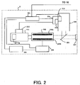
- FIG. 2 is a schematic block diagram of the laser unit 2 .
- a laser controller 201 receives the signals of the wavelength command value and the exposure dose control, etc.
- the laser controller 201 sends a high voltage signal to a high-voltage power source 202 , and a trigger signal to a compression circuit 203 at a laser emitting timing.
- the laser controller 201 sends the signal of the wavelength command value to a wavelength controller 204 .
- Discharge electrodes 205 A, 205 B are provided in a laser chamber 205 , and discharge in response to the high voltage of about 10 to 30 kV applied by the compression circuit 203 . Then, the laser gas sealed in the laser chamber 205 is excited and the laser beam oscillates.
- a light emitting part of the laser chamber 205 passes a beam splitter 206 , and enters the beam shaping optical system 3 shown in FIG. 1 through the shutter 207 . Part of the laser beam is reflected on the beam splitter 206 , and introduced into an optical monitoring part 208 .
- the laser controller 201 opens and closes a shutter 207 in accordance with a command from the main controller 16 shown in FIG. 1 .
- the optical monitoring part 208 always monitors the pulsed energy and oscillatory wavelength of the laser beam, and determines whether the measured pulsed energy is within a predetermined range around a target value.
- the laser controller 201 increases the applied voltage to the discharge electrodes 205 A and 205 B.
- the laser controller 201 decreases the applied voltage to them.
- a wavelength controller 204 compares a wavelength command value sent from the laser controller 201 with the wavelength measured by the optical monitoring part 208 , and determines whether the measured wavelength is within the predetermined range that centers on the wavelength command value.
- the optical monitoring part 208 includes an internal environment measuring means 210 , such as a barometer and a thermometer, for measuring the environment in the optical monitoring part 208 .
- the internal environment measuring means 210 can measure the refractive index to the air inside the optical monitoring part 208 .
- a band-narrowing module 211 constitutes a laser resonator with an output mirror (not shown) at the light exit part in the laser chamber 205 , and narrows a full width at half maximum of the spectral bandwidth of the laser beam down to about 0.5 pm.
- the band-narrowing module 211 drives an associative stepping motor 212 , and drives (or oscillates) the wavelength selector 211 a , such as a grating or etalon, in the band-narrowing module 211 .
- a driving unit of the wavelength selector 211 a may use a piezoelectric element.
- the wavelength controller 204 compares the wavelength command value sent from the laser controller 201 with the wavelength value measured by the optical monitoring part 208 , sends a signal to the stepping motor 212 so that the wavelength of the laser beam falls within the permissible range (or the optimization range of the wavelength by the exposure apparatus), and always controls the wavelength. Moreover, when the spectral bandwidth measured by the optical monitoring part 208 is thinner than a set value, the target value is periodically moved so as to scatter the spectral bandwidth according to the difference, and adjusts the effective spectral bandwidth to the target value. The period is adjusted to the exposure dose control period in the exposure apparatus, i.e., a pattern projection period. When the target value of the oscillatory wavelength is changed, the wavelength controller 204 drives and adjusts the stepping motor so that the oscillatory wavelength accords with the target wavelength.
- the band-narrowing module 211 implements an output of the laser beam including a wavelength spectrum S 1 that is defined by the center wavelength WL 1 and half width W 1 , as shown on the left side in FIG. 3A .
- the wavelength selector 211 a determines the center wavelength WL 1 and the wavelength spectrum S 1 .
- the wavelength spectrum S 1 varies within a predetermined variable width F 1 , but this variable width F 1 may possibly be located outside the guaranteed range of the exposure apparatus body 1 or, in particular, the projection lens 13 .
- this variable width F 1 may possibly be located outside the guaranteed range of the exposure apparatus body 1 or, in particular, the projection lens 13 .
- the mask 12 has two types of patterns, e.g., the L&S pattern 52 and isolated pattern 54 , which are formed with the same size, the pattern's CD does not become the same, and the CD 1 of the element in the L&S pattern 52 and the CD 2 of the isolated pattern 54 has a relationship of CD 1 >CD 2 as shown on the right side in FIG. 3A .
- a wavelength spectrum S 2 is wider than the first wavelength spectrum S 1 shown on the left side in FIG. 3B .
- the wavelength spectrum S 2 is formed by driving the wavelength selector 211 a and oscillating the laser beam having the wavelength spectrum S 1 shown in FIG. 3A .
- the wavelength spectrum S 2 has a center wavelength WL 2 integrated during the oscillations equal or close to the center wavelength WL 1 , and varies within a variable width F 2 (preferably, F 2 is zero) narrower than the variable width F 1 .
- variable width F 2 is within the guaranteed range of the exposure apparatus body 1 , or in particular, the projection lens 13 and the CD 1 of the element in the L&S pattern 52 and the CD 2 of the isolated pattern 54 are equal to each other or a difference between them is within a permissible range as shown on the right side in FIG. 3B .
- a width of a wave range which 95% of laser enters in the wavelength spectrum S 2 may be wider than width of a wave range which 95% of laser enters in the wavelength spectrum S 1 .
- the “width of a wave range which 95% of laser enters in the first (second) wavelength spectrum” includes a value of a center of the first (second) spectrum (or an average value), and corresponds to 2W1 (twice as large as W1), when Wav is defined as the value of the center (or the average value), and W1 is set so that 95% of the laser is included in a symmetrical range with respect to a wavelength of the value of the center, i.e., between Wav ⁇ W1 and Wav+W1.
- the present invention utilizes the fact that the spectral bandwidth W 1 of the narrowed wavelength spectrum S 1 will fall, even when slightly widened, still within the optimization range of the exposure apparatus body 1 . Therefore, according to the instant embodiment, the half width W 2 of the wavelength spectrum S 2 is within the contrast guaranteed range of the exposure apparatus body 1 .
- a relationship between the center wavelength ⁇ and the spectral width (half width W 2 ) may be set in advance as shown in FIG. 6 for the half width W 2 of the wavelength spectrum S 2 .
- the graph shown in FIG. 6 is obtained from a simulation using the spectral bandwidth that the projection lens 13 can optimize around the center wavelength ⁇ .
- An object of the instant embodiment is not to increase the spectral bandwidth from W 1 to W 2 , but to reduce the variable width of the wavelength spectrum from F 1 to F 2 so as to stabilize the wavelength spectrum.
- the main controller 16 determines the exposure parameters (step 1002 ), thereby determining the number of smoothing pulses.
- the main controller 16 sets a control periodic pulse and a measurement integral pulse (step 1004 ).
- the main controller 16 starts the exposure, and sends an oscillation signal to the laser unit 2 based on the measurement result of the barometer 15 shown in FIG. 1 (step 1006 ).
- the beam shaping optical system 3 shapes the light emitted from the laser unit 2 shown in FIG. 1 into a desired shape
- the variable ND filter 4 adjusts the light intensity of the laser beam
- the resultant laser beam enters the optical integrator 5 .
- the optical integrator 5 uniformizes the illumination light
- the condenser lens 6 condenses the light onto the masking blade 9 that is located conjugate with the mask 12 .
- the main controller 16 controls the light intensity emitted from the laser unit 2 based on the detection result from the photodetector 8 .
- the masking blade 9 illuminates the mask 12 with an optimal illumination condition via the imaging lens 10 and the mirror 11 after the illumination area is defined.
- the projection lens (or the projection optical system) 13 projects the light that passes the mask 12 onto the wafer 14 at a predetermined reduction ratio.
- the exposure apparatus of the step-and-scan manner fixes the light source 2 and the projection optical system 13 , and synchronously scans the mask 12 and the wafer 14 to expose the entire shot.
- the wafer stage (not shown) is stepped to the next shot for a new scan operation.
- the scan and step are repeated to expose multiple shots on the wafer 14 .
- the exposure apparatus of a step and repeat manner exposes while maintaining the mask 12 and the wafer 14 still.
- the wavelength controller 204 measures the spectral bandwidth on the optical monitoring part 208 (step 1008 ). Next, the wavelength controller 204 determines whether the measured spectral bandwidth is a target spectral bandwidth within the optimization range of the exposure apparatus 100 (step 1010 ). When the wavelength controller 240 determines that it is within the permissible range (step 1010 ), the laser main controller 201 continues the emissions until the main controller 16 sends an emission stop command (loop of the steps 1012 and 1008 ). Thereafter, the main controller 16 terminates the exposure (step 1014 ).
- the wavelength controller 240 determines whether the measured spectral bandwidth is thinner than the target spectral bandwidth (step 1016 ). When the wavelength controller 240 determines that it is not thinner, the main controller 16 stops the exposure and executes the error process since it cannot increase the spectral bandwidth (step 1018 ).
- the wavelength controller 240 determines that the measured spectral bandwidth is thinner than the target spectral bandwidth (step 1016 )
- the wavelength controller 240 calculates the center wavelength oscillatory width using the evaluation function (step 1020 ).
- the wavelength controller 240 executes the center wavelength control in addition to the center wavelength control (step 1022 ). The procedure moves to the step 1012 after the step 1022 .
- the exposure apparatus 100 uses the (integrated) laser beam whose variable width is maintained within the permissible range, thus controls resolvable sizes of various patterns, such as a L&S pattern and an isolated pattern, transfers a pattern onto the resist with high precision, and provides high-quality devices (such as a semiconductor device, an LCD device, an image pickup device (such as a CCD), and a thin-film magnetic head).
- various patterns such as a L&S pattern and an isolated pattern
- high-quality devices such as a semiconductor device, an LCD device, an image pickup device (such as a CCD), and a thin-film magnetic head.
- the present invention is not limited to a case where the exposure apparatus body 1 cannot maintain the variable width F 1 . Even if it can maintain the variable width F 1 , the reduced variable width would preferably provide the process with a larger degree of freedom, such as a larger DOF. Thereby, the process becomes so easy that a less expensive wafer can be used.
- the wavelength controller 204 sets the oscillatory period to a control period at which the main controller 16 uses as the timing to projecting the pattern.
- the target center wavelength of the ordinate axis is WL 2 and the abscissa axis is the control period determined by the projection lens 13 . It is enough that the control period is an n-fold oscillatory period.
- the wavelength spectrum changing method of the instant embodiment is effective to an approximate equalization between the CD of the L&S pattern 52 's element and the CD of the isolated pattern 54 , but the present invention is not limited to this embodiment.
- the wavelength spectrum changing method of the instant embodiment is effective even in intentionally changing their CDS.
- the spectral bandwidth corresponding to it can be selected.
- a necessity to intentionally create a difference between their CDs arises, for example, when an originally intended wafer and resist are not used.
- a time period for which the laser beam is irradiated onto one point on the object, such as a wafer is substantially an integer multiple of the oscillating or driving period of the wavelength selector (the predetermined period).
- T1 is a time period for which the laser beam is irradiated onto one point on the object
- T2 is the predetermined time period
- the following conditions are preferably met: (n 0.1)T2 ⁇ T1 ⁇ (n0.1)T2 (n: natural number) [EQUATION 1] (n ⁇ 0.01)T2 ⁇ T1 ⁇ (n+0.01)T2 (n: natural number) [EQUATION2]
- FIG. 8 is a flowchart for explaining a fabrication of devices (i.e., semiconductor chips such as IC and LSI, LCDS, CCDS, etc.).
- a fabrication of a semiconductor chip as an example.
- Step 1 circuit design
- Step 2 mask fabrication
- Step 3 wafer making
- Step 4 wafer process
- a pretreatment forms actual circuitry on the wafer through photolithography using the mask and wafer.
- Step 5 which is also referred to as a post-treatment, forms into a semiconductor chip tho wafer formed in Step 4 and includes an assembly step (e.g., dicing, bonding), a packaging step (chip sealing), and the like.
- Step 6 performs various tests for the semiconductor device made in Step 5 , such as a validity test and a durability test. Through these steps, a semiconductor device is finished and shipped (Step 7 ).
- FIG. 9 is a detailed flowchart of the wafer process in Step 4 .
- Step 11 oxidation
- Step 12 CVD
- Step 13 electrode formation
- Step 14 ion implantation
- Step 15 resist process
- Step 16 exposure
- Step 17 development
- Step 18 etching
- Step 19 resist stripping
- the device fabrication method of this embodiment may manufacture higher quality devices than the conventional one.
- the device fabrication method using the exposure apparatus, and the devices as finished goods also constitute one aspect of the present invention.
- the present invention covers devices as intermediate and final products. Such devices include semiconductor chips like an LSI and VLSI, CCDs, LCDs, magnetic sensors, thin film magnetic heads, and the like.
- the present invention can provide a laser unit, and an exposure method and apparatus using the same, and a device manufacturing method, for the stable spectral bandwidth and the high-quality exposure.
Landscapes
- Physics & Mathematics (AREA)
- Electromagnetism (AREA)
- General Physics & Mathematics (AREA)
- Engineering & Computer Science (AREA)
- Plasma & Fusion (AREA)
- Optics & Photonics (AREA)
- Exposure And Positioning Against Photoresist Photosensitive Materials (AREA)
- Lasers (AREA)
- Exposure Of Semiconductors, Excluding Electron Or Ion Beam Exposure (AREA)
Applications Claiming Priority (2)
| Application Number | Priority Date | Filing Date | Title |
|---|---|---|---|
| JP2003-434733 | 2003-12-26 | ||
| JP2003434733A JP2005191503A (ja) | 2003-12-26 | 2003-12-26 | レーザ装置、露光方法及び装置 |
Publications (1)
| Publication Number | Publication Date |
|---|---|
| US20050190801A1 true US20050190801A1 (en) | 2005-09-01 |
Family
ID=34545111
Family Applications (1)
| Application Number | Title | Priority Date | Filing Date |
|---|---|---|---|
| US11/022,399 Abandoned US20050190801A1 (en) | 2003-12-26 | 2004-12-23 | Laser unit, exposure apparatus and method |
Country Status (3)
| Country | Link |
|---|---|
| US (1) | US20050190801A1 (enExample) |
| EP (1) | EP1548501A3 (enExample) |
| JP (1) | JP2005191503A (enExample) |
Cited By (6)
| Publication number | Priority date | Publication date | Assignee | Title |
|---|---|---|---|---|
| US20060170899A1 (en) * | 2004-12-23 | 2006-08-03 | Asml Netherlands B.V. | Lithographic apparatus, excimer laser and device manufacturing method |
| US20070296945A1 (en) * | 2006-03-17 | 2007-12-27 | Canon Kabushiki Kaisha | Exposure apparatus and image plane detecting method |
| US20080169862A1 (en) * | 2007-01-12 | 2008-07-17 | Samsung Electronics Co., Ltd. | Semiconductor device and methods for controlling its patterns |
| US7477356B2 (en) | 2006-06-09 | 2009-01-13 | Canon Kabushiki Kaisha | Exposure apparatus |
| US20090147231A1 (en) * | 2007-12-06 | 2009-06-11 | Canon Kabushiki Kaisha | Scanning exposure apparatus and method of manufacturing device |
| US20150070673A1 (en) * | 2013-06-11 | 2015-03-12 | Cymer, Llc | Wafer-based light source parameter control |
Citations (15)
| Publication number | Priority date | Publication date | Assignee | Title |
|---|---|---|---|---|
| US4905041A (en) * | 1987-10-19 | 1990-02-27 | Canon Kabushiki Kaisha | Exposure apparatus |
| US5010230A (en) * | 1989-07-24 | 1991-04-23 | Nikon Corporation | Laser processor |
| US5191374A (en) * | 1988-11-17 | 1993-03-02 | Nikon Corporation | Exposure control apparatus |
| US5343270A (en) * | 1990-10-30 | 1994-08-30 | Nikon Corporation | Projection exposure apparatus |
| US5450436A (en) * | 1992-11-20 | 1995-09-12 | Kabushiki Kaisha Komatsu Seisakusho | Laser gas replenishing apparatus and method in excimer laser system |
| US5748316A (en) * | 1993-10-20 | 1998-05-05 | Komatsu, Ltd. | Detector for wavelength of excimer laser |
| US6078599A (en) * | 1997-07-22 | 2000-06-20 | Cymer, Inc. | Wavelength shift correction technique for a laser |
| US6252647B1 (en) * | 1990-11-15 | 2001-06-26 | Nikon Corporation | Projection exposure apparatus |
| US20010036207A1 (en) * | 2000-04-26 | 2001-11-01 | Yashiyuki Nagai | Laser oscillation apparatus, exposure apparatus, semiconductor device manufacturing method, semiconductor manufacturing factory, and exposure apparatus maintenance method |
| US6456760B1 (en) * | 1996-09-02 | 2002-09-24 | Nippon Telegraph And Telephone Corporation | Optical signal processing apparatus and optical signal processing method |
| US6496528B2 (en) * | 1999-09-03 | 2002-12-17 | Cymer, Inc. | Line narrowing unit with flexural grating mount |
| US6526086B1 (en) * | 1997-05-09 | 2003-02-25 | Komatsu Ltd. | Band narrowing laser |
| US6529531B1 (en) * | 1997-07-22 | 2003-03-04 | Cymer, Inc. | Fast wavelength correction technique for a laser |
| US6721340B1 (en) * | 1997-07-22 | 2004-04-13 | Cymer, Inc. | Bandwidth control technique for a laser |
| US20040233403A1 (en) * | 2001-09-21 | 2004-11-25 | Detlef Gerhard | Device and method for optically scanning a substrate disk |
-
2003
- 2003-12-26 JP JP2003434733A patent/JP2005191503A/ja not_active Withdrawn
-
2004
- 2004-12-22 EP EP04030471A patent/EP1548501A3/en not_active Withdrawn
- 2004-12-23 US US11/022,399 patent/US20050190801A1/en not_active Abandoned
Patent Citations (15)
| Publication number | Priority date | Publication date | Assignee | Title |
|---|---|---|---|---|
| US4905041A (en) * | 1987-10-19 | 1990-02-27 | Canon Kabushiki Kaisha | Exposure apparatus |
| US5191374A (en) * | 1988-11-17 | 1993-03-02 | Nikon Corporation | Exposure control apparatus |
| US5010230A (en) * | 1989-07-24 | 1991-04-23 | Nikon Corporation | Laser processor |
| US5343270A (en) * | 1990-10-30 | 1994-08-30 | Nikon Corporation | Projection exposure apparatus |
| US6252647B1 (en) * | 1990-11-15 | 2001-06-26 | Nikon Corporation | Projection exposure apparatus |
| US5450436A (en) * | 1992-11-20 | 1995-09-12 | Kabushiki Kaisha Komatsu Seisakusho | Laser gas replenishing apparatus and method in excimer laser system |
| US5748316A (en) * | 1993-10-20 | 1998-05-05 | Komatsu, Ltd. | Detector for wavelength of excimer laser |
| US6456760B1 (en) * | 1996-09-02 | 2002-09-24 | Nippon Telegraph And Telephone Corporation | Optical signal processing apparatus and optical signal processing method |
| US6526086B1 (en) * | 1997-05-09 | 2003-02-25 | Komatsu Ltd. | Band narrowing laser |
| US6078599A (en) * | 1997-07-22 | 2000-06-20 | Cymer, Inc. | Wavelength shift correction technique for a laser |
| US6529531B1 (en) * | 1997-07-22 | 2003-03-04 | Cymer, Inc. | Fast wavelength correction technique for a laser |
| US6721340B1 (en) * | 1997-07-22 | 2004-04-13 | Cymer, Inc. | Bandwidth control technique for a laser |
| US6496528B2 (en) * | 1999-09-03 | 2002-12-17 | Cymer, Inc. | Line narrowing unit with flexural grating mount |
| US20010036207A1 (en) * | 2000-04-26 | 2001-11-01 | Yashiyuki Nagai | Laser oscillation apparatus, exposure apparatus, semiconductor device manufacturing method, semiconductor manufacturing factory, and exposure apparatus maintenance method |
| US20040233403A1 (en) * | 2001-09-21 | 2004-11-25 | Detlef Gerhard | Device and method for optically scanning a substrate disk |
Cited By (14)
| Publication number | Priority date | Publication date | Assignee | Title |
|---|---|---|---|---|
| US8089613B2 (en) | 2004-12-23 | 2012-01-03 | Asml Netherlands B.V. | Lithographic apparatus, excimer laser and device manufacturing method |
| US9316924B2 (en) | 2004-12-23 | 2016-04-19 | Asml Netherlands B.V. | Lithographic apparatus, excimer laser and device manufacturing method |
| US20100329290A1 (en) * | 2004-12-23 | 2010-12-30 | Asml Netherlands B.V. | Lithographic apparatus, excimer laser and device manufacturing method |
| US7817247B2 (en) * | 2004-12-23 | 2010-10-19 | Asml Netherlands B.V. | Lithographic apparatus, excimer laser and device manufacturing method |
| US20060170899A1 (en) * | 2004-12-23 | 2006-08-03 | Asml Netherlands B.V. | Lithographic apparatus, excimer laser and device manufacturing method |
| US7656503B2 (en) | 2006-03-17 | 2010-02-02 | Canon Kabushiki Kaisha | Exposure apparatus and image plane detecting method |
| US20070296945A1 (en) * | 2006-03-17 | 2007-12-27 | Canon Kabushiki Kaisha | Exposure apparatus and image plane detecting method |
| US7477356B2 (en) | 2006-06-09 | 2009-01-13 | Canon Kabushiki Kaisha | Exposure apparatus |
| US20080169862A1 (en) * | 2007-01-12 | 2008-07-17 | Samsung Electronics Co., Ltd. | Semiconductor device and methods for controlling its patterns |
| US20090147231A1 (en) * | 2007-12-06 | 2009-06-11 | Canon Kabushiki Kaisha | Scanning exposure apparatus and method of manufacturing device |
| US7826036B2 (en) | 2007-12-06 | 2010-11-02 | Canon Kabushiki Kaisha | Scanning exposure apparatus and method of manufacturing device |
| US9715180B2 (en) * | 2013-06-11 | 2017-07-25 | Cymer, Llc | Wafer-based light source parameter control |
| US20150070673A1 (en) * | 2013-06-11 | 2015-03-12 | Cymer, Llc | Wafer-based light source parameter control |
| US10036960B2 (en) | 2013-06-11 | 2018-07-31 | Cymer, Llc | Wafer-based light source parameter control |
Also Published As
| Publication number | Publication date |
|---|---|
| JP2005191503A (ja) | 2005-07-14 |
| EP1548501A3 (en) | 2005-07-06 |
| EP1548501A2 (en) | 2005-06-29 |
Similar Documents
| Publication | Publication Date | Title |
|---|---|---|
| US6727976B2 (en) | Exposure apparatus with a pulsed laser | |
| US6975387B2 (en) | Wavefront aberration measuring instrument, wavefront aberration measuring method, exposure apparatus, and method for manufacturing micro device | |
| KR101302244B1 (ko) | 노광 장치, 노광 방법 및 디바이스 제조 방법, 및 시스템 | |
| US7123346B2 (en) | Projection exposure apparatus with line width calculator controlled diaphragm unit | |
| US7154922B2 (en) | Laser beam source control method and unit, exposure method and apparatus, and device manufacturing method | |
| KR20180129625A (ko) | 결정방법, 노광방법, 정보 처리장치, 프로그램 및 물품의 제조방법 | |
| JP2009141154A (ja) | 走査露光装置及びデバイス製造方法 | |
| KR100873538B1 (ko) | 노광장치 및 디바이스의 제조 방법 | |
| US7498596B2 (en) | Exposure method that obtains, prior to exposure, reticle surface form data and measurement position error, for scanning control | |
| US7085302B2 (en) | Laser apparatus, exposure apparatus and method | |
| JP3363532B2 (ja) | 走査型露光装置 | |
| US20050190801A1 (en) | Laser unit, exposure apparatus and method | |
| JP4208532B2 (ja) | 光学素子の透過率を測定する方法 | |
| KR20080050305A (ko) | 노광장치 및 디바이스의 제조방법 | |
| US6493066B1 (en) | Exposure apparatus | |
| US6744492B2 (en) | Exposure apparatus | |
| US7486379B2 (en) | Exposure apparatus, method applied to the apparatus, and device manufacturing method | |
| JP2002198281A (ja) | 照明装置及びそれを用いた露光装置 | |
| US5878068A (en) | Energy quantity control method | |
| JP2003298163A (ja) | レーザー装置、露光装置及び露光方法 | |
| JP4829429B2 (ja) | 透過率測定装置 | |
| US20020191172A1 (en) | Laser output control method, laser apparatus and exposure apparatus | |
| JP2003014643A (ja) | 透過率測定装置、並びに露光装置 | |
| JPH08306619A (ja) | 露光装置及びそれを用いたデバイスの製造方法 | |
| JP2003282430A (ja) | 露光装置及び露光方法、デバイス製造方法、並びに測定方法及び測定装置 |
Legal Events
| Date | Code | Title | Description |
|---|---|---|---|
| AS | Assignment |
Owner name: CANON KABUSHIKI KAISHA, JAPAN Free format text: ASSIGNMENT OF ASSIGNORS INTEREST;ASSIGNORS:SUKEGAWA, TAKASHI;TAKAHASHI, KAZUHIRO;REEL/FRAME:016579/0318 Effective date: 20050203 |
|
| STCB | Information on status: application discontinuation |
Free format text: ABANDONED -- FAILURE TO RESPOND TO AN OFFICE ACTION |