US20030197587A1 - Solid-state inductor and method for same - Google Patents
Solid-state inductor and method for same Download PDFInfo
- Publication number
- US20030197587A1 US20030197587A1 US10/131,411 US13141102A US2003197587A1 US 20030197587 A1 US20030197587 A1 US 20030197587A1 US 13141102 A US13141102 A US 13141102A US 2003197587 A1 US2003197587 A1 US 2003197587A1
- Authority
- US
- United States
- Prior art keywords
- thin film
- cmr
- inductor
- bias voltage
- forming
- Prior art date
- Legal status (The legal status is an assumption and is not a legal conclusion. Google has not performed a legal analysis and makes no representation as to the accuracy of the status listed.)
- Granted
Links
Images


Classifications
-
- G—PHYSICS
- G11—INFORMATION STORAGE
- G11C—STATIC STORES
- G11C13/00—Digital stores characterised by the use of storage elements not covered by groups G11C11/00, G11C23/00, or G11C25/00
- G11C13/0002—Digital stores characterised by the use of storage elements not covered by groups G11C11/00, G11C23/00, or G11C25/00 using resistive RAM [RRAM] elements
- G11C13/0007—Digital stores characterised by the use of storage elements not covered by groups G11C11/00, G11C23/00, or G11C25/00 using resistive RAM [RRAM] elements comprising metal oxide memory material, e.g. perovskites
-
- H—ELECTRICITY
- H01—ELECTRIC ELEMENTS
- H01F—MAGNETS; INDUCTANCES; TRANSFORMERS; SELECTION OF MATERIALS FOR THEIR MAGNETIC PROPERTIES
- H01F27/00—Details of transformers or inductances, in general
- H01F27/24—Magnetic cores
- H01F27/245—Magnetic cores made from sheets, e.g. grain-oriented
-
- H—ELECTRICITY
- H10—SEMICONDUCTOR DEVICES; ELECTRIC SOLID-STATE DEVICES NOT OTHERWISE PROVIDED FOR
- H10D—INORGANIC ELECTRIC SEMICONDUCTOR DEVICES
- H10D1/00—Resistors, capacitors or inductors
- H10D1/20—Inductors
-
- H—ELECTRICITY
- H10—SEMICONDUCTOR DEVICES; ELECTRIC SOLID-STATE DEVICES NOT OTHERWISE PROVIDED FOR
- H10D—INORGANIC ELECTRIC SEMICONDUCTOR DEVICES
- H10D84/00—Integrated devices formed in or on semiconductor substrates that comprise only semiconducting layers, e.g. on Si wafers or on GaAs-on-Si wafers
-
- G—PHYSICS
- G11—INFORMATION STORAGE
- G11C—STATIC STORES
- G11C2213/00—Indexing scheme relating to G11C13/00 for features not covered by this group
- G11C2213/30—Resistive cell, memory material aspects
- G11C2213/31—Material having complex metal oxide, e.g. perovskite structure
-
- H—ELECTRICITY
- H01—ELECTRIC ELEMENTS
- H01F—MAGNETS; INDUCTANCES; TRANSFORMERS; SELECTION OF MATERIALS FOR THEIR MAGNETIC PROPERTIES
- H01F10/00—Thin magnetic films, e.g. of one-domain structure
- H01F10/08—Thin magnetic films, e.g. of one-domain structure characterised by magnetic layers
- H01F10/10—Thin magnetic films, e.g. of one-domain structure characterised by magnetic layers characterised by the composition
- H01F10/18—Thin magnetic films, e.g. of one-domain structure characterised by magnetic layers characterised by the composition being compounds
- H01F10/193—Magnetic semiconductor compounds
-
- H—ELECTRICITY
- H01—ELECTRIC ELEMENTS
- H01F—MAGNETS; INDUCTANCES; TRANSFORMERS; SELECTION OF MATERIALS FOR THEIR MAGNETIC PROPERTIES
- H01F21/00—Variable inductances or transformers of the signal type
-
- H—ELECTRICITY
- H01—ELECTRIC ELEMENTS
- H01F—MAGNETS; INDUCTANCES; TRANSFORMERS; SELECTION OF MATERIALS FOR THEIR MAGNETIC PROPERTIES
- H01F41/00—Apparatus or processes specially adapted for manufacturing or assembling magnets, inductances or transformers; Apparatus or processes specially adapted for manufacturing materials characterised by their magnetic properties
- H01F41/14—Apparatus or processes specially adapted for manufacturing or assembling magnets, inductances or transformers; Apparatus or processes specially adapted for manufacturing materials characterised by their magnetic properties for applying magnetic films to substrates
- H01F41/24—Apparatus or processes specially adapted for manufacturing or assembling magnets, inductances or transformers; Apparatus or processes specially adapted for manufacturing materials characterised by their magnetic properties for applying magnetic films to substrates from liquids
-
- Y—GENERAL TAGGING OF NEW TECHNOLOGICAL DEVELOPMENTS; GENERAL TAGGING OF CROSS-SECTIONAL TECHNOLOGIES SPANNING OVER SEVERAL SECTIONS OF THE IPC; TECHNICAL SUBJECTS COVERED BY FORMER USPC CROSS-REFERENCE ART COLLECTIONS [XRACs] AND DIGESTS
- Y10—TECHNICAL SUBJECTS COVERED BY FORMER USPC
- Y10T—TECHNICAL SUBJECTS COVERED BY FORMER US CLASSIFICATION
- Y10T29/00—Metal working
- Y10T29/49—Method of mechanical manufacture
- Y10T29/49002—Electrical device making
- Y10T29/4902—Electromagnet, transformer or inductor
Definitions
- This invention generally relates to semiconductor fabrication and, more particularly, to a solid-state inductor for analog integrated circuit (IC) fabrication and a method for processing the same.
- an IC integrated inductor is formed from a metal line, designed in spiral form, overlying a thick layer of insulator on silicon substrate.
- the inductance value of an inductor so formed is very low, so that the formation of a practical inductor requires a large silicon area.
- the large-sized inductors generate parasitic reactances and unintended mutual inductances with components that are adjacent, overlying, or underlying the inductor.
- a conventional inductor is a passive component, meaning that once it is formed in the IC, the inductance value cannot be changed. Thus, the inductor cannot be used for frequency tuning. Frequency tuning would be desirable in the fabrication of circuits such as filters, antennas, and oscillators, to name a few of examples.
- the present invention describes a solid-state inductor, which has a relatively high inductance value, requires a very small area, and is suitable to be integrated into the conventional integrated circuits, whether it is a CMOS or a Bipolar circuit fabricated on silicon, or on compound semiconductor substrate.
- a method for forming a solid-state inductor comprises: forming a bottom electrode; forming a colossal magnetoresistance (CMR) thin film overlying the bottom electrode; forming a top electrode overlying the CMR thin film; applying an electrical field treatment to the CMR thin film in the range of 0.4 to 1 megavolts per centimeter (MV/cm) with a pulse width in the range of 100 nanoseconds to 1 millisecond; in response to the electrical field treatment, converting the CMR thin film into a CMR thin film inductor; applying a bias voltage between the top and bottom electrodes; and, in response to the applied bias voltage, creating an inductance between the top and bottom electrodes.
- the applied bias voltage is varied, the inductance varies in response.
- the CMR thin film overlying the bottom electrode includes using a material such as Pr 0.3 Ca 0.7 MnO 3 (PCMO), La 0.7 Ca 0.3 MnO 3 (LCMO), Y 1-x Ca x MnO 3 (YCMO), or high-temperature super conductor (HTSC) materials with a film thickness of approximately 2000 ⁇ .
- Forming the CMR thin film overlying the bottom electrode includes: spincoating a first layer having a thickness of approximately 670 ⁇ ; annealing the first layer at a temperature of approximately 650 degrees C.
- FIG. 1 is a diagram of the present invention solid-state inductor.
- FIG. 2 illustrates the present invention solid-state inductor in a couple of practical IC applications.
- FIG. 3 illustrates the reactance of an exemplary CMR film, before electric field treatment.
- FIG. 4 illustrates the reactance of the exemplary CMR film after electric field treatment.
- FIG. 5 is a flowchart illustrating the present invention method for forming a solid-state inductor.
- FIG. 1 is a diagram of the present invention solid-state inductor.
- the inductor 100 comprises a bottom electrode 102 and an electric field-treated colossal magnetoresistance (CMR) thin film 104 overlying the bottom electrode 102 .
- a top electrode 106 overlies the CMR thin film 104 .
- CMR colossal magnetoresistance
- the CMR thin film 104 is made from a material such as Pr 0.3 Ca 0.7 MnO 3 (PCMO), La 0.7 Ca 0.3 MnO 3 (LCMO), Y 1-x Ca x MnO 3 (YCMO), or high-temperature super conductor (HTSC) materials. However, other equivalent materials might also be practical, depending upon requirements.
- the CMR thin film 104 has a thickness 108 of approximately 2000 ⁇ .
- the CMR thin film 104 has been previously exposed to an electric field in the range of 0.4 to 1 megavolts per centimeter (MV/cm), with a pulse width in the range of 100 nanoseconds (ns) to 1 millisecond (ms).
- MV/cm megavolts per centimeter
- ns nanoseconds
- ms millisecond
- the bottom electrode 102 is made from a material such as Al, Au, Ti, Ta, Pt, Al, Cu, W, Ir, AlSi, or other noble metals. However, other conductors, well known in the fabrication of ICs could also be used. Likewise, the top electrode 106 is typically made from a material selected from the group including Al, Au, Ti, Ta, Pt, Al, Cu, W, Ir, AlSi, or other noble metals.
- a means for applying a bias voltage between the top and bottom electrodes is shown, represented by reference designator 112 .
- the solid-state inductor 100 is part of a larger, more complex circuit, and the bias voltage and relative ground are connections through other components, such as transistors, not shown.
- An inductance, or inductance value (L), represented by reference designator 114 is created between the top and bottom electrodes 106 / 102 in response to the applied bias voltage.
- the voltage applying means 112 varies the applied bias voltage.
- the inductance 110 between the top and bottom electrodes 106 / 102 varies in response to variances in the applied bias voltage.
- Some practical bias voltage ranges have been developed as examples.
- the bias applying means 112 applies a voltage between the top and bottom electrodes 106 / 102 within the range of either 0.5 to 5 dc volts, or ⁇ 0.5 to ⁇ 5 dc volts.
- an ac voltage can also be used.
- other dc voltage ranges can be used for different variations of CMR material, CMR volume, and the electric field treatments.
- the inductance 114 between the top and bottom electrodes 106 / 102 can be in the range of less than 0.01 micro-Henrys ( ⁇ H) to greater than 1 ⁇ H, depending on bias voltage, the CMR material, and the geometries (volume, diameter, and thickness) of the CMR thin film 104 .
- the inductance 114 between the top and bottom electrodes 106 / 102 is a maximum value in response to an applied voltage of either +1 dc volt or ⁇ 1 dc volt. Again however, the relationship between maximum inductance and bias voltage is dependent upon CMR material and CMR geometries.
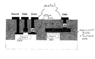
- FIG. 2 illustrates the present invention solid-state inductor 100 in a couple of practical IC applications.
- the present invention solidstate inductor is a two terminal pillar structure. It can be fabricated into a single via hole with bottom electrode onto a pn junction, or on a local interconnect metal line.
- the inductor can be integrated to the IC after the completion of the front end of processing as is illustrated in FIG. 2.
- the inductor 100 is integrated to a drain junction 202 .
- the inductor 100 is integrated to a gate electrode 206 .
- the inductor(s) 100 can be deposited onto the semiconductor substrate using conventional deposition methods, such as spin coating, sputtering and CVD process.
- the solid-state inductor has very high inductance that, using a bias voltage control, can vary more than two orders of magnitudes.
- the tuning of any LC circuit, of which the inductor 100 is a part, can be achieved by adjusting the bias voltage across the inductor 100 .
- a present invention inductor can be made using a colossal magnetoresistance (CMR) thin film resistor, fabricated using a spin-coating process.
- the CMR material can be PCMO (Pr 0.3 Ca 0.7 MnO 3 ).
- the film is coated three times for a total thickness of about 200 nm onto Platinum substrate.
- the film is annealed at 650° C. for 30 minutes after a first coating, and annealed at 550° C. for 30 minutes after the second and the third coatings.
- the top electrode is also Platinum, although some other metals such as Al, Cu, W, Ir, AlSi, or other noble metals may also be used.
- the impedance of the as-fabricated film is a measured having resistance and capacitance components.
- FIG. 3 illustrates the reactance of an exemplary CMR film, before electric field treatment. All measurements are of resistance in series with inductance. The measurement frequency is 1 MHz. The measured inductance shown is negative and, therefore, capacitive. The figure also shows that the capacitance and the resistance of this thin film is practically independent of voltage in the given measurement region.
- FIG. 4 illustrates the reactance of the exemplary CMR film after electric field treatment.
- the property of the impedance changes drastically after an electric field of 0.4 MV/cm to 1 MV/cm is applied to the CMR film.
- the resistance of the CMR film decreases from about 275 Ohms to lower than 20 Ohm.
- the CMR film becomes inductive in response to bias voltages of ⁇ 5V to ⁇ 0.5V, or 0.5V to 5V. Outside of these bias voltage ranges, the reactance of the CMR film is capacitance.
- the maximum inductance is more than 1 ⁇ H.
- the inductance of the PCMO solid-state inductor can be varied by more than two orders of magnitude by changing the voltage applied to the device. From the nature of the material, it is expected that colossal magnetoresistance (CMR) and high temperature super conductor (HTSC) material are practical for electrically tunable solid-state inductor fabrication. The device area determines the magnitude of the inductance.
- CMR colossal magnetoresistance
- HTSC high temperature super conductor
- the solid-state electrically tunable inductor is suitable as a build-in element for filters and antennas of any integrated circuit.
- FIG. 5 is a flowchart illustrating the present invention method for forming a solid-state inductor. Although this method is depicted as a sequence of numbered steps for clarity, no order should be inferred from the numbering unless explicitly stated. It should be understood that some of these steps may be skipped, performed in parallel, or performed without the requirement of maintaining a strict order of sequence.
- the methods start at Step 500 .
- Step 502 forms a bottom electrode.
- Step 504 forms a colossal magnetoresistance (CMR) thin film overlying the bottom electrode.
- Step 506 forms a top electrode overlying the CMR thin film.
- Step 508 applies an electrical field treatment to the CMR thin film. Alternately, Step 508 applies an electric field while simultaneously annealing the CMR thin film.
- Step 510 in response to the electrical field treatment, converts the CMR thin film into a CMR thin film inductor.
- Step 512 applies a bias voltage between the top and bottom electrodes.
- Step 514 in response to the applied bias voltage, creates an inductance between the top and bottom electrodes.
- Step 516 varies the applied bias voltage.
- Step 518 varies the inductance in response to variances in the applied bias voltage.
- Forming a CMR thin film overlying the bottom electrode in Step 504 includes using a material such as Pr 0.3 Ca 0.7 MnO 3 (PCMO), La 0.7 Ca 0.3 MnO 3 (LCMO), Y 1-x Ca x MnO 3 (YCMO), or high-temperature super conductor (HTSC) materials.
- PCMO Pr 0.3 Ca 0.7 MnO 3
- LCMO La 0.7 Ca 0.3 MnO 3
- YCMO Y 1-x Ca x MnO 3
- HTSC high-temperature super conductor
- Step 504 forming a CMR thin film overlying the bottom electrode in Step 504 includes substeps.
- Step 504 a spin-coats a first layer having a thickness of approximately 670 ⁇ .
- Step 504 b anneals the first layer at a temperature of approximately 650 degrees C. for a period of approximately 30 minutes.
- Step 504 c spin-coats a second layer, having a thickness of approximately 670 ⁇ , overlying the first layer.
- Step 504 d anneals the second layer at a temperature of approximately 550 degrees C. for a period of approximately 30 minutes.
- Step 504 e spin-coats a third layer, having a thickness of approximately 670 ⁇ , overlying the second layer.
- Step 504 f anneals the third layer at a temperature of approximately 550 degrees C. for a period of approximately 30 minutes.
- forming a bottom electrode in Step 502 includes forming a bottom electrode from a material such as Al, Au, Ti, Ta, Pt, Al, Cu, W, Ir, AlSi, or other noble metals.
- forming a top electrode in Step 506 includes forming a top electrode from a material such as Al, Au, Ti, Ta, Pt, Al, Cu, W, Ir, AlSi, or other noble metals.
- applying an electrical field treatment to the CMR thin film in Step 508 includes applying an electric field in the range of 0.4 to 1 megavolts per centimeter (MV/cm) with a pulse width in the range of 100 ns to 1 ms.
- MV/cm megavolts per centimeter
- applying a bias voltage between the top and bottom electrodes in Step 512 includes applying a bias voltage between the top and bottom electrodes of either a dc voltage within the range of 0.5 to 5 volts, or a dc voltage within the range of ⁇ 0.5 to ⁇ 5 volts.
- Creating an inductance between the top and bottom electrodes in Step 514 includes creating an inductance in the range of less than 0.01 micro-Henry ( ⁇ H) to greater than 1 ⁇ H.
- varying the inductance between the top and bottom electrodes in response to variances in the applied bias voltage in Step 518 includes creating the maximum inductance at a bias voltage of either approximately +1 dc volt, or approximately ⁇ 1 dc volt.
- a solid-state inductor and solid-state inductor fabrication method have been provided. A few practical inductor applications have been provided as examples. However, the present invention solid-state inductor has wider application than merely these examples. Likewise, a exemplary fabrication process has been given, but the solid-state inductor could be fabricated using equivalent processes and materials. Other variations and embodiments of the invention will occur to those skilled in the art.
Landscapes
- Engineering & Computer Science (AREA)
- Chemical & Material Sciences (AREA)
- Materials Engineering (AREA)
- Power Engineering (AREA)
- Hall/Mr Elements (AREA)
- Coils Or Transformers For Communication (AREA)
- Semiconductor Integrated Circuits (AREA)
Abstract
Description
- 1. Field of the Invention
- This invention generally relates to semiconductor fabrication and, more particularly, to a solid-state inductor for analog integrated circuit (IC) fabrication and a method for processing the same.
- 2. Description of the Related Art
- Conventionally, an IC integrated inductor is formed from a metal line, designed in spiral form, overlying a thick layer of insulator on silicon substrate. The inductance value of an inductor so formed is very low, so that the formation of a practical inductor requires a large silicon area. Besides using a great amount of valuable IC area, the large-sized inductors generate parasitic reactances and unintended mutual inductances with components that are adjacent, overlying, or underlying the inductor.
- Further, a conventional inductor is a passive component, meaning that once it is formed in the IC, the inductance value cannot be changed. Thus, the inductor cannot be used for frequency tuning. Frequency tuning would be desirable in the fabrication of circuits such as filters, antennas, and oscillators, to name a few of examples.
- It would be advantageous if an IC inductor could be made smaller, with a greater inductance value.
- It would be advantageous if the inductance value of an IC inductor could be varied or tuned in an IC circuit.
- The present invention describes a solid-state inductor, which has a relatively high inductance value, requires a very small area, and is suitable to be integrated into the conventional integrated circuits, whether it is a CMOS or a Bipolar circuit fabricated on silicon, or on compound semiconductor substrate.
- Accordingly, a method is provided for forming a solid-state inductor. The method comprises: forming a bottom electrode; forming a colossal magnetoresistance (CMR) thin film overlying the bottom electrode; forming a top electrode overlying the CMR thin film; applying an electrical field treatment to the CMR thin film in the range of 0.4 to 1 megavolts per centimeter (MV/cm) with a pulse width in the range of 100 nanoseconds to 1 millisecond; in response to the electrical field treatment, converting the CMR thin film into a CMR thin film inductor; applying a bias voltage between the top and bottom electrodes; and, in response to the applied bias voltage, creating an inductance between the top and bottom electrodes. When the applied bias voltage is varied, the inductance varies in response.
- The CMR thin film overlying the bottom electrode includes using a material such as Pr 0.3Ca0.7MnO3 (PCMO), La0.7Ca0.3MnO3 (LCMO), Y1-xCaxMnO3 (YCMO), or high-temperature super conductor (HTSC) materials with a film thickness of approximately 2000 Å. Forming the CMR thin film overlying the bottom electrode includes: spincoating a first layer having a thickness of approximately 670 Å; annealing the first layer at a temperature of approximately 650 degrees C. for a period of approximately 30 minutes; spin-coating a second layer, having a thickness of approximately 670 Å, overlying the first layer; annealing the second layer at a temperature of approximately 550 degrees C. for a period of approximately 30 minutes; spin-coating a third layer, having a thickness of approximately 670 Å, overlying the second layer; and, annealing the third layer at a temperature of approximately 550 degrees C. for a period of approximately 30 minutes.
- Additional details of the above-described method, and a solid-state inductor device are presented below.
- FIG. 1 is a diagram of the present invention solid-state inductor.
- FIG. 2 illustrates the present invention solid-state inductor in a couple of practical IC applications.
- FIG. 3 illustrates the reactance of an exemplary CMR film, before electric field treatment.
- FIG. 4 illustrates the reactance of the exemplary CMR film after electric field treatment.
- FIG. 5 is a flowchart illustrating the present invention method for forming a solid-state inductor.
- FIG. 1 is a diagram of the present invention solid-state inductor. The
inductor 100 comprises abottom electrode 102 and an electric field-treated colossal magnetoresistance (CMR)thin film 104 overlying thebottom electrode 102. Atop electrode 106 overlies the CMRthin film 104. - The CMR
thin film 104 is made from a material such as Pr0.3Ca0.7MnO3 (PCMO), La0.7Ca0.3MnO3 (LCMO), Y1-xCaxMnO3 (YCMO), or high-temperature super conductor (HTSC) materials. However, other equivalent materials might also be practical, depending upon requirements. The CMRthin film 104 has a thickness 108 of approximately 2000 Å. - As explained in more detail below, the CMR
thin film 104 has been previously exposed to an electric field in the range of 0.4 to 1 megavolts per centimeter (MV/cm), with a pulse width in the range of 100 nanoseconds (ns) to 1 millisecond (ms). This is just an exemplary treatment. Other means of treatment are practical and depend upon the CMR material, intervening materials, and the desired inductance. - The
bottom electrode 102 is made from a material such as Al, Au, Ti, Ta, Pt, Al, Cu, W, Ir, AlSi, or other noble metals. However, other conductors, well known in the fabrication of ICs could also be used. Likewise, thetop electrode 106 is typically made from a material selected from the group including Al, Au, Ti, Ta, Pt, Al, Cu, W, Ir, AlSi, or other noble metals. - A means for applying a bias voltage between the top and bottom electrodes is shown, represented by
reference designator 112. Typically, the solid-state inductor 100 is part of a larger, more complex circuit, and the bias voltage and relative ground are connections through other components, such as transistors, not shown. An inductance, or inductance value (L), represented by reference designator 114, is created between the top andbottom electrodes 106/102 in response to the applied bias voltage. - In some aspects, the voltage applying means 112 varies the applied bias voltage. The inductance 110 between the top and
bottom electrodes 106/102 varies in response to variances in the applied bias voltage. Some practical bias voltage ranges have been developed as examples. In some aspects, the bias applying means 112 applies a voltage between the top andbottom electrodes 106/102 within the range of either 0.5 to 5 dc volts, or −0.5 to −5 dc volts. However, for specific circuit applications an ac voltage can also be used. Further, other dc voltage ranges can be used for different variations of CMR material, CMR volume, and the electric field treatments. - Using the above-mentioned bias voltage values, the inductance 114 between the top and
bottom electrodes 106/102 can be in the range of less than 0.01 micro-Henrys (μH) to greater than 1 μH, depending on bias voltage, the CMR material, and the geometries (volume, diameter, and thickness) of the CMRthin film 104. Typically, the inductance 114 between the top andbottom electrodes 106/102 is a maximum value in response to an applied voltage of either +1 dc volt or −1 dc volt. Again however, the relationship between maximum inductance and bias voltage is dependent upon CMR material and CMR geometries. - FIG. 2 illustrates the present invention solid-
state inductor 100 in a couple of practical IC applications. The present invention solidstate inductor is a two terminal pillar structure. It can be fabricated into a single via hole with bottom electrode onto a pn junction, or on a local interconnect metal line. The inductor can be integrated to the IC after the completion of the front end of processing as is illustrated in FIG. 2. Indevice A 200, theinductor 100 is integrated to a drain junction 202. Indevice B 204, theinductor 100 is integrated to agate electrode 206. The inductor(s) 100 can be deposited onto the semiconductor substrate using conventional deposition methods, such as spin coating, sputtering and CVD process. The solid-state inductor has very high inductance that, using a bias voltage control, can vary more than two orders of magnitudes. The tuning of any LC circuit, of which theinductor 100 is a part, can be achieved by adjusting the bias voltage across theinductor 100. - For example, a present invention inductor can be made using a colossal magnetoresistance (CMR) thin film resistor, fabricated using a spin-coating process. The CMR material can be PCMO (Pr 0.3Ca0.7MnO3). The film is coated three times for a total thickness of about 200 nm onto Platinum substrate. The film is annealed at 650° C. for 30 minutes after a first coating, and annealed at 550° C. for 30 minutes after the second and the third coatings. The top electrode is also Platinum, although some other metals such as Al, Cu, W, Ir, AlSi, or other noble metals may also be used. The impedance of the as-fabricated film is a measured having resistance and capacitance components.
- FIG. 3 illustrates the reactance of an exemplary CMR film, before electric field treatment. All measurements are of resistance in series with inductance. The measurement frequency is 1 MHz. The measured inductance shown is negative and, therefore, capacitive. The figure also shows that the capacitance and the resistance of this thin film is practically independent of voltage in the given measurement region.
- FIG. 4 illustrates the reactance of the exemplary CMR film after electric field treatment. The property of the impedance changes drastically after an electric field of 0.4 MV/cm to 1 MV/cm is applied to the CMR film. The resistance of the CMR film decreases from about 275 Ohms to lower than 20 Ohm. The CMR film becomes inductive in response to bias voltages of −5V to −0.5V, or 0.5V to 5V. Outside of these bias voltage ranges, the reactance of the CMR film is capacitance. The maximum inductance is more than 1 μH.
- The inductance of the PCMO solid-state inductor can be varied by more than two orders of magnitude by changing the voltage applied to the device. From the nature of the material, it is expected that colossal magnetoresistance (CMR) and high temperature super conductor (HTSC) material are practical for electrically tunable solid-state inductor fabrication. The device area determines the magnitude of the inductance. The solid-state electrically tunable inductor is suitable as a build-in element for filters and antennas of any integrated circuit.
- FIG. 5 is a flowchart illustrating the present invention method for forming a solid-state inductor. Although this method is depicted as a sequence of numbered steps for clarity, no order should be inferred from the numbering unless explicitly stated. It should be understood that some of these steps may be skipped, performed in parallel, or performed without the requirement of maintaining a strict order of sequence. The methods start at
Step 500. Step 502 forms a bottom electrode. Step 504 forms a colossal magnetoresistance (CMR) thin film overlying the bottom electrode. Step 506 forms a top electrode overlying the CMR thin film. Step 508 applies an electrical field treatment to the CMR thin film. Alternately, Step 508 applies an electric field while simultaneously annealing the CMR thin film.Step 510, in response to the electrical field treatment, converts the CMR thin film into a CMR thin film inductor. - Some aspects of the method include further steps. Step 512 applies a bias voltage between the top and bottom electrodes. Step 514, in response to the applied bias voltage, creates an inductance between the top and bottom electrodes. In other aspects,
Step 516 varies the applied bias voltage. Step 518 varies the inductance in response to variances in the applied bias voltage. - Forming a CMR thin film overlying the bottom electrode in Step 504 includes using a material such as Pr0.3Ca0.7MnO3 (PCMO), La0.7Ca0.3MnO3 (LCMO), Y1-xCaxMnO3 (YCMO), or high-temperature super conductor (HTSC) materials. In some aspects, the CMR thin film is formed to thickness of approximately 2000 Å, depending upon the variables mentioned above.
- In some aspects, forming a CMR thin film overlying the bottom electrode in Step 504 includes substeps. Step 504 a spin-coats a first layer having a thickness of approximately 670 Å. Step 504 b anneals the first layer at a temperature of approximately 650 degrees C. for a period of approximately 30 minutes. Step 504 c spin-coats a second layer, having a thickness of approximately 670 Å, overlying the first layer. Step 504 d anneals the second layer at a temperature of approximately 550 degrees C. for a period of approximately 30 minutes. Step 504 e spin-coats a third layer, having a thickness of approximately 670 Å, overlying the second layer. Step 504 f anneals the third layer at a temperature of approximately 550 degrees C. for a period of approximately 30 minutes.
- In some aspects of the method, forming a bottom electrode in Step 502 includes forming a bottom electrode from a material such as Al, Au, Ti, Ta, Pt, Al, Cu, W, Ir, AlSi, or other noble metals. Likewise, forming a top electrode in Step 506 includes forming a top electrode from a material such as Al, Au, Ti, Ta, Pt, Al, Cu, W, Ir, AlSi, or other noble metals.
- In some aspects, applying an electrical field treatment to the CMR thin film in Step 508 includes applying an electric field in the range of 0.4 to 1 megavolts per centimeter (MV/cm) with a pulse width in the range of 100 ns to 1 ms.
- In some aspects, applying a bias voltage between the top and bottom electrodes in Step 512 includes applying a bias voltage between the top and bottom electrodes of either a dc voltage within the range of 0.5 to 5 volts, or a dc voltage within the range of −0.5 to −5 volts. Creating an inductance between the top and bottom electrodes in Step 514 includes creating an inductance in the range of less than 0.01 micro-Henry (μH) to greater than 1 μH.
- In some aspects, varying the inductance between the top and bottom electrodes in response to variances in the applied bias voltage in Step 518 includes creating the maximum inductance at a bias voltage of either approximately +1 dc volt, or approximately −1 dc volt.
- A solid-state inductor and solid-state inductor fabrication method have been provided. A few practical inductor applications have been provided as examples. However, the present invention solid-state inductor has wider application than merely these examples. Likewise, a exemplary fabrication process has been given, but the solid-state inductor could be fabricated using equivalent processes and materials. Other variations and embodiments of the invention will occur to those skilled in the art.
Claims (25)
Priority Applications (7)
| Application Number | Priority Date | Filing Date | Title |
|---|---|---|---|
| US10/131,411 US6654210B2 (en) | 2002-04-22 | 2002-04-22 | Solid-state inductor and method for same |
| TW092103011A TWI231509B (en) | 2002-04-22 | 2003-02-13 | Solid-state inductor and method for producing the same |
| JP2003083934A JP4158902B2 (en) | 2002-04-22 | 2003-03-25 | Solid-state inductor and manufacturing method thereof |
| CNB031102395A CN1266719C (en) | 2002-04-22 | 2003-04-07 | Solid inductor and method of making the same |
| EP03252479A EP1357600A3 (en) | 2002-04-22 | 2003-04-17 | Solid-state inductor and method for producing the same |
| KR1020030024741A KR100600467B1 (en) | 2002-04-22 | 2003-04-18 | Solid State Inductor And Method Of Manufacturing The Same |
| US10/705,066 US6876521B2 (en) | 2002-04-22 | 2003-11-10 | Method of making a solid state inductor |
Applications Claiming Priority (1)
| Application Number | Priority Date | Filing Date | Title |
|---|---|---|---|
| US10/131,411 US6654210B2 (en) | 2002-04-22 | 2002-04-22 | Solid-state inductor and method for same |
Related Child Applications (1)
| Application Number | Title | Priority Date | Filing Date |
|---|---|---|---|
| US10/705,066 Division US6876521B2 (en) | 2002-04-22 | 2003-11-10 | Method of making a solid state inductor |
Publications (2)
| Publication Number | Publication Date |
|---|---|
| US20030197587A1 true US20030197587A1 (en) | 2003-10-23 |
| US6654210B2 US6654210B2 (en) | 2003-11-25 |
Family
ID=28790983
Family Applications (2)
| Application Number | Title | Priority Date | Filing Date |
|---|---|---|---|
| US10/131,411 Expired - Fee Related US6654210B2 (en) | 2002-04-22 | 2002-04-22 | Solid-state inductor and method for same |
| US10/705,066 Expired - Fee Related US6876521B2 (en) | 2002-04-22 | 2003-11-10 | Method of making a solid state inductor |
Family Applications After (1)
| Application Number | Title | Priority Date | Filing Date |
|---|---|---|---|
| US10/705,066 Expired - Fee Related US6876521B2 (en) | 2002-04-22 | 2003-11-10 | Method of making a solid state inductor |
Country Status (5)
| Country | Link |
|---|---|
| US (2) | US6654210B2 (en) |
| EP (1) | EP1357600A3 (en) |
| KR (1) | KR100600467B1 (en) |
| CN (1) | CN1266719C (en) |
| TW (1) | TWI231509B (en) |
Cited By (4)
| Publication number | Priority date | Publication date | Assignee | Title |
|---|---|---|---|---|
| US7932548B2 (en) | 2006-07-14 | 2011-04-26 | 4D-S Pty Ltd. | Systems and methods for fabricating self-aligned memory cell |
| US8308915B2 (en) | 2006-09-14 | 2012-11-13 | 4D-S Pty Ltd. | Systems and methods for magnetron deposition |
| US8395199B2 (en) | 2006-03-25 | 2013-03-12 | 4D-S Pty Ltd. | Systems and methods for fabricating self-aligned memory cell |
| US8454810B2 (en) | 2006-07-14 | 2013-06-04 | 4D-S Pty Ltd. | Dual hexagonal shaped plasma source |
Families Citing this family (15)
| Publication number | Priority date | Publication date | Assignee | Title |
|---|---|---|---|---|
| US6762481B2 (en) * | 2002-10-08 | 2004-07-13 | The University Of Houston System | Electrically programmable nonvolatile variable capacitor |
| US20060249370A1 (en) * | 2003-09-15 | 2006-11-09 | Makoto Nagashima | Back-biased face target sputtering based liquid crystal display device |
| US6962648B2 (en) * | 2003-09-15 | 2005-11-08 | Global Silicon Net Corp. | Back-biased face target sputtering |
| JP2005203463A (en) * | 2004-01-14 | 2005-07-28 | Sharp Corp | Nonvolatile semiconductor memory device |
| US20060081467A1 (en) * | 2004-10-15 | 2006-04-20 | Makoto Nagashima | Systems and methods for magnetron deposition |
| US7425504B2 (en) * | 2004-10-15 | 2008-09-16 | 4D-S Pty Ltd. | Systems and methods for plasma etching |
| US20060081466A1 (en) * | 2004-10-15 | 2006-04-20 | Makoto Nagashima | High uniformity 1-D multiple magnet magnetron source |
| DE112006000612T5 (en) * | 2005-03-23 | 2008-02-14 | National Institute Of Advanced Industrial Science And Technology | Non-volatile memory element |
| US20070084716A1 (en) * | 2005-10-16 | 2007-04-19 | Makoto Nagashima | Back-biased face target sputtering based high density non-volatile data storage |
| US20070084717A1 (en) * | 2005-10-16 | 2007-04-19 | Makoto Nagashima | Back-biased face target sputtering based high density non-volatile caching data storage |
| US20070205096A1 (en) * | 2006-03-06 | 2007-09-06 | Makoto Nagashima | Magnetron based wafer processing |
| US20080011603A1 (en) * | 2006-07-14 | 2008-01-17 | Makoto Nagashima | Ultra high vacuum deposition of PCMO material |
| CN106298165B (en) * | 2016-09-29 | 2018-03-16 | 宇龙计算机通信科技(深圳)有限公司 | A kind of voltage-controlled controllable impedance |
| CN111646798A (en) * | 2020-06-11 | 2020-09-11 | 昆明理工大学 | A kind of preparation method of lanthanum calcium manganese oxide low-doped samarium nitrate |
| CN113327749A (en) * | 2021-05-07 | 2021-08-31 | 电子科技大学 | On-chip magnetic core power inductor with inductance value changing along with working current |
Family Cites Families (8)
| Publication number | Priority date | Publication date | Assignee | Title |
|---|---|---|---|---|
| AU680866B2 (en) * | 1992-12-01 | 1997-08-14 | Superconducting Core Technologies, Inc. | Tunable microwave devices incorporating high temperature superconducting and ferroelectric films |
| US5623235A (en) * | 1995-09-22 | 1997-04-22 | Hughes Aircraft Company | Wide-bandwidth variable attenuator/modulator using giant magnetoristance technology |
| US6316131B1 (en) * | 1997-09-12 | 2001-11-13 | The United States Of America As Represented By The United States Department Of Energy | Large magnetoresistance in non-magnetic silver chalcogenides and new class of magnetoresistive compounds |
| US6204139B1 (en) * | 1998-08-25 | 2001-03-20 | University Of Houston | Method for switching the properties of perovskite materials used in thin film resistors |
| US6225801B1 (en) * | 1999-01-14 | 2001-05-01 | Lucent Technologies Inc. | Article comprising electronic circuits and devices with magnetically programmable electrical resistance |
| US6707122B1 (en) * | 1999-11-30 | 2004-03-16 | Nec Laboratories America, Inc. | Extraordinary magnetoresistance at room temperature in inhomogeneous narrow-gap semiconductors |
| US6495828B1 (en) * | 2000-04-17 | 2002-12-17 | The United States Of America As Represented By The Secretary Of The Army | Ferroelectric/pyroelectric infrared detector with a colossal magneto-resistive electrode material and rock salt structure as a removable substrate |
| US6580135B2 (en) * | 2001-06-18 | 2003-06-17 | Macronix International Co., Ltd. | Silicon nitride read only memory structure and method of programming and erasure |
-
2002
- 2002-04-22 US US10/131,411 patent/US6654210B2/en not_active Expired - Fee Related
-
2003
- 2003-02-13 TW TW092103011A patent/TWI231509B/en not_active IP Right Cessation
- 2003-04-07 CN CNB031102395A patent/CN1266719C/en not_active Expired - Fee Related
- 2003-04-17 EP EP03252479A patent/EP1357600A3/en not_active Withdrawn
- 2003-04-18 KR KR1020030024741A patent/KR100600467B1/en not_active Expired - Fee Related
- 2003-11-10 US US10/705,066 patent/US6876521B2/en not_active Expired - Fee Related
Cited By (5)
| Publication number | Priority date | Publication date | Assignee | Title |
|---|---|---|---|---|
| US8395199B2 (en) | 2006-03-25 | 2013-03-12 | 4D-S Pty Ltd. | Systems and methods for fabricating self-aligned memory cell |
| US7932548B2 (en) | 2006-07-14 | 2011-04-26 | 4D-S Pty Ltd. | Systems and methods for fabricating self-aligned memory cell |
| US8367513B2 (en) | 2006-07-14 | 2013-02-05 | 4D-S Pty Ltd. | Systems and methods for fabricating self-aligned memory cell |
| US8454810B2 (en) | 2006-07-14 | 2013-06-04 | 4D-S Pty Ltd. | Dual hexagonal shaped plasma source |
| US8308915B2 (en) | 2006-09-14 | 2012-11-13 | 4D-S Pty Ltd. | Systems and methods for magnetron deposition |
Also Published As
| Publication number | Publication date |
|---|---|
| KR20030084621A (en) | 2003-11-01 |
| EP1357600A3 (en) | 2005-12-07 |
| CN1266719C (en) | 2006-07-26 |
| US6876521B2 (en) | 2005-04-05 |
| TWI231509B (en) | 2005-04-21 |
| US20040095689A1 (en) | 2004-05-20 |
| TW200305895A (en) | 2003-11-01 |
| CN1453803A (en) | 2003-11-05 |
| US6654210B2 (en) | 2003-11-25 |
| KR100600467B1 (en) | 2006-07-13 |
| EP1357600A2 (en) | 2003-10-29 |
Similar Documents
| Publication | Publication Date | Title |
|---|---|---|
| US6654210B2 (en) | Solid-state inductor and method for same | |
| US6642539B2 (en) | Epitaxial template and barrier for the integration of functional thin film metal oxide heterostructures on silicon | |
| US6541279B2 (en) | Method for forming an integrated circuit | |
| EP1555693B1 (en) | Method to produce a nonvolatile semiconductor memory device | |
| US6593181B2 (en) | Tailored insulator properties for devices | |
| Zurcher et al. | Integration of thin film MIM capacitors and resistors into copper metallization based RF-CMOS and Bi-CMOS technologies | |
| US20010040271A1 (en) | BEOL decoupling capacitor | |
| KR100570860B1 (en) | Voltage cycling recovery of ferroelectric film damaged during processing | |
| US20090032817A1 (en) | Back-To-Back Metal/Semiconductor/Metal (MSM) Schottky Diode | |
| Dey et al. | Electrical Properties of Paraelectric (P b 0.72 L a 0.28) T i O 3 Thin Films with High Linear Dielectric Permittivity: Schottky and Ohmic Contacts | |
| EP1335417A2 (en) | Method for fabricating variable resistance device, method for fabricating non-volatile variable resistance memory device, and non-volatile variable resistance memory device | |
| KR20020015048A (en) | Metal oxide thin films for high dielectric constant applications | |
| Van Huylenbroeck et al. | Investigation of PECVD dielectrics for nondispersive metal-insulator-metal capacitors | |
| Dimos et al. | Thin-film decoupling capacitors for multichip modules | |
| WO2004010503A1 (en) | Ferroelectric gate device | |
| Han et al. | Memory effects of SrBi2Ta2O9 capacitor on silicon with a silicon nitride buffer | |
| JP4158902B2 (en) | Solid-state inductor and manufacturing method thereof | |
| Dimos et al. | Thin-film decoupling capacitors for multi-chip modules | |
| CN101436546A (en) | Method for altering oxide material physical properties | |
| US20020125986A1 (en) | Method for fabricating ultra high-resistive conductors in semiconductor devices and devices fabricated | |
| USRE47382E1 (en) | Back-to-back metal/semiconductor/metal (MSM) Schottky diode | |
| Park et al. | Effects of Interfacial States on Asymmetric Polarization Switchings of Epitaxial Bi4Ti3012 Thin Films | |
| Moon et al. | Characteristics of metal-LiNbO/sub 3/-Si for a single transistor FRAM |
Legal Events
| Date | Code | Title | Description |
|---|---|---|---|
| AS | Assignment |
Owner name: SHARP LABORATORIES OF AMERICA, INC., WASHINGTON Free format text: ASSIGNMENT OF ASSIGNORS INTEREST;ASSIGNORS:PAN, WEI;HSU, SHENG TENG;ZHUANG, WEI-WEI;REEL/FRAME:012847/0707 Effective date: 20020422 |
|
| FPAY | Fee payment |
Year of fee payment: 4 |
|
| FPAY | Fee payment |
Year of fee payment: 8 |
|
| REMI | Maintenance fee reminder mailed | ||
| LAPS | Lapse for failure to pay maintenance fees | ||
| STCH | Information on status: patent discontinuation |
Free format text: PATENT EXPIRED DUE TO NONPAYMENT OF MAINTENANCE FEES UNDER 37 CFR 1.362 |
|
| STCH | Information on status: patent discontinuation |
Free format text: PATENT EXPIRED DUE TO NONPAYMENT OF MAINTENANCE FEES UNDER 37 CFR 1.362 |
|
| FP | Lapsed due to failure to pay maintenance fee |
Effective date: 20151125 |