US20030197536A1 - Method and apparatus for synthesizing a clock signal using a compact and low power delay locked loop (dll) - Google Patents
Method and apparatus for synthesizing a clock signal using a compact and low power delay locked loop (dll) Download PDFInfo
- Publication number
- US20030197536A1 US20030197536A1 US10/128,325 US12832502A US2003197536A1 US 20030197536 A1 US20030197536 A1 US 20030197536A1 US 12832502 A US12832502 A US 12832502A US 2003197536 A1 US2003197536 A1 US 2003197536A1
- Authority
- US
- United States
- Prior art keywords
- clock signal
- phase
- delayed
- frequency
- clock
- Prior art date
- Legal status (The legal status is an assumption and is not a legal conclusion. Google has not performed a legal analysis and makes no representation as to the accuracy of the status listed.)
- Granted
Links
Images


Classifications
-
- H—ELECTRICITY
- H03—ELECTRONIC CIRCUITRY
- H03L—AUTOMATIC CONTROL, STARTING, SYNCHRONISATION OR STABILISATION OF GENERATORS OF ELECTRONIC OSCILLATIONS OR PULSES
- H03L7/00—Automatic control of frequency or phase; Synchronisation
- H03L7/06—Automatic control of frequency or phase; Synchronisation using a reference signal applied to a frequency- or phase-locked loop
- H03L7/16—Indirect frequency synthesis, i.e. generating a desired one of a number of predetermined frequencies using a frequency- or phase-locked loop
-
- H—ELECTRICITY
- H03—ELECTRONIC CIRCUITRY
- H03K—PULSE TECHNIQUE
- H03K5/00—Manipulating of pulses not covered by one of the other main groups of this subclass
- H03K5/00006—Changing the frequency
-
- H—ELECTRICITY
- H03—ELECTRONIC CIRCUITRY
- H03K—PULSE TECHNIQUE
- H03K5/00—Manipulating of pulses not covered by one of the other main groups of this subclass
- H03K5/13—Arrangements having a single output and transforming input signals into pulses delivered at desired time intervals
- H03K5/133—Arrangements having a single output and transforming input signals into pulses delivered at desired time intervals using a chain of active delay devices
-
- H—ELECTRICITY
- H03—ELECTRONIC CIRCUITRY
- H03K—PULSE TECHNIQUE
- H03K5/00—Manipulating of pulses not covered by one of the other main groups of this subclass
- H03K5/156—Arrangements in which a continuous pulse train is transformed into a train having a desired pattern
- H03K5/1565—Arrangements in which a continuous pulse train is transformed into a train having a desired pattern the output pulses having a constant duty cycle
-
- H—ELECTRICITY
- H03—ELECTRONIC CIRCUITRY
- H03L—AUTOMATIC CONTROL, STARTING, SYNCHRONISATION OR STABILISATION OF GENERATORS OF ELECTRONIC OSCILLATIONS OR PULSES
- H03L7/00—Automatic control of frequency or phase; Synchronisation
- H03L7/06—Automatic control of frequency or phase; Synchronisation using a reference signal applied to a frequency- or phase-locked loop
- H03L7/08—Details of the phase-locked loop
- H03L7/081—Details of the phase-locked loop provided with an additional controlled phase shifter
- H03L7/0812—Details of the phase-locked loop provided with an additional controlled phase shifter and where no voltage or current controlled oscillator is used
- H03L7/0816—Details of the phase-locked loop provided with an additional controlled phase shifter and where no voltage or current controlled oscillator is used the controlled phase shifter and the frequency- or phase-detection arrangement being connected to a common input
-
- H—ELECTRICITY
- H03—ELECTRONIC CIRCUITRY
- H03K—PULSE TECHNIQUE
- H03K5/00—Manipulating of pulses not covered by one of the other main groups of this subclass
- H03K2005/00013—Delay, i.e. output pulse is delayed after input pulse and pulse length of output pulse is dependent on pulse length of input pulse
- H03K2005/00078—Fixed delay
- H03K2005/00097—Avoiding variations of delay using feedback, e.g. controlled by a PLL
-
- H—ELECTRICITY
- H03—ELECTRONIC CIRCUITRY
- H03K—PULSE TECHNIQUE
- H03K5/00—Manipulating of pulses not covered by one of the other main groups of this subclass
- H03K2005/00286—Phase shifter, i.e. the delay between the output and input pulse is dependent on the frequency, and such that a phase difference is obtained independent of the frequency
Definitions
- Certain embodiments of the present invention relate to the synthesis of a clock signal. More specifically, certain embodiments relate to a method and apparatus for efficiently synthesizing a clock signal on a chip such that the synthesized clock signal has a 50% duty cycle.
- the synthesized clock signal is derived from a system clock signal that is at half the frequency of the synthesized clock signal and whose duty cycle is not required to be 50%.
- An embodiment of the present invention provides an efficient approach to synthesize a new clock signal from a current clock signal such that the new clock signal is at twice the frequency of the current clock signal.
- the new clock signal has a duty cycle of 50% that is not dependent on the duty cycle of the current clock signal.
- An efficient method for doubling a first frequency of a first clock signal.
- the method includes generating a second clock signal at a second frequency by dividing the first frequency of the first clock signal by two, such that the second frequency is half of the first frequency and a duty cycle of the second clock signal is 50%.
- the method also includes generating a set of phase-delayed clock signals in response to the second clock signal such that the set of phase-delayed clock signals are delayed in phase with respect to the second clock signal.
- the method further includes combining the set of phase-delayed clock signals to generate a third clock signal at a third frequency, such that the third frequency is twice that of the first frequency and a duty cycle of the third clock signal is 50%.
- Apparatus for doubling a first frequency of a first clock signal.
- the apparatus includes a divide-by-two circuit that generates a second clock signal at a second frequency that is half of the first frequency, such that a duty cycle of the second clock signal is 50%.
- the apparatus also includes a delay locked loop (DLL) circuit responsive to the second clock signal to generate a set of phase-delayed clock signals that are delayed in phase with respect to the second clock signal.
- the apparatus includes a phase combiner circuit responsive to the set of phase-delayed clock signals to generate a third clock signal at a third frequency, such that the third frequency is twice that of the first frequency and a duty cycle of said third clock signal is 50%.
- DLL delay locked loop
- Certain embodiments of the present invention afford an efficient approach for synthesizing a new clock signal from a current clock signal by doubling the frequency of the current clock signal and establishing a 50% duty cycle for the new clock signal that is not dependent on the duty cycle of the current clock signal.
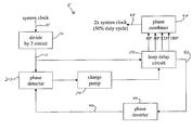
- FIG. 1 is a schematic block diagram of an apparatus to synthesize a clock signal in accordance with an embodiment of the present invention.
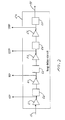
- FIG. 2 is a schematic block diagram of an analog loop delay circuit of the apparatus of FIG. 1 in accordance with an embodiment of the present invention.
- FIG. 3 is a schematic block diagram and associated timing diagram of a phase detector circuit of the apparatus of FIG. 1 in accordance with an embodiment of the present invention.
- FIG. 4 is a schematic block diagram and associated timing diagram of a phase combiner circuit of the apparatus of FIG. 1 in accordance with an embodiment of the present invention.
- FIG. 5 is a flowchart of a method to synthesize a clock signal using the apparatus of FIG. 1 in accordance with an embodiment of the present invention.
- FIG. 1 is a schematic block diagram of a clock synthesizer 5 that synthesizes a clock signal 65 in accordance with an embodiment of the present invention.
- the clock synthesizer 5 includes a divide-by-two circuit 10 , a phase detector 20 , a charge pump 30 , a phase inverter 40 , a loop delay circuit 50 , and a phase combiner 60 .
- the phase detector 20 , charge pump 30 , phase inverter 40 , and loop delay circuit 50 constitute a delay locked loop (DLL).
- DLL delay locked loop
- a system clock signal 15 is input to divide-by-two circuit 10 .
- An output of divide-by-two circuit 10 is connected to a first input of phase detector 20 and to a first input of loop delay circuit 50 .
- the output of phase detector 20 is connected to the input of charge pump 30 .
- the output of charge pump 30 is connected to a second input of loop delay circuit 50 .
- the outputs of loop delay circuit 50 are connected to inputs of phase combiner 60 .
- An output of loop delay circuit 50 is connected to the input of phase inverter 40 .
- the output of phase inverter 40 is connected to a second input of phase detector 20 .
- the output of phase combiner 60 is a synthesized clock signal 65 at twice the frequency of system clock 15 and having a 50% duty cycle.
- FIG. 5 is a flowchart of a method to synthesize a clock signal using the apparatus of FIG. 1 in accordance with an embodiment of the present invention.
- the frequency of system clock 15 is divided by a factor of two.
- the divide-by-two circuit 10 comprises a flip-flop that is clocked by the system clock 15 .
- the flip-flop output changes binary output states on the rising or falling edges of the system clock 15 , but not both.
- the output of the flip-flop is a half-clock signal 11 at half the frequency of the system clock signal 15 and having a duty cycle of 50%.
- the leading edge of the half-clock signal 11 is delayed in time from the leading edge of the system clock 15 by a time delay of TD 1 .
- the half-clock signal 11 is fed into phase detector 20 .
- a pulsed waveform is generated by phase detector 20 .
- the half-clock signal 11 is compared, in phase, to a feedback signal 42 that is generated in the step 140 .
- the feedback signal 42 is an output of the loop delay circuit 50 that is delayed by 180 degrees in phase with respect to the half-clock signal and then inverted.
- the phase inverter 40 comprises a flip-flop.
- the 180 -degree phase-delayed signal 41 is fed into an input of the flip-flop whose output goes low when the input goes high and vice-versa.
- the pulsewidth of the pulsed waveform is proportional to any phase difference, delta-phase, between the half-clock signal 11 and the feedback signal 42 .
- the phase detector 20 comprises an exclusive OR (XOR) gate as shown in FIG. 3. If signals A and B are inputs to the XOR gate, then the output is A XOR B as shown in FIG. 3. It may be seen that if signals A and B are exactly in phase with each other, the output of the phase detector 20 comprises a constant DC level of, for example, zero volts, indicating a phase-locked state.
- the pulsed waveform is fed to the input of charge pump 30 where a voltage level is generated in the step 120 .
- the voltage level is proportional to the pulsewidth of the pulsed waveform and, therefore, to the phase difference, delta-phase.
- the voltage level is fed to the loop delay circuit 50 and adjusts the phase delays of the phase-delayed signals that are generated in the step 130 .
- the loop delay circuit 50 comprises a set of analog delay elements 51 and a set of delay cancellers 52 as shown in FIG. 2.
- a set of four phase-delayed signals are generated by loop delay circuit 50 .
- the set of four phase-delayed signals are simply the half clock signal delayed in phase by approximately 45, 90, 135, and 180 degrees, respectively.
- the delays are kept locked at approximately 45, 90, 135, and 180 degrees by the feedback loop comprising phase detector 20 , charge pump 30 , loop delay circuit 50 , and phase inverter 40 .
- the set of delay cancellers 52 compensate for time delays and duty cycle distortion caused by the divide-by-two circuit 10 and the phase combiner 60 .
- Each delay canceller 52 adds a delay of (TD 1 +TD 2 ) where TD 1 is the time delay introduced by the divide-by-two circuit 10 and TD 2 is the time delay introduced by the phase combiner 60 .
- TD 1 is the time delay introduced by the divide-by-two circuit 10
- TD 2 is the time delay introduced by the phase combiner 60 .
- phase combiner 60 The set of phase-delayed signals are fed into phase combiner 60 where they are combined in the step 150 to generate a doubled clock signal 65 at twice the frequency of system clock signal 15 and having a duty cycle of 50%.
- the phase combiner is a combination of XOR circuits as shown in FIG. 4.
- the phase-delayed signals of approximately 45 degrees and 90 degrees are fed into XOR gate 61 and the phase-delayed signals of approximately 135 degrees and 180 degrees are fed into XOR gate 62 .
- the outputs of XOR gates 61 and 62 are fed into the inputs of XOR gate 63 .
- the output of XOR gate 63 is the doubled clock signal 65 as shown in FIG. 4.
- the doubled clock signal 65 may be used, for example, to double-clock an embedded memory on an ASIC chip.
- the doubled clock signal 65 may be applied to other applications as well.
- phase-delayed signals may be tapped off of the loop delay circuit 50 and used in other applications on the chip.
- the outputs of XOR gate 61 and/or XOR gate 62 may be tapped off of the phase combiner 60 and used in other applications on the chip.
- the clock synthesizer 5 may be implemented as a circuit of discrete components on, for example, a circuit board, instead of as embedded components on a chip, for applications in any of a plurality of possible discrete circuit layouts.
- phase detector 20 and charge pump 30 may be implemented as a single element instead of as two discrete elements connected in series.
- the design consumes a small area and 60% less power by using only 1 ⁇ 2 of the number of embedded delay elements on-chip (maximum phase delay of 180 degrees) as are needed in a classical full delay locked loop (DLL) design (maximum phase delay of 360 degrees). Furthermore, half clock signal locking error detection is much simpler than full clock locking.
- Another advantage of a present embodiment is the duty cycle rejection property. Full loop designs (360 degrees) have very limited tolerance to duty cycle variations in the incoming system clock 15 . An embodiment of the present invention may easily tolerate input system clock duty cycles of 5% to 95%.
- certain embodiments of the present invention afford an approach to achieve an efficient, low power, low chip area, embedded clock synthesis circuit.
- the circuit relies on dividing the frequency of a system clock by 2 and phase delaying the resultant half clock signal by a maximum of 180 degrees in a delay-locked loop design to generate a clock signal at twice the frequency of the system clock and having a 50% duty cycle.
Landscapes
- Physics & Mathematics (AREA)
- Nonlinear Science (AREA)
- Manipulation Of Pulses (AREA)
- Stabilization Of Oscillater, Synchronisation, Frequency Synthesizers (AREA)
Abstract
Description
- Certain embodiments of the present invention relate to the synthesis of a clock signal. More specifically, certain embodiments relate to a method and apparatus for efficiently synthesizing a clock signal on a chip such that the synthesized clock signal has a 50% duty cycle. The synthesized clock signal is derived from a system clock signal that is at half the frequency of the synthesized clock signal and whose duty cycle is not required to be 50%.
- Highly integrated System-on-Chip (SOC) implementations require clock synthesis and generation to be available on-chip. High speed and high-density memory designs require precise clocking elements to meet timing requirements. For example, one application is to double clock an embedded memory to make the embedded memory appear as a dual port. Double clocking may be accomplished, in part, by doubling the frequency of an existing system clock signal.
- Many embedded on-chip clock synthesis implementations consume significant amounts of power and chip area and also are dependent on the duty cycle of a system clock signal from which the synthesized clock signal is being derived. It is often desirable for a synthesized clock signal to have a 50% duty cycle, being independent of the clock signal from which the synthesized clock signal is derived. It is also desirable to synthesize a clock signal in an efficient manner to minimize power consumed and chip area consumed by the clock synthesizing circuitry.
- Further limitations and disadvantages of conventional and traditional approaches will become apparent to one of skill in the art, through comparison of such systems with embodiments of the present invention as set forth in the remainder of the present application with reference to the drawings.
- An embodiment of the present invention provides an efficient approach to synthesize a new clock signal from a current clock signal such that the new clock signal is at twice the frequency of the current clock signal. The new clock signal has a duty cycle of 50% that is not dependent on the duty cycle of the current clock signal.
- An efficient method is provided for doubling a first frequency of a first clock signal. The method includes generating a second clock signal at a second frequency by dividing the first frequency of the first clock signal by two, such that the second frequency is half of the first frequency and a duty cycle of the second clock signal is 50%. The method also includes generating a set of phase-delayed clock signals in response to the second clock signal such that the set of phase-delayed clock signals are delayed in phase with respect to the second clock signal. The method further includes combining the set of phase-delayed clock signals to generate a third clock signal at a third frequency, such that the third frequency is twice that of the first frequency and a duty cycle of the third clock signal is 50%.
- Apparatus is provided for doubling a first frequency of a first clock signal. The apparatus includes a divide-by-two circuit that generates a second clock signal at a second frequency that is half of the first frequency, such that a duty cycle of the second clock signal is 50%. The apparatus also includes a delay locked loop (DLL) circuit responsive to the second clock signal to generate a set of phase-delayed clock signals that are delayed in phase with respect to the second clock signal. Further, the apparatus includes a phase combiner circuit responsive to the set of phase-delayed clock signals to generate a third clock signal at a third frequency, such that the third frequency is twice that of the first frequency and a duty cycle of said third clock signal is 50%.
- Certain embodiments of the present invention afford an efficient approach for synthesizing a new clock signal from a current clock signal by doubling the frequency of the current clock signal and establishing a 50% duty cycle for the new clock signal that is not dependent on the duty cycle of the current clock signal.
- FIG. 1 is a schematic block diagram of an apparatus to synthesize a clock signal in accordance with an embodiment of the present invention.
- FIG. 2 is a schematic block diagram of an analog loop delay circuit of the apparatus of FIG. 1 in accordance with an embodiment of the present invention.
- FIG. 3 is a schematic block diagram and associated timing diagram of a phase detector circuit of the apparatus of FIG. 1 in accordance with an embodiment of the present invention.
- FIG. 4 is a schematic block diagram and associated timing diagram of a phase combiner circuit of the apparatus of FIG. 1 in accordance with an embodiment of the present invention.
- FIG. 5 is a flowchart of a method to synthesize a clock signal using the apparatus of FIG. 1 in accordance with an embodiment of the present invention.
- FIG. 1 is a schematic block diagram of a
clock synthesizer 5 that synthesizes aclock signal 65 in accordance with an embodiment of the present invention. Theclock synthesizer 5 includes a divide-by-two circuit 10, a phase detector 20, acharge pump 30, aphase inverter 40, aloop delay circuit 50, and a phase combiner 60. The phase detector 20,charge pump 30,phase inverter 40, andloop delay circuit 50 constitute a delay locked loop (DLL). - Referring to FIG. 1, in an embodiment of the present invention, a
system clock signal 15 is input to divide-by-two circuit 10. An output of divide-by-two circuit 10 is connected to a first input of phase detector 20 and to a first input ofloop delay circuit 50. The output of phase detector 20 is connected to the input ofcharge pump 30. The output ofcharge pump 30 is connected to a second input ofloop delay circuit 50. The outputs ofloop delay circuit 50 are connected to inputs of phase combiner 60. An output ofloop delay circuit 50 is connected to the input ofphase inverter 40. The output ofphase inverter 40 is connected to a second input of phase detector 20. The output of phase combiner 60 is a synthesizedclock signal 65 at twice the frequency ofsystem clock 15 and having a 50% duty cycle. - FIG. 5 is a flowchart of a method to synthesize a clock signal using the apparatus of FIG. 1 in accordance with an embodiment of the present invention. In the
step 100, the frequency ofsystem clock 15 is divided by a factor of two. In an embodiment of the present invention, the divide-by-two circuit 10 comprises a flip-flop that is clocked by thesystem clock 15. The flip-flop output changes binary output states on the rising or falling edges of thesystem clock 15, but not both. As a result, the output of the flip-flop is a half-clock signal 11 at half the frequency of thesystem clock signal 15 and having a duty cycle of 50%. However, the leading edge of the half-clock signal 11 is delayed in time from the leading edge of thesystem clock 15 by a time delay of TD1. - The half-clock signal 11 is fed into phase detector 20. In the step 110 of FIG. 5, a pulsed waveform is generated by phase detector 20. The half-clock signal 11 is compared, in phase, to a
feedback signal 42 that is generated in thestep 140. In an embodiment of the present invention, thefeedback signal 42 is an output of theloop delay circuit 50 that is delayed by 180 degrees in phase with respect to the half-clock signal and then inverted. Thephase inverter 40 comprises a flip-flop. The 180-degree phase-delayed signal 41 is fed into an input of the flip-flop whose output goes low when the input goes high and vice-versa. - The pulsewidth of the pulsed waveform is proportional to any phase difference, delta-phase, between the half-clock signal 11 and the
feedback signal 42. In an embodiment of the present invention, the phase detector 20 comprises an exclusive OR (XOR) gate as shown in FIG. 3. If signals A and B are inputs to the XOR gate, then the output is A XOR B as shown in FIG. 3. It may be seen that if signals A and B are exactly in phase with each other, the output of the phase detector 20 comprises a constant DC level of, for example, zero volts, indicating a phase-locked state. - The pulsed waveform is fed to the input of
charge pump 30 where a voltage level is generated in the step 120. The voltage level is proportional to the pulsewidth of the pulsed waveform and, therefore, to the phase difference, delta-phase. - The voltage level is fed to the
loop delay circuit 50 and adjusts the phase delays of the phase-delayed signals that are generated in the step 130. Theloop delay circuit 50 comprises a set of analog delay elements 51 and a set ofdelay cancellers 52 as shown in FIG. 2. In step 130, a set of four phase-delayed signals are generated byloop delay circuit 50. The set of four phase-delayed signals are simply the half clock signal delayed in phase by approximately 45, 90, 135, and 180 degrees, respectively. The delays are kept locked at approximately 45, 90, 135, and 180 degrees by the feedback loop comprising phase detector 20,charge pump 30,loop delay circuit 50, andphase inverter 40. The set ofdelay cancellers 52 compensate for time delays and duty cycle distortion caused by the divide-by-two circuit 10 and thephase combiner 60. Eachdelay canceller 52 adds a delay of (TD1+TD2) where TD1 is the time delay introduced by the divide-by-two circuit 10 and TD2 is the time delay introduced by thephase combiner 60. As a result, the leading edge of the 2×system clock 65 stays lined up with the leading edge of thesystem clock 15 and the duty cycle of the 2×system clock 65 remains at 50%. - The set of phase-delayed signals are fed into
phase combiner 60 where they are combined in the step 150 to generate a doubledclock signal 65 at twice the frequency ofsystem clock signal 15 and having a duty cycle of 50%. - In an embodiment of the present invention, the phase combiner is a combination of XOR circuits as shown in FIG. 4. The phase-delayed signals of approximately 45 degrees and 90 degrees are fed into XOR gate 61 and the phase-delayed signals of approximately 135 degrees and 180 degrees are fed into
XOR gate 62. The outputs ofXOR gates 61 and 62 are fed into the inputs ofXOR gate 63. The output ofXOR gate 63 is the doubledclock signal 65 as shown in FIG. 4. The doubledclock signal 65 may be used, for example, to double-clock an embedded memory on an ASIC chip. The doubledclock signal 65 may be applied to other applications as well. - As one possible alternative, the phase-delayed signals may be tapped off of the
loop delay circuit 50 and used in other applications on the chip. Also, the outputs of XOR gate 61 and/orXOR gate 62 may be tapped off of thephase combiner 60 and used in other applications on the chip. - As a further alternative, the
clock synthesizer 5 may be implemented as a circuit of discrete components on, for example, a circuit board, instead of as embedded components on a chip, for applications in any of a plurality of possible discrete circuit layouts. - The various elements of the
clock synthesizer 5 may be combined or separated according to various embodiments of the present invention. For example, the phase detector 20 andcharge pump 30 may be implemented as a single element instead of as two discrete elements connected in series. - In an embodiment of the present invention, the design consumes a small area and 60% less power by using only ½ of the number of embedded delay elements on-chip (maximum phase delay of 180 degrees) as are needed in a classical full delay locked loop (DLL) design (maximum phase delay of 360 degrees). Furthermore, half clock signal locking error detection is much simpler than full clock locking. Another advantage of a present embodiment is the duty cycle rejection property. Full loop designs (360 degrees) have very limited tolerance to duty cycle variations in the
incoming system clock 15. An embodiment of the present invention may easily tolerate input system clock duty cycles of 5% to 95%. - In summary, certain embodiments of the present invention afford an approach to achieve an efficient, low power, low chip area, embedded clock synthesis circuit. The circuit relies on dividing the frequency of a system clock by 2 and phase delaying the resultant half clock signal by a maximum of 180 degrees in a delay-locked loop design to generate a clock signal at twice the frequency of the system clock and having a 50% duty cycle.
- While the invention has been described with reference to certain embodiments, it will be understood by those skilled in the art that various changes may be made and equivalents may be substituted without departing from the scope of the invention. In addition, many modifications may be made to adapt a particular situation or material to the teachings of the invention without departing from its scope. Therefore, it is intended that the invention not be limited to the particular embodiment disclosed, but that the invention will include all embodiments falling within the scope of the appended claims.
Claims (26)
Priority Applications (2)
| Application Number | Priority Date | Filing Date | Title |
|---|---|---|---|
| US10/128,325 US6653876B2 (en) | 2002-04-23 | 2002-04-23 | Method and apparatus for synthesizing a clock signal using a compact and low power delay locked loop (DLL) |
| US10/654,711 US7002383B1 (en) | 2002-04-23 | 2003-09-04 | Method and apparatus for synthesizing a clock signal using a compact and low power delay locked loop (DLL) |
Applications Claiming Priority (1)
| Application Number | Priority Date | Filing Date | Title |
|---|---|---|---|
| US10/128,325 US6653876B2 (en) | 2002-04-23 | 2002-04-23 | Method and apparatus for synthesizing a clock signal using a compact and low power delay locked loop (DLL) |
Related Child Applications (1)
| Application Number | Title | Priority Date | Filing Date |
|---|---|---|---|
| US10/654,711 Continuation US7002383B1 (en) | 2002-04-23 | 2003-09-04 | Method and apparatus for synthesizing a clock signal using a compact and low power delay locked loop (DLL) |
Publications (2)
| Publication Number | Publication Date |
|---|---|
| US20030197536A1 true US20030197536A1 (en) | 2003-10-23 |
| US6653876B2 US6653876B2 (en) | 2003-11-25 |
Family
ID=29215442
Family Applications (2)
| Application Number | Title | Priority Date | Filing Date |
|---|---|---|---|
| US10/128,325 Expired - Lifetime US6653876B2 (en) | 2002-04-23 | 2002-04-23 | Method and apparatus for synthesizing a clock signal using a compact and low power delay locked loop (DLL) |
| US10/654,711 Expired - Lifetime US7002383B1 (en) | 2002-04-23 | 2003-09-04 | Method and apparatus for synthesizing a clock signal using a compact and low power delay locked loop (DLL) |
Family Applications After (1)
| Application Number | Title | Priority Date | Filing Date |
|---|---|---|---|
| US10/654,711 Expired - Lifetime US7002383B1 (en) | 2002-04-23 | 2003-09-04 | Method and apparatus for synthesizing a clock signal using a compact and low power delay locked loop (DLL) |
Country Status (1)
| Country | Link |
|---|---|
| US (2) | US6653876B2 (en) |
Cited By (3)
| Publication number | Priority date | Publication date | Assignee | Title |
|---|---|---|---|---|
| US20070286321A1 (en) * | 2006-06-13 | 2007-12-13 | Gupta Atul K | Linear sample and hold phase detector for clocking circuits |
| US10644710B2 (en) * | 2018-08-21 | 2020-05-05 | Electronics And Telecommunications Research Institute | Electronic circuit for adjusting phase of clock |
| US20240340013A1 (en) * | 2023-04-06 | 2024-10-10 | Winbond Electronics Corp. | Delay locked loop |
Families Citing this family (10)
| Publication number | Priority date | Publication date | Assignee | Title |
|---|---|---|---|---|
| US6870415B2 (en) * | 2002-09-12 | 2005-03-22 | Broadcom Corporation | Delay generator with controlled delay circuit |
| US7123063B2 (en) * | 2004-04-28 | 2006-10-17 | Broadcom Corporation | Supply tracking clock multiplier |
| US7675336B1 (en) * | 2004-12-17 | 2010-03-09 | Altera Corporation | Clock duty cycle recovery circuit |
| US7116143B2 (en) * | 2004-12-30 | 2006-10-03 | Micron Technology, Inc. | Synchronous clock generator including duty cycle correction |
| US7158443B2 (en) * | 2005-06-01 | 2007-01-02 | Micron Technology, Inc. | Delay-lock loop and method adapting itself to operate over a wide frequency range |
| KR100701704B1 (en) * | 2006-01-12 | 2007-03-29 | 주식회사 하이닉스반도체 | Duty cycle correction circuit |
| KR20090107256A (en) * | 2008-04-08 | 2009-10-13 | 삼성전자주식회사 | Duty cycle correction circuit |
| US9590638B2 (en) | 2012-09-07 | 2017-03-07 | University Of Virginia Patent Foundation | Low power clock source |
| US9954517B2 (en) | 2012-11-06 | 2018-04-24 | Micron Technology, Inc. | Apparatuses and methods for duty cycle adjustment |
| US9413338B2 (en) | 2014-05-22 | 2016-08-09 | Micron Technology, Inc. | Apparatuses, methods, and circuits including a duty cycle adjustment circuit |
Family Cites Families (10)
| Publication number | Priority date | Publication date | Assignee | Title |
|---|---|---|---|---|
| US3993957A (en) * | 1976-03-08 | 1976-11-23 | International Business Machines Corporation | Clock converter circuit |
| US6150855A (en) * | 1990-02-06 | 2000-11-21 | Bull, S.A. | Phase-locked loop and resulting frequency multiplier |
| FR2658015B1 (en) * | 1990-02-06 | 1994-07-29 | Bull Sa | LOCKED PHASE CIRCUIT AND RESULTING FREQUENCY MULTIPLIER. |
| SE515076C2 (en) * | 1992-07-01 | 2001-06-05 | Ericsson Telefon Ab L M | Multiplexer / demultiplexer circuit |
| JPH07202649A (en) * | 1993-12-27 | 1995-08-04 | Toshiba Corp | Multiplier circuit |
| US5537068A (en) * | 1994-09-06 | 1996-07-16 | Intel Corporation | Differential delay line clock generator |
| JP3323054B2 (en) * | 1996-04-01 | 2002-09-09 | 株式会社東芝 | Frequency multiplier |
| KR100214559B1 (en) * | 1997-02-20 | 1999-08-02 | 구본준 | Frequency doubling |
| KR100319607B1 (en) * | 1999-02-25 | 2002-01-09 | 김영환 | Analog dll circuit |
| CA2270516C (en) * | 1999-04-30 | 2009-11-17 | Mosaid Technologies Incorporated | Frequency-doubling delay locked loop |
-
2002
- 2002-04-23 US US10/128,325 patent/US6653876B2/en not_active Expired - Lifetime
-
2003
- 2003-09-04 US US10/654,711 patent/US7002383B1/en not_active Expired - Lifetime
Cited By (5)
| Publication number | Priority date | Publication date | Assignee | Title |
|---|---|---|---|---|
| US20070286321A1 (en) * | 2006-06-13 | 2007-12-13 | Gupta Atul K | Linear sample and hold phase detector for clocking circuits |
| US7764759B2 (en) * | 2006-06-13 | 2010-07-27 | Gennum Corporation | Linear sample and hold phase detector for clocking circuits |
| US10644710B2 (en) * | 2018-08-21 | 2020-05-05 | Electronics And Telecommunications Research Institute | Electronic circuit for adjusting phase of clock |
| US20240340013A1 (en) * | 2023-04-06 | 2024-10-10 | Winbond Electronics Corp. | Delay locked loop |
| US12289113B2 (en) * | 2023-04-06 | 2025-04-29 | Windbond Electronics Corp. | Delay locked loop |
Also Published As
| Publication number | Publication date |
|---|---|
| US6653876B2 (en) | 2003-11-25 |
| US7002383B1 (en) | 2006-02-21 |
Similar Documents
| Publication | Publication Date | Title |
|---|---|---|
| JP4677511B2 (en) | Frequency multiplication delay lock loop | |
| CN100505545C (en) | Duty cycle correction circuit and delay locked loop with the circuit | |
| EP0753808B1 (en) | Clock distributing circuit | |
| KR100269316B1 (en) | Delayed locked loop & phase locked loop merged with synchronous delay circuit | |
| US6784707B2 (en) | Delay locked loop clock generator | |
| KR100319607B1 (en) | Analog dll circuit | |
| US5517147A (en) | Multiple-phase clock signal generator for integrated circuits, comprising PLL, counter, and logic circuits | |
| Shin et al. | A 7 ps jitter 0.053 mm $^{2} $ fast lock all-digital DLL with a wide range and high resolution DCC | |
| US6653876B2 (en) | Method and apparatus for synthesizing a clock signal using a compact and low power delay locked loop (DLL) | |
| KR20030039994A (en) | Apparatus for ensuring the correct start-up and locking of a delay locked loop | |
| US5818270A (en) | Temperature independent, wide range frequency clock multiplier | |
| US7061287B2 (en) | Delay locked loop | |
| JP3779713B2 (en) | Semiconductor integrated circuit | |
| US6967536B2 (en) | Phase-locked loop circuit reducing steady state phase error | |
| US7199624B2 (en) | Phase locked loop system capable of deskewing | |
| US6477657B1 (en) | Circuit for I/O clock generation | |
| KR100541684B1 (en) | Delay Locked Loop Device | |
| US6977539B1 (en) | Clock signal generators having programmable full-period clock skew control and methods of generating clock signals having programmable skews | |
| KR19990042341A (en) | Delay Synchronous Loop (DL) Combined with Clock Synchronous Delay Circuit | |
| US7519087B2 (en) | Frequency multiply circuit using SMD, with arbitrary multiplication factor | |
| JP3786540B2 (en) | Timing control circuit device | |
| Gandage et al. | Design and Implementation of Low Power Delay Locked Loop using Multiplexer Based Phase Frequency Detector | |
| Moon et al. | A 62.5-250 mhz multi-phase delay-locked loop using a replica delay line with triply controlled delay cells | |
| Liran et al. | All-digital dll architecture and applications | |
| JP2776328B2 (en) | PLL circuit |
Legal Events
| Date | Code | Title | Description |
|---|---|---|---|
| AS | Assignment |
Owner name: BROADCOM CORPORATION, CALIFORNIA Free format text: ASSIGNMENT OF ASSIGNORS INTEREST;ASSIGNORS:ISSA, SAMI;AFGHAHI, MORTEZA (CYRUS);REEL/FRAME:013099/0180 Effective date: 20020412 |
|
| STCF | Information on status: patent grant |
Free format text: PATENTED CASE |
|
| FPAY | Fee payment |
Year of fee payment: 4 |
|
| FPAY | Fee payment |
Year of fee payment: 8 |
|
| FPAY | Fee payment |
Year of fee payment: 12 |
|
| AS | Assignment |
Owner name: BANK OF AMERICA, N.A., AS COLLATERAL AGENT, NORTH CAROLINA Free format text: PATENT SECURITY AGREEMENT;ASSIGNOR:BROADCOM CORPORATION;REEL/FRAME:037806/0001 Effective date: 20160201 Owner name: BANK OF AMERICA, N.A., AS COLLATERAL AGENT, NORTH Free format text: PATENT SECURITY AGREEMENT;ASSIGNOR:BROADCOM CORPORATION;REEL/FRAME:037806/0001 Effective date: 20160201 |
|
| AS | Assignment |
Owner name: AVAGO TECHNOLOGIES GENERAL IP (SINGAPORE) PTE. LTD., SINGAPORE Free format text: ASSIGNMENT OF ASSIGNORS INTEREST;ASSIGNOR:BROADCOM CORPORATION;REEL/FRAME:041706/0001 Effective date: 20170120 Owner name: AVAGO TECHNOLOGIES GENERAL IP (SINGAPORE) PTE. LTD Free format text: ASSIGNMENT OF ASSIGNORS INTEREST;ASSIGNOR:BROADCOM CORPORATION;REEL/FRAME:041706/0001 Effective date: 20170120 |
|
| AS | Assignment |
Owner name: BROADCOM CORPORATION, CALIFORNIA Free format text: TERMINATION AND RELEASE OF SECURITY INTEREST IN PATENTS;ASSIGNOR:BANK OF AMERICA, N.A., AS COLLATERAL AGENT;REEL/FRAME:041712/0001 Effective date: 20170119 |
|
| AS | Assignment |
Owner name: AVAGO TECHNOLOGIES INTERNATIONAL SALES PTE. LIMITED, SINGAPORE Free format text: MERGER;ASSIGNOR:AVAGO TECHNOLOGIES GENERAL IP (SINGAPORE) PTE. LTD.;REEL/FRAME:047195/0026 Effective date: 20180509 Owner name: AVAGO TECHNOLOGIES INTERNATIONAL SALES PTE. LIMITE Free format text: MERGER;ASSIGNOR:AVAGO TECHNOLOGIES GENERAL IP (SINGAPORE) PTE. LTD.;REEL/FRAME:047195/0026 Effective date: 20180509 |
|
| AS | Assignment |
Owner name: AVAGO TECHNOLOGIES INTERNATIONAL SALES PTE. LIMITED, SINGAPORE Free format text: CORRECTIVE ASSIGNMENT TO CORRECT THE EFFECTIVE DATE OF MERGER PREVIOUSLY RECORDED ON REEL 047195 FRAME 0026. ASSIGNOR(S) HEREBY CONFIRMS THE MERGER;ASSIGNOR:AVAGO TECHNOLOGIES GENERAL IP (SINGAPORE) PTE. LTD.;REEL/FRAME:047477/0423 Effective date: 20180905 Owner name: AVAGO TECHNOLOGIES INTERNATIONAL SALES PTE. LIMITE Free format text: CORRECTIVE ASSIGNMENT TO CORRECT THE EFFECTIVE DATE OF MERGER PREVIOUSLY RECORDED ON REEL 047195 FRAME 0026. ASSIGNOR(S) HEREBY CONFIRMS THE MERGER;ASSIGNOR:AVAGO TECHNOLOGIES GENERAL IP (SINGAPORE) PTE. LTD.;REEL/FRAME:047477/0423 Effective date: 20180905 |