JP3786540B2 - Timing control circuit device - Google Patents
Timing control circuit device Download PDFInfo
- Publication number
- JP3786540B2 JP3786540B2 JP10754299A JP10754299A JP3786540B2 JP 3786540 B2 JP3786540 B2 JP 3786540B2 JP 10754299 A JP10754299 A JP 10754299A JP 10754299 A JP10754299 A JP 10754299A JP 3786540 B2 JP3786540 B2 JP 3786540B2
- Authority
- JP
- Japan
- Prior art keywords
- circuit
- delay
- transmission signal
- signal
- timing control
- Prior art date
- Legal status (The legal status is an assumption and is not a legal conclusion. Google has not performed a legal analysis and makes no representation as to the accuracy of the status listed.)
- Expired - Fee Related
Links
Images


Classifications
-
- Y02B60/31—
Description
【0001】
【発明の属する技術分野】
本発明は、半導体集積回路に係わり、特に同期信号の発生、伝達または分配を行うタイミング制御回路に関する。
【0002】
【従来の技術】
半導体集積回路装置において、クロックを生成する装置として主に、位相同期ループ(PLL)、ディレー・ロックド・ループ(DLL)が用いられている。1995インターナショナル・ソリッド・ステート・サーキッツ・コンファレンス・ダイジェスト・オブ・テクニカル・ペーパーズ(1995年)第112頁から第113頁(1995 International Solid-State Circuits Conference、 Digest of Technical Papers、 pp.112-113)に述べられているようにPLLは、クロック信号が同期して安定した信号出力を発生するまでにかかるセットリング時間に長時間(数10μ秒程度)を必要とする。同様に、1998インターナショナル・ソリッド・ステート・サーキッツ・コンファレンス・ダイジェスト・オブ・テクニカル・ペーパーズ(1998年)第158頁から第159頁(1998 International Solid-State Circuits Conference、 Digest of Technical Papers、 pp.158-159)で述べられているように、DLLではセットリング時間(ロッキング時間)がクロック100周期程度と長い。通常、半導体集積回路装置を用いたシステムがスタンドバイ状態になる時、PLLあるいはDLLを停止し、PLL、DLLで消費する電力を削減する。しかし、前述したようにPLLやDLLをスタンドバイ状態から動作状態へ復帰させるには、長いセットリング時間を必要とする。このためシステムによっては、この長いセットリング時間を避けるために、待機時でもPLLあるいはDLLを停止させないようなスリープモードを設けているものもある。このスリープモードでは、PLLあるいはDLLで電力を消費してしまう。
【0003】
以上のPLL、DLLに特有の欠点を解決する方法として、1997シンポジウム・オン・ヴィエルエスアイ・サーキッツ・ダイジェスト・オブ・テクニカル・ペーパーズ(1997年)第109頁から第110頁(1997 Symposium on VLSI Circuits、 Digest of Technical Papers、 pp.109-110)では、シンクロナス・ミラー・ディレー(SMD)が提案されている。SMDは、セットリング時間がクロック2周期と短い。SMDでは、出力の負荷を模擬したダミー遅延回路を用意し、これを用いてクロック信号を同期させる。そのため、出力の負荷が未知である場合や、変化する場合には、対応できない。このSMDの欠点を解決する策として、プロシーディングス・オブ・ザ・1998・カスタム・インテグレーティッド・サーキッツ・コンファレンス(1998年)第511頁から第514頁(Proceedings of the 1998 Custom Integrated Circuits Conference、 pp.511-514)においてダイレクトSMD(D-SMD)が提案された。しかしながら、どちらのSMDにおいても、出力クロック信号のデューティ比が1/10程度という極端な信号しか得られず、クロック信号の立ち上がりと立ち下がりの両方を利用するシステムにおいては、使用することができない。
【0004】
【発明が解決しようとする課題】
出願人らは、特願平10-250728において、以上のPLL、DLL、SMD、D-SMDに存在する欠点をすべて克服するタイミング制御回路装置を開発した。この装置では、セットリング時間がクロック信号2〜3周期と短く、出力負荷の変化に関わらずクロック信号の同期をとることができ、また出力クロック信号のデューティ比を1/1にそろえることができる。
【0005】
図3または図4は、出願人らが特願平10-250728で提案したタイミング制御回路装置の構成を示している。入力クロック信号clkin31はバッファ回路BUF31、遅延制御回路列DCL31を経由して遅延クロック信号dclk31として出力され、クロックドライバDRV31や容量性負荷LD31を経て出力クロック信号clkout31となりシステム等にクロック信号を供給する。入力クロック信号clkin31の周期をTin、クロックドライバDRV31の遅延時間をTdrvとすると、フォワード遅延回路列FDA31及び制御回路MCC31及び制御信号記憶回路REG31は遅延クロック信号dclk31と出力クロック信号clkout31の位相差を検出して、Tfda=Tin−Tdrvとなるフォワード遅延回路列FDA31内の遅延素子位置を決定する。この位置は、遅延制御回路列DCL31に伝えられ、DCL31内で遅延時間がTdcl=Tfda=Tin−Tdrvとなる位置が選択される。すると、入力クロック信号clkin31から出力クロック信号clkout31までの遅延時間はTout=Tdcl+Tdrv=Tinとなり、入力に対してちょうど1周期遅れたクロック信号が出力される事になる。
【0006】
このようにして、クロック信号の同期をとるタイミング制御回路では、セットリングタイムが2〜3周期と短く、また出力の負荷(ここではDRV31やLD31)が変化しても同期信号を生成でき、またデューティ比に関しては、入力クロック信号のデューティ比をそのまま伝える事ができる。あるいは、遅延素子DEL31を調整する事により任意のデューティ比を持った信号を出力できる。さて、このタイミング制御回路装置の動作可能な最低クロック周波数は、Fmin=1 /(n×Tdel)で与える事ができる。また、この装置の発生するクロック信号が示す入力信号とのスキューの最大値は、Smax=Tdelとなる。ここで、nは遅延制御回路列DCL31内にある遅延素子DEL31の段数、Tdelは1段あたりの遅延素子DEL31が有する遅延時間である。これらの関係からわかる通り、このタイミング制御回路装置では、動作最低周波数Fminを変えずにスキューSmaxを小さくするためには1段の遅延素子あたりの遅延時間Tdelを小さくする必要があり、その場合遅延素子の段数nが増加してしまう。逆に、動作最低周波数Fminを変えずに遅延素子の段数nを減らそうとするとスキューSmaxが大きくなってしまう。回路の面積や消費電力は遅延素子の段数nに依存するので、装置の性能を表すスキューと、面積・消費電力がトレードオフの関係になる。
【0007】
本発明の課題は、上記の特願平10-250728で提案したタイミング制御回路装置をさらに優れたものとし、低スキューでかつ面積・消費電力の少ないタイミング制御回路装置を提供する事にある。
【0008】
すなわち、タイミング制御回路装置において、セットリング時間が短く、クロックバッファ等の負荷が変化しても同期が可能であり、出力クロック信号のデューティ比を調節でき、さらに、出力クロック信号のスキューと面積・消費電力を同時に低減することのできるタイミング制御回路装置を提供する事にある。
【0009】
【課題を解決するための手段】
上記課題を解決するため、タイミング制御回路装置には基準クロック信号が入力され、これを用いて内部クロック信号を生成し、さらにクロックドライバ回路等の負荷回路を経由して出力クロック信号を生成する。この時、タイミング制御回路装置には出力クロック信号を帰還して入力し、出力クロック信号と基準クロック信号が同相になるように内部クロック信号を生成する。
【0010】
また、タイミング制御回路内装置には、内部クロックと出力クロックの位相差を検出する回路と遅延量が制御可能な遅延回路があり、遅延回路は前記検出された位相差により遅延量を変えられるようになっている。その結果、出力クロック信号と基準クロック信号を同相にできる。
【0011】
タイミング制御回路装置は粗調タイミング制御回路と微調タイミング制御回路から構成され、粗調タイミング制御回路で低い精度で出力クロック信号と基準クロック信号の位相を同期させ、微調タイミング制御回路では高い精度で出力クロック信号と基準クロック信号の位相を同期させる。生成される出力クロック信号のスキューは、微調タイミング制御回路内の遅延素子で決定され、遅延素子1段あたりの遅延量を小さくする事でスキューを小さくできる。タイミング制御回路の回路規模は粗調タイミング制御回路内の遅延素子と微調タイミング制御回路内の遅延素子の遅延量の比によって任意に増減でき、最適な比を用いる事で回路規模、面積、消費電力を削減できる。
【0012】
本発明の実施例によると、クロック信号出力が安定するセットリング時間が短く、その結果半導体回路装置内で必要な時にのみ動作させることにより低電力化が可能となり、また電源電圧の低下等による出力信号の制御精度劣化を抑制でき、また、クロック出力の負荷回路における負荷変化に対応できるという、特願平10-250728のタイミング制御回路装置の特性を持ち、さらに、低スキュー、低面積、低消費電力を同時に実現できるタイミング制御回路装置を提供できる。
【0013】
【発明の実施の形態】
以下、図を参照して本発明の実施例を説明する。
【0014】
図2は、本発明の実施例を示す図である。
【0015】
以下の説明では、バッファ回路、オフセット回路、n入力NOR回路、分周回路が持つ遅延時間は、他の構成要素が持つ遅延時間と比べて小さい事と、説明の都合上、無視できるものと仮定して説明する。
【0016】
入力クロック信号clkin21は粗調タイミング制御回路CDLL21に入力され、遅延クロック信号dclk23と制御信号cntsig21、cntsig22を生成する。粗調微調変換回路CONV21は粗調タイミング制御回路CDLL21から出力される制御信号cntsig21、cntsig22を受け取り、微調タイミング制御回路のための遅延クロック信号dclk22を生成して伝える。微調タイミング制御回路FDLL21は、遅延クロック信号dclk22とdclk23を受け取り、遅延クロック信号dclk21を新たに生成して出力する。クロックドライバDRV21は遅延クロック信号dclk21を受け、出力クロック信号clkout21として容量性負荷LD21へクロック信号を分配する。出力クロック信号clkout21は再び粗調タイミング制御回路CDLL21に帰還する。粗調タイミング制御回路CDLL21は、遅延制御回路列DCL22、フォワード遅延回路列FDA22、制御回路MCC22、制御信号記憶回路REG22と、さらにバッファ回路BUF21、BUF24、BUF25、n入力NOR回路NNOR22、分周回路DIV22、オフセット調整回路offset21で構成されている。クロックドライバの遅延時間をTdrvとすると、遅延クロック信号dclk21と出力クロック信号clkout21の信号間の遅延時間はTdrvとなる。粗調タイミング制御回路CDLL21では、出力クロック信号clkout21をオフセット回路offsett21が受けた後にフォワード遅延回路列FDA22に入力し、遅延クロック信号dclk21をバッファ回路BUF25が受けた後に制御回路MCC22に入力する。入力クロック信号clkin21のクロック周期をTinとする時、制御回路MCC22はフォワード遅延回路列FDA22の遅延クロック信号が、遅延時間Tfda=Tin−Tdrvとなる位置を検出する。制御信号記憶回路REG22は、制御回路MCC22が検出した位置を記憶する。
【0017】
記憶を行うタイミングは、分周回路DIV22によって遅延クロック信号dclk21が分周されたタイミングによる。分周回路DIV22は内部クロック信号inclk22を生成し、バッファ回路BUF24を経て制御信号記憶回路REG22へ信号を与え、制御回路MCC22の検出位置を記憶させる。この記憶された制御信号cntsig22は遅延制御回路列DCL22の遅延伝達位置を決定し、バッファ回路BUF21を経て入力される入力クロック信号clkin21をTdcl=Tfda=Tin−Tdrvの遅延時間だけ送らせて遅延信号dclk23として出力する。この遅延信号dclk23が、微調タイミング制御回路FDLL21内の遅延制御回路列DCL21を遅延を持たずに素通りすると、出力クロック信号clkout21の遅延時間は、Tout=Tdcl+Tdrv=Tinとなり、ちょうど入力クロック信号clkin21と1周期遅れた信号が伝わる事になり、入力信号と出力信号の位相が同期する。n入力NOR回路NNOR22によって、回路起動時などで、遅延位置がどこも選択されなかった場合に、遅延制御回路列を経由しないで入力クロック信号clkin21を遅延クロック信号dclk23として伝える事ができる。また、オフセット回路offset21はタイミング制御回路装置内部に存在する自己遅延を保証するための遅延素子である。
【0018】
しかし、実際に遅延制御回路列DCL22で選ばれる遅延時間は不連続なディジタル量であり、遅延制御回路列DCL22を構成する遅延素子1段あたりの遅延時間が、入出力信号間の位相誤差(スキュー)として残る。そこで、この位相誤差分を微調タイミング制御回路FDLL21で調整する。粗調微調変換回路CONV21はフォワード遅延回路列FDA22で選択された位置まで伝達した遅延クロック信号を制御信号cntsig21として受け取り、微調タイミング制御回路FDLL21内のフォワード遅延回路列FDA21へ遅延クロック信号dclk22として伝える。
【0019】
また、入力クロック信号clkin21が遅延制御回路列DCL22によって粗調整された遅延信号dclk23も同様に、微調タイミング制御回路FDLL21内の遅延制御回路列DCL21に伝達される。微調タイミング制御回路FDLL21内では粗調タイミング制御回路CDLL21と同様のタイミング制御が行われ、微調整された遅延信号dclk21を出力する。以上の操作により、入力クロック信号clkin21と出力クロック信号clkout21は、微調タイミング制御回路FDLL21内の遅延制御回路列DCL21を構成する遅延素子1段の持つ遅延時間以内で同期をとることができる。
【0020】
例えば、入力クロック信号の周期が10ns(周波数100MHz)とする。微調タイミング制御回路CDLL21内の遅延制御回路列DCL22を構成する遅延素子1段の遅延時間が1nsだとすると、この入力クロック信号に対して負荷回路やクロックドライバによらずに同期を取るためには、10段の遅延素子が必要となり、この時の最大スキューSmax=1nsとなる。微調タイミング制御回路FDLL21では、遅延制御回路列DCL21を構成する遅延素子1段の遅延時間を100psだとすると、やはり10段の遅延素子が必要となり、最大スキューSmax=100psとなる。遅延素子の段数は、合計20段で構成できる。これに対して、特願平10-250728のタイミング制御回路装置で10nsの入力クロック信号を同期させようとした場合、遅延素子の段数を20段で構成しようとすると、最大スキューSmax=500psと増加する。あるいは、最大スキューSmax=100psを実現しようとすると、遅延素子の段数が100段必要となり、回路規模、面積や消費電力が増大する事になる。従って、本実施例にある回路を用いると、特願平10-250728のタイミング制御回路装置と同じ特徴を維持しながら、さらにスキュー低減と回路規模、面積、消費電力の削減を同時に行う事ができる。
【0021】
図1は本発明の詳細な実施例を示す図である。
【0022】
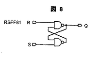
フォワード遅延回路列FDA11、12は、AND回路で形成することができる。制御回路MCC11、12はRS型フリップフロップ回路RSFF11とインバータ回路、NOR回路で構成される。制御信号記憶回路REG11、12はD型フリップフロップ回路DFF11で構成される。遅延制御回路列DCL11、12はAND回路とNAND回路で構成される。また、粗調微調変換回路CONV11はMOSトランジスタを用いたスイッチで構成することができる。また、図5にバッファ回路BUF11、12、13、14、15の実施例を、図6にn入力NOR回路NNOR11、12の実施例を、図7にD型フリップフロップ回路DFF11の実施例を、図8にRS型フリップフロップ回路RSFF11の実施例を、図9に分周回路DIV11、12の実施例を、図10にオフセット回路offset11の実施例をそれぞれ示す。ここで、上記粗調タイミング制御回路 CDLL11 , CDLL21 が本発明における第1のタイミング制御回路の一例とされ、微調タイミング制御回路 FDLL11 , FDLL21 が本発明における第2のタイミング制御回路の一例とされる。上記クロックドライバ回路 DRV11 , DRV21 が本発明におけるクロックドライバ回路の一例とされ、上記粗調微調変換回路 CONV11 , CONV21 が本発明における変換回路の一例とされる。上記フォワード遅延回路列 FDA12 , 22 、上記制御回路 MCC12 , MCC22 を含んで本発明における第1遅延回路列が形成される。上記遅延制御回路列 DCL12 , DCL22 が本発明における第2の遅延回路列の一例とされる。上記フォワード遅延回路列 FDA11 , 21 、上記制御回路 MCC11 , MCC21 を含んで本発明における第3遅延回路列が形成される。上記遅延制御回路列 DCL11 , DCL21 が本発明における第4の遅延回路列の一例とされる。上記フォワード遅延回路列 FDA12 , 22 が本発明における第1のフォワード遅延回路の一例とされ、上記フォワード遅延回路列 FDA11 , 21 が本発明における第2のフォワード遅延回路の一例とされ、上記制御回路 MCC12 , MCC22 が本発明における第1の制御回路の一例とされ、上記制御回路 MCC11 , MCC21 が本発明における第2の制御回路の一例とされる。
【0023】
図11は本発明の別の実施例を示す図である。
【0024】
粗調タイミング制御回路及び微調タイミング制御回路内に存在するn入力NOR回路は図11のNNOR111のようにも構成できる。この場合、n入力NORとして遅延時間は増加するが、制御信号記憶回路の各出力にOR回路を配置することができ、レイアウト設計の際に配置が簡易となり、レイアウト面積を減らすこともできる。
【0025】
図13は本発明の別の実施例を示す図である。
【0026】
粗調微調変換回路は図12のCONV121のようにMOSトランジスタのスイッチで構成できるが、図13のCONV131のようにトライステートバッファ回路を用いて構成すると、フォワード遅延回路からの遅延クロック信号fda131〜136にかかる負荷を減らす事ができる。図14にトライステートバッファ回路TSB141の実施例を示す。
【0027】
図15は本発明の別の実施例を示す図である。
【0028】
制御信号記憶回路REG151を構成するD型フリップフロップ回路の/Q出力cntsig151を、フォワード遅延回路列FDA151を構成するAND回路の入力とつなぐと、制御信号記憶回路REG151が選択した位置より後段(図では左段)のフォワード遅延回路列FDA151内AND回路へはクロック信号が伝わらなくなる。これにより、動作電力を低減することができる。
【0029】
図16は本発明の別の実施例を示す図である。
【0030】
制御信号記憶回路REG161を構成するD型フリップフロップ回路の出力に図のようにAND回路を構成すると、任意の1個所のD型フリップフロップが選択された際に、そこよりも後段(図では左段)のD型フリップフロップはすべて選択されなくなる。すなわち、制御信号記憶回路REG161が同時に2個所を選択することがない。同時に2個所が選択されると、遅延制御回路列で2個所の位置が選択され、同期がはずれるとともに貫通電流が流れる可能性があり、これを防止する。
【0031】
図17は本発明の別の実施例を示す図である。
【0032】
タイミング制御回路装置において、粗調タイミング制御回路CDLL171内の遅延制御回路列DCL172が遅延素子m段で構成され、微調タイミング制御回路FDLL171内の遅延制御回路列DCL171が遅延素子j段で構成されているとする。はじめに、装置の動作中、同期を取るための組み合わせとして、遅延制御回路列DCL172のk段目と遅延制御回路列DCL171の1段目が選択されているとする。動作中に、温度上昇などによりクロックドライバ等の負荷回路の遅延時間が変化し、遅延制御回路列DCL171中で選択される遅延素子の位置が1段目から2段目、3段目と増加している場合、j段目まで移動し、さらに移動するためには遅延制御回路列DCL172の選択位置をk段目からk+1段目に移す必要がある。この時、遅延制御回路列DCL171で選択されている位置がj段目のままだと、遅延時間の大きい遅延制御回路列DCL172の遅延素子1段分の遅延時間がスキューとして現れてしまう。これを防ぐため、DCL172の遅延素子選択位置が変化した時には、DCL171の遅延素子選択位置を強制的に決定するようにする。例えば、DCL172の遅延素子がk段目からk+1段目に増えた時、DCL171では強制的に1段目の遅延素子が選ばれる。図22、23、24のFMDEとCMD、CMDH回路に、この機能を実現する回路の実施例が示されている。FMDE、CMD、CMDHで生成されるfdmax、fdmin、fixの各信号により、DCL172の遅延素子(図22ではCMD内の遅延素子)が変化する際に、DCL171の遅延素子(図22ではFMD内の遅延素子)選択位置を強制的に決定する。
【0033】
図18は本発明の別の実施例を示す図である。
【0034】
図1に示す遅延制御回路列DCL11は、AND回路の遅延列とNAND回路のセレクタで構成されている。このようにセレクタがNAND回路で構成されていると、遅延選択位置が変化する際にハザードを生じる可能性がある。図19に各クロック信号の関係を示すタイミングチャートを示す。図19(a)のチャートのように、入力クロック信号clkin191がハイ期間中に、内部クロックinclk191の立上りエッジが生じると、ここで遅延選択位置が変化した時に、出力クロック信号clkout191にハザードができる。図19(b)のように、入力クロック信号clkout192がロー期間中に内部クロックinclk192の立上りエッジが生じた時はハザードができない。図18に示すように、セレクタ回路をトライステートバッファ回路TSB181で構成すると、図19(c)、(d)に示すようにハザードは発生しなくなる。
【0035】
図21は本発明の別の実施例を示す図である。
【0036】
図20の構成によるタイミング制御回路装置では、入力クロック信号clk201はバッファ回路BUF201を経た後まず、遅延制御回路列DCL201内のトライステートバッファ回路からなるセレクタSEL201を経て、DCL201のANDからなる遅延素子列を伝わり遅延信号dclk201となる。この信号は、分周回路DIV201により分周されて、内部クロック信号inclk201となる。この場合、セレクタSEL201を伝わるクロック信号のタイミングと内部クロック信号inclk201により制御信号記憶回路REG201の出力が確定するタイミングとの関係は、セレクタSEL201の選択位置に応じて変化するため、タイミング関係が不確定となり、図19に示したことと同様にハザード等の問題を生じる可能性がある。この問題を解決するためには、図21のように遅延制御回路列DCL211を構成すればよい。DCL211では、入力クロック信号clkin211をはじめにAND回路による遅延列が受け取り、選択位置まで伝達して、トライステートバッファ回路によるセレクタSEL211を経て遅延信号dclk211を出力する。この場合、セレクタSEL211の選択位置から分周回路DIV211が信号を生成するまでのタイミングにほとんどずれはないため、タイミング関係を確定することができる。
【0037】
図22は本発明の別の実施例を示す図である。
【0038】
図22に示すタイミング制御回路装置は、以上述べてきた実施例をすべて取り入れた回路構成となっている。この回路によって、低スキューかつ低消費電力であるクロック同期回路を実現できる。図22を構成する要素については、図23にFMDH、FMD、FMDE回路の実施例を、図24にCMDH、CMD回路の実施例を、図25にCG回路の実施例を、図26にSC、SCE回路の実施例を、図27にFF回路の実施例を、図28にDV2回路の実施例を、それぞれ示す。
【0039】
【発明の効果】
以上説明したように、本発明によると次の効果がある。すなわち、入力クロック信号と同期した出力クロック信号を発生するタイミング制御回路装置において、同期クロック信号を短時間で安定に発生し、かつクロック信号の出力バッファ等の負荷に依存せずに同期信号を供給できる。従って、クロック分配バッファ回路が未知であっても設計が可能であり、設計後のクロック分配バッファ等の負荷が変更しても対応でき、製造プロセスばらつき・温度変化等による負荷回路の特性変化にも適応可能である。さらに、粗調タイミング制御回路と微調タイミング制御回路内の遅延素子の遅延量を最適に構成する事により、生成されるクロック信号のスキューを低減しつつ、回路規模、面積、消費電力の低減が可能となる。
【図面の簡単な説明】
【図1】本発明の実施例の構成図。
【図2】本発明の実施例の構成図。
【図3】特願平10-250728で開発されたタイミング制御回路装置の構成図。
【図4】特願平10-250728で開発されたタイミング制御回路装置の構成図。
【図5】バッファ回路図。
【図6】 n入力NOR回路図。
【図7】 D型フリップフロップ回路図。
【図8】 RS型フリップフロップ回路図。
【図9】分周回路図。
【図10】オフセット回路図。
【図11】 n入力NOR回路図。
【図12】粗調微調変換回路図。
【図13】粗調微調変換回路図。
【図14】トライステートバッファ回路図。
【図15】本発明の他の実施例の構成図。
【図16】本発明の他の実施例の構成図。
【図17】本発明の他の実施例の動作関係図。
【図18】本発明の他の実施例の構成図。
【図19】本発明の他の実施例の動作波形。
【図20】本発明の他の実施例の構成図。
【図21】本発明の他の実施例の構成図。
【図22】本発明の他の実施例の構成図。
【図23】 FMDH、FMD、FMDE回路の実施例の構成図。
【図24】 CMDH、CMD回路の実施例の構成図。
【図25】 CG回路の実施例の構成図。
【図26】 SC、SCE回路の実施例の構成図。
【図27】 FF回路の実施例の構成図。
【図28】 DV2回路の実施例の構成図。
【符号の説明】
BUF11、BUF12、BUF13、BUF14、BUF15、BUF21、BUF22、BUF23、BUF24、BUF25、BUF31、BUF32、BUF33、BUF41、BUF42、BUF43、BUF51、BUF201、BUF202、BUF203、BUF211、BUF212、BUF213:バッファ回路
CDLL11、CDLL21、CDLL171、CDLL221:粗調タイミング制御回路
CONV11、CONV21、CONV121、CONV131:粗調微調変換回路
DCL11、DCL12、DCL21、DCL22、DCL31、DCL41、DCL171、DCL172、DCL181、DCL201、DCL211:遅延制御回路列
DFF11、DFF31、DFF71:D型フリップフロップ回路
DIV11、DIV12、DIV21、DIV22、DIV31、DIV41、DIV91:分周回路
DRV11、DRV21、DRV31、DRV41、DRV201、DRV211、DRV221:クロックドライバ回路
FDA11、FDA12、FDA21、FDA22、FDA31、FDA41、FDA151、FDA201、FDA211:フォワード遅延回路列
FDLL11、FDLL21、FDLL171、FDLL221:微調タイミング制御回路
LD11、LD21、LD31、LD41、LD201、LD211:容量性負荷
MCC11、MCC12、MCC21、MCC22、MCC31、MCC41、MCC151、MCC201、MCC211:制御回路
NNOR11、NNOR12、NNOR21、NNOR22、NNOR31、NNOR41、NNOR61、NNOR111:n入力NOR回路
offset11、 offset21、 offset31、 offset41、offset101:オフセット回路
REG11、REG12、REG21、REG22、REG31、REG41、REG151、REG161、REG171、REG172、REG181、REG201、REG211:制御信号記憶回路
RSFF11、RSFF31、RSFF81:RS型フリップフロップ回路
SEL201、SEL211:セレクタ
TSB131、TSB141、TSB181:トライステートバッファ
cntsig21、 cntsig22、 cntsig151:制御信号
clkin11、 clkin21、 clkin31、 clkin41、 clkin191、 clkin192、 clkin193、 clkin194、 clkin201、 clkin221、clkin221:入力クロック信号
clkout11、clkout21、clkout31、clkout41、clkout191、clkout192、clkout193、clkout194、clkout221:出力クロック信号
dclk11、dclk12、dclk13、dclk21、dclk22、dclk23、dclk31、dclk41、dclk151、dclk221:遅延クロック信号
fda121、 fda122、 fda123、 fda124、 fda125、 fda126、 fda131、 fda132、 fda133、 fda134、 fda135、 fda136:フォワード遅延回路列出力信号
inclk11、inclk21、inclk22、inclk191、 inclk192、 inclk193、 inclk194:内部クロック信号
reg121、 reg122、 reg123、 reg124、 reg125、 reg126、 reg131、 reg132、 reg133、 reg134、 reg135、 reg136:制御信号記憶回路出力信号
CG、CMD、CMDH、FMD、FMDE、FMDH、FF、DIV2、SC、SCE:図22の実施例を構成する回路要素。[0001]
BACKGROUND OF THE INVENTION
The present invention relates to a semiconductor integrated circuit, and more particularly to a timing control circuit that generates, transmits, or distributes a synchronization signal.
[0002]
[Prior art]
In a semiconductor integrated circuit device, a phase locked loop (PLL) and a delay locked loop (DLL) are mainly used as devices for generating a clock. 1995 International Solid-State Circuits Conference Digest of Technical Papers (1995), pages 112-113 (1995 International Solid-State Circuits Conference, Digest of Technical Papers, pp. 112-113) As described above, the PLL requires a long time (several tens of microseconds) for the settling time required for generating a stable signal output in synchronization with the clock signal. Similarly, 1998 International Solid-State Circuits Conference, Digest of Technical Papers, pp.158-159 (1998 International Solid-State Circuits Conference, Digest of Technical Papers, pp.158) -159), the DLL has a long settling time (locking time) of about 100 clock cycles. Normally, when a system using a semiconductor integrated circuit device enters a standby state, the PLL or DLL is stopped, and the power consumed by the PLL or DLL is reduced. However, as described above, a long settling time is required to return the PLL and DLL from the standby state to the operating state. For this reason, in order to avoid this long settling time, some systems have a sleep mode that does not stop the PLL or DLL even during standby. In this sleep mode, power is consumed by the PLL or DLL.
[0003]
As a method of solving the above-mentioned drawbacks inherent to PLLs and DLLs, 1997 Symposium on VLSI Circuits, 1997 Symposium on VLSI Circuits, 1997 Symposium on VSI Circuits Digest of Technical Papers (1997) Digest of Technical Papers, pp. 109-110), a synchronous mirror delay (SMD) is proposed. SMD has a short settling time of 2 clock cycles. In SMD, a dummy delay circuit simulating the output load is prepared, and the clock signal is synchronized using this dummy delay circuit. For this reason, when the output load is unknown or changes, it cannot be handled. Proceedings of the 1998 Custom Integrated Circuits Conference, pp. 511-514 (Proceedings of the 1998 Custom Integrated Circuits Conference), pp. 511-514), Direct SMD (D-SMD) was proposed. However, in either SMD, only an extreme signal having a duty ratio of about 1/10 of the output clock signal can be obtained, and it cannot be used in a system that uses both rising and falling edges of the clock signal.
[0004]
[Problems to be solved by the invention]
In Japanese Patent Application No. 10-250728, the applicants have developed a timing control circuit device that overcomes all the disadvantages existing in the PLL, DLL, SMD, and D-SMD. With this device, the settling time is as short as 2 to 3 cycles of the clock signal, the clock signal can be synchronized regardless of changes in the output load, and the duty ratio of the output clock signal can be set to 1/1. .
[0005]
FIG. 3 or FIG. 4 shows the configuration of the timing control circuit device proposed by the applicants in Japanese Patent Application No. 10-250728. The input clock signal clkin31 is output as the delayed clock signal dclk31 via the buffer circuit BUF31 and the delay control circuit array DCL31, and becomes the output clock signal clkout31 via the clock driver DRV31 and the capacitive load LD31, and supplies the clock signal to the system and the like. When the period of the input clock signal clkin31 is Tin and the delay time of the clock driver DRV31 is Tdrv, the forward delay circuit array FDA31, the control circuit MCC31, and the control signal storage circuit REG31 detect the phase difference between the delayed clock signal dclk31 and the output clock signal clkout31. Then, the delay element position in the forward delay circuit array FDA31 where Tfda = Tin−Tdrv is determined. This position is transmitted to the delay control circuit array DCL31, and a position where the delay time Tdcl = Tfda = Tin−Tdrv is selected in the DCL31. Then, the delay time from the input clock signal clkin31 to the output clock signal clkout31 is Tout = Tdcl + Tdrv = Tin, and a clock signal delayed by one cycle from the input is output.
[0006]
In this way, in the timing control circuit that synchronizes the clock signal, the settling time is as short as 2 to 3 cycles, and the synchronization signal can be generated even if the output load (DRV31 or LD31 in this case) changes. As for the duty ratio, the duty ratio of the input clock signal can be transmitted as it is. Alternatively, a signal having an arbitrary duty ratio can be output by adjusting the delay element DEL31. The minimum clock frequency at which this timing control circuit device can operate can be given by Fmin = 1 / (n × Tdel). Further, the maximum value of the skew with the input signal indicated by the clock signal generated by this apparatus is Smax = Tdel. Here, n is the number of stages of the delay elements DEL31 in the delay control circuit array DCL31, and Tdel is the delay time of the delay elements DEL31 per stage. As can be seen from these relationships, in this timing control circuit device, in order to reduce the skew Smax without changing the minimum operating frequency Fmin, it is necessary to reduce the delay time Tdel per delay element of one stage, in which case the delay The number of element stages n increases. On the contrary, if the number n of delay elements is reduced without changing the minimum operating frequency Fmin, the skew Smax increases. Since the circuit area and power consumption depend on the number n of delay elements, there is a trade-off between the skew representing the performance of the device and the area / power consumption.
[0007]
An object of the present invention is to further improve the timing control circuit device proposed in the above-mentioned Japanese Patent Application No. 10-250728, and to provide a timing control circuit device with low skew, small area and low power consumption.
[0008]
That is, in the timing control circuit device, the settling time is short, the synchronization is possible even when the load such as the clock buffer changes, the duty ratio of the output clock signal can be adjusted, and the skew and area of the output clock signal can be adjusted. It is an object of the present invention to provide a timing control circuit device that can simultaneously reduce power consumption.
[0009]
[Means for Solving the Problems]
In order to solve the above problems, a reference clock signal is input to the timing control circuit device, an internal clock signal is generated using the reference clock signal, and an output clock signal is generated via a load circuit such as a clock driver circuit. At this time, the output clock signal is fed back to the timing control circuit device and an internal clock signal is generated so that the output clock signal and the reference clock signal are in phase.
[0010]
The timing control circuit internal device includes a circuit for detecting the phase difference between the internal clock and the output clock and a delay circuit whose delay amount can be controlled. The delay circuit can change the delay amount by the detected phase difference. It has become. As a result, the output clock signal and the reference clock signal can be in phase.
[0011]
The timing control circuit device consists of a coarse timing control circuit and a fine timing control circuit. The coarse timing control circuit synchronizes the phases of the output clock signal and the reference clock signal with low accuracy, and the fine timing control circuit outputs with high accuracy. Synchronize the phase of the clock signal and the reference clock signal. The skew of the generated output clock signal is determined by a delay element in the fine timing control circuit, and the skew can be reduced by reducing the delay amount per delay element. The circuit scale of the timing control circuit can be arbitrarily increased or decreased depending on the delay amount ratio between the delay element in the coarse timing control circuit and the delay element in the fine timing control circuit. By using the optimal ratio, the circuit scale, area, and power consumption Can be reduced.
[0012]
According to the embodiment of the present invention, the settling time during which the clock signal output is stabilized is short, and as a result, it is possible to reduce the power consumption by operating it only when necessary in the semiconductor circuit device, and the output due to a decrease in the power supply voltage, etc. It has the characteristics of the timing control circuit device of Japanese Patent Application No. 10-250728 that can suppress signal control accuracy degradation and can respond to load changes in the clock output load circuit, and also has low skew, low area, and low consumption. A timing control circuit device capable of simultaneously realizing power can be provided.
[0013]
DETAILED DESCRIPTION OF THE INVENTION
Embodiments of the present invention will be described below with reference to the drawings.
[0014]
FIG. 2 is a diagram showing an embodiment of the present invention.
[0015]
In the following description, it is assumed that the delay time of the buffer circuit, offset circuit, n-input NOR circuit, and divider circuit is small compared to the delay time of other components and can be ignored for convenience of explanation. To explain.
[0016]
The input clock signal clkin21 is input to the coarse timing control circuit CDLL21, and generates a delayed clock signal dclk23 and control signals cntsig21 and cntsig22. The coarse / fine adjustment converter CONV21 receives the control signals cntsig21 and cntsig22 output from the coarse adjustment timing control circuit CDLL21, and generates and transmits a delay clock signal dclk22 for the fine adjustment timing control circuit. The fine timing control circuit FDLL21 receives the delayed clock signals dclk22 and dclk23, and newly generates and outputs the delayed clock signal dclk21. The clock driver DRV21 receives the delayed clock signal dclk21 and distributes the clock signal to the capacitive load LD21 as the output clock signal clkout21. The output clock signal clkout21 is fed back to the coarse timing control circuit CDLL21 again. The coarse timing control circuit CDLL21 includes a delay control circuit array DCL22, a forward delay circuit array FDA22, a control circuit MCC22, a control signal storage circuit REG22, and further a buffer circuit BUF21, BUF24, BUF25, an n-input NOR circuit NNOR22, and a frequency divider circuit DIV22. The offset adjustment circuit offset21 is used. When the delay time of the clock driver is Tdrv, the delay time between the delayed clock signal dclk21 and the output clock signal clkout21 is Tdrv. In the coarse timing control circuit CDLL21, the output clock signal clkout21 is input to the forward delay circuit array FDA22 after being received by the offset circuit offset21, and the delayed clock signal dclk21 is input to the control circuit MCC22 after being received by the buffer circuit BUF25. When the clock cycle of the input clock signal clkin21 is Tin, the control circuit MCC22 detects a position where the delay clock signal of the forward delay circuit array FDA22 has a delay time Tfda = Tin−Tdrv. The control signal storage circuit REG22 stores the position detected by the control circuit MCC22.
[0017]
The timing of storing is based on the timing at which the delayed clock signal dclk21 is divided by the frequency dividing circuit DIV22. The frequency dividing circuit DIV22 generates an internal clock signal inclk22, gives a signal to the control signal storage circuit REG22 via the buffer circuit BUF24, and stores the detection position of the control circuit MCC22. The stored control signal cntsig22 determines the delay transmission position of the delay control circuit array DCL22, and causes the input clock signal clkin21 input via the buffer circuit BUF21 to be sent by a delay time of Tdcl = Tfda = Tin−Tdrv. Output as dclk23. When this delay signal dclk23 passes through the delay control circuit array DCL21 in the fine timing control circuit FDLL21 without delay, the delay time of the output clock signal clkout21 becomes Tout = Tdcl + Tdrv = Tin, which is exactly the same as the input clock signals clkin21 and 1 A signal delayed in cycle is transmitted, and the phases of the input signal and the output signal are synchronized. The n-input NOR circuit NNOR22 can transmit the input clock signal clkin21 as the delayed clock signal dclk23 without going through the delay control circuit row when no delay position is selected at the time of circuit activation or the like. The offset circuit offset21 is a delay element for guaranteeing the self-delay existing inside the timing control circuit device.
[0018]
However, the delay time actually selected by the delay control circuit array DCL22 is a discontinuous digital quantity, and the delay time per delay element constituting the delay control circuit array DCL22 is a phase error (skew) between input and output signals. ) Remains as. Therefore, this phase error is adjusted by the fine adjustment timing control circuit FDLL21. The coarse / fine adjustment circuit CONV21 receives the delayed clock signal transmitted to the position selected by the forward delay circuit array FDA22 as the control signal cntsig21 and transmits it as the delayed clock signal dclk22 to the forward delay circuit array FDA21 in the fine adjustment timing control circuit FDLL21.
[0019]
Similarly, the delay signal dclk23 obtained by roughly adjusting the input clock signal clkin21 by the delay control circuit array DCL22 is transmitted to the delay control circuit array DCL21 in the fine timing control circuit FDLL21. In the fine adjustment timing control circuit FDLL21, timing control similar to that of the coarse adjustment timing control circuit CDLL21 is performed, and a finely adjusted delay signal dclk21 is output. With the above operation, the input clock signal clkin21 and the output clock signal clkout21 can be synchronized within the delay time of one stage of the delay elements constituting the delay control circuit array DCL21 in the fine timing control circuit FDLL21.
[0020]
For example, the period of the input clock signal is 10 ns (frequency 100 MHz). Assuming that the delay time of one stage of delay elements constituting the delay control circuit array DCL22 in the fine timing control circuit CDLL21 is 1 ns, in order to synchronize this input clock signal without depending on the load circuit or the clock driver, 10 A stage delay element is required, and the maximum skew Smax = 1 ns at this time. In the fine adjustment timing control circuit FDLL21, assuming that the delay time of one stage of the delay elements constituting the delay control circuit array DCL21 is 100 ps, 10 stages of delay elements are required, and the maximum skew Smax = 100 ps. The number of stages of delay elements can be configured with a total of 20 stages. On the other hand, when trying to synchronize the 10ns input clock signal with the timing control circuit device of Japanese Patent Application No. 10-250728, if the number of delay elements is set to 20, the maximum skew Smax increases to 500ps. To do. Alternatively, to achieve the maximum skew Smax = 100 ps, 100 delay elements are required, which increases the circuit scale, area, and power consumption. Therefore, using the circuit in this embodiment, while maintaining the same characteristics as the timing control circuit device of Japanese Patent Application No. 10-250728, it is possible to further reduce the skew and the circuit size, area and power consumption at the same time. .
[0021]
FIG. 1 is a diagram showing a detailed embodiment of the present invention.
[0022]
The forward delay circuit arrays FDA11, 12 can be formed by AND circuits. The control circuits MCC11 and MCC12 include an RS flip-flop circuit RSFF11, an inverter circuit, and a NOR circuit. The control signal storage circuits REG11 and REG12 are configured by a D-type flip-flop circuit DFF11. The delay control circuit arrays DCL11 and DCL12 are composed of AND circuits and NAND circuits. Further, the coarse / fine adjustment circuit CONV11 can be configured by a switch using a MOS transistor. FIG. 5 shows an example of buffer circuits BUF11, 12, 13, 14, and 15, FIG. 6 shows an example of an n-input NOR circuit NNOR11, 12, and FIG. 7 shows an example of a D-type flip-flop circuit DFF11. FIG. 8 shows an embodiment of the RS flip-flop circuit RSFF11, FIG. 9 shows an embodiment of the frequency dividing circuits DIV11 and 12, and FIG. 10 shows an embodiment of the offset circuit offset11.Here, the coarse timing control circuit CDLL11 , CDLL21 Is an example of the first timing control circuit in the present invention, and the fine timing control circuit FDLL11 , FDLL21 Is an example of the second timing control circuit in the present invention. The above clock driver circuit DRV11 , DRV21 Is an example of the clock driver circuit in the present invention, CONV11 , CONV21 Is an example of the conversion circuit in the present invention. Forward delay circuit train FDA12 , twenty two , The control circuit MCC12 , MCC22 The first delay circuit row in the present invention is formed. The delay control circuit array DCL12 , DCL22 Is an example of the second delay circuit row in the present invention. Forward delay circuit train FDA11 , twenty one , The control circuit MCC11 , MCC21 The third delay circuit row in the present invention is formed. The delay control circuit array DCL11 , DCL21 Is an example of the fourth delay circuit row in the present invention. Forward delay circuit train FDA12 , twenty two Is an example of the first forward delay circuit in the present invention, and the forward delay circuit row FDA11 , twenty one Is an example of the second forward delay circuit in the present invention, and the control circuit MCC12 , MCC22 Is an example of the first control circuit in the present invention, and the control circuit MCC11 , MCC21 Is an example of the second control circuit in the present invention.
[0023]
FIG. 11 is a diagram showing another embodiment of the present invention.
[0024]
The n-input NOR circuit existing in the coarse timing control circuit and the fine timing control circuit can be configured as NNOR 111 in FIG. In this case, although the delay time increases as the n-input NOR, an OR circuit can be arranged at each output of the control signal storage circuit, the arrangement becomes simple at the time of layout design, and the layout area can also be reduced.
[0025]
FIG. 13 is a diagram showing another embodiment of the present invention.
[0026]
The coarse / fine adjustment circuit can be configured by a MOS transistor switch as in CONV121 in FIG. 12, but when configured using a tristate buffer circuit as in CONV131 in FIG. 13, the delayed clock signals fda131 to 136 from the forward delay circuit are provided. Can reduce the load. FIG. 14 shows an embodiment of the tristate buffer circuit TSB141.
[0027]
FIG. 15 is a diagram showing another embodiment of the present invention.
[0028]
When the / Q output cntsig151 of the D-type flip-flop circuit that constitutes the control signal storage circuit REG151 is connected to the input of the AND circuit that constitutes the forward delay circuit array FDA151, the control signal storage circuit REG151 is selected after the position selected (in the figure) The clock signal is not transmitted to the AND circuit in the forward delay circuit array FDA151 on the left side. Thereby, the operating power can be reduced.
[0029]
FIG. 16 is a diagram showing another embodiment of the present invention.
[0030]
When an AND circuit is configured as shown in the figure at the output of the D-type flip-flop circuit that constitutes the control signal storage circuit REG161, when any one D-type flip-flop is selected, the latter stage (left in the figure) All D-type flip-flops are not selected. That is, the control signal storage circuit REG161 does not select two locations at the same time. If two locations are selected at the same time, two locations are selected in the delay control circuit array, and synchronization may be lost and a through current may flow, which is prevented.
[0031]
FIG. 17 is a diagram showing another embodiment of the present invention.
[0032]
In the timing control circuit device, the delay control circuit array DCL172 in the coarse adjustment timing control circuit CDLL171 is configured with m delay elements, and the delay control circuit array DCL171 in the fine adjustment timing control circuit FDLL171 is configured with j delay elements. And First, it is assumed that the k-th stage of the delay control circuit array DCL172 and the first stage of the delay control circuit array DCL171 are selected as a combination for achieving synchronization during the operation of the apparatus. During operation, the delay time of the load circuit such as the clock driver changes due to temperature rise, etc., and the position of the delay element selected in the delay control circuit array DCL171 increases from the first stage to the second stage and the third stage. In this case, it is necessary to move the selection position of the delay control circuit string DCL172 from the k-th stage to the (k + 1) -th stage in order to move to the j-th stage and move further. At this time, if the position selected by the delay control circuit array DCL171 remains at the j-th stage, the delay time corresponding to one delay element of the delay control circuit array DCL172 having a large delay time appears as a skew. In order to prevent this, when the delay element selection position of the DCL 172 changes, the delay element selection position of the DCL 171 is forcibly determined. For example, when the number of delay elements in the DCL 172 increases from the k-th stage to the (k + 1) th stage, the DCL 171 forcibly selects the first-stage delay element. Examples of a circuit that realizes this function are shown in the FMDE, CMD, and CMDH circuits of FIGS. When the delay element of DCL172 (delay element in CMD in FIG. 22) is changed by the fdmax, fdmin, and fix signals generated by FMDE, CMD, and CMDH, the delay element of DCL171 (in FMD in FIG. 22) Delay element) Forcibly determines the selected position.
[0033]
FIG. 18 is a diagram showing another embodiment of the present invention.
[0034]
The delay control circuit array DCL11 shown in FIG. 1 includes an AND circuit delay array and a NAND circuit selector. If the selector is configured with a NAND circuit in this way, a hazard may occur when the delay selection position changes. FIG. 19 is a timing chart showing the relationship between the clock signals. As shown in the chart of FIG. 19A, when the rising edge of the internal clock inclk 191 occurs while the input clock signal clkin 191 is in the high period, a hazard is generated in the output clock signal clkout 191 when the delay selection position changes here. As shown in FIG. 19 (b), when the rising edge of the internal clock inclk192 occurs while the input clock signal clkout192 is in the low period, the hazard cannot be generated. As shown in FIG. 18, when the selector circuit is configured by the tristate buffer circuit TSB181, no hazard occurs as shown in FIGS. 19 (c) and 19 (d).
[0035]
FIG. 21 is a diagram showing another embodiment of the present invention.
[0036]
In the timing control circuit device having the configuration of FIG. 20, the input clock signal clk201 first passes through the buffer circuit BUF201, and then passes through the selector SEL201 consisting of the tristate buffer circuit in the delay control circuit string DCL201, and then the delay element string consisting of AND of the DCL201. To be a delayed signal dclk201. This signal is frequency-divided by the frequency dividing circuit DIV201 to become an internal clock signal inclk201. In this case, since the relationship between the timing of the clock signal transmitted through the selector SEL201 and the timing at which the output of the control signal storage circuit REG201 is determined by the internal clock signal inclk201 changes depending on the selection position of the selector SEL201, the timing relationship is indefinite. Thus, there is a possibility that a problem such as a hazard may occur as shown in FIG. In order to solve this problem, the delay control circuit array DCL211 may be configured as shown in FIG. The
[0037]
FIG. 22 is a diagram showing another embodiment of the present invention.
[0038]
The timing control circuit device shown in FIG. 22 has a circuit configuration that incorporates all the embodiments described above. With this circuit, a clock synchronization circuit with low skew and low power consumption can be realized. For the elements constituting FIG. 22, FIG. 23 shows an example of FMDH, FMD, and FMDE circuits, FIG. 24 shows an example of CMDH and a CMD circuit, FIG. 25 shows an example of a CG circuit, FIG. FIG. 27 shows an embodiment of the SCE circuit, FIG. 27 shows an embodiment of the FF circuit, and FIG. 28 shows an embodiment of the DV2 circuit.
[0039]
【The invention's effect】
As described above, the present invention has the following effects. That is, in a timing control circuit device that generates an output clock signal that is synchronized with an input clock signal, the synchronous clock signal is stably generated in a short time, and the synchronization signal is supplied without depending on the load such as the output buffer of the clock signal. it can. Therefore, it is possible to design even if the clock distribution buffer circuit is unknown, and it is possible to cope with changes in the load of the clock distribution buffer after design, etc., and to change the characteristics of the load circuit due to manufacturing process variations, temperature changes, etc. Adaptable. Furthermore, by optimizing the delay amount of the delay elements in the coarse timing control circuit and the fine timing control circuit, it is possible to reduce the circuit scale, area, and power consumption while reducing the skew of the generated clock signal. It becomes.
[Brief description of the drawings]
FIG. 1 is a configuration diagram of an embodiment of the present invention.
FIG. 2 is a configuration diagram of an embodiment of the present invention.
FIG. 3 is a configuration diagram of a timing control circuit device developed in Japanese Patent Application No. 10-250728.
FIG. 4 is a configuration diagram of a timing control circuit device developed in Japanese Patent Application No. 10-250728.
FIG. 5 is a buffer circuit diagram.
FIG. 6 is an n-input NOR circuit diagram.
FIG. 7 is a D-type flip-flop circuit diagram.
FIG. 8 is an RS-type flip-flop circuit diagram.
FIG. 9 is a frequency dividing circuit diagram.
FIG. 10 is an offset circuit diagram.
FIG. 11 is an n-input NOR circuit diagram.
FIG. 12 is a coarse / fine adjustment conversion circuit diagram.
FIG. 13 is a coarse / fine adjustment conversion circuit diagram.
FIG. 14 is a circuit diagram of a tristate buffer.
FIG. 15 is a configuration diagram of another embodiment of the present invention.
FIG. 16 is a configuration diagram of another embodiment of the present invention.
FIG. 17 is an operational relationship diagram of another embodiment of the present invention.
FIG. 18 is a configuration diagram of another embodiment of the present invention.
FIG. 19 is an operation waveform of another embodiment of the present invention.
FIG. 20 is a configuration diagram of another embodiment of the present invention.
FIG. 21 is a configuration diagram of another embodiment of the present invention.
FIG. 22 is a configuration diagram of another embodiment of the present invention.
FIG. 23 is a configuration diagram of an embodiment of an FMDH, FMD, and FMDE circuit.
FIG. 24 is a configuration diagram of an embodiment of a CMDH and CMD circuit.
FIG. 25 is a configuration diagram of an embodiment of a CG circuit.
FIG. 26 is a configuration diagram of an embodiment of an SC and SCE circuit.
FIG. 27 is a configuration diagram of an embodiment of an FF circuit.
FIG. 28 is a configuration diagram of an embodiment of a DV2 circuit.
[Explanation of symbols]
BUF11, BUF12, BUF13, BUF14, BUF15, BUF21, BUF22, BUF23, BUF24, BUF25, BUF31, BUF32, BUF33, BUF41, BUF42, BUF43, BUF51, BUF201, BUF202, BUF203, BUF211, BUF212, BUF213: Buffer circuit
CDLL11, CDLL21, CDLL171, CDLL221: Coarse timing control circuit
CONV11, CONV21, CONV121, CONV131: Coarse / Fine adjustment circuit
DCL11, DCL12, DCL21, DCL22, DCL31, DCL41, DCL171, DCL172, DCL181, DCL201, DCL211: Delay control circuit array
DFF11, DFF31, DFF71: D-type flip-flop circuit
DIV11, DIV12, DIV21, DIV22, DIV31, DIV41, DIV91: Divider
DRV11, DRV21, DRV31, DRV41, DRV201, DRV211 and DRV221: Clock driver circuit
FDA11, FDA12, FDA21, FDA22, FDA31, FDA41, FDA151, FDA201, FDA211: Forward delay circuit string
FDLL11, FDLL21, FDLL171, FDLL221: Fine timing control circuit
LD11, LD21, LD31, LD41, LD201, LD211: Capacitive load
MCC11, MCC12, MCC21, MCC22, MCC31, MCC41, MCC151, MCC201, MCC211: Control circuit
NNOR11, NNOR12, NNOR21, NNOR22, NNOR31, NNOR41, NNOR61, NNOR111: n-input NOR circuit
offset11, offset21, offset31, offset41, offset101: Offset circuit
REG11, REG12, REG21, REG22, REG31, REG41, REG151, REG161, REG171, REG172, REG181, REG201, REG211: Control signal storage circuit
RSFF11, RSFF31, RSFF81: RS flip-flop circuit
SEL201, SEL211: Selector
TSB131, TSB141, TSB181: Tristate buffer
cntsig21, cntsig22, cntsig151: Control signal
clkin11, clkin21, clkin31, clkin41, clkin191, clkin192, clkin193, clkin194, clkin201, clkin221, clkin221: Input clock signal
clkout11, clkout21, clkout31, clkout41, clkout191, clkout192, clkout193, clkout194, clkout221: Output clock signal
dclk11, dclk12, dclk13, dclk21, dclk22, dclk23, dclk31, dclk41, dclk151, dclk221: Delayed clock signal
fda121, fda122, fda123, fda124, fda125, fda126, fda131, fda132, fda133, fda134, fda135, fda136: Forward delay circuit string output signal
inclk11, inclk21, inclk22, inclk191, inclk192, inclk193, inclk194: Internal clock signal
reg121, reg122, reg123, reg124, reg125, reg126, reg131, reg132, reg133, reg134, reg135, reg136: Control signal storage circuit output signal
CG, CMD, CMDH, FMD, FMDE, FMDH, FF, DIV2, SC, SCE: circuit elements constituting the embodiment of FIG.
Claims (12)
上記第2の伝達信号を入力し、第3の伝達信号を出力する第2のタイミング制御回路と、
上記第3の伝達信号を入力し、第4の伝達信号を出力するクロックドライバ回路と、
上記第1のタイミング制御回路と上記第2のタイミング制御回路との間で第5の伝達信号を伝達する変換回路とを有し、
上記第1のタイミング制御回路は、上記第4の伝達信号を帰還して上記第1の伝達信号と上記第4の伝達信号の位相が第1の精度で同期するように上記第2の伝達信号を生成し、
上記第2のタイミング制御回路は、上記第1の伝達信号と上記第4の伝達信号の位相とが上記第1の精度よりも高精度な第2の精度で同期するように上記第3の伝達信号を生成し、
上記第1のタイミング制御回路は、上記第4の伝達信号と上記第3の伝達信号との間の第1の位相差を検出して上記第1の位相差により第1の制御信号を発生する第1の遅延回路列と、上記第1の制御信号により上記第1の伝達信号の遅延時間を変えることができる第2の遅延回路列とを有し、
上記第2のタイミング制御回路は、上記第5の伝達信号と上記第3の伝達信号との間の第2の位相差を検出して上記第2の位相差により第2の制御信号を発生する第3の遅延回路列と、上記第2の制御信号により上記第2の伝達信号の遅延時間を変えることができる第4の遅延回路列とを有し、
上記変換回路は上記第5の伝達信号を上記第1のタイミング制御回路から上記第2のタイミング制御回路に伝達可能にされて成り、
上記第1の遅延回路列は、上記第4の伝達信号を漸次遅延させて1方向に伝達しながら遅延経路の複数位置から遅延信号を出力可能にする第1のフォワード遅延回路と、上記第1のフォワード遅延回路から出力される個々の遅延信号と上記第3の伝達信号との位相差に応じた複数の第1の制御信号を生成し、生成された第1の制御信号のうち上記位相差がないとみなされる制御信号はこれに対応される上記遅延信号の出力位置を他の出力位置と識別可能に示す第1の制御回路とを備え、
上記第2の遅延回路列は、上記複数の第1の制御信号を入力し、上記第1の制御信号によって上記他の出力位置と識別可能に示される出力位置までの上記第1のフォワード遅延回路上での上記第4の伝達信号の遅延時間に応答する遅延を上記第1の伝達信号に与えて上記第2の伝達信号を生成するものであり、
上記第3の遅延回路列は、上記第5の伝達信号を漸次遅延させて1方向に伝達しながら遅延経路の複数位置から遅延信号を出力可能にする第2のフォワード遅延回路と、上記第2のフォワード遅延回路から出力される個々の遅延信号と上記第3の伝達信号との位相差に応じた複数の第2の制御信号を生成し、生成された第2の制御信号のうち上記位相差がないとみなされる制御信号はこれに対応される上記遅延信号の出力位置を他の出力位置と識別可能に示す第2の制御回路とを備え、
上記第4の遅延回路列は、上記複数の第2の制御信号を入力し、上記第2の制御信号によって上記他の出力位置と識別可能に示される出力位置までの上記第2のフォワード遅延回路上での上記第5の伝達信号の遅延時間に応答する遅延を上記第2の伝達信号に与えて上記第3の伝達信号を生成するものである、タイミング制御回路装置。A first timing control circuit for inputting a first transmission signal and outputting a second transmission signal;
A second timing control circuit for inputting the second transmission signal and outputting a third transmission signal;
A clock driver circuit for inputting the third transmission signal and outputting a fourth transmission signal;
A conversion circuit for transmitting a fifth transmission signal between the first timing control circuit and the second timing control circuit;
The first timing control circuit feeds back the fourth transmission signal so that the phase of the first transmission signal and the fourth transmission signal is synchronized with the first accuracy. Produces
The second timing control circuit includes the third transmission signal so that the phases of the first transmission signal and the fourth transmission signal are synchronized with a second accuracy higher than the first accuracy. Generate a signal,
The first timing control circuit detects a first phase difference between the fourth transmission signal and the third transmission signal, and generates a first control signal based on the first phase difference. A first delay circuit array, and a second delay circuit array capable of changing a delay time of the first transmission signal by the first control signal,
The second timing control circuit detects a second phase difference between the fifth transmission signal and the third transmission signal, and generates a second control signal based on the second phase difference. A third delay circuit array, and a fourth delay circuit array capable of changing a delay time of the second transmission signal by the second control signal,
The conversion circuit is configured to be capable of transmitting the fifth transmission signal from the first timing control circuit to the second timing control circuit,
The first delay circuit array includes a first forward delay circuit that allows delay signals to be output from a plurality of positions in a delay path while gradually delaying the fourth transmission signal and transmitting the fourth transmission signal in one direction. A plurality of first control signals corresponding to the phase difference between each of the delayed signals output from the forward delay circuit and the third transmission signal, and the phase difference among the generated first control signals. A control signal that is regarded as having no output includes a first control circuit that indicates an output position of the delay signal corresponding to the control signal so as to be distinguishable from other output positions;
The second delay circuit row receives the plurality of first control signals, and the first forward delay circuit to an output position that can be distinguished from the other output positions by the first control signal. A delay in response to the delay time of the fourth transmission signal is applied to the first transmission signal to generate the second transmission signal;
The third delay circuit row includes a second forward delay circuit that allows a delay signal to be output from a plurality of positions in a delay path while gradually delaying the fifth transmission signal and transmitting the fifth transmission signal in one direction. A plurality of second control signals corresponding to the phase difference between each of the delayed signals output from the forward delay circuit and the third transmission signal, and the phase difference among the generated second control signals. A control signal which is regarded as having no output includes a second control circuit which indicates the output position of the delay signal corresponding to the control signal so as to be distinguishable from other output positions;
The fourth delay circuit row receives the plurality of second control signals, and the second forward delay circuit to an output position that can be distinguished from the other output positions by the second control signal. A timing control circuit device for generating the third transmission signal by applying a delay in response to the delay time of the fifth transmission signal to the second transmission signal.
上記第1及び第2のフォワード遅延回路は、それぞれインバータあるいはAND回路あるいはOR回路から構成され、
上記第1及び第2の検出回路は、それぞれインバータとNOR回路とフリップフロップ回路から構成され、
上記第2及び第4の遅延回路列は、それぞれインバータ及びNAND回路あるいはAND回路及びNAND回路あるいはOR回路及びNOR回路から構成され、
上記変換回路は、MOSトランジスタによるスイッチで構成されるタイミング制御回路装置。In claim 1,
Each of the first and second forward delay circuits includes an inverter, an AND circuit, or an OR circuit,
Each of the first and second detection circuits includes an inverter, a NOR circuit, and a flip-flop circuit,
Each of the second and fourth delay circuit rows includes an inverter, a NAND circuit, an AND circuit, a NAND circuit, an OR circuit, and a NOR circuit,
The conversion circuit is a timing control circuit device configured by a switch of a MOS transistor.
上記第1の伝達信号及び上記第4の伝達信号が一定の周期を有する同期信号のパルスからなり、上記第4の伝達信号が上記第1の伝達信号より所望のパルス数遅れて位相が同期しているタイミング制御回路装置。In claim 1 or 2,
The first transmission signal and the fourth transmission signal are composed of synchronous signal pulses having a fixed period, and the phase of the fourth transmission signal is delayed by a desired number of pulses from the first transmission signal. Timing control circuit device.
上記第3の伝達信号が上記クロックドライバ回路を経由して上記第4の伝達信号として上記第1のタイミング制御回路へ帰還し、上記クロックドライバ回路の負荷が静的あるいは動的に変化しそれに伴い上記第3の伝達信号と上記第4の伝達信号との遅延時間が変化しても、上記第1の伝達信号と上記第4の伝達信号の位相が同期するタイミング制御回路装置。In any one of Claims 1 thru | or 3,
The third transmission signal is fed back to the first timing control circuit as the fourth transmission signal via the clock driver circuit, and the load of the clock driver circuit changes statically or dynamically. A timing control circuit device in which the phases of the first transmission signal and the fourth transmission signal are synchronized even if the delay time between the third transmission signal and the fourth transmission signal changes.
上記第1の伝達信号と上記第4の伝達信号の位相が所望のパルス数後に同期するタイミング制御回路装置。In any one of Claims 1 thru | or 4,
A timing control circuit device in which phases of the first transmission signal and the fourth transmission signal are synchronized after a desired number of pulses.
上記第3の遅延回路列内の上記第2のフォワード遅延回路を構成する遅延素子の遅延量が上記第1の遅延回路列内の上記第1のフォワード遅延回路を構成する遅延素子の遅延量よりも小さいタイミング制御回路装置。In claim 2,
The delay amount of the delay element constituting the second forward delay circuit in the third delay circuit row is greater than the delay amount of the delay element constituting the first forward delay circuit in the first delay circuit row. Is a small timing control circuit device.
上記変換回路がトライステートバッファ回路で構成されることを特徴とするタイミング制御回路装置。In any one of Claims 1 thru | or 6.
A timing control circuit device, wherein the conversion circuit comprises a tristate buffer circuit.
上記第1及び第3の遅延回路列のそれぞれにおいて、上記制御信号記憶回路で生成される記憶信号が上記フォワード遅延回路に与えられ、上記フォワード遅延回路を構成する遅延素子は任意の位置より後段では伝達信号の伝達が停止するタイミング制御回路装置。In claim 2,
In each of the first and third delay circuit rows, a storage signal generated by the control signal storage circuit is given to the forward delay circuit, and the delay elements constituting the forward delay circuit are arranged at a stage subsequent to an arbitrary position. A timing control circuit device that stops transmission of a transmission signal.
上記第1及び第3の遅延回路列内で、上記制御信号記憶回路で生成される記憶信号が任意の1ヶ所でのみ選択信号を出力し、それ以外では非選択信号を出力するタイミング制御回路装置。In claim 2,
In the first and third delay circuit arrays, a timing control circuit device that outputs a selection signal only at an arbitrary one of the storage signals generated by the control signal storage circuit, and outputs a non-selection signal otherwise. .
上記クロックドライバ回路の負荷が静的あるいは動的に変化しそれに伴い上記第3の伝達信号と上記第4の伝達信号との遅延時間が変化し、上記第2の遅延回路列内で選択される遅延素子の位置が変化する際に、上記第4の遅延回路列内で選択される遅延素子の位置が任意の位置に決定されるタイミング制御回路装置。In claim 1,
As the load of the clock driver circuit changes statically or dynamically, the delay time of the third transmission signal and the fourth transmission signal changes accordingly, and is selected in the second delay circuit row. A timing control circuit device in which a position of a delay element selected in the fourth delay circuit array is determined at an arbitrary position when the position of the delay element changes.
上記第2及び第4の遅延回路列がインバータとトライステートバッファあるいはAND回路とトライステートバッファあるいはOR回路とトライステートバッファ回路から構成されるタイミング制御回路装置。In claim 1,
A timing control circuit device in which the second and fourth delay circuit rows are composed of an inverter, a tristate buffer, an AND circuit, a tristate buffer, an OR circuit, and a tristate buffer circuit.
上記第2及び第4の遅延回路列において、上記第1及び第2の伝達信号がインバータあるいはAND回路あるいはOR回路で構成される遅延列に入力され、NAND回路あるいはNOR回路あるいはトライステートバッファ回路で構成されるセレクタを経由して第2及び第3のクロック信号として出力されるタイミング制御回路装置。In claim 1,
In the second and fourth delay circuit trains, the first and second transmission signals are input to a delay train composed of an inverter, an AND circuit, or an OR circuit, and are output by a NAND circuit, a NOR circuit, or a tristate buffer circuit. A timing control circuit device which is output as second and third clock signals via a configured selector.
Priority Applications (3)
| Application Number | Priority Date | Filing Date | Title |
|---|---|---|---|
| JP10754299A JP3786540B2 (en) | 1999-04-15 | 1999-04-15 | Timing control circuit device |
| US09/388,438 US6300807B1 (en) | 1998-09-04 | 1999-09-02 | Timing-control circuit device and clock distribution system |
| US09/935,717 US6489824B2 (en) | 1998-09-04 | 2001-08-24 | Timing-control circuit device and clock distribution system |
Applications Claiming Priority (1)
| Application Number | Priority Date | Filing Date | Title |
|---|---|---|---|
| JP10754299A JP3786540B2 (en) | 1999-04-15 | 1999-04-15 | Timing control circuit device |
Publications (3)
| Publication Number | Publication Date |
|---|---|
| JP2000298532A JP2000298532A (en) | 2000-10-24 |
| JP2000298532A5 JP2000298532A5 (en) | 2004-09-30 |
| JP3786540B2 true JP3786540B2 (en) | 2006-06-14 |
Family
ID=14461840
Family Applications (1)
| Application Number | Title | Priority Date | Filing Date |
|---|---|---|---|
| JP10754299A Expired - Fee Related JP3786540B2 (en) | 1998-09-04 | 1999-04-15 | Timing control circuit device |
Country Status (1)
| Country | Link |
|---|---|
| JP (1) | JP3786540B2 (en) |
Families Citing this family (4)
| Publication number | Priority date | Publication date | Assignee | Title |
|---|---|---|---|---|
| JP3575430B2 (en) | 2001-02-01 | 2004-10-13 | 日本電気株式会社 | Two-stage variable length delay circuit |
| US6958634B2 (en) * | 2003-12-24 | 2005-10-25 | Intel Corporation | Programmable direct interpolating delay locked loop |
| JP4141988B2 (en) | 2004-06-29 | 2008-08-27 | セイコーエプソン株式会社 | Electro-optical device driving circuit, driving method, electro-optical device, and electronic apparatus |
| WO2015119243A1 (en) * | 2014-02-07 | 2015-08-13 | 国立大学法人静岡大学 | Image sensor |
-
1999
- 1999-04-15 JP JP10754299A patent/JP3786540B2/en not_active Expired - Fee Related
Also Published As
| Publication number | Publication date |
|---|---|
| JP2000298532A (en) | 2000-10-24 |
Similar Documents
| Publication | Publication Date | Title |
|---|---|---|
| US6300807B1 (en) | Timing-control circuit device and clock distribution system | |
| US6404248B1 (en) | Delay locked loop circuit for synchronizing internal supply clock with reference clock | |
| JP4308436B2 (en) | Delay-locked loop with clock phase shifter | |
| JP3932396B2 (en) | Mixed delay locked loop circuit and clock signal synchronization method thereof | |
| US7414444B2 (en) | Clock capture in clock synchronization circuitry | |
| US6593786B2 (en) | Register controlled DLL reducing current consumption | |
| JP3690899B2 (en) | Clock generation circuit and semiconductor device | |
| EP1323233B1 (en) | Synchronized multi-output digital clock manager | |
| US6882196B2 (en) | Duty cycle corrector | |
| US6614865B1 (en) | Phase-shift-resistant, frequency variable clock generator | |
| US20040101079A1 (en) | Delay-lock-loop with improved accuracy and range | |
| US7212055B2 (en) | Open-loop digital duty cycle correction circuit without DLL | |
| KR20040050539A (en) | Delay time compensation circuit with delay cells having various unit delay time | |
| US7279944B2 (en) | Clock signal generator with self-calibrating mode | |
| US6670835B2 (en) | Delay locked loop for controlling phase increase or decrease and phase control method thereof | |
| WO1995030947A1 (en) | High precision clock distribution circuits | |
| US6967536B2 (en) | Phase-locked loop circuit reducing steady state phase error | |
| KR101222064B1 (en) | Delay locked loop in semiconductor integrated circuit and method of driving the same | |
| US6477657B1 (en) | Circuit for I/O clock generation | |
| JP3786540B2 (en) | Timing control circuit device | |
| US6977539B1 (en) | Clock signal generators having programmable full-period clock skew control and methods of generating clock signals having programmable skews | |
| US7457392B2 (en) | Delay locked loop | |
| KR20040023838A (en) | Register controlled delay locked loop | |
| KR20050104835A (en) | Delay locked loop device | |
| JP3143743B2 (en) | High-speed phase synchronization circuit and phase synchronization method using the same |
Legal Events
| Date | Code | Title | Description |
|---|---|---|---|
| RD02 | Notification of acceptance of power of attorney |
Free format text: JAPANESE INTERMEDIATE CODE: A7422 Effective date: 20040308 |
|
| A977 | Report on retrieval |
Free format text: JAPANESE INTERMEDIATE CODE: A971007 Effective date: 20040910 |
|
| A131 | Notification of reasons for refusal |
Free format text: JAPANESE INTERMEDIATE CODE: A131 Effective date: 20041012 |
|
| A521 | Written amendment |
Free format text: JAPANESE INTERMEDIATE CODE: A523 Effective date: 20041213 |
|
| A711 | Notification of change in applicant |
Free format text: JAPANESE INTERMEDIATE CODE: A711 Effective date: 20050315 |
|
| A131 | Notification of reasons for refusal |
Free format text: JAPANESE INTERMEDIATE CODE: A131 Effective date: 20050517 |
|
| A521 | Written amendment |
Free format text: JAPANESE INTERMEDIATE CODE: A523 Effective date: 20050715 |
|
| TRDD | Decision of grant or rejection written | ||
| A01 | Written decision to grant a patent or to grant a registration (utility model) |
Free format text: JAPANESE INTERMEDIATE CODE: A01 Effective date: 20060306 |
|
| A61 | First payment of annual fees (during grant procedure) |
Free format text: JAPANESE INTERMEDIATE CODE: A61 Effective date: 20060320 |
|
| R150 | Certificate of patent or registration of utility model |
Free format text: JAPANESE INTERMEDIATE CODE: R150 |
|
| FPAY | Renewal fee payment (event date is renewal date of database) |
Free format text: PAYMENT UNTIL: 20090331 Year of fee payment: 3 |
|
| FPAY | Renewal fee payment (event date is renewal date of database) |
Free format text: PAYMENT UNTIL: 20100331 Year of fee payment: 4 |
|
| FPAY | Renewal fee payment (event date is renewal date of database) |
Free format text: PAYMENT UNTIL: 20110331 Year of fee payment: 5 |
|
| FPAY | Renewal fee payment (event date is renewal date of database) |
Free format text: PAYMENT UNTIL: 20110331 Year of fee payment: 5 |
|
| S111 | Request for change of ownership or part of ownership |
Free format text: JAPANESE INTERMEDIATE CODE: R313111 |
|
| FPAY | Renewal fee payment (event date is renewal date of database) |
Free format text: PAYMENT UNTIL: 20110331 Year of fee payment: 5 |
|
| R350 | Written notification of registration of transfer |
Free format text: JAPANESE INTERMEDIATE CODE: R350 |
|
| FPAY | Renewal fee payment (event date is renewal date of database) |
Free format text: PAYMENT UNTIL: 20110331 Year of fee payment: 5 |
|
| FPAY | Renewal fee payment (event date is renewal date of database) |
Free format text: PAYMENT UNTIL: 20120331 Year of fee payment: 6 |
|
| FPAY | Renewal fee payment (event date is renewal date of database) |
Free format text: PAYMENT UNTIL: 20130331 Year of fee payment: 7 |
|
| FPAY | Renewal fee payment (event date is renewal date of database) |
Free format text: PAYMENT UNTIL: 20130331 Year of fee payment: 7 |
|
| FPAY | Renewal fee payment (event date is renewal date of database) |
Free format text: PAYMENT UNTIL: 20140331 Year of fee payment: 8 |
|
| S531 | Written request for registration of change of domicile |
Free format text: JAPANESE INTERMEDIATE CODE: R313531 |
|
| R350 | Written notification of registration of transfer |
Free format text: JAPANESE INTERMEDIATE CODE: R350 |
|
| LAPS | Cancellation because of no payment of annual fees |