EP0753808B1 - Clock distributing circuit - Google Patents
Clock distributing circuit Download PDFInfo
- Publication number
- EP0753808B1 EP0753808B1 EP96305040A EP96305040A EP0753808B1 EP 0753808 B1 EP0753808 B1 EP 0753808B1 EP 96305040 A EP96305040 A EP 96305040A EP 96305040 A EP96305040 A EP 96305040A EP 0753808 B1 EP0753808 B1 EP 0753808B1
- Authority
- EP
- European Patent Office
- Prior art keywords
- clock
- circuit
- voltage
- phase
- input
- Prior art date
- Legal status (The legal status is an assumption and is not a legal conclusion. Google has not performed a legal analysis and makes no representation as to the accuracy of the status listed.)
- Expired - Lifetime
Links
- 230000003111 delayed effect Effects 0.000 claims description 3
- 239000000872 buffer Substances 0.000 description 35
- 238000010586 diagram Methods 0.000 description 21
- 101100392125 Caenorhabditis elegans gck-1 gene Proteins 0.000 description 9
- 101100273247 Arabidopsis thaliana KRP1 gene Proteins 0.000 description 7
- 230000000694 effects Effects 0.000 description 7
- 101001053992 Homo sapiens Deleted in lung and esophageal cancer protein 1 Proteins 0.000 description 5
- 101000966403 Homo sapiens Dynein light chain 1, cytoplasmic Proteins 0.000 description 5
- 101001106322 Homo sapiens Rho GTPase-activating protein 7 Proteins 0.000 description 5
- 102100021446 Rho GTPase-activating protein 7 Human genes 0.000 description 5
- 230000000295 complement effect Effects 0.000 description 5
- 101100288232 Arabidopsis thaliana KRP2 gene Proteins 0.000 description 4
- 239000004065 semiconductor Substances 0.000 description 4
- 230000001360 synchronised effect Effects 0.000 description 4
- 230000003247 decreasing effect Effects 0.000 description 3
- 230000005540 biological transmission Effects 0.000 description 2
- 230000007423 decrease Effects 0.000 description 2
- 230000001934 delay Effects 0.000 description 2
- 238000000034 method Methods 0.000 description 2
- 230000010355 oscillation Effects 0.000 description 2
- 230000010363 phase shift Effects 0.000 description 2
- 238000007792 addition Methods 0.000 description 1
- 238000006243 chemical reaction Methods 0.000 description 1
- 238000007599 discharging Methods 0.000 description 1
- 230000009189 diving Effects 0.000 description 1
- 230000002441 reversible effect Effects 0.000 description 1
Images
Classifications
-
- G—PHYSICS
- G06—COMPUTING; CALCULATING OR COUNTING
- G06F—ELECTRIC DIGITAL DATA PROCESSING
- G06F1/00—Details not covered by groups G06F3/00 - G06F13/00 and G06F21/00
- G06F1/04—Generating or distributing clock signals or signals derived directly therefrom
- G06F1/10—Distribution of clock signals, e.g. skew
Definitions
- the present invention relates to a clock distributing circuit for distributing clock pulses (hereinafter referred to as a clock) to a plurality of circuits.
- a clock for distributing clock pulses
- the present invention relates to a clock distributing circuit for use with a circuit system on which a plurality of semiconductor chips with a chip size of 1 cm 2 or more are disposed.
- Fig. 1 is a schematic diagram showing a conventional clock distributing circuit.
- the clock distributing circuit comprises an external clock input terminal EXEC and a plurality of clock buffers CKBFF1, CKBFF2, and so forth.
- the external clock input terminal EXCK inputs an external clock.
- the clock buffers CKBFF1, CKBFF2, and so forth are connected in a tree shape.
- the clock is input from the external clock input terminal EXCK and branched to a plurality of load circuits LD1, LD2, and so forth by the clock buffers CKBFF1, CKBFF2, and so forth.
- the load circuits LD1, LD2, and so forth should be connected to the clock buffers CKBFF1, CKBFF2, and so forth in such a manner that the drive capacity thereof increase successively.
- the clock distributing circuit connected with a plurality of clock buffers CKBFF1, CKBFF2, and so forth, due to delay of the clock in the clock buffers CKBFF1, CKBFF2, and so forth, a large clock skew takes place between the external clock input terminal EXCK and each of the clock input terminals of the load circuits LD1, LD2, and so forth.
- the CKBFF is disposed between an external clock input terminal EXEC and each of load circuits LD1, LD2, and so forth.
- the CKBFF has a PLL circuit composed of a phase/frequency difference - voltage converting circuit (hereinafter referred to as a PFDVC) that converts a phase/frequency difference into a DC voltage and a voltage control type oscillator (hereinafter referred to as a VCO).
- the output clock of the clock buffer CKBFF is supplied to each of the clock input terminals of the load circuit LD1, LD2, and so forth.
- the PLL circuit causes the input clock of the external clock input terminal EXCK to synchronize with the output clock of the clock buffer CKBFF, thereby minimizing the phase difference thereof.
- the clock can be distributed to the load circuits LD1, LD2, and so forth without a clock skew caused by a delay of the clock in the clock buffer CKBFF.
- each of the load circuits LD1, LD2, and so forth requires a clock buffer.
- conventional clock buffers they cause clock skews. In such a large scaled circuit, even if one clock buffer with the PLL circuit as a clock buffer on the distribution side is disposed, the clock skew cannot be satisfactorily reduced.
- a local clock buffer with a PLL circuit may be disposed for each load circuit.
- the stable time of the clock of the load circuit depends on the sum of the follow-up time of each clock buffer.
- the follow-up time is a time period until the follow-up operation of the PLL circuit effectively operates against a variation of the input clock in the condition that the phase difference between the input clock and the output clock is less than a predetermined value.
- a PLL circuit for a clock buffer in a load circuit operates for removing the phase difference between the input clock and the output clock, it can be said that the PLL circuit does not well operate for removing the clock skew due to a transmission delay on lines connected between the common clock buffer and the load circuit.
- An object of the present invention is to provide a clock distributing circuit that can reduce the clock skew and the clock stable time and that can be used for a large scale circuit.
- a clock distributing circuit comprises a clock distribution output circuit for inputting an external clock, outputting a first clock, and distributing the first clock to each of a plurality of load circuits, and one or more distributed clock input circuits disposed on input stages of one or more load circuits and adapted for inputting the first clock and outputting a local clock
- the clock distribution output circuit further comprises first synchronization means for synchronizing the first clock with the external clock and the one or more distributed clock input circuits include second synchronization means for synchronizing the local clock with the first clock
- one of said first and second synchronization means includes a phase difference - voltage converting circuit for converting the phase difference between an input clock and an output clock into a voltage and a voltage control delay circuit for delaying the input clock corresponding to an output voltage of the phase difference - voltage converting circuit and for outputting the delayed input clock.
- a so-called DLL circuit structure is used for one of the clock distribution output circuit or a distributed clock input circuit.
- the other of the circuits is a PLL circuit that has a conventional synchronous structure, the disadvantages of the DLL circuit and the PLL circuit are compensated. Thus, the advantages of these circuits can be effectively obtained.
- the first clock is coarsely controlled by the clock distribution circuit and the first synchronization means so that the first clock synchronizes with the external clock.
- the frequency difference and the phase difference against the external clock are removed by the distributed clock input circuit and the second synchronization means.
- the skew difference removed by each circuit is decreased. Consequently, the jitter is decreased.
- the synchronization of the first clock with the external clock is performed partially in parallel with the synchronization of the local clock with the first clock.
- the system startup time can be reduced in comparison with the conventional structure in which PLL circuits are multiply staged.
- each circuit is reduced.
- a clock with a higher frequency can be distributed.
- the clock stable time of each load circuit becomes short.
- Such a clock distributing circuit may be configured such that the first clock has a phase with an advance relative to the phase of the external clock, the clock distribution output circuit outputs a second clock that has a phase with a delay relative to the phase of the external clock, which is distributed to each of the load circuits and the one or more distributed clock input circuits receive the second clock and external clock
- said first synchronization means comprises said phase difference voltage converting circuit, in the form of a phase/frequency difference - voltage converting circuit for converting the phase/frequency difference between the external clock and the first clock into a voltage and outputting a first control voltage and a second control voltage, said voltage control delay circuit, being configured to delay the external clock in accordance with the second control voltage, and a voltage control oscillator for generating the second clock in accordance with the first control voltage
- each second synchronization means includes a phase-difference voltage converting circuit for converting a phase difference between the external clock and the local clock that is output from a distributed clock input circuit into a voltage and a voltage control
- the clock distribution output circuit outputs the first clock and the second clock.
- the first clock synchronizes with the external clock and has a phase with a delay against the phase thereof.
- the first clock and the second clock are distributed to each of the load circuits.
- a distributed clock input circuit disposed at an input stage of one of the load circuits outputs a local clock that synchronizes with the external clock corresponding to the first clock, the second clock and the external clock.
- the voltage control phase shifter of the distributed clock input circuit varies a weighted combined amount of the first clock and the second clock corresponding to an output voltage of the phase difference - voltage converting circuit, thereby generating the local clock.
- each load is divided and dispersed to two stages.
- a synchronizing circuit having a phase shifter with a higher linearity of phase difference - voltage converting characteristics is disposed in the later stage.
- the first or second synchronization means may further comprise a frequency dividing circuit, so as to form a frequency synthesizer.
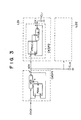
- Fig. 3 is a block diagram showing a structure of a clock distributing circuit according to the first embodiment of the present invention.
- the clock distributing circuit comprises an external clock input terminal EXCK (this also represents a clock type), a clock distribution output circuit CKSP1, and at least one load circuit LD1, LD2, and so forth.
- the clock distribution output circuit CKSP1 is connected to the external clock input terminal EXCK.
- the load circuits LD1, LD2, and so forth receive the clock from the clock distribution output circuit CKSP1 through a global clock line GCK (this also represents a clock type).
- All or part of the load circuits LD1, LD2, and so forth have a distributed clock input circuit CKSP2 (LD1 and LD2 in Fig. 1).
- a clock is input to the distributed clock input circuit CKSP2 through the global clock line GCK.
- the clock that is output from the distributed clock input circuit CKSP2 is supplied to an internal clock line ICK1 (that also represents a clock type) of the load circuit so as to drive a load capacitance CL1.
- ICK1 that also represents a clock type of the load circuit so as to drive a load capacitance CL1.
- the clock distribution output circuit CKSP1 is composed of a phase difference - voltage converting circuit (hereinafter referred to as a PDVC) and a voltage control type delay circuit (hereinafter referred to as a VCD).
- the PDVC converts a phase difference into a voltage.
- a clock input terminal i of the clock distribution output circuit CKSP1 is connected to a first input terminal i1 of the PDVC and a input terminal i of the VCD.
- a clock output terminal o of the clock distribution output circuit CKSP1 is connected to an output terminal o of the VCD and an input terminal i2 of the PDVC.
- An output terminal o of the PDVC is connected to a control terminal c of the VCD.
- the clock distribution output circuit CKSP1 has a so-called delay locked loop circuit (hereinafter referred to as a DLL circuit).
- the DLL circuit is for example described in Reference 2.
- Figs. 4 and 5 show examples of structures of the PDV and the VCD (that have no relation with the Reference 2), respectively.
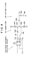
- the PDVC is composed of a phase difference detecting circuit PDD1 (that may be a phase/frequency difference detecting circuit PFDD2 that will be described later), a charge pump CP1, and a low pass filter LPF1.
- PDD1 phase difference detecting circuit
- PFDD2 phase/frequency difference detecting circuit
- LPF1 low pass filter
- the phase difference detecting circuit PDD1 is composed of a D-type flip-flop 41a and two AND gates 41b and 41c.
- the logic level of an input clock i1 supplied to a D input terminal of the D-type flip-flop 41a is detected when the logic level of a feed-back clock i2 supplied from the VCD becomes high.
- Output signal Q and Q/ are supplied to the AND gates 41b and 41c that are opened with the feed-back clock i2. (Although the negative logic of Q is denoted by Q bar (Q) in the accompanying drawings, Q/ is used instead thereof for easy notation).
- the logic level of an output signal UP supplied from the AND gate 41b becomes "H” only when the input clock i1 has a phase with an advance against the phase of the feed-back clock i2 after the lading edge of the input clock i1 to the leading edge of the input clock i2.
- the logic level of an output signal DW of the AND gate 41c becomes "H” only when the feed-back clock has a phase with an advance against the phase of the input clock i1 after the leading edge of the feed-back clock i2 to the leading edge of the input clock i1.
- the charge pump CP1 is composed of two current sources 42a and 42b, two switching transistors 42c and 42d, and an inverter 42e.
- the logic level of the signal UP is "H”
- the signal UP is supplied to a gate of the PMOS transistor 42c through the inverter 42e.
- the PMOS transistor 42c is turned on and a current is charged to the low pass filter LPF1.
- the logic level of the signal DW is "H”
- the signal DW is supplied to a gate of the NMOS transistor 42d.
- the NMOS transistor 42d is turned on a current is discharged from the low pass filter LPF1.
- the low pass filter LPF1 is composed of two resistors 43a and 43b and a condenser 43c. For simplicity, the description of the operation of the low pass filter LPF1 is omitted.
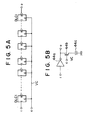
- the VCD is composed of a plurality of delay cells DLC1 that are cascade connected and of which a control voltage VC is supplied in common to control terminals of the delay cells DLC1.
- each of the delay cells DLC1 is composed of an inverter 44a, an NMOS transistor 44b, and a condenser 44c.
- the NMOS transistor 44b and the condenser 44c are connected in series between an output terminal of the inverter 44a and the ground.
- the control voltage VC varies, the time constant of a charging/discharging circuit composed of the NMOS transistor 44b and the condenser 44c varies.
- the output variation speed of the inverter 44a varies, thereby varying the delay time of the entire VCD.
- the distributed clock input circuit CKSP2 disposed in each of the load circuit LD1, LD2, and so forth includes a known PLL circuit that has the PFDVC and the VDO.
- PFDVC is composed of a phase/frequency difference detecting circuit PFDD2 (that may be the phase difference detecting circuit PDD1 shown in Fig. 4), a charge pump CP2, and a low pass filter LPF2 (the structures of the charge pump CP2 and the low pass filter LPF2 are the same as those shown in Fig. 4).
- the phase/frequency difference detecting circuit PFDD2 is composed of a D-type flip-flop 61a, a D-type flip-flop 61b, and a NOR gate 61c. A D input terminal of the D-type flip-flop 61a is pulled up.
- An input clock i1 is supplied to a clock input terminal of the D-type flip-flop 61a.
- a D input terminal of the D-type flip-flop 61b is pulled up.
- An input clock i2 is supplied to a clock input terminal of the D-type flip-flop 61b.
- Output signals Q/ of the flip-flops 61a and 61b are supplied to reset input terminals of the D-type flip-flops 61a and 61b through the NOR gate 61c.
- the logic level of the Q output of the D-type flip-flop 61a becomes "H" from the leading edge of the input clock I1 to the reading edge of the feed-back clock i2.
- the logic level of the Q output of the D-type flip-flop 61b becomes "H" from the leading edge of the feed-back clock i2 to the leading edge of the input clock i1.
- the D-type flip-flop 61a outputs the signal UP or the D-type flip-flop 61b outputs the signal DOWN.
- the period of which the logic levels of the signals UP and DOWN in the phase difference detecting circuit PDD1 are "H” is 1/2 clock period or less.
- the period of which the logic levels of the signals UP and DOWN in the phase/frequency difference detecting circuit PFDD2 is close to one clock period.
- Fig. 7 is a schematic diagram showing a structure of the VCO.
- the VCO shown in Fig. 7 is composed of a plurality of delay cells DLC1 and an inverter INV 71 that are connected in a ring shape so as to structure a ring oscillator.
- a control voltage VC is supplied in common to control terminals of the delay cells DLC1.
- the clock distributing circuit comprises the clock distribution output circuit (which includes the DLL circuit) and the distributed clock input circuit (that includes the PLL circuit).
- Fig. 8 is a schematic diagram showing wave forms of clocks for explaining the operation of the first embodiment.
- a phase offset error ⁇ 0 is present between the external clock at the external clock input terminal EXCK and a global clock on the global clock line GCK.
- the PDVC of the clock distribution output signal CKSP1 converts the error ⁇ 0 into a voltage.
- the VCD is controlled corresponding to this voltage so that ⁇ 0 decreases.
- time elapses to some extent (at time t1) the clock skew between the external clock and the global clock disappears.
- the VCD delays the input clock.
- the frequency of the external clock is almost the same as the frequency of the global clock.
- the output clock supplied to the internal clock line ICK1 is synchronized with the clock on the global clock line GCK.
- the frequency of the internal clock is matched with the frequency of the global clock.
- the phase difference between these clocks is removed.
- the frequency matching operation of the distributed clock output circuit CKSP2 is performed before the follow-up operation of the DLL circuit of the clock distribution output circuit CKSP1 is completed (in other words, the frequency matching operation is performed before time tl).
- the follow-up time (t0 to t1) of the DLL circuit is shorter than that of the PLL circuit.
- the stable time after the external clock is supplied until the clock supplied to the entire system becomes stable almost depends on the follow-up time (t4 to t2) of the PLL circuit of the distributed clock input circuit CKSP2.
- the clock distribution output circuit that includes the DLL circuit supplies the global clock that synchronizes with the external clock to each load circuit.
- each load circuit has the distributed clock input circuit that supplies a clock that synchronizes with the global clock thereto.
- Fig. 9 is a block diagram showing a structure of a clock distributing circuit according to a second embodiment of the present invention.
- the clock dividing circuit according to the second embodiment comprises a clock distribution output circuit CKSP 201 that distributes a clock to load circuits LD1, LD2, and so forth.
- the clock distribution output circuit CKSP 201 supplies a clock that synchronizes with an external clock that is supplied from an external clock input terminal EXCK to the load circuits LD1, LD2, and so forth through an inner global clock line GCK.
- the clock distribution output circuit CKSP 201 does not include a DLL circuit, but a PLL circuit.
- a distributed clock input circuit CKSP 202 is disposed.
- the distributed clock input circuit CKSP 202 generates an internal clock that synchronizes with a global clock on the global clock line GCK and supplies the internal clock to the load circuits LD1, LD2, and so forth.
- the distributed clock input circuit CKSP 202 does not include the PLL circuit, but the DLL circuit.
- the clock distribution output circuit CKSP 201 that includes the PLL circuit according to the second embodiment has the same PFDVC and VCO that are the same as those of the distributed clock input circuit CKSP2 that includes the PLL circuit according to the first embodiment.
- the distributed clock input circuit CKSP 201 that includes the DLL circuit according to the second embodiment has the same PDVC and VCD as those of the clock distribution output circuit CKSP1 that includes the DLL circuit according to the first embodiment.
- the clock distribution output circuit CKSP 201 that includes the PLL circuit performs the follow-up operation.
- the clock skew between the external clock supplied from the external clock input terminal EXCK and the global clock on the global clock line GCK is removed.
- the DLL circuit included in the distributed clock input circuit CKSP 202 removes the phase difference between the internal clock on the internal clock line ICK1 of each of the load circuits LD1, LD2, and so forth and the global clock on the global clock line GCK.
- the clock stable time of the second embodiment is slightly longer than the clock stable time of the first embodiment.
- the clock distributing circuit according to the second embodiment has the following advantages in operation over the structure of which two PLL circuits are cascade connected.
- the phase error response of the distributed clock input circuit including the DLL circuit is much faster than that of the structure including the PLL circuit.
- the clock distribution output circuit CKSP 201 removes a large skew between the external clock and the global clock.
- the distributed clock input circuit CKSP 202 only removes skews that take place in a small circuit range of the load circuits LD1, LD2, and so forth. Consequently, the distributed clock input circuit CKSP 202 can remove the skew between the global clock and the internal clock in a very short time. As a result, the startup time of the system can be remarkably reduced in comparison with the structure of which two PLL circuits are cascade connected.
- the first staged clock distribution output circuit CKSP 201 includes the PLL circuit that has a wider operating frequency range (thus, the system can be more easily designed) than the structure including the DLL circuit, the restriction of the external clock can be alleviated and a wide operating frequency range can be obtained.
- the PLL circuit information of the frquency difference between the input clock and the output clock is input to the VCO.
- the VCO oscillates corresponding to the information of the frequency difference.
- information of the phase difference between the input clock and the output clock is input to the VCD.
- the VCD controls the delay amount corresponding to the information of the phase difference.
- the PLL circuit controls the oscillation frequency of the output clock of the VCO.
- the DLL circuit controls the delay amount of the VCD.
- the clock distribution output circuit CKSP 201 including the PLL circuit is disposed in common with the load circuits LD1, LD2, and so forth.
- the distributed clock input circuit CKSP 202 including the DLL circuit is disposed on the input stage of each of the load circuits LD1, LD2, and so forth.
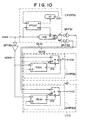
- Fig. 10 is a block diagram showing a structure of a clock distributing circuit according to a third embodiment of the present invention.
- the clock distributing circuit comprises an external clock input terminal EXCK, a clock distribution output circuit CKSP 31, and a plurality of load circuits LD1, LD2, and so forth.
- the clock distribution output circuit CKSP 31 distributes and supplies a global clock that has a phase with an advance against the phase of an external clock to a first global clock line GCK1.
- the clock distribution output circuit CKSP 31 distributes and supplies a clock that has a phase with a delay against the phase of the external clock to a second global clock line GCK2.
- the number of load circuits is two.
- a first global clock and a second global clock on a first global clock line GCK1 and a second global clock line GCK2 are supplied to input stages of the load circuits LD1, LD2, and so forth.
- a 0-th global clock (external clock) on a 0-th global clock line GCK0 supplied from the external clock input terminal EXCK is supplied to the input stages of the load circuits LD1, LD2, and so forth.
- Distributed clock input circuits CKSP 321, CKSP 322, and so forth that generate and supply internal clocks to the load circuits LD1, LD2, and so forth are disposed.
- buffer circuits BFF 30 to BFF 32 may be disposed on the 0-th to second global clock lines GCK0 to GCK2 so that the 0-th to second global clock lines GCK0 to GCK2 are driven by the respective buffer circuits BFF 30 to BFF 32.
- the clock distribution output circuit CKSP 31 is composed of a PFDVC (that controls two voltages), a VCO, and a VCD.
- a first output terminal o1 of the PFDVC is connected to a control terminal VC of the VCO.
- a second output terminal o2 of the PFDVC is connected to a control terminal VC of the VCD.
- a first input terminal i1 of the PFDVC and an input terminal i of the VDC are connected to an external clock input terminal EXCK through an input terminal i of the clock distribution output circuit CKSP 31.
- an output terminal o of the VCO is connected to a second input terminal i2.
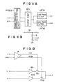
- the PFDVC according to the third embodiment has the same structure as that shown in Fig. 6. However, as shown in Fig. 11(a), the PFDVC according to the third embodiment has low pass filters LPF 31 and LPF 32 that are connected to a charge pump CP 3 and that outputs signals to the VCO and the VCD unlike with the structure shown in Fig. 6. In the third embodiment, two low pass filters are functionally required. Thus, it is possible to use a structure of which a connected point of a resistor 11b and a condenser 11c that are connected in series between a first output terminal o1 and the ground is a second output terminal o2. In the third embodiment, the cutoff frequency of the low pass filter LPF 32 is lower than the cutoff frequency of the low pass filter LPF 31.
- the VCO is for example a ring shaped oscillator of which a plurality of delay cells are connected in a ring shape as shown in Fig. 7.
- the VCD has a structure of which a plurality of the same cells shown in Fig. 5(a) are cascade connected.
- an output signal is obtained from a predetermined staged delay cell of the VCD.
- a global clock that has a predetermined phase difference against the external clock is obtained.
- a first global clock that has a phase with an advance against the phase of the external clock by 45° is output from an output terminal o1.
- a second global clock that has a phase with a delay against the phase of the external clock by 45° is output from a second output terminal o2 of the VCD.
- each of the distributed clock input circuits CKSP 321, CKSP 322, and so forth disposed in the input stages of the load circuits LD1, LD2, and so forth is composed of a PDVC and a voltage control type phase shifter (hereinafter referred to as a PS).
- a first input terminal i1 of the PS is connected to a first global clock line GCK1.
- a second input terminal i2 is connected to a second global clock line GCK2.
- a first input terminal i1 of the PDVC is connected to the 0-th global clock line GCK0.
- a second input terminal i2 of the PDVC is connected to an output terminal o of the PS and an output terminal O of the distributed clock input circuit.
- an output terminal o of the PDVC is connected to a control terminal c of the PS.
- the PDVC of each of the distributed clock input circuits CKSP 321, CKSP 322, and so forth may have the structure shown in Fig. 4.
- the PS weights and adds the voltages supplied to the input terminals i1 and i2 corresponding to the voltage supplied to the control terminal c and outputs the result to the output terminal o.
- the wave forms of the voltages at the input terminal i1 and the input terminal i2 are combined at the output terminal o. Consequently, an output clock with a predetermined phase difference against the external clock is obtained.
- an internal clock with a phase difference that ranges from -45° to +45° against the external clock and that is almost proportional to the voltage supplied to the control terminal c is obtained and supplied to the internal clock lines ICK1, ICK2, and so forth.
- the distributed clock input circuits CKSP 321, CKSP 322, and so forth that has the PS that combines two global clocks with a phase difference and supplies an output pulse have much excellent voltage phase converting characteristics than that of the distributed clock input circuit structure having the PLL circuit and DLL circuit composed of voltage control type delay cells.
- Fig. 12 is a schematic diagram showing a structure of a PS (voltage control type phase shifter).
- the PS is composed of two buffer means B51 and B52, two transfer gates T51 and T52, and a differential buffer means OP.
- Each of the buffer means B51 and B52 are composed of an amplifier with a gain of 1 or 2.
- the differential buffer means OP is composed of a differential amplifier with a small gain.
- the difference between the control voltage c supplied to the PS and a reference voltage VREF is obtained by the differential buffer means OP.
- a positive phase difference voltage VCG and a reverse phase difference voltage VCGB are supplied to control terminals of the transfer gates T51 and T52, respectively.
- a first global clock with a phase that advances by 45° against the phase of the external clock is supplied to the buffer means B51.
- a second global clock with a phase that delays by 45° against the phase of the external clock is supplied to the buffer means B52.
- Amplified signals that are output from the buffer means B51 and B52 are supplied to the transfer gates T51 and T52, respectively.
- the amplified signals are weighted by the transfer gates T51 and T52 and supplied to the output gate o.
- a combined signal of the amplified signals is obtained as an internal clock from the output terminal o.
- Fig. 13 is a schematic diagram showing wave forms of clocks for explaining the operation of the third embodiment.
- the PLL circuit (composed of the PFDVC and the VCO) of the clock distribution output circuit CKSP 31 follows the external clock EXCK and locks the oscillation frequency of the VCO so that it accords with the frequency of the external clock.
- the VCD of the clock distribution output circuit CKSP 31 is composed of the same delay cells as those of the VCO, the same DC control voltage as that supplied to the control terminal c of the VCO is supplied to the control terminal c.
- the phase shift amount of each delay cell of the VCD becomes stable with a predetermined amount.
- the VCO is composed of the same delay cells of four staged differential amplifying circuits, a clock with a phase shifted by 45° is obtained from each delay cell of the VCD.
- the cutoff frequencies of the low pass filters LPF 31 and LPF 32 of the PFDVC are varied.
- the feed-back clock of the PFDVC is treated as an output clock of the VCO.
- the output clock of the VCD in the follow-up state is treated as output clocks GCK1 and GCK2 of the circuit CKSP 31.
- the characteristics of which the PLL circuit has a faster follow-up speed than the DLL circuit can be effectively used.
- the output clock of the PLL circuit is used as the output clock of the clock distribution output circuit CKSP 31, the jitter becomes large.
- the distributed clock input circuits CKSP 321, CKSP 322, and so forth operate as follows.
- the DLL circuit is composed of the PDVC and the PS.
- the DLL circuit removes the clock skew between the output clock ICK and the 0-th global clock GCK 0.
- the phase of the output clock ICK supplied from the DLL circuit has an excessive delay against the phase of the 0-th global clock
- the output voltage of the PDVC rises (or drops) and thereby the weighting of the clock supplied from the input terminal il (namely, the global clock GCK1 that has a phase with an advance) increases.
- the wave form of the output clock supplied from the PS becomes similar to the wave form of the clock supplied from the input terminal il.
- the excessive delay of the phase of the output clock supplied from the distributed clock input circuits CKSP 321, CKSP 322, and so forth is compensated.
- the internal clocks ICK1, ICK2, and so forth distributed to the load circuits LD1, LD2, and so forth, respectively, are synchronized with the 0-th global clock GCK0 (thus, the external clock). Consequently, the skew between the external clock and the internal clock is removed.
- the time period T1 is shorter than the follow-up time of the PLL circuit (composed of the PFDVC and the VCO) in the clock distribution output circuit CKSP 31.
- the PFDVC and the VCD in the clock distribution output circuit CKSP 31 are those of the PLL circuit as the feed-back clock.
- the PFDVC and the VCD can be treated as those of the DLL circuit.
- the portion treated as the DLL circuit starts removing the phase difference.
- the clock supplied from the PLL circuit has a jitter and has not completely followed the external clock, the global clocks GCK1 and GCK2 supplied from the VCD become stable (see the operation of the second embodiment).
- the phase difference between each of the internal clocks ICK1, ICK2, and so forth of the load circuits LD1, LD2, and so forth and the external clock (the 0-th global clock GCK0) is removed within a time period T2 after the global clocks GCK1 and GCK2 become stable.
- the time period T2 for which the DLL circuit removes the phase error is satisfactorily shorter than the follow-up time of the conventional PLL circuit.
- the skew removing operation of the distributed clock input circuits CKSP 321, CKSP 322, and so forth are performed partially in parallel with the follow-up operation of the PLL circuit of the clock distribution output circuit CKSP 31.
- the stable time period (T1 + T2) until each internal clock becomes stable is almost equal to or less than the follow-up time of the PLL circuit of the clock distribution output circuit CKSP 321.
- the clock distributing circuit has the clock distribution output circuit that generates a first global clock that synchronizes with the external clock and that has a phase with an advance against the phase thereof and a second global clock that synchronizes with the external clock and that has a phase with a delay against the phase thereof.
- the clock distributing circuit according to the third embodiment has the distributed clock input circuit including the DLL circuit that supplies the internal clocks to the load circuits corresponding to the first global clock, the second global clock, and the external clock.
Description
- This application claims the priority right under EPC Art. 88 Par. 1, of Japanese Patent Application No. Hei 07-179081 filed on July 14, 1995.
- The present invention relates to a clock distributing circuit for distributing clock pulses (hereinafter referred to as a clock) to a plurality of circuits. In particular, the present invention relates to a clock distributing circuit for use with a circuit system on which a plurality of semiconductor chips with a chip size of 1 cm2 or more are disposed.
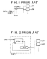
- Fig. 1 is a schematic diagram showing a conventional clock distributing circuit. In Fig. 2, the clock distributing circuit comprises an external clock input terminal EXEC and a plurality of clock buffers CKBFF1, CKBFF2, and so forth. The external clock input terminal EXCK inputs an external clock. The clock buffers CKBFF1, CKBFF2, and so forth are connected in a tree shape. The clock is input from the external clock input terminal EXCK and branched to a plurality of load circuits LD1, LD2, and so forth by the clock buffers CKBFF1, CKBFF2, and so forth.
- To drive the many load circuits LD1, LD2, and so forth that have large capacitance, the load circuits LD1, LD2, and so forth should be connected to the clock buffers CKBFF1, CKBFF2, and so forth in such a manner that the drive capacity thereof increase successively. In the clock distributing circuit connected with a plurality of clock buffers CKBFF1, CKBFF2, and so forth, due to delay of the clock in the clock buffers CKBFF1, CKBFF2, and so forth, a large clock skew takes place between the external clock input terminal EXCK and each of the clock input terminals of the load circuits LD1, LD2, and so forth.
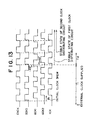
- To solve the skew, a method of which a clock buffer CKBFF having a PLL (Phase-Locked Loop) shown in Fig. 3 has been proposed as in
Reference 1. -
Reference 1, "Nikkei Microdevice", Nikkei PB Company, pp. 81 to 85, February 1993. - In Fig. 2, the CKBFF is disposed between an external clock input terminal EXEC and each of load circuits LD1, LD2, and so forth. The CKBFF has a PLL circuit composed of a phase/frequency difference - voltage converting circuit (hereinafter referred to as a PFDVC) that converts a phase/frequency difference into a DC voltage and a voltage control type oscillator (hereinafter referred to as a VCO). The output clock of the clock buffer CKBFF is supplied to each of the clock input terminals of the load circuit LD1, LD2, and so forth.
- The PLL circuit causes the input clock of the external clock input terminal EXCK to synchronize with the output clock of the clock buffer CKBFF, thereby minimizing the phase difference thereof. Thus, when the output portion of the VCO has a buffer circuit with a high drive performance, the clock can be distributed to the load circuits LD1, LD2, and so forth without a clock skew caused by a delay of the clock in the clock buffer CKBFF.
- However, even if the method using the clock buffer CKBFF with the PLL circuit is employed, the following problem takes place.
- In lines that connect the clock buffer CKBFF and each of the load circuits LD1, LD2, and so forth, a transmission delay due to a stray resistance and a stray capacitance takes place, thereby causing a clock skew.
- When the load circuits LD1, LD2, and so forth are formed on respective semiconductor chips, each of the load circuits LD1, LD2, and so forth requires a clock buffer. When conventional clock buffers are used, they cause clock skews. In such a large scaled circuit, even if one clock buffer with the PLL circuit as a clock buffer on the distribution side is disposed, the clock skew cannot be satisfactorily reduced.
- To solve this problem, in addition to the common clock buffer with a PLL circuit, a local clock buffer with a PLL circuit may be disposed for each load circuit. However, when clock buffers with PLL circuits are cascade connected, the stable time of the clock of the load circuit depends on the sum of the follow-up time of each clock buffer. (The follow-up time is a time period until the follow-up operation of the PLL circuit effectively operates against a variation of the input clock in the condition that the phase difference between the input clock and the output clock is less than a predetermined value.) Thus, the system does not quickly operate.
- Moreover, although a PLL circuit for a clock buffer in a load circuit operates for removing the phase difference between the input clock and the output clock, it can be said that the PLL circuit does not well operate for removing the clock skew due to a transmission delay on lines connected between the common clock buffer and the load circuit.
- An object of the present invention is to provide a clock distributing circuit that can reduce the clock skew and the clock stable time and that can be used for a large scale circuit.
- According to a first aspect of the present invention, a clock distributing circuit comprises a clock distribution output circuit for inputting an external clock, outputting a first clock, and distributing the first clock to each of a plurality of load circuits, and one or more distributed clock input circuits disposed on input stages of one or more load circuits and adapted for inputting the first clock and outputting a local clock, characterised in that, the clock distribution output circuit further comprises first synchronization means for synchronizing the first clock with the external clock and the one or more distributed clock input circuits include second synchronization means for synchronizing the local clock with the first clock, wherein one of said first and second synchronization means includes a phase difference - voltage converting circuit for converting the phase difference between an input clock and an output clock into a voltage and a voltage control delay circuit for delaying the input clock corresponding to an output voltage of the phase difference - voltage converting circuit and for outputting the delayed input clock.
- In this manner, a so-called DLL circuit structure is used for one of the clock distribution output circuit or a distributed clock input circuit. When the other of the circuits is a PLL circuit that has a conventional synchronous structure, the disadvantages of the DLL circuit and the PLL circuit are compensated. Thus, the advantages of these circuits can be effectively obtained.
- Thus, the first clock is coarsely controlled by the clock distribution circuit and the first synchronization means so that the first clock synchronizes with the external clock. The frequency difference and the phase difference against the external clock are removed by the distributed clock input circuit and the second synchronization means. Thus, the skew difference removed by each circuit is decreased. Consequently, the jitter is decreased. In addition to the decrease of the skew removing time, the synchronization of the first clock with the external clock is performed partially in parallel with the synchronization of the local clock with the first clock. Thus, the system startup time can be reduced in comparison with the conventional structure in which PLL circuits are multiply staged.
- In addition, the load of each circuit is reduced. A clock with a higher frequency can be distributed. Thus, the clock stable time of each load circuit becomes short.
- Such a clock distributing circuit may be configured such that the first clock has a phase with an advance relative to the phase of the external clock, the clock distribution output circuit outputs a second clock that has a phase with a delay relative to the phase of the external clock, which is distributed to each of the load circuits and the one or more distributed clock input circuits receive the second clock and external clock, wherein said first synchronization means comprises said phase difference voltage converting circuit, in the form of a phase/frequency difference - voltage converting circuit for converting the phase/frequency difference between the external clock and the first clock into a voltage and outputting a first control voltage and a second control voltage, said voltage control delay circuit, being configured to delay the external clock in accordance with the second control voltage, and a voltage control oscillator for generating the second clock in accordance with the first control voltage and wherein each second synchronization means includes a phase-difference voltage converting circuit for converting a phase difference between the external clock and the local clock that is output from a distributed clock input circuit into a voltage and a voltage control phase shifter for generating the local clock from the first and second clocks in accordance with an output voltage of said phase difference - voltage converting circuit.
- In this arrangement, the clock distribution output circuit outputs the first clock and the second clock. The first clock synchronizes with the external clock and has a phase with a delay against the phase thereof. The first clock and the second clock are distributed to each of the load circuits. A distributed clock input circuit disposed at an input stage of one of the load circuits outputs a local clock that synchronizes with the external clock corresponding to the first clock, the second clock and the external clock. At this point, the voltage control phase shifter of the distributed clock input circuit varies a weighted combined amount of the first clock and the second clock corresponding to an output voltage of the phase difference - voltage converting circuit, thereby generating the local clock. In other words, each load is divided and dispersed to two stages. A synchronizing circuit having a phase shifter with a higher linearity of phase difference - voltage converting characteristics is disposed in the later stage.
- The first or second synchronization means may further comprise a frequency dividing circuit, so as to form a frequency synthesizer.
- Embodiments of the invention will now be described with reference to the accompanying drawings.
-
- Fig. 1 is a block diagram showing a structure of a conventional circuit (No. 1);
- Fig. 2 is a block diagram showing a structure of a conventional circuit (No. 2);
- Fig. 3 is a block diagram showing a structure of a first embodiment of the invention;
- Fig. 4 is a block diagram showing a structure of a phase/frequency difference - voltage converting circuit (No. 1);
- Fig. 5 is a block diagram showing a structure of a voltage control type delay circuit;
- Fig. 6 is a block diagram showing a structure of a phase difference - voltage converting circuit;
- Fig. 7 is a block diagram showing a structure of a voltage control type oscillator;
- Fig. 8 is a schematic diagram showing wave forms of signals of the first embodiment of the present invention;
- Fig. 9 is a block diagram showing a structure of a second embodiment of the present invention;
- Fig. 10 is a block diagram showing a structure of a third embodiment;
- Fig. 11 is a block diagram showing a structure of a phase/ frequency difference - voltage converting circuit (No. 2);
- Fig. 12 is a block diagram showing a structure of a voltage control type phase shifter;
- Fig. 13 is a schematic diagram showing waves forms of signals of the third embodiment.
-
- Next, with reference to the accompanying drawings, a clock distributing circuit according to a first embodiment of the present invention will be described.
- Fig. 3 is a block diagram showing a structure of a clock distributing circuit according to the first embodiment of the present invention. In Fig. 3, the clock distributing circuit comprises an external clock input terminal EXCK (this also represents a clock type), a clock distribution output circuit CKSP1, and at least one load circuit LD1, LD2, and so forth. The clock distribution output circuit CKSP1 is connected to the external clock input terminal EXCK. The load circuits LD1, LD2, and so forth receive the clock from the clock distribution output circuit CKSP1 through a global clock line GCK (this also represents a clock type).
- All or part of the load circuits LD1, LD2, and so forth have a distributed clock input circuit CKSP2 (LD1 and LD2 in Fig. 1). A clock is input to the distributed clock input circuit CKSP2 through the global clock line GCK. The clock that is output from the distributed clock input circuit CKSP2 is supplied to an internal clock line ICK1 (that also represents a clock type) of the load circuit so as to drive a load capacitance CL1. (In this example, it is assumed that since each load circuit is composed of a MOS transistor and so forth, only the load capacitance is considered. However, of course, a resistor component may be formed.)
- The clock distribution output circuit CKSP1 is composed of a phase difference - voltage converting circuit (hereinafter referred to as a PDVC) and a voltage control type delay circuit (hereinafter referred to as a VCD). The PDVC converts a phase difference into a voltage. A clock input terminal i of the clock distribution output circuit CKSP1 is connected to a first input terminal i1 of the PDVC and a input terminal i of the VCD. A clock output terminal o of the clock distribution output circuit CKSP1 is connected to an output terminal o of the VCD and an input terminal i2 of the PDVC. An output terminal o of the PDVC is connected to a control terminal c of the VCD.
- In other words, the clock distribution output circuit CKSP1 has a so-called delay locked loop circuit (hereinafter referred to as a DLL circuit). The DLL circuit is for example described in Reference 2.
- Reference 2 - Stefanous Sidiropoulos, et. al, "A CMOS 500 Mbps/pin synchronous point to point link interface", IEEE, 1994 Symposium on VLSI Circuits Digest of Technical Papers, pp. 43-44, June, 1994.
- Figs. 4 and 5 show examples of structures of the PDV and the VCD (that have no relation with the Reference 2), respectively.
- In Fig. 4, the PDVC is composed of a phase difference detecting circuit PDD1 (that may be a phase/frequency difference detecting circuit PFDD2 that will be described later), a charge pump CP1, and a low pass filter LPF1.
- The phase difference detecting circuit PDD1 is composed of a D-type flip-flop 41a and two AND
gates 41b and 41c. The logic level of an input clock i1 supplied to a D input terminal of the D-type flip-flop 41a is detected when the logic level of a feed-back clock i2 supplied from the VCD becomes high. Output signal Q and Q/ are supplied to the ANDgates 41b and 41c that are opened with the feed-back clock i2. (Although the negative logic of Q is denoted by Q bar (Q) in the accompanying drawings, Q/ is used instead thereof for easy notation). Thus, the logic level of an output signal UP supplied from the AND gate 41b becomes "H" only when the input clock i1 has a phase with an advance against the phase of the feed-back clock i2 after the lading edge of the input clock i1 to the leading edge of the input clock i2. On the other hand, the logic level of an output signal DW of the ANDgate 41c becomes "H" only when the feed-back clock has a phase with an advance against the phase of the input clock i1 after the leading edge of the feed-back clock i2 to the leading edge of the input clock i1. - The charge pump CP1 is composed of two
current sources transistors inverter 42e. When the logic level of the signal UP is "H", the signal UP is supplied to a gate of thePMOS transistor 42c through theinverter 42e. Thus, thePMOS transistor 42c is turned on and a current is charged to the low pass filter LPF1. When the logic level of the signal DW is "H", the signal DW is supplied to a gate of theNMOS transistor 42d. Thus, theNMOS transistor 42d is turned on a current is discharged from the low pass filter LPF1. - As shown in Fig. 4, the low pass filter LPF1 is composed of two
resistors condenser 43c. For simplicity, the description of the operation of the low pass filter LPF1 is omitted. - On the other hand, as shown in Fig. 5(a), the VCD is composed of a plurality of delay cells DLC1 that are cascade connected and of which a control voltage VC is supplied in common to control terminals of the delay cells DLC1. As shown in Fig. 5(b), each of the delay cells DLC1 is composed of an
inverter 44a, an NMOS transistor 44b, and acondenser 44c. The NMOS transistor 44b and thecondenser 44c are connected in series between an output terminal of theinverter 44a and the ground. When the control voltage VC varies, the time constant of a charging/discharging circuit composed of the NMOS transistor 44b and thecondenser 44c varies. Thus, the output variation speed of theinverter 44a varies, thereby varying the delay time of the entire VCD. - Returning to Fig. 3, the distributed clock input circuit CKSP2 disposed in each of the load circuit LD1, LD2, and so forth includes a known PLL circuit that has the PFDVC and the VDO.
- Next, an example of the structure of the PFDVC will be described. As shown in Fig. 6, PFDVC is composed of a phase/frequency difference detecting circuit PFDD2 (that may be the phase difference detecting circuit PDD1 shown in Fig. 4), a charge pump CP2, and a low pass filter LPF2 (the structures of the charge pump CP2 and the low pass filter LPF2 are the same as those shown in Fig. 4). The phase/frequency difference detecting circuit PFDD2 is composed of a D-type flip-flop 61a, a D-type flip-flop 61b, and a NOR gate 61c. A D input terminal of the D-type flip-flop 61a is pulled up. An input clock i1 is supplied to a clock input terminal of the D-type flip-flop 61a. A D input terminal of the D-type flip-flop 61b is pulled up. An input clock i2 is supplied to a clock input terminal of the D-type flip-flop 61b. Output signals Q/ of the flip-flops 61a and 61b are supplied to reset input terminals of the D-type flip-flops 61a and 61b through the NOR gate 61c. The logic level of the Q output of the D-type flip-flop 61a becomes "H" from the leading edge of the input clock I1 to the reading edge of the feed-back clock i2. Alternatively, the logic level of the Q output of the D-type flip-flop 61b becomes "H" from the leading edge of the feed-back clock i2 to the leading edge of the input clock i1. Thus, the D-type flip-flop 61a outputs the signal UP or the D-type flip-flop 61b outputs the signal DOWN. The period of which the logic levels of the signals UP and DOWN in the phase difference detecting circuit PDD1 are "H" is 1/2 clock period or less. On the other hand, the period of which the logic levels of the signals UP and DOWN in the phase/frequency difference detecting circuit PFDD2 is close to one clock period.
- Fig. 7 is a schematic diagram showing a structure of the VCO. The VCO shown in Fig. 7 is composed of a plurality of delay cells DLC1 and an inverter INV 71 that are connected in a ring shape so as to structure a ring oscillator. A control voltage VC is supplied in common to control terminals of the delay cells DLC1.
- As described above, the clock distributing circuit according to the first embodiment comprises the clock distribution output circuit (which includes the DLL circuit) and the distributed clock input circuit (that includes the PLL circuit).
- Fig. 8 is a schematic diagram showing wave forms of clocks for explaining the operation of the first embodiment. Just after an external clock is supplied, a phase offset error Θ0 is present between the external clock at the external clock input terminal EXCK and a global clock on the global clock line GCK. The PDVC of the clock distribution output signal CKSP1 converts the error Θ0 into a voltage. The VCD is controlled corresponding to this voltage so that Θ0 decreases. Thus, when time elapses to some extent (at time t1), the clock skew between the external clock and the global clock disappears. In addition, the VCD delays the input clock. Thus, just after the external clock is supplied, the frequency of the external clock is almost the same as the frequency of the global clock.
- With the follow-up operation of the PLL circuit in the distributed clock input circuit CKSP2, the output clock supplied to the internal clock line ICK1 is synchronized with the clock on the global clock line GCK. At this point, in a broad sense, the frequency of the internal clock is matched with the frequency of the global clock. Thereafter, the phase difference between these clocks is removed. As described above, since the clock distribution output circuit CKSP1 causes the frequency of the global clock to match the frequency of the external clock just after the external clock is supplied, the frequency matching operation of the distributed clock output circuit CKSP2 is performed before the follow-up operation of the DLL circuit of the clock distribution output circuit CKSP1 is completed (in other words, the frequency matching operation is performed before time tl). Generally, the follow-up time (t0 to t1) of the DLL circuit is shorter than that of the PLL circuit. The stable time after the external clock is supplied until the clock supplied to the entire system becomes stable almost depends on the follow-up time (t4 to t2) of the PLL circuit of the distributed clock input circuit CKSP2.
- As described above, according to the first embodiment, the clock distribution output circuit that includes the DLL circuit supplies the global clock that synchronizes with the external clock to each load circuit. In addition, each load circuit has the distributed clock input circuit that supplies a clock that synchronizes with the global clock thereto. Thus, the following effects can be obtained.
- (1) Since the loads of the clock distribution output circuit and each of the distributed clock input circuits are reduced in comparison with the conventional structure of which all load circuits are driven by the clock distributing circuit that has one PLL circuit. Thus, the clock skew due to the stray capacitance or the like is decreased. Consequently, a clock with a higher frequency than the of the conventional structure can be supplied to a large scaled circuit.
- (2) Almost when the synchronizing operation of the DLL circuit of the clock distribution output circuit starts, the follow-up operation of the PLL circuit of the distributed clock input circuit starts. Thus, the clock of the system becomes stable in a short time. Consequently, the system can be quickly started up. Generally, the PLL circuit more can quickly removes a large phase/frequency difference than the DLL circuit. However, when two staged PLL circuits are connected, after the first staged PLL circuit becomes stable, the second staged PLL circuit starts the follow-up operation. Thus, it takes a time until the system starts up. When the system starts up, it is difficult to reduce the phase/frequency difference to a desired level. On the other hand, the DLL circuit can quickly adjust a frequency difference. In addition, the DLL circuit can precisely adjust small phase difference. However, the DLL circuit takes a longer time to remove a large phase difference than the PLL circuit. Thus, when a plurality of DLL circuits are disposed, it takes a long time until the system ptarts up.Consequently, to accomplish the above-described effects, it is preferable to provide the clock distribution output circuit including the DLL circuit that supplies the global clock that synchronizes with the external clock to each load circuit and each load circuit including the PLL circuit that supplies a clock that synchronizes with the global clock to the load circuit as with the first embodiment.
- (3) Since the distributed clock input circuit including the PLL circuit is disposed for each load circuit, the phase error difference (due to the time constant of the low pass filter) of the PLL circuit can be optimized for each load circuit. Thus, the jitter of the clock can be reduced. If necessary, a frequency diving circuit is disposed between the VCO and the PFDVC in the distributed clock input circuit of a particular load circuit so as to form a frequency synthesizer. Thus, a clock with a frequency several times higher than the frequency of the global clock can be supplied.
- (4) When a delay circuit corresponding to the clock skew due to the global clock line is disposed in a feed-back loop from the VCD to the PDVC in the clock distribution output circuit, the clock skew due to the line from the clock distribution output circuit to the load circuit can be reduced.
-
- Next, with reference to the accompanying drawings, a clock distributing circuit according to a second embodiment will be described.
- Fig. 9 is a block diagram showing a structure of a clock distributing circuit according to a second embodiment of the present invention. In Fig. 9, the clock dividing circuit according to the second embodiment comprises a clock distribution output circuit CKSP 201 that distributes a clock to load circuits LD1, LD2, and so forth. The clock distribution output circuit CKSP 201 supplies a clock that synchronizes with an external clock that is supplied from an external clock input terminal EXCK to the load circuits LD1, LD2, and so forth through an inner global clock line GCK.
- However, the clock distribution output circuit CKSP 201 according to the second embodiment does not include a DLL circuit, but a PLL circuit.
- On the other hand, in the input stage of all or part of the load circuits LD1, LD2, and so forth of the second embodiment, a distributed clock input circuit CKSP 202 is disposed. The distributed clock input circuit CKSP 202 generates an internal clock that synchronizes with a global clock on the global clock line GCK and supplies the internal clock to the load circuits LD1, LD2, and so forth.
- However, the distributed clock input circuit CKSP 202 according to the second embodiment does not include the PLL circuit, but the DLL circuit.
- The clock distribution output circuit CKSP 201 that includes the PLL circuit according to the second embodiment has the same PFDVC and VCO that are the same as those of the distributed clock input circuit CKSP2 that includes the PLL circuit according to the first embodiment. The distributed clock input circuit CKSP 201 that includes the DLL circuit according to the second embodiment has the same PDVC and VCD as those of the clock distribution output circuit CKSP1 that includes the DLL circuit according to the first embodiment.
- In the second embodiment, when an external clock is input, the clock distribution output circuit CKSP 201 that includes the PLL circuit performs the follow-up operation. Thus, the clock skew between the external clock supplied from the external clock input terminal EXCK and the global clock on the global clock line GCK is removed. The DLL circuit included in the distributed clock input circuit CKSP 202 removes the phase difference between the internal clock on the internal clock line ICK1 of each of the load circuits LD1, LD2, and so forth and the global clock on the global clock line GCK.
- Thus, in the second embodiment, until the follow-up operation of the PLL circuit of the clock distribution output circuit CKSP 201 progresses to some extent and the frequency difference between the external clock and the global clock becomes small, the distributed clock input circuit CKSP 202 cannot effectively remove the skew.
- Thus, the clock stable time of the second embodiment is slightly longer than the clock stable time of the first embodiment. However, the clock distributing circuit according to the second embodiment has the following advantages in operation over the structure of which two PLL circuits are cascade connected.
- In other words, when the phase error is small, the phase error response of the distributed clock input circuit including the DLL circuit is much faster than that of the structure including the PLL circuit. In addition, the clock distribution output circuit CKSP 201 removes a large skew between the external clock and the global clock. Thus, the distributed clock input circuit CKSP 202 only removes skews that take place in a small circuit range of the load circuits LD1, LD2, and so forth. Consequently, the distributed clock input circuit CKSP 202 can remove the skew between the global clock and the internal clock in a very short time. As a result, the startup time of the system can be remarkably reduced in comparison with the structure of which two PLL circuits are cascade connected.
- In addition, since the first staged clock distribution output circuit CKSP 201 includes the PLL circuit that has a wider operating frequency range (thus, the system can be more easily designed) than the structure including the DLL circuit, the restriction of the external clock can be alleviated and a wide operating frequency range can be obtained. Generally, in the PLL circuit, information of the frquency difference between the input clock and the output clock is input to the VCO. Thus, the VCO oscillates corresponding to the information of the frequency difference. On the other hand, in the DLL circuit, information of the phase difference between the input clock and the output clock is input to the VCD. Thus, the VCD controls the delay amount corresponding to the information of the phase difference. In other words, the PLL circuit controls the oscillation frequency of the output clock of the VCO. On the other hand, the DLL circuit controls the delay amount of the VCD. Thus, since the operating frequency range of the PLL circuit is wider than the operating frequency range of the DLL circuit. Consequently, a system with the PLL circuit can be more easily designed than a system with the DLL circuit.
- As described above, according to the second embodiment, the clock distribution output circuit CKSP 201 including the PLL circuit is disposed in common with the load circuits LD1, LD2, and so forth. In addition, the distributed clock input circuit CKSP 202 including the DLL circuit is disposed on the input stage of each of the load circuits LD1, LD2, and so forth. Thus, the clock distributing circuit according to the second embodiment has following effects.
- (1) The loads that the clock distribution output circuit and the distributed clock input circuit drive can be reduced. Thus, a clock with a high operating frequency can be obtained as with the first embodiment.
- (2) Since the first staged clock distribution output circuit includes the PLL circuit, the clock distributing circuit can operate in a wide frequency range.
- (3) The clock distribution output circuit remove a large clock skew. In addition, the distributed clock input circuit disposed in each of the load circuits removes the clock skew in the load circuit. Thus, the clock distributing circuit according to the second embodiment can quickly remove the clock skew. Consequently, the system startup time of the second embodiment is shorter than that of the structure of which two PLL circuits are cascade connected and that of the structure of which two DLL circuits are cascade connected.
- (4) When a delay circuit corresponding to the clock skew due to the global clock line or the like is disposed in the feed-back loop from the VCO to the PFDVC of the clock distribution output circuit, the clock skew due to the line from the clock distribution output circuit to the load circuit can be reduced.
-
- Next, with reference to the accompanying drawings, a clock distributing circuit according to a third embodiment of the present invention will be described.
- Fig. 10 is a block diagram showing a structure of a clock distributing circuit according to a third embodiment of the present invention.
- The clock distributing circuit according to the third embodiment comprises an external clock input terminal EXCK, a clock distribution output circuit CKSP 31, and a plurality of load circuits LD1, LD2, and so forth. The clock distribution output circuit CKSP 31 distributes and supplies a global clock that has a phase with an advance against the phase of an external clock to a first global clock line GCK1. In addition, the clock distribution output circuit CKSP 31 distributes and supplies a clock that has a phase with a delay against the phase of the external clock to a second global clock line GCK2. In this example, the number of load circuits is two.
- A first global clock and a second global clock on a first global clock line GCK1 and a second global clock line GCK2 are supplied to input stages of the load circuits LD1, LD2, and so forth. In addition, a 0-th global clock (external clock) on a 0-th global clock line GCK0 supplied from the external clock input terminal EXCK is supplied to the input stages of the load circuits LD1, LD2, and so forth. Distributed clock input circuits CKSP 321, CKSP 322, and so forth that generate and supply internal clocks to the load circuits LD1, LD2, and so forth are disposed. If necessary, buffer circuits BFF 30 to BFF 32 may be disposed on the 0-th to second global clock lines GCK0 to GCK2 so that the 0-th to second global clock lines GCK0 to GCK2 are driven by the respective buffer circuits BFF 30 to BFF 32.
- The clock distribution output circuit CKSP 31 is composed of a PFDVC (that controls two voltages), a VCO, and a VCD.
- A first output terminal o1 of the PFDVC is connected to a control terminal VC of the VCO. A second output terminal o2 of the PFDVC is connected to a control terminal VC of the VCD. A first input terminal i1 of the PFDVC and an input terminal i of the VDC are connected to an external clock input terminal EXCK through an input terminal i of the clock distribution output circuit CKSP 31. In addition, an output terminal o of the VCO is connected to a second input terminal i2.
- The PFDVC according to the third embodiment has the same structure as that shown in Fig. 6. However, as shown in Fig. 11(a), the PFDVC according to the third embodiment has low pass filters LPF 31 and LPF 32 that are connected to a charge pump CP 3 and that outputs signals to the VCO and the VCD unlike with the structure shown in Fig. 6. In the third embodiment, two low pass filters are functionally required. Thus, it is possible to use a structure of which a connected point of a
resistor 11b and a condenser 11c that are connected in series between a first output terminal o1 and the ground is a second output terminal o2. In the third embodiment, the cutoff frequency of the low pass filter LPF 32 is lower than the cutoff frequency of the low pass filter LPF 31. - The VCO is for example a ring shaped oscillator of which a plurality of delay cells are connected in a ring shape as shown in Fig. 7.
- On the other hand, the VCD has a structure of which a plurality of the same cells shown in Fig. 5(a) are cascade connected. In this case, an output signal is obtained from a predetermined staged delay cell of the VCD. Thus, a global clock that has a predetermined phase difference against the external clock is obtained. In the third embodiment, a first global clock that has a phase with an advance against the phase of the external clock by 45° is output from an output terminal o1. In addition, a second global clock that has a phase with a delay against the phase of the external clock by 45° is output from a second output terminal o2 of the VCD.
- Returning to Fig. 10, each of the distributed clock input circuits CKSP 321, CKSP 322, and so forth disposed in the input stages of the load circuits LD1, LD2, and so forth is composed of a PDVC and a voltage control type phase shifter (hereinafter referred to as a PS).
- A first input terminal i1 of the PS is connected to a first global clock line GCK1. A second input terminal i2 is connected to a second global clock line GCK2. A first input terminal i1 of the PDVC is connected to the 0-th global clock line GCK0. A second input terminal i2 of the PDVC is connected to an output terminal o of the PS and an output terminal O of the distributed clock input circuit. In addition, an output terminal o of the PDVC is connected to a control terminal c of the PS.
- The PDVC of each of the distributed clock input circuits CKSP 321, CKSP 322, and so forth may have the structure shown in Fig. 4.
- The PS weights and adds the voltages supplied to the input terminals i1 and i2 corresponding to the voltage supplied to the control terminal c and outputs the result to the output terminal o. Thus, the wave forms of the voltages at the input terminal i1 and the input terminal i2 are combined at the output terminal o. Consequently, an output clock with a predetermined phase difference against the external clock is obtained.
- In the third embodiment, an internal clock with a phase difference that ranges from -45° to +45° against the external clock and that is almost proportional to the voltage supplied to the control terminal c is obtained and supplied to the internal clock lines ICK1, ICK2, and so forth.
- As described above, it is known that the distributed clock input circuits CKSP 321, CKSP 322, and so forth that has the PS that combines two global clocks with a phase difference and supplies an output pulse have much excellent voltage phase converting characteristics than that of the distributed clock input circuit structure having the PLL circuit and DLL circuit composed of voltage control type delay cells.
- Fig. 12 is a schematic diagram showing a structure of a PS (voltage control type phase shifter). In Fig. 12, the PS is composed of two buffer means B51 and B52, two transfer gates T51 and T52, and a differential buffer means OP. Each of the buffer means B51 and B52 are composed of an amplifier with a gain of 1 or 2. Likewise, the differential buffer means OP is composed of a differential amplifier with a small gain. The difference between the control voltage c supplied to the PS and a reference voltage VREF is obtained by the differential buffer means OP. As weighting coefficients, a positive phase difference voltage VCG and a reverse phase difference voltage VCGB are supplied to control terminals of the transfer gates T51 and T52, respectively. A first global clock with a phase that advances by 45° against the phase of the external clock is supplied to the buffer means B51. A second global clock with a phase that delays by 45° against the phase of the external clock is supplied to the buffer means B52. Amplified signals that are output from the buffer means B51 and B52 are supplied to the transfer gates T51 and T52, respectively. The amplified signals are weighted by the transfer gates T51 and T52 and supplied to the output gate o. Thus, a combined signal of the amplified signals is obtained as an internal clock from the output terminal o.
- Fig. 13 is a schematic diagram showing wave forms of clocks for explaining the operation of the third embodiment. When the external clock is supplied, the PLL circuit (composed of the PFDVC and the VCO) of the clock distribution output circuit CKSP 31 follows the external clock EXCK and locks the oscillation frequency of the VCO so that it accords with the frequency of the external clock.
- On the other hand, the VCD of the clock distribution output circuit CKSP 31 is composed of the same delay cells as those of the VCO, the same DC control voltage as that supplied to the control terminal c of the VCO is supplied to the control terminal c. Thus, when the PLL circuit performs the locking operation, the phase shift amount of each delay cell of the VCD becomes stable with a predetermined amount. For example, when the VCO is composed of the same delay cells of four staged differential amplifying circuits, a clock with a phase shifted by 45° is obtained from each delay cell of the VCD. Thus, when an output signal is extracted from a predetermined stage of cascade connected delay cells of the VCD, a clock with a phase that has an advance by 45° against the external clock (this clock is the first global clock GCK1) and a clock with a phase that has a delay by 45° against the external clock (this clock is the second global clock GCK2) are obtained as shown in Fig. 13.
- In the third embodiment, the cutoff frequencies of the low pass filters LPF 31 and LPF 32 of the PFDVC are varied. The feed-back clock of the PFDVC is treated as an output clock of the VCO. In addition, the output clock of the VCD in the follow-up state is treated as output clocks GCK1 and GCK2 of the circuit CKSP 31. Thus, the characteristics of which the PLL circuit has a faster follow-up speed than the DLL circuit can be effectively used. In addition, when the output clock of the PLL circuit is used as the output clock of the clock distribution output circuit CKSP 31, the jitter becomes large.
- In Fig. 11, when buffer circuits BFF 30, BFF 31, and BFF 32 are disposed, the delay amounts thereof are much smaller than the time period equivalent to the
phase 45° of the clock. - On the other hand, the distributed clock input circuits CKSP 321, CKSP 322, and so forth operate as follows.
- In the distributed clock input circuits CKSP 321, CKSP 322, and so forth, the DLL circuit is composed of the PDVC and the PS. The DLL circuit removes the clock skew between the output clock ICK and the 0-th
global clock GCK 0. - When the phase ICK of the output clock of the DLL circuit has an excessive advance against the phase of a 0-th global clock GCK0, the output voltage of the PDVC drops (rises). Thus, the weighting of the clock supplied from the input terminal i2 increases and thereby the wave form of the output clock of the PS becomes similar to the wave form of the clock supplied from the input terminal i2. Consequently, the excessive advance of the output clock supplied from the distributed clock input circuits CKSP 321, CKSP 322, and so forth is compensated.
- On the other hand, when the phase of the output clock ICK supplied from the DLL circuit has an excessive delay against the phase of the 0-th global clock, the output voltage of the PDVC rises (or drops) and thereby the weighting of the clock supplied from the input terminal il (namely, the global clock GCK1 that has a phase with an advance) increases. Thereby, the wave form of the output clock supplied from the PS becomes similar to the wave form of the clock supplied from the input terminal il. Thus, the excessive delay of the phase of the output clock supplied from the distributed clock input circuits CKSP 321, CKSP 322, and so forth is compensated.
- As described above, the internal clocks ICK1, ICK2, and so forth distributed to the load circuits LD1, LD2, and so forth, respectively, are synchronized with the 0-th global clock GCK0 (thus, the external clock). Consequently, the skew between the external clock and the internal clock is removed.
- Next, the stable time after the external clock is supplied until the internal clocks ICK1, ICK2, and so forth distributed to respective load circuits LD1, LD2, and so forth become stable will be described.
- It takes a predetermined time period T1 after the external clock is supplied until the global clocks GCK1 and GCK2 become stable. However, the time period T1 is shorter than the follow-up time of the PLL circuit (composed of the PFDVC and the VCO) in the clock distribution output circuit CKSP 31. The PFDVC and the VCD in the clock distribution output circuit CKSP 31 are those of the PLL circuit as the feed-back clock. However, the PFDVC and the VCD can be treated as those of the DLL circuit. Thus, even if the PLL circuit does not completely follow the external clock, when the frequency difference between the external clock and the the clock supplied from the VCO becomes small (for example, the frequency difference becomes smaller than the cutoff frequency of the low pass filter LPF 32), the portion treated as the DLL circuit starts removing the phase difference. Even if the clock supplied from the PLL circuit has a jitter and has not completely followed the external clock, the global clocks GCK1 and GCK2 supplied from the VCD become stable (see the operation of the second embodiment).
- In the DLL circuit composed of the PDVC and the PS of each of the distributed clock input circuits CKSP 321, CKSP 322, and so forth, the phase difference between each of the internal clocks ICK1, ICK2, and so forth of the load circuits LD1, LD2, and so forth and the external clock (the 0-th global clock GCK0) is removed within a time period T2 after the global clocks GCK1 and GCK2 become stable. In the DLL circuit, since a frequency error does not constantly take place between the input clock and the output clock, the time period T2 for which the DLL circuit removes the phase error is satisfactorily shorter than the follow-up time of the conventional PLL circuit.
- Thus, the skew removing operation of the distributed clock input circuits CKSP 321, CKSP 322, and so forth are performed partially in parallel with the follow-up operation of the PLL circuit of the clock distribution output circuit CKSP 31. Thus, the stable time period (T1 + T2) until each internal clock becomes stable is almost equal to or less than the follow-up time of the PLL circuit of the clock distribution output circuit CKSP 321.
- According to the third embodiment, the clock distributing circuit has the clock distribution output circuit that generates a first global clock that synchronizes with the external clock and that has a phase with an advance against the phase thereof and a second global clock that synchronizes with the external clock and that has a phase with a delay against the phase thereof. In addition, the clock distributing circuit according to the third embodiment has the distributed clock input circuit including the DLL circuit that supplies the internal clocks to the load circuits corresponding to the first global clock, the second global clock, and the external clock. Thus, the clock distributing circuit according to the third embodiment has the following effects.
- (1) Since the distributed clock input circuit disposed for each load circuit distributes and supplies an internal clock and removes a skew, the load of the clock distributing circuits is reduced. Thus, a clock with a high operating frequency can be supplied. Consequently, the clock skew can be quickly removed.
- (2) The first global clock that has a phase with an advance against the phase of the external clock and a second global clock that has a phase with a delay against the phase of the external clock are supplied to the voltage control type phase shifter PS (with excellent voltage -phase conversion characteristics in linearlity) of the distributed clock input circuit. In addition, the phase shift amount of the voltage control type phase shifter is controlled with a control voltage corresponding to the phase difference between the external clock and the internal clock so as to generate the internal clock. Thus, the control voltage is suppressed from improperly varying and the jitter is reduced.
- (3) The external clock is input to the PDVC of the distributed clock input circuit directly or through only a buffer means. In addition, the external clock is delayed with the control voltage generated by the PLL circuit of the clock distribution output circuit so as to generate the first and second global clocks. The first and second global clocks are supplied to the voltage control type phase shifter of the distributed clock input circuit. Thus, the follow-up operation of the PLL circuit of the clock distribution output circuit and the clock skew removing operation of the distributed clock input circuit are performed partially in parallel. Consequently, the stable time after the external clock is supplied until the clock supplied to the system becomes stable becomes short.
-
-
- (1) According to the clock distributing circuit of the present invention, the circuit is divided into a plurality of portions. A clock with a high frequency and a small jitter is supplied as an external clock to each portion. The external clock is quickly distributed to each portion. Thus, the clock distributing circuit according to the present invention can be effectively used for a semiconductor circuit integrated on a large area chip, a system board, a SIM, or DIM on which a large number of semiconductor circuits are disposed, and a multi-chip module (MCM).
- (2) The clock line used in each embodiment can be substituted with a complementary clock line that transmits complementary clock pulses. In this case, as with an ECL, a pair of complementary pulses are input and a pair of complementary pulses are output. In addition, the present invention can be applied for distributing pulses with a duty ratio of 50 % as well as clock pulses. The term "clock" in "what is claimed is" of the present patent application includes the meaning of single and complementary clocks. In addition, the application of pulses includes the meaning of pulses other than clock pulses.
- (3) If necessary, a frequency dividing circuit may be disposed in the PLL circuit according to the second embodiment or the third embodiment so that the clock distributing circuit operates with a frequency synthesizer.
- (4) It should be noted that the PFDVC, PDVC, VCO, and VCD are not limited to the structures described in the above-described first to third embodiments. For example, the PFDVC may be composed of an F-V converter with an integrating circuit or composed of an up-down counter and a D/A converter. In addition, the PDVC may be composed of an analog multiplying circuit.
- (5) In the third embodiment, a structure for outputting two same control voltages may be used instead of the PFDVC for outputting two types of control voltages.
-
- Although the present invention has been shown and described with respect to best mode embodiments thereof, it should be understood by those skilled in the art that the foregoing and various other changes, omissions, and additions in the form and detail thereof may be made therein without departing from the scope of the present invention.
Claims (7)
- A clock distributing circuit, comprising:characterised in that:a clock distribution output circuit (CKSP1, CKSP201, CKSP301) for inputting an external clock, outputting a first clock, and distributing the first clock to each of a plurality of load circuits (LD1, LD2); andone or more of distributed clock input circuits (CKSP2, CKSP202, CKSP321, CKSP322) disposed on input stages of one or more of the load circuits (LD1, LD2) and adapted for inputting the first clock and outputting a local clock,wherein one of said first and second synchronization means includes:the clock distribution output circuit (CKSP1, CKSP201, CKSP301) further comprises first synchronization means for synchronizing the first clock with the external clock; andthe one or more distributed clock input circuits (CKSP2, CKSP202, CKSP321, CKSP322) include second synchronization means for synchronizing the local clock with the first clock;a phase difference - voltage converting circuit (PDVC) for converting the phase difference between an input clock and an output clock into a voltage; anda voltage control delay circuit (VCD) for delaying the input clock corresponding to an output voltage of the phase difference - voltage converting circuit (PDVC) and for outputting the delayed input clock.
- A clock distributing circuit according to claim 1, wherein the first synchronization means comprises said phase difference - voltage converting circuit (PDVC) and said voltage control delay circuit (DLC1).
- A clock distributing circuit according to claim 2, wherein:wherein said first synchronization means comprises:the first clock has a phase with an advance relative to the phase of the external clock;the clock distribution output circuit (CKSP31) outputs a second clock that has a phase with a delay relative to the phase of the external clock, which is distributed to each of the one or more load circuits (LD1, LD2); andthe one or more distributed clock input circuits (CKSP321, CKSP322) receive the second clock and external clock;and wherein each second synchronization means includes:said phase difference voltage converting circuit, in the form of a phase/frequency difference - voltage converting circuit (PFDVC) for converting the phase/frequency difference between the external clock and the first clock into a voltage and outputting a first control voltage and a second control voltage;said voltage control delay circuit (VCD), being configured to delay the external clock in accordance with the second control voltage; anda voltage control oscillator (VCO) for generating the second clock in accordance with the first control voltage;a phase-difference voltage converting circuit (PDVC) for converting a phase difference between the external clock and the local clock that is output from a distributed clock input circuit (CKSP321, CKSP322) into a voltage; anda voltage control phase shifter (PS) for generating the local clock from the first and second clocks in accordance with an output voltage of said phase difference - voltage converting circuit (PDVC).
- A clock distributing circuit according to claim 2 or 3, wherein the first synchronization means further comprises a frequency dividing circuit.
- A clock distributing circuit according to claim 2, wherein each second synchronization means comprises:a phase/frequency difference - voltage converting circuit (PFVDC) for converting a phase difference between the first clock and a local clock output by a distributed clock input circuit (CKSP2) into a control voltage; anda voltage control oscillator (VCO) for generating the local clock in accordance with said control voltage.
- A clock distributing circuit according to claim 5, wherein at least one second synchronization means further comprises a frequency dividing circuit disposed between the phase/frequency difference - voltage converting circuit (PFVDC) and the voltage control oscillator (VCO).
- A clock distributing circuit according to claim 3, wherein the first and second control voltages are the same.
Applications Claiming Priority (3)
| Application Number | Priority Date | Filing Date | Title |
|---|---|---|---|
| JP179081/95 | 1995-07-14 | ||
| JP17908195A JP3403551B2 (en) | 1995-07-14 | 1995-07-14 | Clock distribution circuit |
| JP17908195 | 1995-07-14 |
Publications (3)
| Publication Number | Publication Date |
|---|---|
| EP0753808A2 EP0753808A2 (en) | 1997-01-15 |
| EP0753808A3 EP0753808A3 (en) | 1998-05-13 |
| EP0753808B1 true EP0753808B1 (en) | 2004-10-06 |
Family
ID=16059759
Family Applications (1)
| Application Number | Title | Priority Date | Filing Date |
|---|---|---|---|
| EP96305040A Expired - Lifetime EP0753808B1 (en) | 1995-07-14 | 1996-07-09 | Clock distributing circuit |
Country Status (5)
| Country | Link |
|---|---|
| US (1) | US5751665A (en) |
| EP (1) | EP0753808B1 (en) |
| JP (1) | JP3403551B2 (en) |
| DE (1) | DE69633539T2 (en) |
| TW (1) | TW301823B (en) |
Families Citing this family (53)
| Publication number | Priority date | Publication date | Assignee | Title |
|---|---|---|---|---|
| DE19627634C1 (en) * | 1996-07-09 | 1997-07-24 | Siemens Ag | CMOS circuit of CMOS blocks in bit parallel data paths esp. semiconductor circuits |
| US6115318A (en) | 1996-12-03 | 2000-09-05 | Micron Technology, Inc. | Clock vernier adjustment |
| US5940608A (en) | 1997-02-11 | 1999-08-17 | Micron Technology, Inc. | Method and apparatus for generating an internal clock signal that is synchronized to an external clock signal |
| US5920518A (en) | 1997-02-11 | 1999-07-06 | Micron Technology, Inc. | Synchronous clock generator including delay-locked loop |
| US5946244A (en) | 1997-03-05 | 1999-08-31 | Micron Technology, Inc. | Delay-locked loop with binary-coupled capacitor |
| US5907589A (en) * | 1997-04-10 | 1999-05-25 | Motorola, Inc. | GHZ range frequency divider in CMOS |
| US6173432B1 (en) | 1997-06-20 | 2001-01-09 | Micron Technology, Inc. | Method and apparatus for generating a sequence of clock signals |
| US5983013A (en) * | 1997-06-30 | 1999-11-09 | Sun Microsystems, Inc. | Method for generating non-blocking delayed clocking signals for domino logic |
| US5953284A (en) | 1997-07-09 | 1999-09-14 | Micron Technology, Inc. | Method and apparatus for adaptively adjusting the timing of a clock signal used to latch digital signals, and memory device using same |
| US6011732A (en) | 1997-08-20 | 2000-01-04 | Micron Technology, Inc. | Synchronous clock generator including a compound delay-locked loop |
| US5940609A (en) * | 1997-08-29 | 1999-08-17 | Micorn Technology, Inc. | Synchronous clock generator including a false lock detector |
| US5926047A (en) * | 1997-08-29 | 1999-07-20 | Micron Technology, Inc. | Synchronous clock generator including a delay-locked loop signal loss detector |
| US6101197A (en) | 1997-09-18 | 2000-08-08 | Micron Technology, Inc. | Method and apparatus for adjusting the timing of signals over fine and coarse ranges |
| KR100269316B1 (en) * | 1997-12-02 | 2000-10-16 | 윤종용 | Delayed locked loop & phase locked loop merged with synchronous delay circuit |
| US5867453A (en) * | 1998-02-06 | 1999-02-02 | Taiwan Semiconductor Manufacturing Co., Ltd. | Self-setup non-overlap clock generator |
| US6269451B1 (en) | 1998-02-27 | 2001-07-31 | Micron Technology, Inc. | Method and apparatus for adjusting data timing by delaying clock signal |
| US6016282A (en) | 1998-05-28 | 2000-01-18 | Micron Technology, Inc. | Clock vernier adjustment |
| US6338127B1 (en) | 1998-08-28 | 2002-01-08 | Micron Technology, Inc. | Method and apparatus for resynchronizing a plurality of clock signals used to latch respective digital signals, and memory device using same |
| US6349399B1 (en) * | 1998-09-03 | 2002-02-19 | Micron Technology, Inc. | Method and apparatus for generating expect data from a captured bit pattern, and memory device using same |
| US6279090B1 (en) | 1998-09-03 | 2001-08-21 | Micron Technology, Inc. | Method and apparatus for resynchronizing a plurality of clock signals used in latching respective digital signals applied to a packetized memory device |
| US6029250A (en) | 1998-09-09 | 2000-02-22 | Micron Technology, Inc. | Method and apparatus for adaptively adjusting the timing offset between a clock signal and digital signals transmitted coincident with that clock signal, and memory device and system using same |
| US6118314A (en) * | 1998-10-14 | 2000-09-12 | Vlsi Technology, Inc. | Circuit assembly and method of synchronizing plural circuits |
| JP3753355B2 (en) | 1998-11-10 | 2006-03-08 | 株式会社ルネサステクノロジ | Semiconductor device |
| US6430696B1 (en) | 1998-11-30 | 2002-08-06 | Micron Technology, Inc. | Method and apparatus for high speed data capture utilizing bit-to-bit timing correction, and memory device using same |
| US6717997B1 (en) * | 1998-12-01 | 2004-04-06 | International Business Machines Corporation | Apparatus and method for current demand distribution in electronic systems |
| US6374360B1 (en) | 1998-12-11 | 2002-04-16 | Micron Technology, Inc. | Method and apparatus for bit-to-bit timing correction of a high speed memory bus |
| US6470060B1 (en) | 1999-03-01 | 2002-10-22 | Micron Technology, Inc. | Method and apparatus for generating a phase dependent control signal |
| US6594772B1 (en) * | 2000-01-14 | 2003-07-15 | Hewlett-Packard Development Company, L.P. | Clock distribution circuitry to different nodes on integrated circuit with clock coupling circuitry to maintain predetermined phase relation between output and input of adjacent nodes |
| US6513149B1 (en) | 2000-03-31 | 2003-01-28 | International Business Machines Corporation | Routing balanced clock signals |
| US6566921B1 (en) * | 2000-08-03 | 2003-05-20 | International Business Machines Corporation | Apparatus and method for high resolution frequency adjustment in a multistage frequency synthesizer |
| US6963992B1 (en) * | 2000-09-28 | 2005-11-08 | Cypress Semiconductor Corp. | Method and apparatus to generate clock and control signals for over-clocking recovery in a PLL |
| US6760277B1 (en) * | 2001-04-06 | 2004-07-06 | Advanced Micro Devices, Inc. | Arrangement for generating multiple clocks in field programmable gate arrays of a network test system |
| US6801989B2 (en) | 2001-06-28 | 2004-10-05 | Micron Technology, Inc. | Method and system for adjusting the timing offset between a clock signal and respective digital signals transmitted along with that clock signal, and memory device and computer system using same |
| US6566924B2 (en) * | 2001-07-25 | 2003-05-20 | Hewlett-Packard Development Company L.P. | Parallel push algorithm detecting constraints to minimize clock skew |
| US6897699B1 (en) * | 2002-07-19 | 2005-05-24 | Rambus Inc. | Clock distribution network with process, supply-voltage, and temperature compensation |
| US7256633B1 (en) | 2003-05-01 | 2007-08-14 | Ample Communications, Inc. | Systems for implementing high speed and high integration chips |
| US6927615B2 (en) * | 2003-06-05 | 2005-08-09 | International Business Machines Corporation | Low skew, power efficient local clock signal generation system |
| US7168027B2 (en) | 2003-06-12 | 2007-01-23 | Micron Technology, Inc. | Dynamic synchronization of data capture on an optical or other high speed communications link |
| US6956415B2 (en) * | 2003-11-19 | 2005-10-18 | International Business Machines Corporation | Modular DLL architecture for generating multiple timings |
| US6952127B2 (en) * | 2003-11-21 | 2005-10-04 | Micron Technology, Inc. | Digital phase mixers with enhanced speed |
| US6982578B2 (en) * | 2003-11-26 | 2006-01-03 | Micron Technology, Inc. | Digital delay-locked loop circuits with hierarchical delay adjustment |
| US6982579B2 (en) * | 2003-12-11 | 2006-01-03 | Micron Technology, Inc. | Digital frequency-multiplying DLLs |
| US7009434B2 (en) * | 2003-12-12 | 2006-03-07 | Micron Technology, Inc. | Generating multi-phase clock signals using hierarchical delays |
| US7528638B2 (en) * | 2003-12-22 | 2009-05-05 | Micron Technology, Inc. | Clock signal distribution with reduced parasitic loading effects |
| US7274236B2 (en) * | 2005-04-15 | 2007-09-25 | Micron Technology, Inc. | Variable delay line with multiple hierarchy |
| US7368961B2 (en) * | 2005-12-22 | 2008-05-06 | Rambus Inc. | Clock distribution network supporting low-power mode |
| US7882384B2 (en) * | 2006-08-31 | 2011-02-01 | National Semiconductor Corporation | Setting and minimizing a derived clock frequency based on an input time interval |
| JP5321179B2 (en) * | 2008-04-11 | 2013-10-23 | 富士通株式会社 | Phase control device, phase control printed board, and control method |
| JP5387187B2 (en) | 2009-07-10 | 2014-01-15 | 富士通株式会社 | Clock signal distribution device |
| US9160349B2 (en) | 2009-08-27 | 2015-10-13 | Micron Technology, Inc. | Die location compensation |
| WO2011046845A2 (en) | 2009-10-15 | 2011-04-21 | Rambus Inc. | Signal distribution networks and related methods |
| EP2902866B1 (en) | 2014-02-04 | 2018-03-07 | Hittite Microwave LLC | System ready in a clock distribution chip |
| CN117348687B (en) * | 2023-12-06 | 2024-03-01 | 爱科微半导体(上海)有限公司 | Clock power supply stray optimization system and calibration, calibration and optimization method thereof |
Family Cites Families (7)
| Publication number | Priority date | Publication date | Assignee | Title |
|---|---|---|---|---|
| US5184027A (en) * | 1987-03-20 | 1993-02-02 | Hitachi, Ltd. | Clock signal supply system |
| IL89120A (en) * | 1988-02-17 | 1992-08-18 | Mips Computer Systems Inc | Circuit synchronization system |
| US5087829A (en) * | 1988-12-07 | 1992-02-11 | Hitachi, Ltd. | High speed clock distribution system |
| US5305451A (en) * | 1990-09-05 | 1994-04-19 | International Business Machines Corporation | Single phase clock distribution circuit for providing clock signals to multiple chip integrated circuit systems |
| JPH04373009A (en) * | 1991-06-21 | 1992-12-25 | Hitachi Ltd | Phase control method for clock signal |
| US5298866A (en) * | 1992-06-04 | 1994-03-29 | Kaplinsky Cecil H | Clock distribution circuit with active de-skewing |
| KR100293596B1 (en) * | 1993-01-27 | 2001-09-17 | 가나이 쓰도무 | Clock Distribution Circuit in LSI |
-
1995
- 1995-07-14 JP JP17908195A patent/JP3403551B2/en not_active Expired - Fee Related
-
1996
- 1996-07-09 EP EP96305040A patent/EP0753808B1/en not_active Expired - Lifetime
- 1996-07-09 DE DE69633539T patent/DE69633539T2/en not_active Expired - Lifetime
- 1996-07-11 TW TW085108431A patent/TW301823B/zh not_active IP Right Cessation
- 1996-07-21 US US08/678,860 patent/US5751665A/en not_active Expired - Lifetime
Also Published As
| Publication number | Publication date |
|---|---|
| JPH0934584A (en) | 1997-02-07 |
| EP0753808A2 (en) | 1997-01-15 |
| DE69633539D1 (en) | 2004-11-11 |
| EP0753808A3 (en) | 1998-05-13 |
| DE69633539T2 (en) | 2005-01-27 |
| US5751665A (en) | 1998-05-12 |
| JP3403551B2 (en) | 2003-05-06 |
| TW301823B (en) | 1997-04-01 |
Similar Documents
| Publication | Publication Date | Title |
|---|---|---|
| EP0753808B1 (en) | Clock distributing circuit | |
| US6392458B1 (en) | Method and apparatus for digital delay locked loop circuits | |
| US6784707B2 (en) | Delay locked loop clock generator | |
| US6316976B1 (en) | Method and apparatus for improving the performance of digital delay locked loop circuits | |
| US5410263A (en) | Delay line loop for on-chip clock synthesis with zero skew and 50% duty cycle | |
| US6509776B2 (en) | DLL circuit, semiconductor device using the same and delay control method | |
| US20020079937A1 (en) | Digital delay locked loop with wide dynamic range and fine precision | |
| KR100319607B1 (en) | Analog dll circuit | |
| JPH04217115A (en) | Integrated circuit for changing relation in phase between at least one clock phase output and reference clock | |
| US7902896B2 (en) | Phase mixer with adjustable load-to-drive ratio | |
| US5517147A (en) | Multiple-phase clock signal generator for integrated circuits, comprising PLL, counter, and logic circuits | |
| WO2004010579A1 (en) | Apparatus and method for duty cycle correction | |
| US6759886B2 (en) | Clock generating circuit generating a plurality of clock signals | |
| JPH11145816A (en) | Semiconductor device | |
| US6384647B1 (en) | Digital clock multiplier and divider with sychronization during concurrences | |
| US7605624B2 (en) | Delay locked loop (DLL) circuit for generating clock signal for memory device | |
| Liu et al. | Low-power clock-deskew buffer for high-speed digital circuits | |
| US7002383B1 (en) | Method and apparatus for synthesizing a clock signal using a compact and low power delay locked loop (DLL) | |
| US7952413B2 (en) | Clock generating circuit and clock generating method thereof | |
| US6147532A (en) | PLL circuit capable of preventing malfunction of FF circuits connected thereto and semiconductor integrated circuit including the PLL circuit | |
| US20030137333A1 (en) | Multiphase-clock processing circuit and clock multiplying circuit | |
| KR100853862B1 (en) | Frequency multiplier based delay locked loop | |
| US20070165476A1 (en) | Clock signal generating circuit | |
| KR100290592B1 (en) | Clock distributing circuit | |
| US6934349B2 (en) | Phase detector and phase locked loop circuit |
Legal Events
| Date | Code | Title | Description |
|---|---|---|---|
| PUAI | Public reference made under article 153(3) epc to a published international application that has entered the european phase |
Free format text: ORIGINAL CODE: 0009012 |
|
| AK | Designated contracting states |
Kind code of ref document: A2 Designated state(s): DE FR GB NL |
|
| PUAL | Search report despatched |
Free format text: ORIGINAL CODE: 0009013 |
|
| AK | Designated contracting states |
Kind code of ref document: A3 Designated state(s): DE FR GB NL |
|
| 17P | Request for examination filed |
Effective date: 19980723 |
|
| 17Q | First examination report despatched |
Effective date: 20021122 |
|
| GRAP | Despatch of communication of intention to grant a patent |
Free format text: ORIGINAL CODE: EPIDOSNIGR1 |
|
| GRAS | Grant fee paid |
Free format text: ORIGINAL CODE: EPIDOSNIGR3 |
|
| GRAA | (expected) grant |
Free format text: ORIGINAL CODE: 0009210 |
|
| AK | Designated contracting states |
Kind code of ref document: B1 Designated state(s): DE FR GB NL |
|
| REG | Reference to a national code |
Ref country code: GB Ref legal event code: FG4D |
|
| REF | Corresponds to: |
Ref document number: 69633539 Country of ref document: DE Date of ref document: 20041111 Kind code of ref document: P |
|
| PLBE | No opposition filed within time limit |
Free format text: ORIGINAL CODE: 0009261 |
|
| STAA | Information on the status of an ep patent application or granted ep patent |
Free format text: STATUS: NO OPPOSITION FILED WITHIN TIME LIMIT |
|
| ET | Fr: translation filed | ||
| 26N | No opposition filed |
Effective date: 20050707 |
|
| PGFP | Annual fee paid to national office [announced via postgrant information from national office to epo] |
Ref country code: GB Payment date: 20070704 Year of fee payment: 12 |
|
| PGFP | Annual fee paid to national office [announced via postgrant information from national office to epo] |
Ref country code: FR Payment date: 20070710 Year of fee payment: 12 |
|
| GBPC | Gb: european patent ceased through non-payment of renewal fee |
Effective date: 20080709 |
|
| REG | Reference to a national code |
Ref country code: FR Ref legal event code: ST Effective date: 20090331 |
|
| PG25 | Lapsed in a contracting state [announced via postgrant information from national office to epo] |
Ref country code: GB Free format text: LAPSE BECAUSE OF NON-PAYMENT OF DUE FEES Effective date: 20080709 |
|
| PG25 | Lapsed in a contracting state [announced via postgrant information from national office to epo] |
Ref country code: FR Free format text: LAPSE BECAUSE OF NON-PAYMENT OF DUE FEES Effective date: 20080731 |
|
| PGFP | Annual fee paid to national office [announced via postgrant information from national office to epo] |
Ref country code: NL Payment date: 20100716 Year of fee payment: 15 |
|
| PGFP | Annual fee paid to national office [announced via postgrant information from national office to epo] |
Ref country code: DE Payment date: 20100707 Year of fee payment: 15 |
|
| REG | Reference to a national code |
Ref country code: NL Ref legal event code: V1 Effective date: 20120201 |
|
| PG25 | Lapsed in a contracting state [announced via postgrant information from national office to epo] |
Ref country code: DE Free format text: LAPSE BECAUSE OF NON-PAYMENT OF DUE FEES Effective date: 20120201 |
|
| REG | Reference to a national code |
Ref country code: DE Ref legal event code: R119 Ref document number: 69633539 Country of ref document: DE Effective date: 20120201 |
|
| PG25 | Lapsed in a contracting state [announced via postgrant information from national office to epo] |
Ref country code: NL Free format text: LAPSE BECAUSE OF NON-PAYMENT OF DUE FEES Effective date: 20120201 |