US20030088602A1 - High-speed computation in arithmetic logic circuit - Google Patents
High-speed computation in arithmetic logic circuit Download PDFInfo
- Publication number
- US20030088602A1 US20030088602A1 US10/005,551 US555101A US2003088602A1 US 20030088602 A1 US20030088602 A1 US 20030088602A1 US 555101 A US555101 A US 555101A US 2003088602 A1 US2003088602 A1 US 2003088602A1
- Authority
- US
- United States
- Prior art keywords
- significant bits
- binary
- bit
- operand
- significant
- Prior art date
- Legal status (The legal status is an assumption and is not a legal conclusion. Google has not performed a legal analysis and makes no representation as to the accuracy of the status listed.)
- Abandoned
Links
Images
Classifications
-
- G—PHYSICS
- G06—COMPUTING; CALCULATING OR COUNTING
- G06F—ELECTRIC DIGITAL DATA PROCESSING
- G06F7/00—Methods or arrangements for processing data by operating upon the order or content of the data handled
- G06F7/38—Methods or arrangements for performing computations using exclusively denominational number representation, e.g. using binary, ternary, decimal representation
- G06F7/48—Methods or arrangements for performing computations using exclusively denominational number representation, e.g. using binary, ternary, decimal representation using non-contact-making devices, e.g. tube, solid state device; using unspecified devices
- G06F7/50—Adding; Subtracting
- G06F7/505—Adding; Subtracting in bit-parallel fashion, i.e. having a different digit-handling circuit for each denomination
- G06F7/506—Adding; Subtracting in bit-parallel fashion, i.e. having a different digit-handling circuit for each denomination with simultaneous carry generation for, or propagation over, two or more stages
- G06F7/507—Adding; Subtracting in bit-parallel fashion, i.e. having a different digit-handling circuit for each denomination with simultaneous carry generation for, or propagation over, two or more stages using selection between two conditionally calculated carry or sum values
-
- G—PHYSICS
- G06—COMPUTING; CALCULATING OR COUNTING
- G06F—ELECTRIC DIGITAL DATA PROCESSING
- G06F2207/00—Indexing scheme relating to methods or arrangements for processing data by operating upon the order or content of the data handled
- G06F2207/38—Indexing scheme relating to groups G06F7/38 - G06F7/575
- G06F2207/3804—Details
- G06F2207/3808—Details concerning the type of numbers or the way they are handled
- G06F2207/3812—Devices capable of handling different types of numbers
- G06F2207/3816—Accepting numbers of variable word length
Definitions
- the present invention is directed to digital data processing, and more particularly, to reducing the processing time for complex datapath arithmetic computations in time-sensitive digital processing applications.
- Arithmetic-logic data processing circuit have been designed for a wide range of applications and have been used in virtually every industry. Among many other, these applications include those implemented using programmed computer arrangements, discrete logic circuitry and semi-programmable logic components. For a variety of reasons, many of these applications have been directed to processing video data and have demanded completion of specified processing operations in minimal times. Some applications have further demanded a high-speed computing engine that can perform complex arithmetic computations in the same minimal time frame typically allocated for relatively simple arithmetic computations.
- Video-data processing is one example of the many applications requiring relatively complex computations. Many of these video-data-processing applications require a signal processing circuit that is capable of performing increasingly-complex mathematical functions at ever-increasing speeds. Unfortunately, achieving high data-processing speeds and manipulating digital data according to more complex mathematical operations requiring time-consuming datapath arithmetic computations are opposing tensions.
- Various video-data filters are used in specialized video signal processing techniques, such as compressing and decompressing video data in real time.
- Useful in some applications is a type of specialized video-data filter known as a “polyphase” filter.
- a polyphase filter is sometimes used to resize pixels by manipulating data stored to represent the horizontal and vertical lines used to refresh the display.
- the ratio of the number of output pixels to the number of input pixels is defined as a zoom-factor; whereas, for general purpose filtering, the number of output pixels equals the number of input pixels.
- the resizing operation is also known as expansion or up-sampling when the zoom factor is greater than one; otherwise, resizing operation is typically known as compression or down-sampling.
- the polyphase filter is implemented with its coefficients defined as a function of the position or phase of the pixel that is being processed.
- the polyphase filtering is implemented with a more unique architecture to accommodate the math required to achieve the precision; typically, this type of polyphase filtering is implemented in a form referred to as “polyphase-transposed” filtering.
- the polyphase filtering is implemented as a polyphase direct filter using a computational architecture that is more common with general purpose filtering such as finite-impulse-response (FIR) filtering.
- FIR finite-impulse-response
- custom logic circuits to process datapath arithmetic computations at a requisite speed is time-consuming, and costly, to implement and verify. There is a significant cost in connection with designing, manufacturing and maintaining the integrated circuits used to provide such functionality. Using conventional or library logic circuits is easier to implement and verify, thus less costly, but do not achieve the necessary operational speed when used in an straight-forward “off-the-shelf” operation.
- the requisite math associated with data processing filters is typically accomplished through a series of basic arithmetic operations.
- the series of computations is repeated for each pixel of a video display.
- the length of a pipeline stage in a computational datapath design is usually determined by the maximum number of arithmetic operations that can be achieved within a targeted clock cycle, the targeted clock cycle being determined from a the number of pixels that must be processed per unit of real time to support the video display.
- Efficiencies in the underlying repetitive elementary arithmetical computations that implement the higher-order mathematical operations are compounded through repetition into significant overall processing improvements.
- the present invention is directed to a data-processing circuit that addresses the above-mentioned challenges and that reduces the time otherwise required for implementing arithmetic computations.
- the present invention is exemplified in a number of implementations and applications, some of which are summarized below.
- the present invention is directed to arithmetic computational circuitry that implements basic arithmetic operations (e.g., addition and/or subtraction) as a series of sub-arithmetic operations and logical operations.
- basic arithmetic operations e.g., addition and/or subtraction
- the present invention is believed to be applicable to a variety of different types of filtering applications, and has been found to be particularly useful for video filtering applications and other applications benefiting from a data processing circuit that can add and subtract relatively large binary numbers in a relatively fast period of time.
- binary number arithmetic is implemented as a combination of arithmetic operations upon a portion of each binary number and logical operations involving further portions of the input binary numbers.
- the circuit arrangement is adapted to add a first binary operand of N bits and a second binary operand of M bits, N being greater than or equal to M.
- the circuit arrangement includes an adder coupled to a multiplexer circuit. A representative set of least-significant bits of the first and second binary operands are added together to produce a least-significant bits partial sum and a carryout.
- a logic circuit such as a 4-1 demultiplexer circuit or other similarly-functioning data-passing circuit, is arranged to produce, as an output, a most-significant bits partial sum by passing either a representative set of most-significant bits of the first binary operand, or an offset of the representative set of most-significant bits of the first binary operand.
- the data-passing circuit is responsive to selection data, the selection data being a function of the most-significant bit of the representative set of least-significant bits of the first binary operand.
- the circuit arrangement includes an M-bit adder, and the multiplexer circuit selects a N ⁇ M most-significant bits partial sum responsive to the M-bit adder carryout and the Mth bit of the first operand.
- each operand includes a sign bit as its respective most-significant bit
- the multiplexer circuit is configured to select either the N ⁇ M most significant bits of the first operand, the N ⁇ M most significant bits of the first operand incremented by one, or the N ⁇ M most significant bits of the first operand decremented by one.
- the above-characterized approaches are implemented as part of a pixel-data digital filter using for various filtering applications such as scaling and polyphase filtering.
- FIG. 1 illustrates a general block diagram of an example data-processing circuit, according to the present invention.
- FIG. 2 illustrates a general block diagram of an example functional datapath unit for a reconfigurable digital filter, according to the present invention.
- FIG. 3 illustrates an example data manipulation flow diagram through a datapath for a zoom computation of a polyphase direct filter operating in a panoramic mode, according to the present invention.
- FIG. 4 illustrates a block diagram of selection logic for accelerating a 24-bit addition computation within a digital filter, according to the present invention.
- FIG. 5A illustrates a block diagram of selection logic for accelerating a 25-bit addition computation within a digital filter, according to the present invention.
- FIG. 5B illustrates a block diagram of selection logic for determining an intermediate carryout within a 25-bit addition computation of a digital filter, according to the present invention.
- FIG. 5C illustrates a block diagram of selection logic for accelerating a 4-bit addition computation within a digital filter, according to the present invention.
- the present invention is believed to be applicable to a variety of different types of filtering applications, and has been found to be particularly useful for video filtering applications and other applications benefiting from a data processing circuit that can add and subtract relatively large binary numbers in a relatively fast period of time.
- Various aspects of the invention may be appreciated through a discussion of examples using these applications.
- Arithmetic computations involving lengthy binary numbers can require multiple clock cycles to produce a result.
- binary number arithmetic is implemented as a combination of arithmetic operations upon a portion of each binary number and logical operations involving further portions of the input binary numbers.
- a circuit arrangement is adapted to add a first binary operand of N bits and a second binary operand of M bits, N being greater than or equal to M.
- the circuit arrangement includes an adder coupled to a multiplexer circuit.
- a representative set of least-significant bits of the first and second binary operands are added together to produce a least-significant bits partial sum and a carryout.
- a logic circuit such as a 4-1 demultiplexer circuit or other similarly-functioning data-passing circuit, is arranged to produce, as an output, a most-significant bits partial sum by passing either a representative set of most-significant bits of the first binary operand, or an offset of the representative set of most-significant bits of the first binary operand.
- the data-passing circuit is responsive to selection data, the selection data being a function of the most-significant bit of the representative set of least-significant bits of the first binary operand.
- the circuit arrangement can include an M-bit adder, and the multiplexer circuit can be implemented such that it selects a N minus M (N ⁇ M) most-significant bits partial sum responsive to the M-bit adder carryout and the Mth bit of the first operand.
- each operand includes a sign bit as its respective most-significant bit
- the multiplexer circuit is configured to select either the N ⁇ M most significant bits of the first operand, the N ⁇ M most significant bits of the first operand incremented by one, or the N ⁇ M most significant bits of the first operand decremented by one.
- the datapath unit 102 is a pipelined cascade of combinational logic circuits 110 a, 110 b, and including arithmetic operations such as additions, subtractions, multiplications, and/or logical operations such as AND, OR, NOT, MULTIPLEX, SHIFT.
- a pipelined register 112 a, 112 b, etc. is used to feed the result of the previously-executing combinational logic circuit to the next combinational logic circuit.
- the datapath 102 is controlled by the control/mode processor 120 with data is being fed through memory 130 for processing by the pipelined datapath unit 102 and sent out.
- the speed of operations depends, among many things including, for example, the clock cycle time, and the clock cycle time, in turn is dependent on the amount of logic between any two pipeline stages.
- spreading the logic too thin will lead to a large number of pipe stages where the initial latency will be quite long.
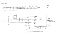
- FIG. 2 illustrates one example application of the present invention, a horizontal filter 200 for a media processor chip used to perform complex mathematical scaling calculations in implementing panoramic image zoom functionality.
- a zoom factor determines how a video picture is being scaled.
- a zoom value less than one is indicative of image compression, and a zoom value greater than one is indicative of image expansion.
- an algorithm is used to determine at precise times, whether an output pixel of the video image should be produced, the output pixel having certain characteristics.
- Video filter 200 operating in a polyphase direct filtering mode is used for either compression or expansion of video images.
- the filter continuously consumes (e.g., shifts-in, multiplies with appropriate filter equation coefficients, and accumulates) each of a sequence of input pixels from a pixel input path 210 , according to a repetitive clock cycle.
- Production of an output pixel is determined according to evaluation of a particular “condition,” the condition being evaluated through a series of computations within a functional unit datapath 220 . Evaluation of the “condition” is dependent on the mode of filtering, and whether compression or expansion of the video image is required. From evaluation of the “condition,” output pixels are periodically produced along a pixel output path 240 . “Condition” evaluation occurs each clock cycle, a clock signal being received at the filter via clock path 230 .
- Scaling operations are defined by scaling parameters, the scaling parameters defined initial scaling variable settings input to the filter from memory 120 via the input data interface 122 .
- a input pixel position pointer, “pos(n),” is updated once per input pixel to track the present location of video image processing with respect to the input image.
- expressions defining pos(n) during compression operations are as follows:
- z(n) is the zoom factor at pixel x(n).
- the present pixel position is the last pixel position modified by the present zoom factor.
- the variable pos(n) represents the pixel location of x(n) with respect to the output pixels. Pixel x(n) is located between y(floor(pos(n))) and y(ceil(pos(n))).
- pixel position pointer “pos(n),” tracks the present location of video image processing with respect to output pixel production.
- Expressions defining pos(n) use, in case of a direct polyphase filter, an inverse zoom value in determining the relationship between consumed input pixels and output pixels produced.
- the pointer variable, pos(n) is updated once per output pixel as follows:
- iz(n) is the inverse of the zoom factor at pixel y(n).
- the present pixel position is the last pixel position modified by the present inverse zoom factor.
- the variable pos(n) represents the pixel location of y(n) with respect to the input pixels. Pixel y(n) is located between x(floor(pos(n))) and x(ceil(pos(n))).
- zoom value is constant.
- a uniform compression is implemented through a constant z(n), and a uniform expansion is achieved through a constant iz(n).
- Zoom values, z(n) and iz(n) are not constant where zoom is variable.
- Panoramic zoom used only in a polyphase direct filtering mode, is implemented through a continuously-varying iz(n).
- the inverse zoom value is made variable according to a second-order polynomial in one example implementation, the polynomial coefficients being programmed into control registers.
- the “condition” which is evaluated to determine output pixel production is derived from the function pos(n).
- the function pos(n) includes an integer portion and a fractional portion in one example implementation.
- the “condition” is related to changes made to the integer portion of pos(n).
- Evaluation of the above-mentioned “condition,” dependent on the zoom value, is typically a processing speed bottleneck for scaling filter functionality, precise arithmetic over long bit widths being performed in evaluation of pos(n), and ultimately, the “condition.”
- the processing workload is even greater, and thus more costly in terms of time, where zoom value is made variable, as is the case in a panorama zoom mode for example, since the zoom variable changes continuously with each clock cycle.
- the polyphase direct filter operating in panoramic mode has input parameters, defined as follows:
- HSRC_ZOOM is the inverse of the zoom value, or iz.
- HSRC_ZOOM id a 16-bit unsigned input quantity, the most significant 4 bits represent an integer portion, and the least significant 12 bits represent a fractional portion.
- HSRC_ZOOM is specified to determine how the input image is scaled. The most significant 6 bits of the 12 bits which represent the fractional portion determine phase, and therefore, the set of filtering coefficients.
- HSRC_DZOOM is a signed 16-bit input value, and a portion of the second-order polynomial describing how the zoom continuously varies in panoramic mode.
- HSRC_DDZOOM is an unsigned 8-bit input value, and another portion of the second-order polynomial describing how the zoom continuously varies in panoramic mode.
- the “condition” is evaluated in each clock cycle, the “condition” being derived from a cascade of intermediate zoom variable calculations.
- the intermediate zoom variables are initialized at the beginning of scaling operations using the above-mentioned input parameters as follows:
- the notation used herein is the binary number variable name, followed by the most significant bit place, and the least significant bit place in square brackets separated by a colon.
- the binary variable name followed by a single squared-bracketed number, N denotes the Nth bit of the named binary variable, for example, dzoom[15] denotes the 15 th bit of the binary variable dzoom.
- the notation “ ⁇ x,y ⁇ ” denotes a concatenation operation of the first bracketed binary value, x, with the second bracketed value, y.
- the notation “8 ⁇ x ⁇ ” denotes a concatenation of eight x's, for example, 8 ⁇ 0 ⁇ denotes the binary number, 00000000.
- the variable pos[x:y] is the pixel position counter, having an integer portion and a fractional portion, bits [24:20] being the integer portion and bits [19:0] being the fractional portion.
- d zoom[15:0]( t ) d zoom[15:0]( t ⁇ 1) ⁇ 8 ⁇ 0 ⁇ , dd zoom[7:0] ⁇ ;
- zoom[23:0]( t ) zoom[23:0]( t ⁇ 1)+ ⁇ 8 ⁇ d zoom[15 ] ⁇ , d zoom[15:0] ⁇ ( t );
- pos[ 24:0]( t ) pos[ 24:0]( t ⁇ 1)+ ⁇ 0 ⁇ , zoom[23:0] ⁇ ( t );
- the variable pos[x:y] keeps track of the phase at the current position of the pixel.
- pos[x:y] includes, from most significant to least significant, one sign bit, four integer-representative bit, and the balance of the bits designating a fractional portion.
- the variable sval[4:0] determines the “condition,” equal to the value of sval[4:0], the “condition” being changes to the integer portion of pos[x:y].
- the “condition” (the value of sval[4:0]) subsequently determines the when output pixels are produced with respect to input pixels consumed.
- a circuit arrangement is configured to reduce the solution time for above-mentioned set of filtering computations in order to minimize overall computation time.
- time-dependant variable functions can be expressed for time “t” as follows:
- variable name denotes “new,” or the variable value of the present clock cycle (i.e., the variable value at time “t”), and a variable without the “n” appended denotes the variable value determined as of the previous, or last, clock cycle.
- Equation A the new binary value of dzoom 310 at time “t” (i.e., dzoomn) equals the last value of dzoom (i.e., the value at the previous, or “last,” clock cycle) 312 minus the present value of the ddzoom variable 314 concatenated with eight more significant zero bits 316 .
- the new binary value of zoom 330 at time “t” i.e., zoomn
- the last value of zoom i.e., the value at the previous, or “last,” clock cycle
- the present value of the dzoom variable 310 concatenated with eight more significant bits 334 , each having a value equal to the most significant bit of the new dzoom variable (i.e., bit number 15 of dzoomn, or dzoomn[15]). Therefore, dzoomn is concatenated with either eight preceding 1's, or eight preceding 0's.
- the new binary value of the position counter, pos(ition) 350 at time “t” (i.e., position) equals the last value of position (i.e., the value at the previous, or “last,” clock cycle) 352 minus the present value of the zoom variable 330 concatenated with a zero most significant bit 354 .
- the new binary value of the “condition” sval 370 at time “t” equals the integer portion of present value of the position variable 372 (i.e., the value at the previous, or “last,” clock cycle), bits 20-24, minus the last value of the integer portion of the position variable (i.e., position, bits 20-24) 374 .
- Equation A is evaluated using a 16-bit binary adder to compute the new value of dzoom (i.e., dzoomn).
- Computation of equation B is broken apart at the 15 th bit and separately evaluated in two portions which are subsequently concatenated..
- zoom[23:0] is alternatively expressed in equation B1 as the concatenation of bits resulting from the above-mentioned separate operations, as follows:
- Carryout, C15 is indicated in FIG. 3 at 366 is the carryout from determining the value of zoomn[15], or more completely, the carryout from determination of zoomn[15:0].
- Carryout C15 is derived, in one example implementation, from a 16-bit adder (not shown), having inputs of zoom[15:0] and dzoom[15:0]. Using the adder carryout adds to the speed of the present invention, since the adder carryout is available for further use (in a logic circuit described further below) several gate delays prior to the adder's sum being stabilized and available. Therefore, using equation B:
- zoom n[ 15:0] ⁇ zoom[15:0]+( d zoom[15:0] ⁇ 8 ⁇ 0 ⁇ , dd zoom[7:0] ⁇ )
- Equation B3 the first portion of the concatenation of equation B1 can be expressed as follows (Equation B3):
- zoom n[ 23:16] zoom[23:16]+8 ⁇ d zoom n[ 15 ] ⁇ +C 15
- Equation B4 [0068] therefore, making substitutions using equations D1-D3, equation B3 can be express as follows (Equation B4)
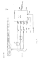
- FIG. 4 illustrates one example of a circuit arrangement 400 implementing equation B4 above.
- the upper eight bits of the new “zoom” variable are selected to be one of zoom[23:16], zoom[23:16]+1, or zoom[23:16] ⁇ 1, dependant on the respective values for C15 and dzoomn[15].
- Each of the possible selections is derived from the previous value of the “zoom” variable.
- the previous “zoom” from FIG. 3 is indicated in FIG. 4 at 332 .
- the upper eight bits of the previous “zoom” variable (i.e., zoom[23:16]) 410 is directed into a 4 ⁇ 1 (note that one-hot coding is not at all necessary and so, let us not talk about it) multiplexer (“mux”) 420 as one selectable input 412 .
- Zoom[23:16] is further directed through decrementer 430 and incrementer 440 to easily and quickly implement zoom[23:16] ⁇ 1 and zoom[23:16]+1 respectively.
- the output of incrementer 440 is zoom[23:16]+1, which is directed into mux 420 as another selectable input 414 .
- the output of decrementer 430 is zoom[23:16] ⁇ 1, which is directed into mux 420 as a third selectable input 416 as shown.
- a forth input 418 to mux 420 is not used in the present implementation.
- the sixteenth bit of the already available present dzoom i.e., dzoomn[15]
- carryout C15 is used as a second mux select 424 .
- the output 426 of mux 420 is the present value of the upper eight bits of“zoom” (i.e., zoomn[23:16]).
- the following table shows the selection logic for circuit arrangement 400 : zoomn [23:16] S 0 Input 2 S 1 (dzoomn (zoom Input 1 Input 0 (C15) [15]) [23:16]) (zoom[23:16] + 1) (zoom[23:16] ⁇ 1) 0 0 1 0 0 0 1 0 0 1 1 0 0 1 0 1 0 0 0 0 0 0 1 1 1 0 0 0 0 0 0 0 0 0 0 0 0 1 1 1 0 0 0
- Equation B a 24-bit binary addition
- the above-described method and circuit arrangement is generally applicable to addition of an N-bit binary operand and an M-bit binary operand, where N is greater than or equal to M.
- the most-significant bit of each operand is a sign bit.
- the M-bit binary operand is “extended” in length, by replicating the most significant (sign) bit until the “extended” operand has a length of N.
- the operands are split into two portions, the lesser significant M bits, and the more significant N ⁇ M bits.
- a M-bit adder is used to add the lesser significant portions.
- the carryout from the M-bit addition is used, along with the Mth bit of the original N-bit operand, is used to select, using a logic circuit (e.g., a 4 ⁇ 1 multiplexer), the most significant N ⁇ M bits as being one of:
- the incremented and decremented selections are derived via an N ⁇ M bit adder/subtracter where one operand is the N ⁇ M most significant bits of the original N-bit operand, and the other operand is 1.
- the results derived from the logic circuit are concatenated as the most significant bits to the results of the M-bit addition.
- the operands are of the same length (N); however, at least one of the operands includes, as its most-significant bits, a plurality of identical sign extension bits.
- the operands are each “split” at the same bit position into least- and most-significant portions such that an M-bit least-significant portion of one of the operands include one sign bit, and the (N ⁇ M)-bit most-significant portion of the same operand includes only the sign extension bits. Thereafter, the least- and most-significant portions are manipulated as described above.
- the method of the present specific example implementation of the invention is generally applicable where one operand can be split such that all the bits of its most-significant bits portion are all identical.
- an N-bit binary operand and an M-bit binary operand are to be added.
- the operands are unsigned binary numbers.
- the addends are split at the same bit position into least- and most-significant bit portions.
- the least-significant bit portions are added using an adder to determine a least-significant bits partial sum.
- the most-significant bit portions are processed using a logic circuit to select a most-significant bits partial sum, which is done in less time than it would take to use an adder to sum the most-significant bits portions of each addend.
- a logic circuit selects the most-significant bits partial sum responsive to selection data.
- the logic circuit selects one of a plurality of pre-determined partial sums, each of the possible selections being pre-determined from known characteristics of at least one of the addends, for example, where at least one of the most-significant bit portions of the addends is all 1's or all 0's, a set of possible selections can be predetermined as a function of the other most-significant bit portion of the other addend.
- an N-bit binary operand and an M-bit binary operand are to be added, where N ⁇ M is one.
- the operands are unsigned binary numbers.
- the M-bit binary operand is “extended” in length, prepending a zero-valued (e.g., “0”) most significant bit.
- the operands are split into two portions, the lesser significant M bits, and the more significant N ⁇ M bits.
- a M-bit adder is used to add the lesser significant portions.
- a carryout from the M-bit addition is used, along with the Mth bit of the original N-bit operand, is used to select, using a logic circuit (e.g., an XOR gate, or a multiplexer implementing an XOR function), the most significant bit as being one of the N-bit addition.
- a logic circuit e.g., an XOR gate, or a multiplexer implementing an XOR function
- an N-bit binary operand and an M-bit binary operand are to be added, where N ⁇ M is one.
- the operands are unsigned binary numbers.
- the M-bit binary operand is “extended” in length, prepending a non-zero-valued (e.g., “1”) most significant bit.
- the operands are split into two portions, the lesser significant M bits, and the more significant N ⁇ M bits.
- a M-bit adder is used to add the lesser significant portions.
- An inverted carryout from the M-bit addition is used, along with the Mth bit of the original N-bit operand, is used to select, using a logic circuit (e.g., an XOR gate, or a multiplexer implementing an XOR function), the most significant bit as being one of the N-bit addition.
- a logic circuit e.g., an XOR gate, or a multiplexer implementing an XOR function
- Equation C is expressed as follows:
- Using a 25-bit adder to repetitively compute the 25-bit position variable is expensive since 25-bit addition is typically a non-standard function.
- the operands are split into two portions, each portion being evaluated separately.
- a least-significant bits portion of each operand are added together to produce a least-significant bits partial sum using an adder having a carryout path faster than a sum path.
- a logic circuit 505 is used to select a most-significant bits partial sum, the selection being either a most-significant bits portion of one of the operands, or an offset thereof, as a function of a carryout from the adder.
- An XOR logic circuit is used in implementing equation C.
- Equation C is expressed as follows when split for evaluation at the 24-th bit:
- FIG. 3 illustrates the respective source for these selection data portions.
- the carryout, C23 is available from the 24-bit adder via an optimized carry path, approximately 2 gate delays before the sum quantity stabilizes enough for further use.
- equation D for the digital filtering example application is:
- C19 (which is not available from a standard library adder) is generated from adding single bits zoomn[19] and posn[19].
- the “condition” variable sval[4:0] is either zoomn[23:20]+1, or zoomn[23:20] dependant on the value of C19. Since zoomn[23:20] is already available, being the 4 most-significant bits of the result of equation B, selection of zoomn[23:20] or an increment thereof (pre-computed using zoomn[23:20] through an incrementer or 4-bit adder where the other operand is 1) turns on the value of intermediate carry, C19.
- Intermediate carry, C19 may not be readily available from a typical 24-bit adder that does not externally bring out intermediate carries.
- the sum's Mth bit is equal to the sum of the first operand's Mth bit, plus the second operand's Mth bit, plus any carry generated in computing the sum's lesser-significant bits.
- the carry, C19 may therefore be “reverse-engineered” from the following table used to determine the value of posn[20] for particular values of the other three variables according to equation E2:
- C19 pos[20] Zoomn[20] posn[20] 0 0 0 0 0 0 0 1 1 0 1 0 1 0 1 0 1 0 0 1 1 0 1 0 1 0 1 1 0 0 1 1 1 0 0 1 1 1 1 1 1 1 1 1 1 1 1
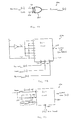
- FIG. 5B illustrates one example circuit arrangement 550 implementing of equation E3.
- An 8 ⁇ 1 mux 560 includes three select terminals. The first select terminal 562 receives pos[20], the second select terminal 564 receives zoomn[20], and the third select terminal 566 receives posn[20]. Mux inputs1, 2, 4, and 7 are tied to a logical “1,” and mux inputs 0, 3, 5, and 6 are tied to a logical “0” as shown. The mux output terminal 568 generates C19 according to the table above.
- FIG. 5C illustrates one example circuit arrangement 570 implementing selection logic responsive to C19.
- Circuit arrangement 570 includes a 2 ⁇ 1 mux 580 having a single select input terminal 582 for receiving C19 from mux 560 of FIG. 5B.
- Mux 580 selects either zoomn[23:20] directed to a first input terminal 584 , or an offset thereof (e.g., zoomn[23:20]+1) directed to a second input terminal 586 .
- the offset is derived from an incrementer 590 operating on zoomn[23:20].
- circuit arrangements 550 and 570 are combined into a single multiplexer circuit adapted to receive a first input signal being zoomn[23:20], and a second input signal being an offset of zoomn[23:20], for example zoomn[23:20]+1.
- One of the inputs are selected using the select logic of circuit arrangement 550 .
Priority Applications (8)
| Application Number | Priority Date | Filing Date | Title |
|---|---|---|---|
| US10/005,551 US20030088602A1 (en) | 2001-11-08 | 2001-11-08 | High-speed computation in arithmetic logic circuit |
| AU2002343144A AU2002343144A1 (en) | 2001-11-08 | 2002-10-30 | High-speed computation in arithmetic logic circuit |
| PCT/IB2002/004568 WO2003040859A2 (en) | 2001-11-08 | 2002-10-30 | High-speed computation in arithmetic logic circuit |
| EP02779811A EP1446713B1 (de) | 2001-11-08 | 2002-10-30 | Hochgeschwindigkeitsberechnung in einer arithmetik- und logikschaltung |
| DE60210494T DE60210494T2 (de) | 2001-11-08 | 2002-10-30 | Hochgeschwindigkeitsberechnung in einer arithmetik- und logikschaltung |
| AT02779811T ATE322715T1 (de) | 2001-11-08 | 2002-10-30 | Hochgeschwindigkeitsberechnung in einer arithmetik- und logikschaltung |
| KR10-2004-7007019A KR20040063143A (ko) | 2001-11-08 | 2002-10-30 | 오퍼랜드 가산 방법 및 회로 장치 및 컴퓨터 구현형 장치 |
| JP2003542426A JP2005508541A (ja) | 2001-11-08 | 2002-10-30 | 算術論理回路における高速演算 |
Applications Claiming Priority (1)
| Application Number | Priority Date | Filing Date | Title |
|---|---|---|---|
| US10/005,551 US20030088602A1 (en) | 2001-11-08 | 2001-11-08 | High-speed computation in arithmetic logic circuit |
Publications (1)
| Publication Number | Publication Date |
|---|---|
| US20030088602A1 true US20030088602A1 (en) | 2003-05-08 |
Family
ID=21716430
Family Applications (1)
| Application Number | Title | Priority Date | Filing Date |
|---|---|---|---|
| US10/005,551 Abandoned US20030088602A1 (en) | 2001-11-08 | 2001-11-08 | High-speed computation in arithmetic logic circuit |
Country Status (8)
| Country | Link |
|---|---|
| US (1) | US20030088602A1 (de) |
| EP (1) | EP1446713B1 (de) |
| JP (1) | JP2005508541A (de) |
| KR (1) | KR20040063143A (de) |
| AT (1) | ATE322715T1 (de) |
| AU (1) | AU2002343144A1 (de) |
| DE (1) | DE60210494T2 (de) |
| WO (1) | WO2003040859A2 (de) |
Cited By (32)
| Publication number | Priority date | Publication date | Assignee | Title |
|---|---|---|---|---|
| US20030103166A1 (en) * | 2001-11-21 | 2003-06-05 | Macinnis Alexander G. | Method and apparatus for vertical compression and de-compression of progressive video data |
| US20060179103A1 (en) * | 2005-02-09 | 2006-08-10 | International Business Machines Corporation | System and method for providing a double adder for decimal floating point operations |
| US20150178435A1 (en) * | 2013-12-19 | 2015-06-25 | Netspeed Systems | Automatic pipelining of noc channels to meet timing and/or performance |
| US9444702B1 (en) | 2015-02-06 | 2016-09-13 | Netspeed Systems | System and method for visualization of NoC performance based on simulation output |
| US9568970B1 (en) | 2015-02-12 | 2017-02-14 | Netspeed Systems, Inc. | Hardware and software enabled implementation of power profile management instructions in system on chip |
| US9590813B1 (en) | 2013-08-07 | 2017-03-07 | Netspeed Systems | Supporting multicast in NoC interconnect |
| US9742630B2 (en) | 2014-09-22 | 2017-08-22 | Netspeed Systems | Configurable router for a network on chip (NoC) |
| US9769077B2 (en) | 2014-02-20 | 2017-09-19 | Netspeed Systems | QoS in a system with end-to-end flow control and QoS aware buffer allocation |
| US9825887B2 (en) | 2015-02-03 | 2017-11-21 | Netspeed Systems | Automatic buffer sizing for optimal network-on-chip design |
| US9825809B2 (en) | 2015-05-29 | 2017-11-21 | Netspeed Systems | Dynamically configuring store-and-forward channels and cut-through channels in a network-on-chip |
| US9864728B2 (en) | 2015-05-29 | 2018-01-09 | Netspeed Systems, Inc. | Automatic generation of physically aware aggregation/distribution networks |
| US9928204B2 (en) | 2015-02-12 | 2018-03-27 | Netspeed Systems, Inc. | Transaction expansion for NoC simulation and NoC design |
| US10050843B2 (en) | 2015-02-18 | 2018-08-14 | Netspeed Systems | Generation of network-on-chip layout based on user specified topological constraints |
| US10063496B2 (en) | 2017-01-10 | 2018-08-28 | Netspeed Systems Inc. | Buffer sizing of a NoC through machine learning |
| US10074053B2 (en) | 2014-10-01 | 2018-09-11 | Netspeed Systems | Clock gating for system-on-chip elements |
| US10084725B2 (en) | 2017-01-11 | 2018-09-25 | Netspeed Systems, Inc. | Extracting features from a NoC for machine learning construction |
| US10084692B2 (en) | 2013-12-30 | 2018-09-25 | Netspeed Systems, Inc. | Streaming bridge design with host interfaces and network on chip (NoC) layers |
| US10218580B2 (en) | 2015-06-18 | 2019-02-26 | Netspeed Systems | Generating physically aware network-on-chip design from a physical system-on-chip specification |
| US10298485B2 (en) | 2017-02-06 | 2019-05-21 | Netspeed Systems, Inc. | Systems and methods for NoC construction |
| US10313269B2 (en) | 2016-12-26 | 2019-06-04 | Netspeed Systems, Inc. | System and method for network on chip construction through machine learning |
| US10348563B2 (en) | 2015-02-18 | 2019-07-09 | Netspeed Systems, Inc. | System-on-chip (SoC) optimization through transformation and generation of a network-on-chip (NoC) topology |
| US10355996B2 (en) | 2012-10-09 | 2019-07-16 | Netspeed Systems | Heterogeneous channel capacities in an interconnect |
| US10419300B2 (en) | 2017-02-01 | 2019-09-17 | Netspeed Systems, Inc. | Cost management against requirements for the generation of a NoC |
| US10452124B2 (en) | 2016-09-12 | 2019-10-22 | Netspeed Systems, Inc. | Systems and methods for facilitating low power on a network-on-chip |
| US10496770B2 (en) | 2013-07-25 | 2019-12-03 | Netspeed Systems | System level simulation in Network on Chip architecture |
| US10547514B2 (en) | 2018-02-22 | 2020-01-28 | Netspeed Systems, Inc. | Automatic crossbar generation and router connections for network-on-chip (NOC) topology generation |
| US10735335B2 (en) | 2016-12-02 | 2020-08-04 | Netspeed Systems, Inc. | Interface virtualization and fast path for network on chip |
| US10896476B2 (en) | 2018-02-22 | 2021-01-19 | Netspeed Systems, Inc. | Repository of integration description of hardware intellectual property for NoC construction and SoC integration |
| US10983910B2 (en) | 2018-02-22 | 2021-04-20 | Netspeed Systems, Inc. | Bandwidth weighting mechanism based network-on-chip (NoC) configuration |
| US11023377B2 (en) | 2018-02-23 | 2021-06-01 | Netspeed Systems, Inc. | Application mapping on hardened network-on-chip (NoC) of field-programmable gate array (FPGA) |
| US11144457B2 (en) | 2018-02-22 | 2021-10-12 | Netspeed Systems, Inc. | Enhanced page locality in network-on-chip (NoC) architectures |
| US11176302B2 (en) | 2018-02-23 | 2021-11-16 | Netspeed Systems, Inc. | System on chip (SoC) builder |
Citations (3)
| Publication number | Priority date | Publication date | Assignee | Title |
|---|---|---|---|---|
| US5418736A (en) * | 1994-03-11 | 1995-05-23 | Nexgen, Inc. | Optimized binary adders and comparators for inputs having different widths |
| US6065034A (en) * | 1998-04-08 | 2000-05-16 | Advanced Micro Devices, Inc. | Circuit and method employing an adder for sign extending operands |
| US6260055B1 (en) * | 1997-10-15 | 2001-07-10 | Kabushiki Kaisha Toshiba | Data split parallel shifter and parallel adder/subtractor |
Family Cites Families (4)
| Publication number | Priority date | Publication date | Assignee | Title |
|---|---|---|---|---|
| US4203157A (en) * | 1978-09-05 | 1980-05-13 | Motorola, Inc. | Carry anticipator circuit and method |
| BR8602717A (pt) * | 1985-09-11 | 1987-04-14 | Sperry Corp | Aparelho para efetuar adicao de binarios |
| US5504698A (en) * | 1994-05-17 | 1996-04-02 | Silicon Graphics, Inc. | Compact dual function adder |
| EP0955576B1 (de) * | 1998-05-08 | 2003-08-13 | STMicroelectronics S.r.l. | Digitaler Hochgeschwindigkeits-Akkumulator mit grossem Dynamikbereich |
-
2001
- 2001-11-08 US US10/005,551 patent/US20030088602A1/en not_active Abandoned
-
2002
- 2002-10-30 DE DE60210494T patent/DE60210494T2/de not_active Expired - Fee Related
- 2002-10-30 KR KR10-2004-7007019A patent/KR20040063143A/ko not_active Application Discontinuation
- 2002-10-30 EP EP02779811A patent/EP1446713B1/de not_active Expired - Lifetime
- 2002-10-30 AU AU2002343144A patent/AU2002343144A1/en not_active Abandoned
- 2002-10-30 JP JP2003542426A patent/JP2005508541A/ja active Pending
- 2002-10-30 AT AT02779811T patent/ATE322715T1/de not_active IP Right Cessation
- 2002-10-30 WO PCT/IB2002/004568 patent/WO2003040859A2/en active IP Right Grant
Patent Citations (3)
| Publication number | Priority date | Publication date | Assignee | Title |
|---|---|---|---|---|
| US5418736A (en) * | 1994-03-11 | 1995-05-23 | Nexgen, Inc. | Optimized binary adders and comparators for inputs having different widths |
| US6260055B1 (en) * | 1997-10-15 | 2001-07-10 | Kabushiki Kaisha Toshiba | Data split parallel shifter and parallel adder/subtractor |
| US6065034A (en) * | 1998-04-08 | 2000-05-16 | Advanced Micro Devices, Inc. | Circuit and method employing an adder for sign extending operands |
Cited By (47)
| Publication number | Priority date | Publication date | Assignee | Title |
|---|---|---|---|---|
| US20030103166A1 (en) * | 2001-11-21 | 2003-06-05 | Macinnis Alexander G. | Method and apparatus for vertical compression and de-compression of progressive video data |
| US20060179103A1 (en) * | 2005-02-09 | 2006-08-10 | International Business Machines Corporation | System and method for providing a double adder for decimal floating point operations |
| US7475104B2 (en) * | 2005-02-09 | 2009-01-06 | International Business Machines Corporation | System and method for providing a double adder for decimal floating point operations |
| US20090112960A1 (en) * | 2005-02-09 | 2009-04-30 | International Business Machines Corporation | System and Method for Providing a Double Adder for Decimal Floating Point Operations |
| US8219604B2 (en) | 2005-02-09 | 2012-07-10 | International Business Machines Corporation | System and method for providing a double adder for decimal floating point operations |
| US10355996B2 (en) | 2012-10-09 | 2019-07-16 | Netspeed Systems | Heterogeneous channel capacities in an interconnect |
| US10496770B2 (en) | 2013-07-25 | 2019-12-03 | Netspeed Systems | System level simulation in Network on Chip architecture |
| US9590813B1 (en) | 2013-08-07 | 2017-03-07 | Netspeed Systems | Supporting multicast in NoC interconnect |
| US20150178435A1 (en) * | 2013-12-19 | 2015-06-25 | Netspeed Systems | Automatic pipelining of noc channels to meet timing and/or performance |
| US9158882B2 (en) * | 2013-12-19 | 2015-10-13 | Netspeed Systems | Automatic pipelining of NoC channels to meet timing and/or performance |
| US10084692B2 (en) | 2013-12-30 | 2018-09-25 | Netspeed Systems, Inc. | Streaming bridge design with host interfaces and network on chip (NoC) layers |
| US9769077B2 (en) | 2014-02-20 | 2017-09-19 | Netspeed Systems | QoS in a system with end-to-end flow control and QoS aware buffer allocation |
| US10110499B2 (en) | 2014-02-20 | 2018-10-23 | Netspeed Systems | QoS in a system with end-to-end flow control and QoS aware buffer allocation |
| US9742630B2 (en) | 2014-09-22 | 2017-08-22 | Netspeed Systems | Configurable router for a network on chip (NoC) |
| US10074053B2 (en) | 2014-10-01 | 2018-09-11 | Netspeed Systems | Clock gating for system-on-chip elements |
| US9860197B2 (en) | 2015-02-03 | 2018-01-02 | Netspeed Systems, Inc. | Automatic buffer sizing for optimal network-on-chip design |
| US9825887B2 (en) | 2015-02-03 | 2017-11-21 | Netspeed Systems | Automatic buffer sizing for optimal network-on-chip design |
| US9444702B1 (en) | 2015-02-06 | 2016-09-13 | Netspeed Systems | System and method for visualization of NoC performance based on simulation output |
| US9829962B2 (en) | 2015-02-12 | 2017-11-28 | Netspeed Systems, Inc. | Hardware and software enabled implementation of power profile management instructions in system on chip |
| US9568970B1 (en) | 2015-02-12 | 2017-02-14 | Netspeed Systems, Inc. | Hardware and software enabled implementation of power profile management instructions in system on chip |
| US9928204B2 (en) | 2015-02-12 | 2018-03-27 | Netspeed Systems, Inc. | Transaction expansion for NoC simulation and NoC design |
| US10348563B2 (en) | 2015-02-18 | 2019-07-09 | Netspeed Systems, Inc. | System-on-chip (SoC) optimization through transformation and generation of a network-on-chip (NoC) topology |
| US10218581B2 (en) | 2015-02-18 | 2019-02-26 | Netspeed Systems | Generation of network-on-chip layout based on user specified topological constraints |
| US10050843B2 (en) | 2015-02-18 | 2018-08-14 | Netspeed Systems | Generation of network-on-chip layout based on user specified topological constraints |
| US9825809B2 (en) | 2015-05-29 | 2017-11-21 | Netspeed Systems | Dynamically configuring store-and-forward channels and cut-through channels in a network-on-chip |
| US9864728B2 (en) | 2015-05-29 | 2018-01-09 | Netspeed Systems, Inc. | Automatic generation of physically aware aggregation/distribution networks |
| US10218580B2 (en) | 2015-06-18 | 2019-02-26 | Netspeed Systems | Generating physically aware network-on-chip design from a physical system-on-chip specification |
| US10564703B2 (en) | 2016-09-12 | 2020-02-18 | Netspeed Systems, Inc. | Systems and methods for facilitating low power on a network-on-chip |
| US10452124B2 (en) | 2016-09-12 | 2019-10-22 | Netspeed Systems, Inc. | Systems and methods for facilitating low power on a network-on-chip |
| US10613616B2 (en) | 2016-09-12 | 2020-04-07 | Netspeed Systems, Inc. | Systems and methods for facilitating low power on a network-on-chip |
| US10564704B2 (en) | 2016-09-12 | 2020-02-18 | Netspeed Systems, Inc. | Systems and methods for facilitating low power on a network-on-chip |
| US10749811B2 (en) | 2016-12-02 | 2020-08-18 | Netspeed Systems, Inc. | Interface virtualization and fast path for Network on Chip |
| US10735335B2 (en) | 2016-12-02 | 2020-08-04 | Netspeed Systems, Inc. | Interface virtualization and fast path for network on chip |
| US10313269B2 (en) | 2016-12-26 | 2019-06-04 | Netspeed Systems, Inc. | System and method for network on chip construction through machine learning |
| US10063496B2 (en) | 2017-01-10 | 2018-08-28 | Netspeed Systems Inc. | Buffer sizing of a NoC through machine learning |
| US10523599B2 (en) | 2017-01-10 | 2019-12-31 | Netspeed Systems, Inc. | Buffer sizing of a NoC through machine learning |
| US10084725B2 (en) | 2017-01-11 | 2018-09-25 | Netspeed Systems, Inc. | Extracting features from a NoC for machine learning construction |
| US10419300B2 (en) | 2017-02-01 | 2019-09-17 | Netspeed Systems, Inc. | Cost management against requirements for the generation of a NoC |
| US10469338B2 (en) | 2017-02-01 | 2019-11-05 | Netspeed Systems, Inc. | Cost management against requirements for the generation of a NoC |
| US10469337B2 (en) | 2017-02-01 | 2019-11-05 | Netspeed Systems, Inc. | Cost management against requirements for the generation of a NoC |
| US10298485B2 (en) | 2017-02-06 | 2019-05-21 | Netspeed Systems, Inc. | Systems and methods for NoC construction |
| US10547514B2 (en) | 2018-02-22 | 2020-01-28 | Netspeed Systems, Inc. | Automatic crossbar generation and router connections for network-on-chip (NOC) topology generation |
| US10896476B2 (en) | 2018-02-22 | 2021-01-19 | Netspeed Systems, Inc. | Repository of integration description of hardware intellectual property for NoC construction and SoC integration |
| US10983910B2 (en) | 2018-02-22 | 2021-04-20 | Netspeed Systems, Inc. | Bandwidth weighting mechanism based network-on-chip (NoC) configuration |
| US11144457B2 (en) | 2018-02-22 | 2021-10-12 | Netspeed Systems, Inc. | Enhanced page locality in network-on-chip (NoC) architectures |
| US11176302B2 (en) | 2018-02-23 | 2021-11-16 | Netspeed Systems, Inc. | System on chip (SoC) builder |
| US11023377B2 (en) | 2018-02-23 | 2021-06-01 | Netspeed Systems, Inc. | Application mapping on hardened network-on-chip (NoC) of field-programmable gate array (FPGA) |
Also Published As
| Publication number | Publication date |
|---|---|
| EP1446713A2 (de) | 2004-08-18 |
| ATE322715T1 (de) | 2006-04-15 |
| WO2003040859A2 (en) | 2003-05-15 |
| EP1446713B1 (de) | 2006-04-05 |
| KR20040063143A (ko) | 2004-07-12 |
| DE60210494D1 (de) | 2006-05-18 |
| DE60210494T2 (de) | 2006-11-30 |
| WO2003040859A3 (en) | 2003-11-27 |
| JP2005508541A (ja) | 2005-03-31 |
| AU2002343144A1 (en) | 2003-05-19 |
Similar Documents
| Publication | Publication Date | Title |
|---|---|---|
| EP1446713B1 (de) | Hochgeschwindigkeitsberechnung in einer arithmetik- und logikschaltung | |
| US5644522A (en) | Method, apparatus and system for multiply rounding using redundant coded multiply result | |
| EP0657803B1 (de) | Arithmetik-Logikschaltung mit drei Eingängen | |
| US5961635A (en) | Three input arithmetic logic unit with barrel rotator and mask generator | |
| US5600847A (en) | Three input arithmetic logic unit with mask generator | |
| USRE44190E1 (en) | Long instruction word controlling plural independent processor operations | |
| US5696959A (en) | Memory store from a selected one of a register pair conditional upon the state of a selected status bit | |
| US6116768A (en) | Three input arithmetic logic unit with barrel rotator | |
| US5442577A (en) | Sign-extension of immediate constants in an alu | |
| US6098163A (en) | Three input arithmetic logic unit with shifter | |
| US6016538A (en) | Method, apparatus and system forming the sum of data in plural equal sections of a single data word | |
| EP0656582B1 (de) | Schaltung und Verfahren zur parallelen Addition und Mittelwertbildung | |
| EP0657802B1 (de) | Rotationsregister zur orthogonalen Datentransformation | |
| JPH087084A (ja) | 第1、第2及び第3の入力の第1のブール組合せプラス第1、第2及び第3の入力の第2のブール組合せの和を形成する3入力算術論理装置 | |
| JPH07287567A (ja) | 複数の独立区分と各区分からの結果を記憶するレジスタとを有する算術論理装置 | |
| JPH087083A (ja) | 算術及び論理混合組合せを形成する3入力算術論理装置 | |
| US6026484A (en) | Data processing apparatus, system and method for if, then, else operation using write priority | |
| US5712999A (en) | Address generator employing selective merge of two independent addresses | |
| US5442581A (en) | Iterative division apparatus, system and method forming plural quotient bits per iteration | |
| US5479166A (en) | Huffman decoding method, circuit and system employing conditional subtraction for conversion of negative numbers | |
| US5512896A (en) | Huffman encoding method, circuit and system employing most significant bit change for size detection | |
| US5689695A (en) | Conditional processor operation based upon result of two consecutive prior processor operations | |
| EP0660223B1 (de) | Drei-Eingänge-Arithmetik-Logik-Einheit mit Trommel-Rotationsschaltung | |
| JP2003084972A (ja) | 条件付減算命令の実行速度を改善し、命令が正しく実行されるオペランドの範囲を拡大する方法 | |
| JP2005259083A (ja) | ディジタル回路 |
Legal Events
| Date | Code | Title | Description |
|---|---|---|---|
| AS | Assignment |
Owner name: KONINKLIJKE PHILIPS ELECTRONICS N.V., NETHERLANDS Free format text: ASSIGNMENT OF ASSIGNORS INTEREST;ASSIGNORS:DUTTA, SANTANU;SINGH, DEEPAK K.;REEL/FRAME:012359/0577 Effective date: 20011105 |
|
| AS | Assignment |
Owner name: NXP B.V., NETHERLANDS Free format text: ASSIGNMENT OF ASSIGNORS INTEREST;ASSIGNOR:KONINKLIJKE PHILIPS ELECTRONICS N.V.;REEL/FRAME:019719/0843 Effective date: 20070704 Owner name: NXP B.V.,NETHERLANDS Free format text: ASSIGNMENT OF ASSIGNORS INTEREST;ASSIGNOR:KONINKLIJKE PHILIPS ELECTRONICS N.V.;REEL/FRAME:019719/0843 Effective date: 20070704 |
|
| STCB | Information on status: application discontinuation |
Free format text: ABANDONED -- FAILURE TO PAY ISSUE FEE |