US12349574B2 - Display panel, manufacturing method thereof, and display device - Google Patents
Display panel, manufacturing method thereof, and display device Download PDFInfo
- Publication number
- US12349574B2 US12349574B2 US17/764,185 US202117764185A US12349574B2 US 12349574 B2 US12349574 B2 US 12349574B2 US 202117764185 A US202117764185 A US 202117764185A US 12349574 B2 US12349574 B2 US 12349574B2
- Authority
- US
- United States
- Prior art keywords
- pixel
- sub
- inhibition layer
- display panel
- pixels
- Prior art date
- Legal status (The legal status is an assumption and is not a legal conclusion. Google has not performed a legal analysis and makes no representation as to the accuracy of the status listed.)
- Active, expires
Links
Images


Classifications
-
- H—ELECTRICITY
- H10—SEMICONDUCTOR DEVICES; ELECTRIC SOLID-STATE DEVICES NOT OTHERWISE PROVIDED FOR
- H10K—ORGANIC ELECTRIC SOLID-STATE DEVICES
- H10K59/00—Integrated devices, or assemblies of multiple devices, comprising at least one organic light-emitting element covered by group H10K50/00
- H10K59/10—OLED displays
- H10K59/12—Active-matrix OLED [AMOLED] displays
- H10K59/1201—Manufacture or treatment
-
- H—ELECTRICITY
- H10—SEMICONDUCTOR DEVICES; ELECTRIC SOLID-STATE DEVICES NOT OTHERWISE PROVIDED FOR
- H10K—ORGANIC ELECTRIC SOLID-STATE DEVICES
- H10K59/00—Integrated devices, or assemblies of multiple devices, comprising at least one organic light-emitting element covered by group H10K50/00
- H10K59/10—OLED displays
- H10K59/17—Passive-matrix OLED displays
- H10K59/173—Passive-matrix OLED displays comprising banks or shadow masks
-
- H—ELECTRICITY
- H10—SEMICONDUCTOR DEVICES; ELECTRIC SOLID-STATE DEVICES NOT OTHERWISE PROVIDED FOR
- H10K—ORGANIC ELECTRIC SOLID-STATE DEVICES
- H10K59/00—Integrated devices, or assemblies of multiple devices, comprising at least one organic light-emitting element covered by group H10K50/00
- H10K59/30—Devices specially adapted for multicolour light emission
- H10K59/35—Devices specially adapted for multicolour light emission comprising red-green-blue [RGB] subpixels
- H10K59/353—Devices specially adapted for multicolour light emission comprising red-green-blue [RGB] subpixels characterised by the geometrical arrangement of the RGB subpixels
-
- H—ELECTRICITY
- H10—SEMICONDUCTOR DEVICES; ELECTRIC SOLID-STATE DEVICES NOT OTHERWISE PROVIDED FOR
- H10K—ORGANIC ELECTRIC SOLID-STATE DEVICES
- H10K59/00—Integrated devices, or assemblies of multiple devices, comprising at least one organic light-emitting element covered by group H10K50/00
- H10K59/80—Constructional details
- H10K59/805—Electrodes
- H10K59/8052—Cathodes
- H10K59/80521—Cathodes characterised by their shape
-
- H—ELECTRICITY
- H10—SEMICONDUCTOR DEVICES; ELECTRIC SOLID-STATE DEVICES NOT OTHERWISE PROVIDED FOR
- H10K—ORGANIC ELECTRIC SOLID-STATE DEVICES
- H10K71/00—Manufacture or treatment specially adapted for the organic devices covered by this subclass
Definitions
- a display panel including: a substrate, and a plurality of pixel units on the substrate.
- the plurality of pixel units are arranged in an array, and two adjacent columns of the pixel units are spaced apart from each other to form an interval area.
- Each pixel unit includes a pixel defining layer and sub-pixels, and the sub-pixels are in pixel areas defined by the pixel defining layer. Cathodes of all sub-pixels in one column of pixel units are connected as one single piece.
- the transparent inhibition layer adopts any one of 8-hydroxyquinoline-lithium, 8-hydroxyquinoline aluminum salt, and lithium fluoride.
- the sub-pixels in each pixel unit include a first sub-pixel, a second sub-pixel and a third sub-pixel.
- a shape of each sub-pixels is a regular hexagon.
- the first sub-pixel and the second sub-pixel are arranged along the column direction of the array, and along the column direction of the array, the third sub-pixel in each pixel unit is located on a same side of the straight line on which the first sub-pixel and the second sub-pixel in the pixel unit including the third sub-pixel are arranged.
- the first sub-pixel, the second sub-pixel and the third sub-pixel are spaced apart from each other, and the third sub-pixel corresponds to an interval between the first sub-pixel and the second sub-pixel.
- colors of the first sub-pixel, the second sub-pixel and the third sub-pixel are different.
- the color of the second sub-pixel is any one of red, green and blue.
- the color of the third sub-pixel is any one of red, green and blue.
- the embodiments of the present disclosure further provide a display device including the display panel as described above.
- patterns of the transparent inhibition layer on the first mask plate and the second mask plate are the same, and the partial transparent inhibition layer pattern on the first mask plate and the another partial transparent inhibition layer pattern on the second mask plate are partially overlapped.
- FIG. 1 is a top view of a structure of a display panel according to an embodiment of the present disclosure
- FIG. 2 is a cross-sectional view of a structure of the display panel in FIG. 1 along a section line AA;
- FIG. 3 is a top view of an arrangement of sub-pixels in the display panel in FIG. 1 ;
- FIG. 5 is a schematic diagram of a process of forming a pattern of a transparent inhibition layer by evaporation using the mask plate in FIG. 4 ;
- FIG. 6 is a schematic diagram illustrating evaporation effect of patterns of transparent inhibition layers and cathodes of a display panel according to an embodiment of the present disclosure
- FIG. 8 is a top view of a structure of another display panel according to an embodiment of the present disclosure.
- FIG. 11 is a top view of a structure of a mask plate having a partial transparent inhibition layer pattern according to another embodiment of the present disclosure.
- FIG. 12 is a schematic diagram of a process of forming a pattern of a transparent inhibition layer by evaporation using the mask plate in FIG. 11 ;
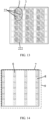
- FIG. 13 is a schematic diagram illustrating evaporation effect of patterns of transparent inhibition layers and cathodes of another display panel according to an embodiment of the present disclosure.
- FIG. 14 is a schematic diagram of a process of forming a pattern of a transparent inhibition layer by evaporation using a first mask plate and a second mask plate according to another embodiment of the present disclosure.
- the manufacturing method of the display panel includes: sequentially forming the anode, the pixel defining layer, and the light-emitting functional layer on the substrate.
- the anode, the pixel defining layer, and the light-emitting functional layer are all formed by existing processes, which are not described repeatedly herein.
- the material of the transparent inhibition layer can prevent the material of the cathode from forming a film.
- the material of the transparent inhibition layer in the interval area, it can be ensured that the material of the cathode will not form a film in the interval area, and at the same time, it can also be ensured that the material of the cathode can completely cover actual pixel light-emitting areas, so as to ensure that the cathodes of adjacent columns of pixel units are independent of each other, thereby ensuring normal display of the display panel.
- a process for manufacturing the transparent inhibition layer is simple, and difficulty in implementing the process is low.
- forming the transparent inhibition layer includes the following steps S 101 and S 102 .
- step S 101 a mask plate 5 with a partial transparent inhibition layer pattern 4 is adopted to form a pattern of one part of the transparent inhibition layer by evaporation.
- step S 102 the mask plate 5 with the partial transparent inhibition layer pattern 4 is moved and adopted to form a pattern of the other part of the transparent inhibition layer by evaporation.
- forming the cathodes 222 includes: forming a pattern of the cathodes 222 by evaporation using a mask plate having a first pattern.
- the first pattern is an overall pattern of areas where the pixel units are located and the interval areas on the substrate. That is, the first pattern corresponds to the display area of the entire display panel.
- the material of the cathodes cannot form a film in the area of the pattern of the transparent inhibition layer 3 , thereby forming patterns of the cathodes 222 which are independent of each other.
- the step of forming the transparent inhibition layer may also include steps S 101 ′ and S 102 ′ as shown in FIG. 7 .
- step S 101 ′ a first mask 7 with a partial transparent inhibition layer pattern 6 and a second mask 9 with another partial transparent inhibition layer pattern 8 are spliced together such that the partial transparent inhibition layer pattern 6 and another part partial transparent inhibition layer pattern 8 are spliced together to form a pattern of the complete transparent inhibition layer.
- step S 102 ′ the pattern of the transparent inhibition layer is formed by evaporation.
- the partial transparent inhibition layer pattern on the first mask plate 7 and the another partial transparent inhibition layer pattern on the second mask plate 9 are the same, and the partial transparent inhibition layer pattern 6 on the first mask 7 and another partial transparent inhibition layer pattern 8 on the second mask 9 are partially overlapped. In this way, the pattern of the complete transparent inhibition layer can be formed by seamless splicing, so that the pattern of the transparent inhibition layer can be formed by one evaporation.
- the process for forming the transparent inhibiting layer is simple, and the difficulty in implementing the process is low.
- Embodiments of the present disclosure also provide a display panel. As shown in FIGS. 8 to 10 , it is different from the above-described embodiments that the sub-pixels 22 are in the shape of a rectangle; the first sub-pixels 201 and the second sub-pixels 202 are arranged along the column direction Y of the array, and the third sub-pixel 203 in each pixel unit 2 is located, along the column direction Y of the array, on a same side of the straight line on which the first sub-pixel 201 and the second sub-pixel 202 in the pixel unit 2 including the third sub-pixel 203 are arranged.
- the shape and arrangement of the sub-pixels can effectively increase the area of the interval area under the condition that the area of the display area of the display panel is fixed, so that transmittance of light for the under-screen identification device can be improved, and the requirements of the under-screen identification device for the light transmittance of the display panel can be better met.
- the embodiments also provide a manufacturing method of the display panel. As shown in FIGS. 11 to 14 , the manufacturing method of the display panel in this embodiment is the same as that in the above-described embodiments, and is not repeated here.
- the transparent inhibition layer adopts a transparent inorganic inhibitor material or a transparent organic inhibitor material
- the cathode adopts magnesium or modified magnesium. Since the material of the transparent inhibition layer and the material of the cathode are mutually exclusive, the material of the transparent inhibition layer can prevent the material of the cathode from forming a film.
- the material of the transparent inhibition layer By forming the material of the transparent inhibition layer in the interval area, it can be ensured that the material of the cathode will not form a film in the interval area, and at the same time, it can also be ensured that the material of the cathode can completely cover actual pixel light-emitting areas, so as to ensure that the cathodes of pixel units in adjacent columns are independent of each other, thereby ensuring that the display panel can display normally. Because the material of the transparent inhibition layer has good light transmittance, light transmittance of the display panel can be greatly improved, so that light transmittance for the under-screen identification device of the display panel can be greatly improved, thereby meeting the requirements of the under-screen identification device for the light transmittance of the display panel. In addition, compared with the current technique of adopting the separation spacers, the process for manufacturing the transparent inhibition layer is simple, and difficulty in implementing the process is low.
- An embodiment of the present disclosure further provides a display device, including the display panel in any one of the above-described embodiments.
- the light transmittance of the display device can be improved while ensuring normal display of the display device, so that the requirements of the under-screen identification device for the light transmittance of the display device can be met.
- the display device has a simple manufacturing process and low process difficulty.
- the display device provided by exemplary embodiments of the present disclosure may be any product or component with a display function, such as an OLED panel, an OLED TV, a display, a mobile phone, or a navigator.
- a display function such as an OLED panel, an OLED TV, a display, a mobile phone, or a navigator.
Landscapes
- Engineering & Computer Science (AREA)
- Manufacturing & Machinery (AREA)
- Microelectronics & Electronic Packaging (AREA)
- Electroluminescent Light Sources (AREA)
Abstract
Description
-
- forming the plurality of pixel units includes forming a pixel defining layer and sub-pixels, the sub-pixels being formed in pixel areas defined by the pixel defining layer; and cathodes of all sub-pixels in one column of pixel units being formed as one single piece;
- after forming the pixel defining layer and before forming cathodes, the manufacturing method of the display panel further includes forming a transparent inhibition layer, the transparent inhibition layer is formed in the interval area, and an orthographic projection of the transparent inhibition layer on the substrate completely covers the interval area.
-
- moving the mask plate having the partial transparent inhibition layer pattern, and forming a pattern of the other part of the transparent inhibition layer by evaporation.
-
- forming the pattern of the transparent inhibition layer by evaporation.
-
- wherein the first pattern is an overall pattern of areas where all pixel units are located and all interval areas on the substrate.
-
- 1, substrate; 2, pixel unit; 21, pixel defining layer; 22, sub-pixel; 220, anode; 221, light-emitting functional layer; 222, cathode; 3, transparent inhibition layer; 201, first sub-pixel; 202, second sub-pixel; 203, third sub-pixel; 4, partial transparent inhibition layer pattern; 5, mask plate; 6, partial transparent inhibition layer pattern; 7, first mask plate; 8, another partial transparent inhibition layer pattern; 9, second mask plate.
Claims (20)
Applications Claiming Priority (3)
| Application Number | Priority Date | Filing Date | Title |
|---|---|---|---|
| CN202010575778.0A CN111682120B (en) | 2020-06-22 | 2020-06-22 | Display panel, manufacturing method thereof, and display device |
| CN202010575778.0 | 2020-06-22 | ||
| PCT/CN2021/093339 WO2021258886A1 (en) | 2020-06-22 | 2021-05-12 | Display panel and preparation method therefor, and display apparatus |
Publications (2)
| Publication Number | Publication Date |
|---|---|
| US20220352299A1 US20220352299A1 (en) | 2022-11-03 |
| US12349574B2 true US12349574B2 (en) | 2025-07-01 |
Family
ID=72456094
Family Applications (1)
| Application Number | Title | Priority Date | Filing Date |
|---|---|---|---|
| US17/764,185 Active 2042-11-04 US12349574B2 (en) | 2020-06-22 | 2021-05-12 | Display panel, manufacturing method thereof, and display device |
Country Status (3)
| Country | Link |
|---|---|
| US (1) | US12349574B2 (en) |
| CN (1) | CN111682120B (en) |
| WO (1) | WO2021258886A1 (en) |
Families Citing this family (22)
| Publication number | Priority date | Publication date | Assignee | Title |
|---|---|---|---|---|
| US10270033B2 (en) | 2015-10-26 | 2019-04-23 | Oti Lumionics Inc. | Method for patterning a coating on a surface and device including a patterned coating |
| CN110301053B (en) | 2016-12-02 | 2024-05-10 | Oti照明公司 | Device comprising a conductive coating disposed over an emission region and method thereof |
| CN116583131A (en) | 2017-04-26 | 2023-08-11 | Oti照明公司 | Method for patterning a coating on a surface and apparatus comprising the patterned coating |
| JP7264488B2 (en) | 2017-05-17 | 2023-04-25 | オーティーアイ ルミオニクス インコーポレーテッド | Methods and devices containing conductive coatings for selectively depositing conductive coatings over patterned coatings |
| US11751415B2 (en) | 2018-02-02 | 2023-09-05 | Oti Lumionics Inc. | Materials for forming a nucleation-inhibiting coating and devices incorporating same |
| JP2022508040A (en) | 2018-11-23 | 2022-01-19 | オーティーアイ ルミオニクス インコーポレーテッド | Optoelectronic device containing light transmission region |
| JP7390739B2 (en) | 2019-03-07 | 2023-12-04 | オーティーアイ ルミオニクス インコーポレーテッド | Materials for forming nucleation-inhibiting coatings and devices incorporating the same |
| KR102831863B1 (en) | 2019-04-18 | 2025-07-10 | 오티아이 루미오닉스 인크. | Material for forming a nucleation-inhibiting coating and device comprising the same |
| JP7576337B2 (en) | 2019-05-08 | 2024-11-01 | オーティーアイ ルミオニクス インコーポレーテッド | Materials for forming nucleation-inhibiting coatings and devices incorporating same - Patents.com |
| CN114097102B (en) | 2019-06-26 | 2023-11-03 | Oti照明公司 | Optoelectronic device comprising a light transmissive region having light diffraction features |
| US11832473B2 (en) | 2019-06-26 | 2023-11-28 | Oti Lumionics Inc. | Optoelectronic device including light transmissive regions, with light diffraction characteristics |
| KR20260036028A (en) | 2019-12-24 | 2026-03-13 | 오티아이 루미오닉스 인크. | A light emitting device including a capping layer and a method for manufacturing the same |
| CN111682120B (en) | 2020-06-22 | 2023-09-05 | 京东方科技集团股份有限公司 | Display panel, manufacturing method thereof, and display device |
| US12113279B2 (en) | 2020-09-22 | 2024-10-08 | Oti Lumionics Inc. | Device incorporating an IR signal transmissive region |
| WO2022123431A1 (en) | 2020-12-07 | 2022-06-16 | Oti Lumionics Inc. | Patterning a conductive deposited layer using a nucleation inhibiting coating and an underlying metallic coating |
| CN113054134B (en) * | 2021-03-09 | 2022-06-10 | 武汉华星光电半导体显示技术有限公司 | Display panel |
| CN113054133B (en) * | 2021-03-09 | 2022-09-16 | 武汉华星光电半导体显示技术有限公司 | Display panel and preparation method thereof |
| WO2022222111A1 (en) * | 2021-04-22 | 2022-10-27 | 京东方科技集团股份有限公司 | Display substrate, display apparatus, and manufacturing method |
| CN114438457A (en) * | 2021-12-27 | 2022-05-06 | 长沙惠科光电有限公司 | Mask plate structure, OLED display panel, manufacturing method of OLED display panel and display device |
| CN114442359A (en) * | 2022-01-21 | 2022-05-06 | 惠州Tcl移动通信有限公司 | Pixel arrangement structure and display device |
| CN114497415B (en) * | 2022-01-24 | 2024-03-19 | 京东方科技集团股份有限公司 | Display panel, manufacturing method and display device thereof |
| CN115867067A (en) * | 2022-11-30 | 2023-03-28 | 京东方科技集团股份有限公司 | Display panel, preparation method thereof and display device |
Citations (11)
| Publication number | Priority date | Publication date | Assignee | Title |
|---|---|---|---|---|
| US20030001488A1 (en) * | 2001-06-29 | 2003-01-02 | Sundahl Robert C. | Array of thermally conductive elements in an oled display |
| CN104134681A (en) | 2014-06-17 | 2014-11-05 | 京东方科技集团股份有限公司 | Organic light emitting diode display panel, preparation method of organic light emitting diode display panel, and mask |
| US20170294493A1 (en) * | 2016-04-11 | 2017-10-12 | Lg Display Co., Ltd. | Display Device and Method of Manufacturing the Same |
| CN109599414A (en) | 2017-09-30 | 2019-04-09 | 昆山国显光电有限公司 | Display screen and electronic product |
| US20190355795A1 (en) * | 2017-08-31 | 2019-11-21 | Kunshan Go-Visionox Opto-Electronics Co., Ltd. | Pixel structure and display panel having the same |
| CN110767696A (en) | 2018-12-28 | 2020-02-07 | 云谷(固安)科技有限公司 | Display panel and preparation method thereof, transparent OLED substrate and array substrate |
| CN110785867A (en) | 2017-04-26 | 2020-02-11 | Oti照明公司 | Method for patterning a surface overlayer and device comprising a patterned overlayer |
| CN110890477A (en) | 2019-11-29 | 2020-03-17 | 昆山国显光电有限公司 | Light-transmitting display panel, manufacturing method thereof and display panel |
| US20200135967A1 (en) * | 2018-10-26 | 2020-04-30 | Samsung Electronics Co., Ltd. | Quantum dot display device |
| CN111682120A (en) | 2020-06-22 | 2020-09-18 | 京东方科技集团股份有限公司 | A display panel and its manufacturing method and display device |
| US20210408345A1 (en) * | 2019-09-20 | 2021-12-30 | Kunshan Go-Visionox Opto-Electronics Co., Ltd | Display panel and display device |
-
2020
- 2020-06-22 CN CN202010575778.0A patent/CN111682120B/en active Active
-
2021
- 2021-05-12 US US17/764,185 patent/US12349574B2/en active Active
- 2021-05-12 WO PCT/CN2021/093339 patent/WO2021258886A1/en not_active Ceased
Patent Citations (15)
| Publication number | Priority date | Publication date | Assignee | Title |
|---|---|---|---|---|
| US20030001488A1 (en) * | 2001-06-29 | 2003-01-02 | Sundahl Robert C. | Array of thermally conductive elements in an oled display |
| CN104134681A (en) | 2014-06-17 | 2014-11-05 | 京东方科技集团股份有限公司 | Organic light emitting diode display panel, preparation method of organic light emitting diode display panel, and mask |
| US9818970B2 (en) | 2014-06-17 | 2017-11-14 | Boe Technology Group Co., Ltd. | Organic light emitting diode display panel, manufacturing method thereof and mask plate |
| US20170294493A1 (en) * | 2016-04-11 | 2017-10-12 | Lg Display Co., Ltd. | Display Device and Method of Manufacturing the Same |
| US20200194676A1 (en) | 2017-04-26 | 2020-06-18 | Oti Lumionics Inc. | Method for patterning a coating on a surface and device including a patterned coating |
| CN110785867A (en) | 2017-04-26 | 2020-02-11 | Oti照明公司 | Method for patterning a surface overlayer and device comprising a patterned overlayer |
| US20190355795A1 (en) * | 2017-08-31 | 2019-11-21 | Kunshan Go-Visionox Opto-Electronics Co., Ltd. | Pixel structure and display panel having the same |
| CN109599414A (en) | 2017-09-30 | 2019-04-09 | 昆山国显光电有限公司 | Display screen and electronic product |
| US20200135967A1 (en) * | 2018-10-26 | 2020-04-30 | Samsung Electronics Co., Ltd. | Quantum dot display device |
| CN110767696A (en) | 2018-12-28 | 2020-02-07 | 云谷(固安)科技有限公司 | Display panel and preparation method thereof, transparent OLED substrate and array substrate |
| US20210134899A1 (en) | 2018-12-28 | 2021-05-06 | Yungu (Gu'an) Technology Co., Ltd. | Display panel, manufacturing method thereof, and display device |
| US20210408345A1 (en) * | 2019-09-20 | 2021-12-30 | Kunshan Go-Visionox Opto-Electronics Co., Ltd | Display panel and display device |
| CN110890477A (en) | 2019-11-29 | 2020-03-17 | 昆山国显光电有限公司 | Light-transmitting display panel, manufacturing method thereof and display panel |
| US20220102670A1 (en) | 2019-11-29 | 2022-03-31 | Kunshan Go-Visionox Opto-Electronics Co., Ltd | Light-transmitting display panel and method for manufacturing the same, and display panel |
| CN111682120A (en) | 2020-06-22 | 2020-09-18 | 京东方科技集团股份有限公司 | A display panel and its manufacturing method and display device |
Non-Patent Citations (1)
| Title |
|---|
| China Patent Office, First Office Action dated Sep. 30, 2022, for corresponding Chinese application 202010575778.0. |
Also Published As
| Publication number | Publication date |
|---|---|
| US20220352299A1 (en) | 2022-11-03 |
| CN111682120A (en) | 2020-09-18 |
| CN111682120B (en) | 2023-09-05 |
| WO2021258886A1 (en) | 2021-12-30 |
Similar Documents
| Publication | Publication Date | Title |
|---|---|---|
| US12349574B2 (en) | Display panel, manufacturing method thereof, and display device | |
| US11716876B2 (en) | Display panel, manufacture method thereof and display apparatus | |
| US11228014B2 (en) | OLED display panel and manufacturing method thereof | |
| US11594579B2 (en) | Display substrates, display devices and methods of forming display substrates and devices | |
| US11233094B2 (en) | Display apparatus | |
| US9542885B2 (en) | Pixel unit, display panel, display method and display device | |
| CN111584591A (en) | Display panel, driving method and display device | |
| US9543368B2 (en) | OLED array substrate having black matrix, manufacturing method and display device thereof | |
| US11239282B2 (en) | Pixel structure and fabrication method thereof, display substrate and display apparatus | |
| US9660000B2 (en) | Organic light emitting diode (OLED) array substrate and fabricating method thereof, display device | |
| US11522018B2 (en) | Pixel structure, display panel and display apparatus | |
| KR20090049515A (en) | OLED display and manufacturing method thereof | |
| US10062311B2 (en) | Display substrate and fabricating method thereof, and display device | |
| CN109148545B (en) | Display panel and display device | |
| CN111354762B (en) | Pixel structure, display device and evaporation mask | |
| US11538866B2 (en) | OLED display panel and display device | |
| CN115623828B (en) | Display substrate, display panel and spliced display device | |
| US20190348477A1 (en) | Display panel and manufacturing method thereof and display device | |
| KR20140087816A (en) | Organic Light Emitting Diode Display Device and Method for Manufacturing The Same | |
| CN210723034U (en) | Display panel and display device | |
| US10446617B2 (en) | OLED display panel and display device with shared color sub pixels | |
| KR101109840B1 (en) | Organic el display device | |
| KR20050083448A (en) | Shadow mask |
Legal Events
| Date | Code | Title | Description |
|---|---|---|---|
| FEPP | Fee payment procedure |
Free format text: ENTITY STATUS SET TO UNDISCOUNTED (ORIGINAL EVENT CODE: BIG.); ENTITY STATUS OF PATENT OWNER: LARGE ENTITY |
|
| AS | Assignment |
Owner name: BOE TECHNOLOGY GROUP CO., LTD., CHINA Free format text: ASSIGNMENT OF ASSIGNORS INTEREST;ASSIGNOR:LIU, YUE;REEL/FRAME:060727/0661 Effective date: 20220309 |
|
| STPP | Information on status: patent application and granting procedure in general |
Free format text: DOCKETED NEW CASE - READY FOR EXAMINATION |
|
| STPP | Information on status: patent application and granting procedure in general |
Free format text: NON FINAL ACTION MAILED |
|
| STPP | Information on status: patent application and granting procedure in general |
Free format text: RESPONSE TO NON-FINAL OFFICE ACTION ENTERED AND FORWARDED TO EXAMINER |
|
| STPP | Information on status: patent application and granting procedure in general |
Free format text: NOTICE OF ALLOWANCE MAILED -- APPLICATION RECEIVED IN OFFICE OF PUBLICATIONS |
|
| STCF | Information on status: patent grant |
Free format text: PATENTED CASE |