US12224732B2 - Solidly-mounted transversely-excited film bulk acoustic resonators and filters for 27 GHz communications bands - Google Patents
Solidly-mounted transversely-excited film bulk acoustic resonators and filters for 27 GHz communications bands Download PDFInfo
- Publication number
- US12224732B2 US12224732B2 US17/558,090 US202117558090A US12224732B2 US 12224732 B2 US12224732 B2 US 12224732B2 US 202117558090 A US202117558090 A US 202117558090A US 12224732 B2 US12224732 B2 US 12224732B2
- Authority
- US
- United States
- Prior art keywords
- piezoelectric plate
- idt
- acoustic
- resonator
- equal
- Prior art date
- Legal status (The legal status is an assumption and is not a legal conclusion. Google has not performed a legal analysis and makes no representation as to the accuracy of the status listed.)
- Active, expires
Links
Images


Classifications
-
- H—ELECTRICITY
- H03—ELECTRONIC CIRCUITRY
- H03H—IMPEDANCE NETWORKS, e.g. RESONANT CIRCUITS; RESONATORS
- H03H9/00—Networks comprising electromechanical or electro-acoustic elements; Electromechanical resonators
- H03H9/02—Details
- H03H9/02228—Guided bulk acoustic wave devices or Lamb wave devices having interdigital transducers situated in parallel planes on either side of a piezoelectric layer
-
- H—ELECTRICITY
- H03—ELECTRONIC CIRCUITRY
- H03H—IMPEDANCE NETWORKS, e.g. RESONANT CIRCUITS; RESONATORS
- H03H3/00—Apparatus or processes specially adapted for the manufacture of impedance networks, resonating circuits, resonators
- H03H3/007—Apparatus or processes specially adapted for the manufacture of impedance networks, resonating circuits, resonators for the manufacture of electromechanical resonators or networks
- H03H3/02—Apparatus or processes specially adapted for the manufacture of impedance networks, resonating circuits, resonators for the manufacture of electromechanical resonators or networks for the manufacture of piezoelectric or electrostrictive resonators or networks
-
- H—ELECTRICITY
- H03—ELECTRONIC CIRCUITRY
- H03H—IMPEDANCE NETWORKS, e.g. RESONANT CIRCUITS; RESONATORS
- H03H9/00—Networks comprising electromechanical or electro-acoustic elements; Electromechanical resonators
- H03H9/02—Details
- H03H9/02007—Details of bulk acoustic wave devices
- H03H9/02015—Characteristics of piezoelectric layers, e.g. cutting angles
- H03H9/02031—Characteristics of piezoelectric layers, e.g. cutting angles consisting of ceramic
-
- H—ELECTRICITY
- H03—ELECTRONIC CIRCUITRY
- H03H—IMPEDANCE NETWORKS, e.g. RESONANT CIRCUITS; RESONATORS
- H03H9/00—Networks comprising electromechanical or electro-acoustic elements; Electromechanical resonators
- H03H9/02—Details
- H03H9/125—Driving means, e.g. electrodes, coils
- H03H9/13—Driving means, e.g. electrodes, coils for networks consisting of piezoelectric or electrostrictive materials
- H03H9/132—Driving means, e.g. electrodes, coils for networks consisting of piezoelectric or electrostrictive materials characterized by a particular shape
-
- H—ELECTRICITY
- H03—ELECTRONIC CIRCUITRY
- H03H—IMPEDANCE NETWORKS, e.g. RESONANT CIRCUITS; RESONATORS
- H03H9/00—Networks comprising electromechanical or electro-acoustic elements; Electromechanical resonators
- H03H9/15—Constructional features of resonators consisting of piezoelectric or electrostrictive material
- H03H9/17—Constructional features of resonators consisting of piezoelectric or electrostrictive material having a single resonator
- H03H9/171—Constructional features of resonators consisting of piezoelectric or electrostrictive material having a single resonator implemented with thin-film techniques, i.e. of the film bulk acoustic resonator [FBAR] type
- H03H9/172—Means for mounting on a substrate, i.e. means constituting the material interface confining the waves to a volume
- H03H9/175—Acoustic mirrors
-
- H—ELECTRICITY
- H03—ELECTRONIC CIRCUITRY
- H03H—IMPEDANCE NETWORKS, e.g. RESONANT CIRCUITS; RESONATORS
- H03H9/00—Networks comprising electromechanical or electro-acoustic elements; Electromechanical resonators
- H03H9/15—Constructional features of resonators consisting of piezoelectric or electrostrictive material
- H03H9/17—Constructional features of resonators consisting of piezoelectric or electrostrictive material having a single resonator
- H03H9/176—Constructional features of resonators consisting of piezoelectric or electrostrictive material having a single resonator consisting of ceramic material
-
- H—ELECTRICITY
- H03—ELECTRONIC CIRCUITRY
- H03H—IMPEDANCE NETWORKS, e.g. RESONANT CIRCUITS; RESONATORS
- H03H9/00—Networks comprising electromechanical or electro-acoustic elements; Electromechanical resonators
- H03H9/46—Filters
- H03H9/54—Filters comprising resonators of piezoelectric or electrostrictive material
- H03H9/56—Monolithic crystal filters
- H03H9/562—Monolithic crystal filters comprising a ceramic piezoelectric layer
-
- H—ELECTRICITY
- H03—ELECTRONIC CIRCUITRY
- H03H—IMPEDANCE NETWORKS, e.g. RESONANT CIRCUITS; RESONATORS
- H03H9/00—Networks comprising electromechanical or electro-acoustic elements; Electromechanical resonators
- H03H9/46—Filters
- H03H9/54—Filters comprising resonators of piezoelectric or electrostrictive material
- H03H9/56—Monolithic crystal filters
- H03H9/564—Monolithic crystal filters implemented with thin-film techniques
-
- H—ELECTRICITY
- H03—ELECTRONIC CIRCUITRY
- H03H—IMPEDANCE NETWORKS, e.g. RESONANT CIRCUITS; RESONATORS
- H03H9/00—Networks comprising electromechanical or electro-acoustic elements; Electromechanical resonators
- H03H9/46—Filters
- H03H9/54—Filters comprising resonators of piezoelectric or electrostrictive material
- H03H9/56—Monolithic crystal filters
- H03H9/566—Electric coupling means therefor
- H03H9/568—Electric coupling means therefor consisting of a ladder configuration
-
- H—ELECTRICITY
- H03—ELECTRONIC CIRCUITRY
- H03H—IMPEDANCE NETWORKS, e.g. RESONANT CIRCUITS; RESONATORS
- H03H3/00—Apparatus or processes specially adapted for the manufacture of impedance networks, resonating circuits, resonators
- H03H3/007—Apparatus or processes specially adapted for the manufacture of impedance networks, resonating circuits, resonators for the manufacture of electromechanical resonators or networks
- H03H3/02—Apparatus or processes specially adapted for the manufacture of impedance networks, resonating circuits, resonators for the manufacture of electromechanical resonators or networks for the manufacture of piezoelectric or electrostrictive resonators or networks
- H03H2003/025—Apparatus or processes specially adapted for the manufacture of impedance networks, resonating circuits, resonators for the manufacture of electromechanical resonators or networks for the manufacture of piezoelectric or electrostrictive resonators or networks the resonators or networks comprising an acoustic mirror
Definitions
- This disclosure relates to radio frequency filters using acoustic wave resonators, and specifically to filters for use in communications equipment.
- a radio frequency (RF) filter is a two-port device configured to pass some frequencies and to stop other frequencies, where “pass” means transmit with relatively low signal loss and “stop” means block or substantially attenuate.
- the range of frequencies passed by a filter is referred to as the “pass-band” of the filter.
- the range of frequencies stopped by such a filter is referred to as the “stop-band” of the filter.
- a typical RF filter has at least one pass-band and at least one stop-band. Specific requirements on a pass-band or stop-band depend on the application.
- a “pass-band” may be defined as a frequency range where the insertion loss of a filter is better than a defined value such as 1 dB, 2 dB, or 3 dB.
- a “stop-band” may be defined as a frequency range where the rejection of a filter is greater than a defined value such as 20 dB, 30 dB, 40 dB, or greater depending on application.
- RF filters are used in communications systems where information is transmitted over wireless links.
- RF filters may be found in the RF front-ends of cellular base stations, mobile telephone and computing devices, satellite transceivers and ground stations, IoT (Internet of Things) devices, laptop computers and tablets, fixed point radio links, and other communications systems.
- IoT Internet of Things
- RF filters are also used in radar and electronic and information warfare systems.
- RF filters typically require many design trade-offs to achieve, for each specific application, the best compromise between performance parameters such as insertion loss, rejection, isolation, power handling, linearity, size and cost. Specific design and manufacturing methods and enhancements can benefit simultaneously one or several of these requirements.
- Performance enhancements to the RF filters in a wireless system can have broad impact to system performance. Improvements in RF filters can be leveraged to provide system performance improvements such as larger cell size, longer battery life, higher data rates, greater network capacity, lower cost, enhanced security, higher reliability, etc. These improvements can be realized at many levels of the wireless system both separately and in combination, for example at the RF module, RF transceiver, mobile or fixed sub-system, or network levels.
- High performance RF filters for present communication systems commonly incorporate acoustic wave resonators including surface acoustic wave (SAW) resonators, bulk acoustic wave (BAW) resonators, film bulk acoustic wave resonators (FBAR), and other types of acoustic resonators.
- SAW surface acoustic wave
- BAW bulk acoustic wave
- FBAR film bulk acoustic wave resonators
- these existing technologies are not well-suited for use at the higher frequencies and bandwidths proposed for future communications networks.
- Radio access technology for mobile telephone networks has been standardized by the 3GPP (3 rd Generation Partnership Project).
- Radio access technology for 5 th generation (5G) mobile networks is defined in the 5G NR (new radio) standard.
- the 5G NR standard defines several new communications bands falling just below the lower edge of what is commonly termed “millimeter waves” (MMW).
- MMW millimeter waves
- n257 (26.5 GHz to 29.5 GHz), n258 (24.5 GHz to 27.5 GHz), and n261 (27.5 GHz to 28.35 GHz.) These bands will be collectively referred to herein as “27 GHz communications bands.”
- Bands n257, n258, and n261 use time-division duplexing (TDD), such that the same frequencies are used for both uplink and downlink transmissions.
- TDD time-division duplexing
- Bandpass filters for communications devices using TDD must be capable of handling the transmit power of the communications device.
- the Transversely-Excited Film Bulk Acoustic Resonator is an acoustic resonator structure for use in microwave filters.
- the XBAR is described in U.S. Pat. No. 10,491,291, titled TRANSVERSELY EXCITED FILM BULK ACOUSTIC RESONATOR.
- An XBAR resonator comprises an interdigital transducer (IDT) formed on a thin floating layer, or diaphragm, of a single-crystal piezoelectric material.
- the IDT includes a first set of parallel fingers, extending from a first busbar and a second set of parallel fingers extending from a second busbar. The first and second sets of parallel fingers are interleaved.
- XBAR resonators provide very high electromechanical coupling and high frequency capability.
- XBAR resonators may be used in a variety of RF filters including band-reject filters, band-pass filters, duplexers, and multiplexers.
- XBARs are well suited for use in filters for communications bands with frequencies above 3 GHz.
- a solidly-mounted transversely-excited film bulk acoustic resonator is an acoustic resonator structure similar to an XBAR except that the thin piezoelectric layer is on an acoustic Bragg reflector rather than floating.
- SM-XBAR is described in U.S. Pat. No. 10,601,392, titled SOLIDLY-MOUNTED TRANSVERSELY-EXCITED FILM BULK ACOUSTIC RESONATOR.
- FIG. 1 includes a schematic plan view and schematic cross-sectional views of a transversely-excited film bulk acoustic resonator (XBAR).
- XBAR transversely-excited film bulk acoustic resonator
- FIG. 2 includes a schematic plan view and a schematic cross-sectional view of a solidly-mounted transversely-excited film bulk acoustic resonator (SM XBAR).
- SM XBAR transversely-excited film bulk acoustic resonator
- FIG. 3 is an expanded schematic cross-sectional view of a portion of the SM XBAR of FIG. 2 .
- FIG. 4 is a graphic illustrating a shear primary acoustic mode in an SM XBAR.
- FIG. 5 is an expanded schematic cross-sectional view of a portion of an exemplary SM XBAR.
- FIG. 6 is a chart showing the dependence of the Q-factor of the SM XBAR of FIG. 5 on the number of layers in the acoustic Bragg reflector.
- FIG. 7 is a graph showing the magnitude of admittance versus frequency for representative SM-XBARs.
- FIG. 8 is a block diagram of a filter including eight SM XBARs.
- FIG. 9 A is a schematic cross-sectional view of a filter with a dielectric layer to set a frequency separation between shunt resonators and series resonators.
- FIG. 9 B is a schematic cross-sectional view of a filter with different piezoelectric diaphragm thicknesses to set a frequency separation between shunt resonators and series resonators.
- FIG. 10 is a graph of input/output transfer function S(1,2) for a filter implemented with SM-XBARs.
- FIG. 11 is a flow chart for a process to fabricate an SM-XBAR.
- FIG. 1 shows a simplified schematic top view and orthogonal cross-sectional views of a transversely-excited film bulk acoustic resonator (XBAR) 100 as described in application Ser. No. 16/230,443, TRANSVERSELY-EXCITED FILM BULK ACOUSTIC RESONATOR.
- XBAR resonators such as the resonator 100 may be used in a variety of RF filters including band-reject filters, band-pass filters, duplexers, and multiplexers.
- XBARs are particularly suited for use in filters for communications bands with frequencies above 3 GHz.
- the XBAR 100 is made up of a thin film conductor pattern formed on a surface of a piezoelectric plate 110 having parallel front and back surfaces 112 , 114 , respectively.
- the piezoelectric plate is a thin single-crystal layer of a piezoelectric material such as lithium niobate, lithium tantalate, lanthanum gallium silicate, gallium nitride, or aluminum nitride.
- the piezoelectric plate is cut such that the orientation of the X, Y, and Z crystalline axes with respect to the front and back surfaces is known and consistent.
- the piezoelectric plates are Z-cut, which is to say the Z axis is normal to the surfaces.
- XBARs may be fabricated on piezoelectric plates with other crystallographic orientations.
- the back surface 114 of the piezoelectric plate 110 is attached to a substrate 120 that provides mechanical support to the piezoelectric plate 110 .
- the substrate 120 may be, for example, silicon, sapphire, quartz, or some other material.
- the piezoelectric plate 110 may be bonded to the substrate 120 using a wafer bonding process, or grown on the substrate 120 , or attached to the substrate in some other manner.
- the piezoelectric plate may be attached directly to the substrate or may be attached to the substrate via one or more intermediate material layers.
- the conductor pattern of the XBAR 100 includes an interdigital transducer (IDT) 130 .
- the IDT 130 includes a first plurality of parallel fingers, such as finger 136 , extending from a first busbar 132 and a second plurality of fingers extending from a second busbar 134 .
- the first and second pluralities of parallel fingers are interleaved.
- the interleaved fingers overlap for a distance AP, commonly referred to as the “aperture” of the IDT.
- the center-to-center distance L between the outermost fingers of the IDT 130 is the “length” of the IDT.
- the first and second busbars 132 , 134 serve as the terminals of the XBAR 100 .
- a radio frequency or microwave signal applied between the two busbars 132 , 134 of the IDT 130 excites an acoustic wave within the piezoelectric plate 110 .
- the excited acoustic wave is a bulk shear wave that propagates in the direction normal to the surface of the piezoelectric plate 110 , which is also normal, or transverse, to the direction of the electric field created by the IDT fingers.
- the XBAR is considered a transversely-excited film bulk wave resonator.
- a cavity 125 is formed in the substrate 120 such that the portion of the piezoelectric plate 110 containing the IDT 130 is suspended over the cavity 125 without contacting the substrate 120 .
- “Cavity” has its conventional meaning of “an empty space within a solid body.”
- the cavity 125 may be a hole completely through the substrate 120 (as shown in Section A-A and Section B-B) or a recess in the substrate 120 .
- the cavity 125 may be formed, for example, by selective etching of the substrate 120 before or after the piezoelectric plate 110 and the substrate 120 are attached.
- the cavity 125 has a rectangular shape with an extent greater than the aperture AP and length L of the IDT 130 .
- a cavity of an XBAR may have a different shape, such as a regular or irregular polygon.
- the cavity of an XBAR may have more or fewer than four sides, which may be straight or curved.
- the geometric pitch and width of the IDT fingers are greatly exaggerated with respect to the length (dimension L) and aperture (dimension AP) of the XBAR.
- a typical XBAR has more than ten parallel fingers in the IDT 110 .
- An XBAR may have hundreds, possibly thousands, of parallel fingers in the IDT 110 .
- the thickness of the fingers in the cross-sectional views is greatly exaggerated.
- FIG. 2 shows a simplified schematic top view and an orthogonal cross-sectional view of a solidly-mounted transversely-excited film bulk acoustic resonator (SM XBAR) 200 .
- SM XBAR resonators such as the resonator 200 may be used in a variety of RF filters including band-reject filters, band-pass filters, duplexers, and multiplexers.
- SM XBARs are particularly suited for use in filters for communications bands with frequencies above 3 GHz.
- the SM XBAR 200 is made up of a thin film conductor pattern formed on a front surface 212 of a piezoelectric plate 210 having parallel front and back surfaces 212 , 214 , respectively.
- the piezoelectric plate is a thin single-crystal layer of a piezoelectric material such as lithium niobate, lithium tantalate, lanthanum gallium silicate, gallium nitride, or aluminum nitride.
- the piezoelectric plate is cut such that the orientation of the X, Y, and Z crystalline axes with respect to the front and back surfaces is known and consistent.
- the piezoelectric plates are Z-cut, which is to say the Z axis is normal to the surfaces of the plate.
- SM XBARs may be fabricated on piezoelectric plates with other crystallographic orientations.
- the back surface 214 of the piezoelectric plate 210 is attached to, and mechanically supported by, a substrate 220 .
- the substrate 220 may be, for example, silicon, sapphire, quartz, or some other material.
- the piezoelectric plate 210 may be attached to the substrate 220 via a plurality of intermediate material layers.
- the conductor pattern of the SM XBAR 200 includes an interdigital transducer (IDT) 230 .
- the IDT 230 includes a first plurality of parallel fingers, such as finger 236 , extending from a first busbar 232 and a second plurality of fingers extending from a second busbar 234 .
- the first and second pluralities of parallel fingers are interleaved.
- the interleaved fingers overlap for a distance AP, commonly referred to as the “aperture” of the IDT.
- the center-to-center distance L between the outermost fingers of the IDT 230 is the “length” of the IDT.
- Each finger of the first and second pluralities of fingers may be parallel to the X axis of the piezoelectric plate 210 .
- the first and second busbars 232 , 234 serve as the terminals of the SM XBAR 200 .
- a radio frequency or microwave signal applied between the two busbars 232 , 234 of the IDT 230 excites an acoustic wave within the piezoelectric plate 210 .
- the excited acoustic wave is a bulk shear wave that propagates in the direction normal to the surface of the piezoelectric plate 210 , which is also normal, or transverse, to the direction of the electric field created by the IDT fingers.
- the SM XBAR is considered a transversely-excited film bulk wave resonator.
- the geometric pitch and width of the IDT fingers are greatly exaggerated with respect to the length (dimension L) and aperture (dimension AP) of the SM XBAR.
- a typical SM XBAR has more than ten parallel fingers in the IDT 210 .
- An SM XBAR may have hundreds, possibly thousands, of parallel fingers in the IDT 210 .
- the thickness of the fingers in the cross-sectional views is greatly exaggerated.
- FIG. 3 shows a detailed schematic cross-sectional view of the SM XBAR 200 .
- the piezoelectric plate 210 is a single-crystal layer of piezoelectrical material having a thickness tp.
- the value of tp is approximately one-half of the bulk acoustic wavelength at the resonance frequency.
- tp may be, for example, 50 nm to 200 nm for applications at frequencies from about 9 GHz to 30 GHz.
- the thickness tp may be, for example, 50 nm to 90 nm.
- a front-side dielectric layer 314 may optionally be formed on the front surface 212 of the piezoelectric plate 210 .
- the front-side dielectric layer 314 has a thickness tfd.
- the front-side dielectric layer 314 may be formed between the IDT fingers 236 a , 236 b .
- the front side dielectric layer 314 may also be deposited over the IDT fingers 236 a , 236 b .
- the front-side dielectric layer 314 may be a non-piezoelectric dielectric material, such as silicon dioxide or silicon nitride.
- tfd may be, for example, 0 to not more than 30% of the thickness tp of the piezoelectric plate 210 .
- the IDT fingers 236 a , 236 b may be aluminum or a substantially aluminum alloy, copper or a substantially copper alloy, beryllium, gold, or some other conductive material. Thin (relative to the total thickness of the conductors) layers of other metals, such as chromium or titanium, may be formed under and/or over the fingers to improve adhesion between the fingers and the piezoelectric plate 210 and/or to passivate or encapsulate the fingers.
- the busbars ( 232 , 234 in FIG. 2 ) of the IDT may be made of the same or different materials as the fingers.
- the cross-sectional shape of the IDT fingers may be trapezoidal (e.g. IDT finger 236 a ) or rectangular (e.g. IDT finger 236 b ), or some other shape (not shown).
- Dimension p is the center-to-center spacing or “pitch” of the IDT fingers, which may be referred to as the pitch of the IDT and/or the pitch of the SM XBAR.
- Dimension w is the width or “mark” of the IDT fingers.
- the IDT of an SM XBAR differs substantially from the IDTs used in surface acoustic wave (SAW) resonators.
- SAW surface acoustic wave
- the pitch of the IDT is one-half of the acoustic wavelength at the resonance frequency.
- the ratio of the finger width to the pitch of a SAW resonator IDT is typically close to 0.5 (i.e. the mark or finger width w is about one-fourth of the acoustic wavelength at resonance).
- the width w of the IDT fingers is typically 0.2 to 0.3 times the pitch p of the IDT.
- the pitch p of the IDT may be 2 to 20 times the thickness tp of the piezoelectric plate 210 .
- the pitch p is typically 8 to 15 times the thickness tp of the piezoelectric plate 210 .
- the thickness tm of the IDT fingers 236 a , 236 b is typically 0.8 to 1.5 times the thickness tp of the piezoelectric plate 210 .
- the thickness of the busbars ( 232 , 234 in FIG. 2 ) of the IDT may be the same as, or greater than, the thickness tm of the IDT fingers.
- An acoustic Bragg reflector 340 is sandwiched between a surface 222 of the substrate 220 and the back surface 214 of the piezoelectric plate 110 .
- the term “sandwiched” means the acoustic Bragg reflector 340 is both disposed between and physically connected to the surface 222 of the substrate 220 and the back surface 214 of the piezoelectric plate 210 .
- thin layers of additional materials may be disposed between the acoustic Bragg reflector 340 and the surface 222 of the substrate 220 and/or between the Bragg reflector 340 and the back surface 214 of the piezoelectric plate 210 .
- Such additional material layers may be present, for example, to facilitate bonding the piezoelectric plate 210 , the acoustic Bragg reflector 340 , and the substrate 220 .
- the acoustic Bragg reflector 340 includes multiple layers that alternate between materials having high acoustic impedance and materials have low acoustic impedance. “High” and “low” are relative terms. For each layer, the standard for comparison is the adjacent layers. Each “high” acoustic impedance layer has an acoustic impedance higher than that of both the adjacent low acoustic impedance layers. Each “low” acoustic impedance layer has an acoustic impedance lower than that of both the adjacent high acoustic impedance layers. Each of the layers has a thickness equal to, or about, one-fourth of the acoustic wavelength at or near a resonance frequency of the SM XBAR 200 . All of the high acoustic impedance layers of the acoustic Bragg reflector 340 are not necessarily the same material, and all of the low acoustic impedance layers are not necessarily the same material.
- Dielectric materials having comparatively low acoustic impedance include silicon dioxide, silicon oxycarbide, and certain plastics such as cross-linked polyphenylene polymers.
- Materials having comparatively high acoustic impedance include silicon nitride, aluminum nitride, silicon carbide, diamond, diamond-like carbon (DLC), cubic boron nitride (c-BN), and hafnium oxide.
- Aluminum has comparatively low acoustic impedance and other metals such as molybdenum, tungsten, gold, and platinum have comparatively high acoustic impedance.
- the presence of metal layers in the acoustic Bragg reflector 340 will distort the electric field generated by the IDT fingers and substantially reduce the electromechanical coupling of the SM XBAR.
- all of the layers of the acoustic Bragg reflector 340 may be dielectric materials.
- the acoustic Bragg reflector 340 has a total of six layers or three pairs of layers.
- An acoustic Bragg reflector may have more than, or less than, six layers.
- FIG. 4 is a graphical illustration of the primary acoustic mode in a SM XBAR 400 .
- FIG. 4 shows a small portion of the SM XBAR 400 including a piezoelectric plate 410 and three interleaved IDT fingers 430 .
- the piezoelectric plate 410 may be single-crystal lithium niobate cut such that the z-axis is normal to the surfaces of the plate.
- the IDT fingers may be oriented parallel to the x-axis of the plate such that the y-axis is normal to the fingers.
- An RF voltage applied to the interleaved fingers 430 creates a time-varying electric field between the fingers.
- the direction of the electric field is predominantly lateral, or parallel to the surface of the piezoelectric plate 410 , and orthogonal to the length of the IDT fingers, as indicated by the dashed arrows labeled “electric field”. Due to the high dielectric constant of the piezoelectric plate, the electric field is highly concentrated in the plate relative to the air. The lateral electric field excites acoustic waves in the piezoelectric plate 410 .
- the piezoelectric plate and the IDT are configured such that the lateral electric field causes shear deformation, and thus strongly excites shear-mode acoustic waves, in the piezoelectric plate 410 .
- shear deformation is defined as deformation in which parallel planes in a material remain parallel and maintain a constant distance while translating relative to each other.
- Shear acoustic waves are defined as acoustic waves in a medium that result in shear deformation of the medium.
- the shear deformations in the piezoelectric plate 410 are represented by the curves 460 , with the adjacent small arrows providing a schematic indication of the direction and magnitude of atomic motion.
- An acoustic Bragg reflector 440 is sandwiched between the piezoelectric plate 410 and a substrate 420 .
- the acoustic Bragg reflector 440 reflects the acoustic waves of the primary acoustic mode to keep the acoustic energy (arrow 465 ) predominantly confined to the piezoelectric plate 410 .
- the acoustic Bragg reflector 440 for an XBAR consists of alternating layers of materials having relatively high and relatively low acoustic impedance, with each layer having a thickness of about one-quarter of the wavelength of the shear acoustic waves (arrow 465 ) at resonance frequency of the XBAR 400 .
- the acoustic Bragg reflector 440 has a total of six layers.
- An acoustic Bragg reflector may have more than, or less than, six layers.
- FIG. 5 is a schematic cross-sectional view of a SM XBAR 500 with an acoustic Bragg reflector 540 comprising alternating low acoustic impedance and high acoustic impedance dielectric layers.
- the low acoustic impedance layers may before example, SiO 2 or carbon-containing silicon oxide (SiOC).
- the high acoustic impedance layers may be, for example, diamond, diamond-like carbon (DLC), cubic boron nitride (c-BN), HfO 2 , Si 3 N 4 , or Al 2 O 3 .
- the acoustic Bragg reflector 540 is sandwiched between a piezoelectric plate 510 and a substrate 520 .
- the piezoelectric plate may be lithium niobate (LN) or lithium tantalate or some other material.
- the piezoelectric plate may be Z-cut (i.e. Z axis perpendicular to the surfaces), rotated Z-cut or rotated Y-cut LN.
- the substrate 520 may be silicon or some other material.
- the acoustic Bragg reflector 540 has a total of seven layers, or 3.5 pairs of layers.
- the Q-factor of an acoustic resonator is defined as the energy stored in the resonator divided by the energy lost during one radian of the RF input to the resonator.
- the energy lost in the resonator has various components including resistive losses in the conductors, acoustic or viscous losses in the conductors and piezoelectric plate, energy lost to spurious resonant modes, and, for SM-XBARs, energy lost by leakage through the acoustic Bragg reflector into the substrate.
- Q is the overall Q-factor of the resonator and Q BR , Q R , and Q A are the Q-factors for leakage through the Bragg grating, resistive losses, and acoustic losses, respectively.
- Q BR is equivalent to the Q-factor of an otherwise ideal resonator with no losses other than leakage through the acoustic Bragg reflector. Many of these Q-factors are dependent on frequency.
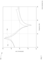
- FIG. 6 is a chart showing the relationship between Q BR and the number of layers in an acoustic Bragg reflector composed of alternating SiO 2 and diamond layers. Specifically, FIG. 6 is graph of Log 10 Q BR versus relative frequency with number of layers as a parameter. f 0 is the center frequency of the Bragg reflector, which is to say the frequency at which the effective thickness of the layers of the acoustic Bragg reflector are 1 ⁇ 4 wavelength.
- the solid line 610 is a plot of Q BR for SM XBARs with an acoustic Bragg reflector with 3 pairs of SiO 2 /Diamond layers (6 total layers).
- the dashed line 620 is a plot of Q BR for SM XBARs with an acoustic Bragg reflector with 2.5 pairs of SiO 2 /Diamond layers (5 total layers).
- the dot-dash line 630 is a plot of Q BR for SM XBARs with an acoustic Bragg reflector with 2 pairs of SiO 2 /Diamond layers (4 total layers).
- the dot-dot-dash line 640 is a plot of Q BR for SM XBARs with an acoustic Bragg reflector with 1.5 pairs of SiO 2 /Diamond layers (3 total layers).
- An acoustic Bragg reflector with 2.5 pairs of alternating SiO 2 and diamond layers may be sufficient for most XBAR filters.
- Acoustic Bragg reflectors using material other than SiO 2 and diamond may require more than 2.5 pairs of layers.
- the data shown in FIG. 6 results from simulation using a finite element method.
- FIG. 7 is a chart 700 of the normalized magnitude of the admittance (on a logarithmic scale) versus frequency for two representative SM XBARs having structures similar to the SM XBAR 500 of FIG. 5 .
- the data is FIG. 7 is based on simulation of the SM XBAR structures using a finite element method.
- the solid curve 710 is a plot of the magnitude of admittance of an SM XBAR including a Z-cut LN piezoelectric plate with a thickness tp of 71 nm.
- the pitch, width, and thickness of the aluminum IDT fingers are 1 ⁇ m, 250 nm, and 80 nm, respectively.
- the acoustic Bragg reflector includes three pairs of alternating SiO 2 and DLC layers with thicknesses of 40 nm and 136 nm, respectively. There is no front side dielectric layer.
- the resonance frequency Fr is 25.3 GHz
- the anti-resonance frequency Far is 27.3 GHz
- the R-aR bandwidth is 7.7%.
- R-aR bandwidth is defined as (Fr ⁇ Far)/Fr.
- the dashed curve 720 is a plot of the magnitude of admittance of an SM XBAR with the same construction as the previous example except the Bragg reflector is alternating SiO 2 and HfO 2 layers.
- the resonance frequency Fr is 25.5 GHz
- the anti-resonance frequency Far is 27.1 GHz
- the R-aR bandwidth is 6.2%.
- FIG. 8 is a schematic circuit diagram for a high frequency band-pass filter 800 using SM XBARs.
- the filter 800 has a conventional ladder filter architecture including four series resonators 810 A, 810 B, 810 C, 810 D and four shunt resonators 820 A, 820 B, 820 C, 820 D.
- the four series resonators 810 A, 810 B, 810 C, and 810 D are connected in series between a first port and a second port.
- the first and second ports are labeled “In” and “Out”, respectively.
- the filter 800 is reversible in that either port and serve as the input or output of the filter.
- the four shunt resonators 820 A, 820 B, 820 C, 820 D are connected from nodes between the series resonators to ground. All the shunt resonators and series resonators are SM XBARs.
- the filter 800 may include a substrate having a surface, a single-crystal piezoelectric plate having parallel front and back surfaces, and an acoustic Bragg reflector sandwiched between the surface of the substrate and the back surface of the single-crystal piezoelectric plate.
- the substrate, acoustic Bragg reflector, and piezoelectric plate are represented by the rectangle 830 in FIG. 8 .
- a conductor pattern formed on the front surface of the single-crystal piezoelectric plate includes interdigital transducers (IDTs) for each of the four series resonators 810 A, 8110 B, 810 C, 810 D and four shunt resonators 820 A, 820 B, 820 C, 820 D. All of the IDTs are configured to excite shear acoustic waves in the single-crystal piezoelectric plate in response to respective radio frequency signals applied to each IDT.
- IDTs interdigital transducers
- the resonance frequencies of shunt resonators are typically lower than the resonance frequencies of series resonators.
- the resonance frequency of an SM XBAR resonator is primarily determined by the thickness of the material stack above the acoustic Bragg reflector, which is to say the combined thickness of the piezoelectric plate and top side dielectric layer(s) if present.
- the resonance frequency of an SM XBAR is slightly dependent on IDT pitch and, to an even smaller extent, IDT finger width. IDT pitch and finger width also impacts other filter parameters including impedance and power handling capability.
- FIG. 9 A is a schematic cross-sectional view though a shunt resonator and a series resonator of a filter 900 A that uses dielectric thickness to separate the frequencies of shunt and series resonators.
- An acoustic Bragg reflector 940 is sandwiched between a piezoelectric plate 910 A and a substrate 920 .
- the piezoelectric plate 910 A has a uniform thickness.
- Interleaved IDT fingers, such as finger 930 are formed on the piezoelectric plate 910 A.
- a first dielectric layer 950 having a thickness t 1 , is deposited over the shunt resonator.
- a second dielectric layer 955 having a thickness t 2 is deposited over both the shunt and series resonator.
- a single dielectric layer having thickness t 1 +t 2 may be deposited over both the shunt and series resonators.
- the dielectric layer over the series resonator may then be thinned to thickness t 2 using a masked dry etching process.
- the difference between the overall thickness of the dielectric layers (t 1 +t 2 ) over the shunt resonator and the thickness t 2 of the dielectric layer over the series resonator defines a frequency offset between the series and shunt resonators.
- the second dielectric layer 955 may also serve to seal and passivate the surface of the filter 900 A.
- the second dielectric layer may be the same material as the first dielectric layer or a different material.
- the second dielectric layer may be a laminate of two or more sub-layers of different materials.
- an additional dielectric passivation layer (not shown in FIG. 9 A ) may be formed over the surface of the filter 900 A.
- the thickness of the final dielectric layer i.e. either the second dielectric layer 955 or an additional dielectric layer
- the final dielectric layer can be referred to as the “passivation and tuning layer”.
- FIG. 9 B is a schematic cross-sectional view though a shunt resonator and a series resonator of a filter 900 B that uses piezoelectric plate thickness to separate the frequencies of shunt and series resonators.
- An acoustic Bragg reflector 940 is sandwiched between a piezoelectric plate 910 B and a substrate 920 .
- Interleaved IDT fingers, such as finger 930 are formed on the diaphragms.
- the diaphragm of the shunt resonator has a thickness t 3 .
- the piezoelectric plate 910 B is selectively thinned (for example, as described in U.S. Pat. No.
- a passivation and tuning layer 955 may be deposited over both the shunt and series resonators.
- a filter using SM XBARS is not limited to either two dielectric thicknesses as shown in FIG. 9 A or two piezoelectric plate thicknesses as shown in FIG. 9 B .
- Filters may use three or more dielectric thicknesses, three or more piezoelectric plate thicknesses, or a combination of multiple dielectric thicknesses and multiple piezoelectric plate thicknesses.
- FIG. 10 is a chart 1000 illustrating the application of SM XB ARS in bandpass filters for K band communications devices.
- the solid curve 1010 is a plot of the magnitude of the input-output transfer function S(1,2) of an exemplary filter for 5G NR band n258.
- This filter includes eight SM XBARs connected in a ladder filter circuit as shown in FIG. 8 with shunt impedance matching inductors (not shown in FIG. 8 ) across the input and output ports.
- the data results from simulation of the filter using a finite element technique. All eight XBARs are on a common silicon substrate with a common acoustic Bragg reflector with 4 pairs of alternating SiO 2 and DLC layers.
- the piezoelectric plate is Z-cut LN with a thickness of 68 nm for series resonators and 79 nm for three of the four shunt resonators and 81.5 nm for the fourth shunt resonator.
- the IDT electrode are aluminum 90 nm thick.
- the pitch of the IDTs ranges from 0.775 ⁇ m to 1.1 ⁇ m.
- the IDT finger width to pitch ratio is 0.235 or 0.25 for all SM XBARs.
- the IDT pitch to piezoelectric plate thickness ratio ranges between 9.8 and 16.
- Resonance frequencies of shunt resonators are between 23.2 GHz and 24.2 GHz, which are below the lower edge of the filter passband.
- Resonance frequencies of series resonators are between 26.3 and 26.7 GHz, which are within the filter passband.
- FIG. 11 is a simplified flow chart of a method 1100 for making a SM XBAR or a filter incorporating SM XBARs.
- the method 1100 starts at 1110 with a piezoelectric film disposed on a sacrificial substrate 1102 and a device substrate 1104 .
- the method 1110 ends at 1195 with a completed SM XBAR or filter.
- the flow chart of FIG. 11 includes only major process steps.
- Various conventional process steps e.g. surface preparation, cleaning, inspection, baking, annealing, monitoring, testing, etc. may be performed before, between, after, and during the steps shown in FIG. 11 .
- Thin plates of single-crystal piezoelectric materials bonded to a non-piezoelectric substrate are commercially available. At the time of this application, both lithium niobate and lithium tantalate plates are available bonded to various substrates including silicon, quartz, and fused silica. Thin plates of other piezoelectric materials may be available now or in the future.
- the thickness of the piezoelectric plate may be between 50 nm and 200 nm.
- the thickness of the piezoelectric plate at 1102 may be equal to a desired final thickness. The thickness of the piezoelectric plate at 1102 may be greater than the final thickness and may be trimmed to the final thickness at a later step in the process 1100 .
- the piezoelectric plate 1102 may be, for example, z-cut lithium niobate bonded to a silicon wafer with an intervening SiO 2 layer.
- the device substrate 1104 may be silicon (as used in the previous examples) fused silica, quartz, or some other material.
- an acoustic Bragg reflector is formed by depositing alternating layers of materials having low and high acoustic impedance as previously described. Each of the layers has a thickness equal to or about one-fourth of the acoustic wavelength. The total number of layers in the acoustic Bragg reflector may typically be from five to eight.
- all of the layers of the acoustic Bragg reflector may be deposited on either the surface of the piezoelectric plate on the sacrificial substrate 1102 or a surface of the device substrate 1104 .
- some of the layers of the acoustic Bragg reflector may be deposited on the surface of the piezoelectric plate on the sacrificial substrate 1102 and the remaining layers of the acoustic Bragg reflector may be deposited on a surface of the device substrate 1104 .
- the piezoelectric plate on the sacrificial substrate 1102 and the device substrate 1104 may be bonded such that the layers of the acoustic Bragg reflector are sandwiched between the piezoelectric plate and the device substrate.
- the piezoelectric plate on the sacrificial substrate 1102 and the device substrate 1104 may be bonded using a wafer bonding process such as direct bonding, surface-activated or plasma-activated bonding, electrostatic bonding, or some other bonding technique. Note that, when one or more layers of the acoustic Bragg reflector are deposited on both the piezoelectric plate and the device substrate, the bonding will occur between or within layers of the acoustic Bragg reflector.
- the sacrificial substrate, and any intervening layers, are removed at 1140 to expose the surface of the piezoelectric plate (the surface that previously faced the sacrificial substrate).
- the sacrificial substrate may be removed, for example, by material-dependent wet or dry etching or some other process.
- a variation of the method from 1110 to 1140 starts with a single-crystal piezoelectric wafer at 1102 instead of a thin piezoelectric plate on a sacrificial substrate of a different material. Ions are implanted to a controlled depth beneath a surface of the piezoelectric wafer (not shown in FIG. 11 ). The portion of the wafer from the surface to the depth of the ion implantation is (or will become) the thin piezoelectric plate and the balance of the wafer is the sacrificial substrate.
- the acoustic Bragg reflector is formed at 1120 as previously described and the piezoelectric wafer and device substrate are bonded at 1130 such that the acoustic Bragg reflector is disposed between the ion-implanted surface of the piezoelectric wafer 1102 and the device substrate 1104 .
- the piezoelectric wafer may be split at the plane of the implanted ions (for example, using thermal shock), leaving a thin plate of piezoelectric material exposed and bonded to the acoustic Bragg reflector.
- the thickness of the thin plate piezoelectric material is determined by the energy (and thus depth) of the implanted ions.
- the process of ion implantation and subsequent separation of a thin plate is commonly referred to as “ion slicing”.
- the thickness of the piezoelectric plate after ion slicing may be equal to or greater than the desired final thickness.
- the thickness of the piezoelectric plate may be adjusted or trimmed to a desired final thickness.
- Trimming may include, for example, polishing or chemo-mechanical polishing the surface of the piezoelectric plate. Trimming may include globally or selectively removing material from the surface of the piezoelectric plate using an ion mill or other material removal tool. Trimming may include measuring a thickness profile of the piezoelectric plate and then removing material by polishing, ion milling, or some other technique based on the thickness profile to improve the thickness uniformity of the piezoelectric plate. Trimming may include applying a mask and removing material from selected regions of the piezoelectric plate (e.g. regions that will become series resonators). When fabricating filters for 27 GHz communications bands, the final thickness of the piezoelectric plate may be, for example, 50 nm to 90 nm.
- a conductor pattern including IDTs of each SM XBAR, is formed at 1150 by depositing and patterning one or more conductor layers on the trimmed surface of the piezoelectric plate.
- the conductor pattern may be, for example, aluminum, an aluminum alloy, copper, a copper alloy, or some other conductive metal.
- one or more layers of other materials may be disposed below (i.e. between the conductor layer and the piezoelectric plate) and/or on top of the conductor layer.
- a thin film of titanium, chrome, or other metal may be used to improve the adhesion between the conductor layer and the piezoelectric plate.
- the IDT finger thickness may be from 0.8 to 1.5 times the final thickness of the piezoelectric plate.
- a conduction enhancement layer of gold, aluminum, copper or other higher conductivity metal may be formed over portions of the conductor pattern (for example the IDT bus bars and interconnections between the IDTs).
- the conductor pattern may be formed at 1150 by depositing the conductor layer and, optionally, one or more other metal layers in sequence over the surface of the piezoelectric plate. The excess metal may then be removed by etching through patterned photoresist.
- the conductor layer can be etched, for example, by plasma etching, reactive ion etching, wet chemical etching, and other etching techniques.
- the conductor pattern may be formed at 1150 using a lift-off process.
- Photoresist may be deposited over the piezoelectric plate. and patterned to define the conductor pattern.
- the conductor layer and, optionally, one or more other layers may be deposited in sequence over the surface of the piezoelectric plate. The photoresist may then be removed, which removes the excess material, leaving the conductor pattern.
- one or more optional front-side dielectric layers may be formed by depositing one or more layers of dielectric material on the front side of the piezoelectric plate.
- the one or more dielectric layers may be deposited using a conventional deposition technique such as sputtering, evaporation, or chemical vapor deposition.
- the one or more dielectric layers may be deposited over the entire surface of the piezoelectric plate, including on top of the conductor pattern.
- one or more lithography processes (using photomasks) may be used to limit the deposition of the dielectric layers to selected areas of the piezoelectric plate, such as only between the interleaved fingers of the IDTs.
- Masks may also be used to allow deposition of different thicknesses of dielectric materials on different portions of the piezoelectric plate. For example, a first dielectric layer having a first thickness t 1 may be deposited over the IDTs of one or more shunt resonators. A second dielectric layer having a second thickness t 2 , where t 2 is equal to or greater than zero and less than t 1 , may be deposited over the IDTs of series resonators.
- the filter device may be completed at 1170 .
- Actions that may occur at 1170 including depositing and patterning additional metal layers to form conductors other than the IDT conductor pattern; depositing an encapsulation/passivation layer such as SiO 2 or Si 3 O 4 over all or a portion of the device; forming bonding pads or solder bumps or other means for making connection between the device and external circuitry; excising individual devices from a wafer containing multiple devices; other packaging steps; and testing.
- Another action that may occur at 1170 is to tune the resonant frequencies of the resonators within the device by adding or removing metal or dielectric material from the front side of the device. After the filter device is completed, the process ends at 1195 .
- “plurality” means two or more. As used herein, a “set” of items may include one or more of such items.
- the terms “comprising”, “including”, “carrying”, “having”, “containing”, “involving”, and the like are to be understood to be open-ended, i.e., to mean including but not limited to. Only the transitional phrases “consisting of” and “consisting essentially of”, respectively, are closed or semi-closed transitional phrases with respect to claims.
Landscapes
- Physics & Mathematics (AREA)
- Acoustics & Sound (AREA)
- Chemical & Material Sciences (AREA)
- Engineering & Computer Science (AREA)
- Crystallography & Structural Chemistry (AREA)
- Ceramic Engineering (AREA)
- Manufacturing & Machinery (AREA)
- Piezo-Electric Or Mechanical Vibrators, Or Delay Or Filter Circuits (AREA)
Abstract
Description
1/Q=1/Q BR+1/Q R+1/Q A+ . . . (1)
where Q is the overall Q-factor of the resonator and QBR, QR, and QA are the Q-factors for leakage through the Bragg grating, resistive losses, and acoustic losses, respectively. QBR is equivalent to the Q-factor of an otherwise ideal resonator with no losses other than leakage through the acoustic Bragg reflector. Many of these Q-factors are dependent on frequency.
Claims (18)
Priority Applications (2)
| Application Number | Priority Date | Filing Date | Title |
|---|---|---|---|
| US17/558,090 US12224732B2 (en) | 2018-06-15 | 2021-12-21 | Solidly-mounted transversely-excited film bulk acoustic resonators and filters for 27 GHz communications bands |
| US19/014,478 US20250150053A1 (en) | 2018-06-15 | 2025-01-09 | Solidly-mounted transversely-excited film bulk acoustic resonators and filters |
Applications Claiming Priority (14)
| Application Number | Priority Date | Filing Date | Title |
|---|---|---|---|
| US201862685825P | 2018-06-15 | 2018-06-15 | |
| US201862701363P | 2018-07-20 | 2018-07-20 | |
| US201862741702P | 2018-10-05 | 2018-10-05 | |
| US201862748883P | 2018-10-22 | 2018-10-22 | |
| US201862753809P | 2018-10-31 | 2018-10-31 | |
| US201862753815P | 2018-10-31 | 2018-10-31 | |
| US16/230,443 US10491192B1 (en) | 2018-06-15 | 2018-12-21 | Transversely-excited film bulk acoustic resonator |
| US201962818564P | 2019-03-14 | 2019-03-14 | |
| US16/438,141 US10601392B2 (en) | 2018-06-15 | 2019-06-11 | Solidly-mounted transversely-excited film bulk acoustic resonator |
| US16/779,306 US11165407B2 (en) | 2018-06-15 | 2020-01-31 | Solidly-mounted transversely-excited film bulk acoustic resonator |
| US202063000006P | 2020-03-26 | 2020-03-26 | |
| US16/896,147 US11264966B2 (en) | 2018-06-15 | 2020-06-08 | Solidly-mounted transversely-excited film bulk acoustic resonator with diamond layers in Bragg reflector stack |
| US202163251459P | 2021-10-01 | 2021-10-01 | |
| US17/558,090 US12224732B2 (en) | 2018-06-15 | 2021-12-21 | Solidly-mounted transversely-excited film bulk acoustic resonators and filters for 27 GHz communications bands |
Related Parent Applications (1)
| Application Number | Title | Priority Date | Filing Date |
|---|---|---|---|
| US16/896,147 Continuation-In-Part US11264966B2 (en) | 2018-06-15 | 2020-06-08 | Solidly-mounted transversely-excited film bulk acoustic resonator with diamond layers in Bragg reflector stack |
Related Child Applications (1)
| Application Number | Title | Priority Date | Filing Date |
|---|---|---|---|
| US19/014,478 Continuation US20250150053A1 (en) | 2018-06-15 | 2025-01-09 | Solidly-mounted transversely-excited film bulk acoustic resonators and filters |
Publications (2)
| Publication Number | Publication Date |
|---|---|
| US20220116010A1 US20220116010A1 (en) | 2022-04-14 |
| US12224732B2 true US12224732B2 (en) | 2025-02-11 |
Family
ID=81077957
Family Applications (2)
| Application Number | Title | Priority Date | Filing Date |
|---|---|---|---|
| US17/558,090 Active 2040-06-15 US12224732B2 (en) | 2018-06-15 | 2021-12-21 | Solidly-mounted transversely-excited film bulk acoustic resonators and filters for 27 GHz communications bands |
| US19/014,478 Pending US20250150053A1 (en) | 2018-06-15 | 2025-01-09 | Solidly-mounted transversely-excited film bulk acoustic resonators and filters |
Family Applications After (1)
| Application Number | Title | Priority Date | Filing Date |
|---|---|---|---|
| US19/014,478 Pending US20250150053A1 (en) | 2018-06-15 | 2025-01-09 | Solidly-mounted transversely-excited film bulk acoustic resonators and filters |
Country Status (1)
| Country | Link |
|---|---|
| US (2) | US12224732B2 (en) |
Families Citing this family (1)
| Publication number | Priority date | Publication date | Assignee | Title |
|---|---|---|---|---|
| WO2022085314A1 (en) * | 2020-10-23 | 2022-04-28 | 株式会社村田製作所 | Multiplexer, high-frequency module, and communication device |
Citations (219)
| Publication number | Priority date | Publication date | Assignee | Title |
|---|---|---|---|---|
| US5274345A (en) | 1992-05-13 | 1993-12-28 | Andersen Laboratories | Dual function reflector structures for interdigital saw transducer |
| US5446330A (en) | 1993-03-15 | 1995-08-29 | Matsushita Electric Industrial Co., Ltd. | Surface acoustic wave device having a lamination structure |
| US5552655A (en) | 1994-05-04 | 1996-09-03 | Trw Inc. | Low frequency mechanical resonator |
| US5631515A (en) | 1994-03-17 | 1997-05-20 | Fujitsu Limited | Surface acoustic wave device |
| US5726610A (en) | 1995-06-19 | 1998-03-10 | Motorola Inc. | Saw filter device for radio tranceiver utilizing different coupling coefficient ratios |
| JPH10209804A (en) | 1997-01-27 | 1998-08-07 | Oki Electric Ind Co Ltd | Surface acoustic wave resonator and surface acoustic wave filter |
| US5853601A (en) | 1997-04-03 | 1998-12-29 | Northrop Grumman Corporation | Top-via etch technique for forming dielectric membranes |
| JP2001244785A (en) | 2000-02-29 | 2001-09-07 | Kyocera Corp | Surface acoustic wave device |
| US6377140B1 (en) | 1999-07-09 | 2002-04-23 | Oki Electric Industry Co., Ltd. | Saw resonator filter with bridged-T configuration |
| US20020079986A1 (en) | 2000-12-21 | 2002-06-27 | Ruby Richard C. | Bulk acoustic resonator perimeter reflection system |
| US20020130736A1 (en) | 2001-03-19 | 2002-09-19 | Murata Manufacturing Co., Ltd | Edge-reflection surface acoustic wave filter |
| JP2002300003A (en) | 2001-03-29 | 2002-10-11 | Kyocera Corp | Elastic wave filter |
| US20020158714A1 (en) | 2001-04-27 | 2002-10-31 | Nokia Corporation | Method and system for wafer-level tuning of bulk acoustic wave resonators and filters by reducing thickness non-uniformity |
| US20020189062A1 (en) | 2001-06-15 | 2002-12-19 | Asia Pacific Microsystems, Inc. | Manufacturing method for a high quality film bulk acoustic wave device |
| US6516503B1 (en) | 1999-05-26 | 2003-02-11 | Murata Manufacturing Co., Ltd. | Method of making surface acoustic wave device |
| JP2003078389A (en) | 2001-08-31 | 2003-03-14 | Matsushita Electric Ind Co Ltd | Surface acoustic wave device and method of manufacturing the same |
| US6540827B1 (en) | 1998-02-17 | 2003-04-01 | Trustees Of Columbia University In The City Of New York | Slicing of single-crystal films using ion implantation |
| US20030080831A1 (en) | 2001-10-25 | 2003-05-01 | Naumenko Natalya F. | Surface acoustic wave devices using optimized cuts of lithium niobate (LiNbO3) |
| US6570470B2 (en) | 2000-06-30 | 2003-05-27 | Kyocera Corporation | Surface acoustic wave ladder filter utilizing parallel resonators with different resonant frequencies |
| US20030199105A1 (en) | 2002-04-22 | 2003-10-23 | Kub Francis J. | Method for making piezoelectric resonator and surface acoustic wave device using hydrogen implant layer splitting |
| US6670866B2 (en) | 2002-01-09 | 2003-12-30 | Nokia Corporation | Bulk acoustic wave resonator with two piezoelectric layers as balun in filters and duplexers |
| US20040041496A1 (en) | 2002-09-04 | 2004-03-04 | Fujitsu Media Devices Limited | Surface acoustic wave device, filter device and method of producing the surface acoustic wave device |
| US6707229B1 (en) | 1999-06-03 | 2004-03-16 | Tele Filter Zweigniederlassung Der Dover Germany Gmbh | Surface acoustic wave filter |
| JP2004129222A (en) | 2002-07-31 | 2004-04-22 | Murata Mfg Co Ltd | Piezoelectric component and method of manufacturing the same |
| US20040100164A1 (en) | 2002-11-26 | 2004-05-27 | Murata Manufacturing Co., Ltd. | Manufacturing method of electronic device |
| US20040207485A1 (en) | 2003-03-31 | 2004-10-21 | Osamu Kawachi | Surface acoustic wave device and method of fabricating the same |
| US6833774B2 (en) | 2002-06-25 | 2004-12-21 | Sawtek, Inc. | Surface acoustic wave filter |
| US20040261250A1 (en) | 2000-09-06 | 2004-12-30 | Murata Manufacturing Co., Ltd. | Method for adjusting a frequency characteristic of an edge reflection type surface acoustic wave device and method for producing an- edge reflection type surface acoustic wave device |
| US20050099091A1 (en) | 2003-11-12 | 2005-05-12 | Fujitsu Media Devices Limited | Elastic boundary wave device and method of manufacturing the same |
| US20050185026A1 (en) | 2004-01-26 | 2005-08-25 | Motohisa Noguchi | Piezoelectric element, piezoelectric actuator, ink jet recording head, ink jet printer, surface acoustic wave element, frequency filter, oscillator, electronic circuit, thin film piezoelectric resonator, and electronic apparatus |
| US20050218488A1 (en) | 2004-03-31 | 2005-10-06 | Mie Matsuo | Electronic component having micro-electrical mechanical system |
| US20050264136A1 (en) | 2004-05-31 | 2005-12-01 | Jun Tsutsumi | Surface acoustic wave device |
| US20060131731A1 (en) | 2004-11-22 | 2006-06-22 | Takao Sato | Midair semiconductor device and manufacturing method of the same |
| US20060152107A1 (en) | 2005-01-07 | 2006-07-13 | Seiko Epson Corporation | Lamb-wave high-frequency resonator |
| US20060179642A1 (en) | 2005-02-03 | 2006-08-17 | Kabushiki Kaisha Toshiba | Method for manufacturing a film bulk acoustic resonator |
| US20070090898A1 (en) | 2003-12-16 | 2007-04-26 | Murata Manufacturing Co., Ltd. | Boundary acoustic wave device |
| US20070115079A1 (en) | 2004-07-20 | 2007-05-24 | Murata Manufacturing Co., Ltd. | Piezoelectric filter |
| US20070182510A1 (en) | 2006-02-06 | 2007-08-09 | Samsung Electronics Co., Ltd. | Multi-band filter module and method of fabricating the same |
| US20070188047A1 (en) | 2006-02-16 | 2007-08-16 | Seiko Epson Corporation | Lamb wave type frequency device and method thereof |
| US20070194863A1 (en) | 2006-02-17 | 2007-08-23 | Kabushiki Kaisha Toshiba | Film bulk acoustic resonator and method of manufacturing same |
| US20070267942A1 (en) | 2006-05-19 | 2007-11-22 | Hisanori Matsumoto | Piezoelectric film resonator, radio-frequency filter using them, and radio-frequency module using them |
| US20070278898A1 (en) | 2006-06-06 | 2007-12-06 | Fujitsu Media Devices Limited | Acoustic boundary wave device, resonator and filter |
| US7312674B2 (en) | 2002-08-06 | 2007-12-25 | The Charles Stark Draper Laboratory, Inc. | Resonator system with a plurality of individual mechanically coupled resonators and method of making same |
| US20070296304A1 (en) | 2006-06-22 | 2007-12-27 | Seiko Epson Corporation | Acoustic wave device and method of manufacturing acoustic wave device |
| US20080018414A1 (en) | 2006-07-24 | 2008-01-24 | Fujitsu Media Devices Limited | Elastic wave device and manufacturing method of the same |
| US7345400B2 (en) | 2003-01-27 | 2008-03-18 | Murata Manufacturing Co., Ltd. | Surface acoustic wave device |
| US20080246559A1 (en) | 2007-01-19 | 2008-10-09 | Farrokh Ayazi | Lithographically-defined multi-standard multi-frequency high-Q tunable micromechanical resonators |
| US20080297280A1 (en) | 2007-05-31 | 2008-12-04 | Robert Thalhammer | Integrated Coupled Resonator Filter and Bulk Acoustic Wave Devices |
| US7463118B2 (en) | 2006-06-09 | 2008-12-09 | Texas Instruments Incorporated | Piezoelectric resonator with an efficient all-dielectric Bragg reflector |
| US7498904B2 (en) | 2005-06-08 | 2009-03-03 | Kabushiki Kaisha Toshiba | Piezoelectric thin film resonator and devices provided with the same |
| US7535152B2 (en) | 2005-10-19 | 2009-05-19 | Murata Manufacturing Co., Ltd. | Lamb wave device |
| US7554427B2 (en) | 2007-01-15 | 2009-06-30 | Hitachi Media Electronics Co., Ltd. | Thin film bulk acoustic wave resonator and filter, and radio frequency module using them |
| US20090273415A1 (en) | 2008-04-30 | 2009-11-05 | Avago Technologies Wireless Ip (Singapore) Pte. Ltd. | Bulk acoustic resonator electrical impedance transformers |
| US20100019866A1 (en) | 2008-07-23 | 2010-01-28 | Fujitsu Limited | Acoustic wave device, method of manufacturing acoustic wave device and transmission apparatus |
| JP2010062816A (en) | 2008-09-03 | 2010-03-18 | Murata Mfg Co Ltd | Acoustic wave filter |
| US7684109B2 (en) | 2007-02-28 | 2010-03-23 | Maxim Integrated Products, Inc. | Bragg mirror optimized for shear waves |
| WO2010047114A1 (en) | 2008-10-24 | 2010-04-29 | エプソントヨコム株式会社 | Surface acoustic wave resonator, surface acoustic wave oscillator, and surface acoustic wave modular device |
| JP2010103803A (en) | 2008-10-24 | 2010-05-06 | Epson Toyocom Corp | Surface acoustic wave resonator, surface acoustic wave oscillator, and surface acoustic wave module device |
| US20100123367A1 (en) | 2008-11-19 | 2010-05-20 | Ngk Insulators, Ltd. | Lamb wave device |
| US20100223999A1 (en) | 2009-03-03 | 2010-09-09 | Nihon Dempa Kogyo Co., Ltd. | Elastic wave device and electronic component |
| US20100301703A1 (en) | 2009-03-31 | 2010-12-02 | Sand9, Inc. | Integration of piezoelectric materials with substrates |
| US7868519B2 (en) | 2007-09-06 | 2011-01-11 | Murata Manufacturing Co., Ltd. | Piezoelectric resonator including an acoustic reflector portion |
| US20110018654A1 (en) | 2009-07-27 | 2011-01-27 | Avago Technologies Wireless Ip (Singapore) Pte. Ltd. | Resonator filter with multiple cross-couplings |
| US20110018389A1 (en) | 2008-01-30 | 2011-01-27 | Kyocera Corporation | Acoustic Wave Device and Method for Production of Same |
| US20110102107A1 (en) | 2008-02-05 | 2011-05-05 | Nihon Dempa Kogyo Co., Ltd. | Filter, portable terminal and electronic component |
| US7941103B2 (en) | 2005-11-15 | 2011-05-10 | Taiyo Yuden Co., Ltd. | Duplexer |
| US7939987B1 (en) | 2008-10-23 | 2011-05-10 | Triquint Semiconductor, Inc. | Acoustic wave device employing reflective elements for confining elastic energy |
| US20110109196A1 (en) | 2008-07-11 | 2011-05-12 | Goto Rei | Plate wave element and electronic equipment using same |
| US20110278993A1 (en) | 2010-05-17 | 2011-11-17 | Murata Manufacturing Co., Ltd. | Method for manufacturing composite piezoelectric substrate and piezoelectric device |
| US8278802B1 (en) | 2008-04-24 | 2012-10-02 | Rf Micro Devices, Inc. | Planarized sacrificial layer for MEMS fabrication |
| US8294330B1 (en) | 2009-03-31 | 2012-10-23 | Triquint Semiconductor, Inc. | High coupling, low loss saw filter and associated method |
| US20120286900A1 (en) | 2010-01-28 | 2012-11-15 | Murata Manufacturing Co., Ltd. | Tunable filter |
| US20120326809A1 (en) | 2010-03-12 | 2012-12-27 | Murata Manufacturing Co., Ltd. | Elastic wave resonator and ladder filter |
| US20130057360A1 (en) | 2010-04-23 | 2013-03-07 | Teknologian Tutkimuskeskus Vtt | Wide-band acoustically coupled thin-film baw filter |
| US20130127551A1 (en) | 2010-08-05 | 2013-05-23 | Adaptalog Limited | Crystal reference oscillator for navigation applications |
| US20130207747A1 (en) | 2010-12-28 | 2013-08-15 | Kyocera Corporation | Acoustic wave element and acoustic wave device using same |
| US20130234805A1 (en) | 2012-03-07 | 2013-09-12 | Taiyo Yuden Co., Ltd. | Resonator, frequency filter, duplexer, electronic device, and method of manufacturing resonator |
| US20130271238A1 (en) | 2012-04-13 | 2013-10-17 | Taiyo Yuden Co., Ltd. | Filter device, manufacturing method for filter device, and duplexer |
| US20130278609A1 (en) | 2012-04-19 | 2013-10-24 | Qualcomm Mems Technologies, Inc. | Isotropically-etched cavities for evanescent-mode electromagnetic-wave cavity resonators |
| US20130321100A1 (en) | 2012-06-05 | 2013-12-05 | Avago Technologies Wireless Ip (Singapore) Pte. Ltd. | Laterally-coupled acoustic resonators |
| US20140009032A1 (en) | 2012-07-04 | 2014-01-09 | Taiyo Yuden Co., Ltd. | Lamb wave device and manufacturing method thereof |
| US20140113571A1 (en) | 2012-10-18 | 2014-04-24 | Panasonic Corporation | Electronic device including filter |
| US20140130319A1 (en) | 2010-09-28 | 2014-05-15 | Murata Manufacturing Co., Ltd. | Method for manufacturing piezoelectric device |
| US20140145556A1 (en) | 2011-08-08 | 2014-05-29 | Murata Manufacturing Co., Ltd. | Elastic wave device |
| US20140152145A1 (en) | 2010-11-30 | 2014-06-05 | Murata Manufacturing Co., Ltd. | Elastic wave device and manufacturing method for same |
| US20140151151A1 (en) | 2010-10-15 | 2014-06-05 | Commissariat A L'energie Atomique Et Aux Energies Alternatives | Heterogenous acoustic structure formed from a homogeneous material |
| US20140173862A1 (en) | 2007-12-25 | 2014-06-26 | Murata Manufacturing Co., Ltd. | Method for manufacturing composite piezoelectric substrate |
| US20140225684A1 (en) | 2011-10-24 | 2014-08-14 | Murata Manufacturing Co., Ltd. | Surface acoustic wave device |
| US8816567B2 (en) | 2011-07-19 | 2014-08-26 | Qualcomm Mems Technologies, Inc. | Piezoelectric laterally vibrating resonator structure geometries for spurious frequency suppression |
| US8829766B2 (en) | 2008-08-01 | 2014-09-09 | Epcos Ag | Piezoelectric resonator operating in thickness shear mode |
| US20140312994A1 (en) | 2011-11-11 | 2014-10-23 | Teknologian tutkimuskeskut VTT | Laterally coupled bulk acoustic wave filter with improved passband characteristics |
| US8932686B2 (en) | 2008-10-31 | 2015-01-13 | Murata Manufacturing Co., Ltd. | Method for producing piezoelectric composite substrate |
| US20150042417A1 (en) | 2013-08-06 | 2015-02-12 | Murata Manufacturing Co., Ltd. | High-frequency module |
| JP2015054986A (en) | 2013-09-11 | 2015-03-23 | 太陽誘電株式会社 | Film deposition method of aluminum nitride film, manufacturing method of elastic wave device, and manufacturing apparatus of aluminum nitride film |
| US20150165479A1 (en) | 2013-12-12 | 2015-06-18 | Qualcomm Incorporated | Piezoelectric ultrasonic transducer and process |
| WO2015098694A1 (en) | 2013-12-26 | 2015-07-02 | 株式会社村田製作所 | Elastic wave device, and production method therefor |
| US20150244149A1 (en) | 2012-05-30 | 2015-08-27 | Euphoenix B.V. | Tunable Semiconductor Device And Method For Making Tunable Semiconductor Device |
| US9130145B2 (en) | 2012-03-29 | 2015-09-08 | Vectron International Gmbh | Surface acoustic wave component |
| US9148121B2 (en) | 2012-08-17 | 2015-09-29 | Taiyo Yuden Co., Ltd. | Acoustic wave filter, duplexer, and module |
| US9154111B2 (en) | 2011-05-20 | 2015-10-06 | Avago Technologies General Ip (Singapore) Pte. Ltd. | Double bulk acoustic resonator comprising aluminum scandium nitride |
| US20150319537A1 (en) | 2012-12-12 | 2015-11-05 | Epcos Ag | Electroacoustic Components and Methods Thereof |
| US20150365067A1 (en) | 2013-03-21 | 2015-12-17 | Ngk Insulators, Ltd. | Composite Substrates for Acoustic Wave Elements, and Acoustic Wave Elements |
| JP2016001923A (en) | 2013-02-27 | 2016-01-07 | 京セラ株式会社 | Acoustic wave device, splitter, and communication module |
| US9240768B2 (en) | 2011-11-22 | 2016-01-19 | Taiyo Yuden Co., Ltd. | Duplexer with transmission and reception filters each including resonators formed on different chips |
| US20160028367A1 (en) | 2014-07-25 | 2016-01-28 | Akoustis, Inc. | Single crystal acoustic resonator and bulk acoustic wave filter |
| WO2016017104A1 (en) | 2014-07-31 | 2016-02-04 | Skyworks Panasonic Filter Solutions Japan Co., Ltd. | Acoustic wave filters and duplexers using same |
| US9276557B1 (en) | 2013-07-01 | 2016-03-01 | Sandia Corporation | Programmable electroacoustic filter apparatus and method for its manufacture |
| US20160079958A1 (en) | 2014-05-30 | 2016-03-17 | Avago Technologies General Ip (Singapore) Pte. Ltd. | Acoustic resonator comprising vertically extended acoustic cavity |
| US20160087187A1 (en) | 2014-05-29 | 2016-03-24 | Avago Technologies General Ip (Singapore) Pte. Ltd. | Capacitive coupled resonator and filter device with comb electrodes and support pillars separating piezoelectric layer |
| WO2016052129A1 (en) | 2014-09-30 | 2016-04-07 | 株式会社村田製作所 | Acoustic wave device and method for manufacturing same |
| US9369105B1 (en) | 2007-08-31 | 2016-06-14 | Rf Micro Devices, Inc. | Method for manufacturing a vibrating MEMS circuit |
| US20160182009A1 (en) | 2014-12-17 | 2016-06-23 | Rf Micro Devices, Inc. | Plate wave devices with wave confinement structures and fabrication methods |
| US9425765B2 (en) | 2013-04-22 | 2016-08-23 | Northeastern University | Nano- and micro-electromechanical resonators |
| WO2016147687A1 (en) | 2015-03-13 | 2016-09-22 | 株式会社村田製作所 | Elastic wave device and production method for same |
| US20160301382A1 (en) | 2013-12-25 | 2016-10-13 | Murata Manufacturing Co., Ltd. | Electronic component module |
| US9525398B1 (en) | 2014-05-27 | 2016-12-20 | Sandia Corporation | Single crystal micromechanical resonator and fabrication methods thereof |
| US20170063332A1 (en) | 2015-08-25 | 2017-03-02 | Avago Technologies General Ip (Singapore) Pte. Ltd. | Surface acoustic wave (saw) resonator having trap-rich region |
| US20170104470A1 (en) | 2015-10-09 | 2017-04-13 | Avago Technologies General Ip (Singapore) Pte. Ltd. | Interdigitated transducers and reflectors for surface acoustic wave devices with non-uniformly spaced elements |
| US9640750B2 (en) | 2011-03-25 | 2017-05-02 | Skyworks Filter Solutions Japan Co., Ltd. | Acoustic wave device with suppressed higher order transverse modes |
| CN106788318A (en) | 2016-11-22 | 2017-05-31 | 山东科技大学 | A kind of method for manufacturing FBAR on a flexible substrate |
| US20170179225A1 (en) | 2011-05-25 | 2017-06-22 | Semiconductor Components Industries, Llc | Semiconductor device having a super junction structure and method of manufacturing the same |
| US20170179928A1 (en) | 2015-11-13 | 2017-06-22 | Resonant Inc. | Acoustic wave filter with enhanced rejection |
| US20170201232A1 (en) | 2016-01-07 | 2017-07-13 | Taiyo Yuden Co., Ltd. | Acoustic wave device and method of fabricating the same |
| US20170214387A1 (en) | 2016-01-26 | 2017-07-27 | Avago Technologies General Ip (Singapore) Pte. Ltd. | Bulk acoustic wave resonator with piezoelectric layer comprising lithium niobate or lithium tantalate |
| US20170214381A1 (en) | 2016-01-22 | 2017-07-27 | Rf Micro Devices, Inc. | Guided wave devices with selectively thinned piezoelectric layers |
| US20170222617A1 (en) | 2014-10-16 | 2017-08-03 | Murata Manufacturing Co., Ltd. | High-frequency module |
| US20170222622A1 (en) | 2016-01-28 | 2017-08-03 | Triquint Semiconductor, Inc. | Surface acoustic wave device having a piezoelectric layer on a quartz substrate and methods of manufacturing thereof |
| US9762202B2 (en) | 2008-12-17 | 2017-09-12 | Analog Devices, Inc. | Method of manufacturing a mechanical resonating structure |
| US20170264266A1 (en) | 2014-12-25 | 2017-09-14 | Murata Manufacturing Co., Ltd. | Acoustic wave device and manufacturing method for same |
| US9780759B2 (en) | 2010-12-24 | 2017-10-03 | Murata Manufacturing Co., Ltd. | Elastic wave device and method for manufacturing the same |
| US20170290160A1 (en) | 2016-04-01 | 2017-10-05 | Skyworks Filter Solutions Japan Co., Ltd. | Electronic package including cavity defined by resin and method of forming same |
| WO2017188342A1 (en) | 2016-04-27 | 2017-11-02 | 京セラ株式会社 | Elastic wave element and communication device |
| US9837984B2 (en) | 2014-12-24 | 2017-12-05 | Qorvo Us, Inc. | RF ladder filter with simplified acoustic RF resonator parallel capacitance compensation |
| US20170370791A1 (en) | 2016-06-28 | 2017-12-28 | Taiyo Yuden Co., Ltd. | Method of fabricating acoustic wave device and acoustic wave device |
| WO2018003273A1 (en) | 2016-06-28 | 2018-01-04 | 株式会社村田製作所 | Multiplexer, high-frequency front end circuit, and communication device |
| US20180005950A1 (en) | 2016-06-29 | 2018-01-04 | Murata Manufacturing Co., Ltd. | Electronic component device, method of mounting electronic component device on circuit board, and mounting structure of electronic component device on circuit board |
| WO2018003268A1 (en) | 2016-06-28 | 2018-01-04 | 株式会社村田製作所 | Elastic wave filter device, multiplexer, high-frequency front end circuit, and communication device |
| US20180013400A1 (en) | 2016-07-05 | 2018-01-11 | Taiyo Yuden Co., Ltd. | Acoustic wave device |
| US20180013405A1 (en) | 2015-04-30 | 2018-01-11 | Murata Manufacturing Co., Ltd. | Ladder filter and duplexer |
| US20180026603A1 (en) | 2015-05-22 | 2018-01-25 | Murata Manufacturing Co., Ltd. | Electronic component |
| US20180033952A1 (en) | 2016-07-28 | 2018-02-01 | Taiyo Yuden Co., Ltd. | Electronic device and method of fabricating the same |
| US20180041191A1 (en) | 2016-08-08 | 2018-02-08 | Samsung Electro-Mechanics Co., Ltd. | Saw filter device and method of manufacturing the same |
| US20180062615A1 (en) | 2015-05-08 | 2018-03-01 | Murata Manufacturing Co., Ltd. | High frequency module |
| US20180062617A1 (en) | 2016-08-25 | 2018-03-01 | Qualcomm Incorporated | Single-chip multi-frequency film bulk acoustic-wave resonators |
| US20180123016A1 (en) | 2012-06-15 | 2018-05-03 | Carnegie Mellon University | Microelectronic structures with suspended lithium-based thin films |
| JP2018093487A (en) | 2016-11-30 | 2018-06-14 | スカイワークス ソリューションズ, インコーポレイテッドSkyworks Solutions, Inc. | Saw filter that comprises piezoelectric substrate having stepwise cross section |
| US20180191322A1 (en) | 2017-01-03 | 2018-07-05 | Win Semiconductors Corp. | Method for fabricating bulk acoustic wave resonator with mass adjustment structure |
| US20180212589A1 (en) | 2010-10-14 | 2018-07-26 | Teknologian Tutkimuskeskus Vtt Oy | Wide-band acoustically coupled thin-film baw filter |
| WO2018163860A1 (en) | 2017-03-06 | 2018-09-13 | 株式会社村田製作所 | Elastic wave device, high-frequency front end circuit, communication device and method for manufacturing elastic wave device |
| US10079414B2 (en) | 2015-03-17 | 2018-09-18 | The United States Of America, As Represented By The Secretary Of The Navy | Switched multiplexer with flat group delay and channelized limiting |
| US20180278227A1 (en) | 2017-03-24 | 2018-09-27 | Dror Hurwitz | Method for fabricating rf resonators and filters |
| JP2018166259A (en) | 2017-03-28 | 2018-10-25 | 京セラ株式会社 | Elastic wave element |
| JP2018207144A (en) | 2017-05-30 | 2018-12-27 | 太陽誘電株式会社 | Elastic wave device |
| US20190007022A1 (en) | 2017-03-31 | 2019-01-03 | Ngk Insulators, Ltd. | Bonded bodies and acoustic wave devices |
| US10187039B2 (en) | 2016-06-07 | 2019-01-22 | Skyworks Filter Solutions Japan Co., Ltd. | Filter devices having reduced spurious emissions from lamb waves |
| US10200013B2 (en) | 2016-02-18 | 2019-02-05 | X-Celeprint Limited | Micro-transfer-printed acoustic wave filter device |
| US20190068155A1 (en) | 2016-06-07 | 2019-02-28 | Murata Manufacturing Co., Ltd. | Elastic wave device and method for producing the same |
| US20190068164A1 (en) | 2016-03-11 | 2019-02-28 | Akoustis, Inc. | 5G BAND n79 ACOUSTIC WAVE RESONATOR RF FILTER CIRCUIT |
| US20190074813A1 (en) | 2017-09-01 | 2019-03-07 | Skyworks Solutions, Inc. | Piston mode lamb wave resonators |
| US20190131953A1 (en) | 2017-10-31 | 2019-05-02 | The Board Of Trustees Of The University Of Illinois | Interdigital transducers on a piezoelectric thin-film for signal compression |
| US10284176B1 (en) | 2015-06-03 | 2019-05-07 | Qorvo Us, Inc. | Temperature compensated surface acoustic wave device and methods of manufacturing the same |
| US20190148621A1 (en) | 2016-03-11 | 2019-05-16 | Akoustis, Inc. | Method of manufacture for single crystal acoustic resonator devices using micro-vias |
| US20190181825A1 (en) | 2017-12-07 | 2019-06-13 | Infineon Technologies Ag | System and method for a radio frequency filter |
| US20190181833A1 (en) | 2016-08-26 | 2019-06-13 | Murata Manufacturing Co., Ltd. | Acoustic wave filter device, multiplexer, radio frequency front-end circuit, and communication device |
| US20190207583A1 (en) | 2017-12-28 | 2019-07-04 | Taiyo Yuden Co., Ltd. | Acoustic wave device, filter, and multiplexer |
| WO2019138810A1 (en) | 2018-01-12 | 2019-07-18 | 株式会社村田製作所 | Elastic wave device, multiplexer, high-frequency front end circuit, and communication device |
| US20190245518A1 (en) | 2016-10-28 | 2019-08-08 | Kyocera Corporation | Acoustic wave filter, acoustic wave device, multiplexer, and communication apparatus |
| US10389391B2 (en) | 2016-01-29 | 2019-08-20 | Kyocera Corporation | Acoustic wave resonator, acoustic wave filter, multiplexer, and communication apparatus |
| US20190273480A1 (en) | 2018-03-02 | 2019-09-05 | Skyworks Solutions, Inc. | Lamb wave loop circuit for acoustic wave filter |
| CN110417373A (en) | 2019-07-25 | 2019-11-05 | 华南理工大学 | A kind of adjustable lateral field excitation thin film bulk acoustic wave resonator of frequency and preparation method |
| US20190348966A1 (en) | 2018-05-10 | 2019-11-14 | Globalfoundries Singapore Pte. Ltd. | Acoustic wave filter formed on a v-groove topography and method for producing the same |
| US10491192B1 (en) | 2018-06-15 | 2019-11-26 | Resonant Inc. | Transversely-excited film bulk acoustic resonator |
| US20190379351A1 (en) | 2017-03-13 | 2019-12-12 | Murata Manufacturing Co., Ltd. | Notch filter |
| US20190386636A1 (en) | 2018-06-15 | 2019-12-19 | Resonant Inc. | Transversely-excited film bulk acoustic resonator |
| US20200007110A1 (en) | 2017-03-15 | 2020-01-02 | Murata Manufacturing Co., Ltd. | Acoustic wave element, acoustic wave filter device, and multiplexer |
| US20200021271A1 (en) | 2018-06-15 | 2020-01-16 | Resonant Inc. | Transversely-excited film bulk acoustic resonators for high power applications |
| US20200021272A1 (en) | 2018-07-10 | 2020-01-16 | Texas Instruments Incorporated | Laterally Vibrating Bulk Acoustic Wave Resonator |
| US20200036357A1 (en) | 2017-04-26 | 2020-01-30 | Murata Manufacturing Co., Ltd. | Acoustic wave device |
| US10601392B2 (en) | 2018-06-15 | 2020-03-24 | Resonant Inc. | Solidly-mounted transversely-excited film bulk acoustic resonator |
| CN210431367U (en) | 2019-07-25 | 2020-04-28 | 华南理工大学 | Transverse field excitation film bulk acoustic resonator with adjustable frequency |
| WO2020092414A2 (en) | 2018-10-31 | 2020-05-07 | Resonant Inc. | Solidly-mounted transversely-excited film bulk acoustic resonator |
| WO2020100744A1 (en) | 2018-11-16 | 2020-05-22 | 株式会社村田製作所 | Elastic wave device |
| US20200228087A1 (en) | 2019-01-16 | 2020-07-16 | Murata Manufacturing Co., Ltd. | Acoustic wave device |
| US20200235719A1 (en) | 2018-06-15 | 2020-07-23 | Resonant Inc. | Xbar resonators with non-rectangular diaphragms |
| US20200244247A1 (en) | 2019-01-30 | 2020-07-30 | Murata Manufacturing Co., Ltd. | Acoustic wave filter |
| US20200259480A1 (en) | 2019-02-08 | 2020-08-13 | Vtt Technical Research Centre Of Finland Ltd | Low loss acoustic device |
| US20200295729A1 (en) | 2019-03-14 | 2020-09-17 | Resonant Inc. | Transversely-excited film bulk acoustic resonator with partial bragg reflectors |
| US20200304091A1 (en) | 2018-06-15 | 2020-09-24 | Resonant Inc. | Solidly-mounted transversely-excited film bulk acoustic resonator with diamond layers in bragg reflector stack |
| US10790802B2 (en) | 2018-06-15 | 2020-09-29 | Resonant Inc. | Transversely excited film bulk acoustic resonator using rotated Y-X cut lithium niobate |
| US20200313645A1 (en) | 2019-03-25 | 2020-10-01 | Skyworks Solutions, Inc. | Acoustic wave filters with isolation |
| US10797675B2 (en) | 2018-06-15 | 2020-10-06 | Resonant Inc. | Transversely excited film bulk acoustic resonator using rotated z-cut lithium niobate |
| US10812048B2 (en) | 2016-09-02 | 2020-10-20 | Murata Manufacturing Co., Ltd. | Acoustic wave filter device, radio-frequency front-end circuit, and communication apparatus |
| US10819319B1 (en) | 2018-11-20 | 2020-10-27 | Impinj, Inc. | Level shifter circuit with self-gated transition amplifier |
| US10819309B1 (en) | 2019-04-05 | 2020-10-27 | Resonant Inc. | Transversely-excited film bulk acoustic resonator package and method |
| US10826462B2 (en) | 2018-06-15 | 2020-11-03 | Resonant Inc. | Transversely-excited film bulk acoustic resonators with molybdenum conductors |
| US20200350891A1 (en) | 2018-06-15 | 2020-11-05 | Resonant Inc. | Transversely-excited film bulk acoustic resonator with etch-stop layer |
| US10868513B2 (en) | 2018-06-15 | 2020-12-15 | Resonant Inc. | Transversely-excited film bulk acoustic filters with symmetric layout |
| US10868510B2 (en) | 2018-06-15 | 2020-12-15 | Resonant Inc. | Transversely-excited film bulk acoustic resonator with half-lambda dielectric layer |
| US20210013859A1 (en) | 2018-06-15 | 2021-01-14 | Resonant Inc. | Transversely-excited film bulk acoustic resonator with etched conductor patterns |
| US10911021B2 (en) | 2019-06-27 | 2021-02-02 | Resonant Inc. | Transversely-excited film bulk acoustic resonator with lateral etch stop |
| US10917072B2 (en) | 2019-06-24 | 2021-02-09 | Resonant Inc. | Split ladder acoustic wave filters |
| US10985728B2 (en) | 2018-06-15 | 2021-04-20 | Resonant Inc. | Transversely-excited film bulk acoustic resonator and filter with a uniform-thickness dielectric overlayer |
| US10992284B2 (en) | 2018-06-15 | 2021-04-27 | Resonant Inc. | Filter using transversely-excited film bulk acoustic resonators with multiple frequency setting layers |
| US10992283B2 (en) | 2018-06-15 | 2021-04-27 | Resonant Inc. | High power transversely-excited film bulk acoustic resonators on rotated Z-cut lithium niobate |
| US10992282B1 (en) | 2020-06-18 | 2021-04-27 | Resonant Inc. | Transversely-excited film bulk acoustic resonators with electrodes having a second layer of variable width |
| US10998877B2 (en) | 2018-06-15 | 2021-05-04 | Resonant Inc. | Film bulk acoustic resonator fabrication method with frequency trimming based on electric measurements prior to cavity etch |
| US11003971B2 (en) | 2017-11-07 | 2021-05-11 | Resonant Inc. | Ultra-wide-band saw sensor with hyperbolically frequency-modulated etched reflector |
| US20210273631A1 (en) | 2020-02-28 | 2021-09-02 | Resonant Inc. | Split-ladder band n77 filter using transversely-excited film bulk acoustic resonators |
| US11143561B2 (en) | 2018-12-05 | 2021-10-12 | Resonant Inc. | Passive microphone/pressure sensor using a piezoelectric diaphragm |
| US11146238B2 (en) | 2018-06-15 | 2021-10-12 | Resonant Inc. | Film bulk acoustic resonator fabrication method |
| US11146232B2 (en) | 2018-06-15 | 2021-10-12 | Resonant Inc. | Transversely-excited film bulk acoustic resonator with reduced spurious modes |
| US20210328574A1 (en) | 2020-04-20 | 2021-10-21 | Resonant Inc. | Small transversely-excited film bulk acoustic resonators with enhanced q-factor |
| US11171629B2 (en) | 2018-06-15 | 2021-11-09 | Resonant Inc. | Transversely-excited film bulk acoustic resonator using pre-formed cavities |
| US11201601B2 (en) | 2018-06-15 | 2021-12-14 | Resonant Inc. | Transversely-excited film bulk acoustic resonator with multiple diaphragm thicknesses and fabrication method |
| US20220103160A1 (en) | 2020-02-28 | 2022-03-31 | Resonant Inc. | Filter using transversely-excited film bulk acoustic resonators with inductively coupled sub-resonators |
| US20220116014A1 (en) | 2020-10-13 | 2022-04-14 | RF360 Europe GmbH | Surface acoustic wave (saw) device with high permittivity dielectric for intermodulation distortion improvement |
| US11323089B2 (en) | 2018-06-15 | 2022-05-03 | Resonant Inc. | Filter using piezoelectric film bonded to high resistivity silicon substrate with trap-rich layer |
| US20220149808A1 (en) | 2020-11-11 | 2022-05-12 | Resonant Inc. | Transversely-excited film bulk acoustic resonator with low thermal impedance |
| US20220200567A1 (en) | 2018-06-15 | 2022-06-23 | Resonant Inc. | Transversely-excited film bulk acoustic resonator using yx-cut lithium niobate for high power applications |
-
2021
- 2021-12-21 US US17/558,090 patent/US12224732B2/en active Active
-
2025
- 2025-01-09 US US19/014,478 patent/US20250150053A1/en active Pending
Patent Citations (264)
| Publication number | Priority date | Publication date | Assignee | Title |
|---|---|---|---|---|
| US5274345A (en) | 1992-05-13 | 1993-12-28 | Andersen Laboratories | Dual function reflector structures for interdigital saw transducer |
| US5446330A (en) | 1993-03-15 | 1995-08-29 | Matsushita Electric Industrial Co., Ltd. | Surface acoustic wave device having a lamination structure |
| US5631515A (en) | 1994-03-17 | 1997-05-20 | Fujitsu Limited | Surface acoustic wave device |
| US5552655A (en) | 1994-05-04 | 1996-09-03 | Trw Inc. | Low frequency mechanical resonator |
| US5726610A (en) | 1995-06-19 | 1998-03-10 | Motorola Inc. | Saw filter device for radio tranceiver utilizing different coupling coefficient ratios |
| JPH10209804A (en) | 1997-01-27 | 1998-08-07 | Oki Electric Ind Co Ltd | Surface acoustic wave resonator and surface acoustic wave filter |
| US5853601A (en) | 1997-04-03 | 1998-12-29 | Northrop Grumman Corporation | Top-via etch technique for forming dielectric membranes |
| US6540827B1 (en) | 1998-02-17 | 2003-04-01 | Trustees Of Columbia University In The City Of New York | Slicing of single-crystal films using ion implantation |
| US6710514B2 (en) | 1999-05-26 | 2004-03-23 | Murata Manufacturing Co., Ltd. | Surface acoustic wave device |
| US6516503B1 (en) | 1999-05-26 | 2003-02-11 | Murata Manufacturing Co., Ltd. | Method of making surface acoustic wave device |
| US6707229B1 (en) | 1999-06-03 | 2004-03-16 | Tele Filter Zweigniederlassung Der Dover Germany Gmbh | Surface acoustic wave filter |
| US6377140B1 (en) | 1999-07-09 | 2002-04-23 | Oki Electric Industry Co., Ltd. | Saw resonator filter with bridged-T configuration |
| JP2001244785A (en) | 2000-02-29 | 2001-09-07 | Kyocera Corp | Surface acoustic wave device |
| US6570470B2 (en) | 2000-06-30 | 2003-05-27 | Kyocera Corporation | Surface acoustic wave ladder filter utilizing parallel resonators with different resonant frequencies |
| US20040261250A1 (en) | 2000-09-06 | 2004-12-30 | Murata Manufacturing Co., Ltd. | Method for adjusting a frequency characteristic of an edge reflection type surface acoustic wave device and method for producing an- edge reflection type surface acoustic wave device |
| US20020079986A1 (en) | 2000-12-21 | 2002-06-27 | Ruby Richard C. | Bulk acoustic resonator perimeter reflection system |
| US20020130736A1 (en) | 2001-03-19 | 2002-09-19 | Murata Manufacturing Co., Ltd | Edge-reflection surface acoustic wave filter |
| JP2002300003A (en) | 2001-03-29 | 2002-10-11 | Kyocera Corp | Elastic wave filter |
| US20020158714A1 (en) | 2001-04-27 | 2002-10-31 | Nokia Corporation | Method and system for wafer-level tuning of bulk acoustic wave resonators and filters by reducing thickness non-uniformity |
| US20020189062A1 (en) | 2001-06-15 | 2002-12-19 | Asia Pacific Microsystems, Inc. | Manufacturing method for a high quality film bulk acoustic wave device |
| JP2003078389A (en) | 2001-08-31 | 2003-03-14 | Matsushita Electric Ind Co Ltd | Surface acoustic wave device and method of manufacturing the same |
| US20030080831A1 (en) | 2001-10-25 | 2003-05-01 | Naumenko Natalya F. | Surface acoustic wave devices using optimized cuts of lithium niobate (LiNbO3) |
| US6670866B2 (en) | 2002-01-09 | 2003-12-30 | Nokia Corporation | Bulk acoustic wave resonator with two piezoelectric layers as balun in filters and duplexers |
| US20030199105A1 (en) | 2002-04-22 | 2003-10-23 | Kub Francis J. | Method for making piezoelectric resonator and surface acoustic wave device using hydrogen implant layer splitting |
| US6833774B2 (en) | 2002-06-25 | 2004-12-21 | Sawtek, Inc. | Surface acoustic wave filter |
| JP2004129222A (en) | 2002-07-31 | 2004-04-22 | Murata Mfg Co Ltd | Piezoelectric component and method of manufacturing the same |
| US20040207033A1 (en) | 2002-07-31 | 2004-10-21 | Yoshihiro Koshido | Piezoelectric component and production method therefor |
| US7312674B2 (en) | 2002-08-06 | 2007-12-25 | The Charles Stark Draper Laboratory, Inc. | Resonator system with a plurality of individual mechanically coupled resonators and method of making same |
| JP2004096677A (en) | 2002-09-04 | 2004-03-25 | Fujitsu Media Device Kk | Surface acoustic wave device, filter device and method of manufacturing the same |
| US20040041496A1 (en) | 2002-09-04 | 2004-03-04 | Fujitsu Media Devices Limited | Surface acoustic wave device, filter device and method of producing the surface acoustic wave device |
| US20040100164A1 (en) | 2002-11-26 | 2004-05-27 | Murata Manufacturing Co., Ltd. | Manufacturing method of electronic device |
| US7345400B2 (en) | 2003-01-27 | 2008-03-18 | Murata Manufacturing Co., Ltd. | Surface acoustic wave device |
| US20040207485A1 (en) | 2003-03-31 | 2004-10-21 | Osamu Kawachi | Surface acoustic wave device and method of fabricating the same |
| JP2004304622A (en) | 2003-03-31 | 2004-10-28 | Fujitsu Media Device Kk | Surface acoustic wave device and method of manufacturing the same |
| US20050099091A1 (en) | 2003-11-12 | 2005-05-12 | Fujitsu Media Devices Limited | Elastic boundary wave device and method of manufacturing the same |
| US20070090898A1 (en) | 2003-12-16 | 2007-04-26 | Murata Manufacturing Co., Ltd. | Boundary acoustic wave device |
| US20050185026A1 (en) | 2004-01-26 | 2005-08-25 | Motohisa Noguchi | Piezoelectric element, piezoelectric actuator, ink jet recording head, ink jet printer, surface acoustic wave element, frequency filter, oscillator, electronic circuit, thin film piezoelectric resonator, and electronic apparatus |
| US20050218488A1 (en) | 2004-03-31 | 2005-10-06 | Mie Matsuo | Electronic component having micro-electrical mechanical system |
| US20050264136A1 (en) | 2004-05-31 | 2005-12-01 | Jun Tsutsumi | Surface acoustic wave device |
| US20070115079A1 (en) | 2004-07-20 | 2007-05-24 | Murata Manufacturing Co., Ltd. | Piezoelectric filter |
| US20060131731A1 (en) | 2004-11-22 | 2006-06-22 | Takao Sato | Midair semiconductor device and manufacturing method of the same |
| JP2006173557A (en) | 2004-11-22 | 2006-06-29 | Toshiba Corp | Hollow semiconductor device and manufacturing method thereof |
| US20060152107A1 (en) | 2005-01-07 | 2006-07-13 | Seiko Epson Corporation | Lamb-wave high-frequency resonator |
| US20060179642A1 (en) | 2005-02-03 | 2006-08-17 | Kabushiki Kaisha Toshiba | Method for manufacturing a film bulk acoustic resonator |
| US7498904B2 (en) | 2005-06-08 | 2009-03-03 | Kabushiki Kaisha Toshiba | Piezoelectric thin film resonator and devices provided with the same |
| US7535152B2 (en) | 2005-10-19 | 2009-05-19 | Murata Manufacturing Co., Ltd. | Lamb wave device |
| US7941103B2 (en) | 2005-11-15 | 2011-05-10 | Taiyo Yuden Co., Ltd. | Duplexer |
| US20070182510A1 (en) | 2006-02-06 | 2007-08-09 | Samsung Electronics Co., Ltd. | Multi-band filter module and method of fabricating the same |
| US20100064492A1 (en) | 2006-02-16 | 2010-03-18 | Seiko Epson Corporation | Lamb wave type frequency device and method thereof |
| JP2007251910A (en) | 2006-02-16 | 2007-09-27 | Seiko Epson Corp | Lamb wave type high frequency device, manufacturing method of lamb wave type high frequency device |
| US20070188047A1 (en) | 2006-02-16 | 2007-08-16 | Seiko Epson Corporation | Lamb wave type frequency device and method thereof |
| US7728483B2 (en) | 2006-02-16 | 2010-06-01 | Seiko Epson Corporation | Lamb wave type frequency device and method thereof |
| US20070194863A1 (en) | 2006-02-17 | 2007-08-23 | Kabushiki Kaisha Toshiba | Film bulk acoustic resonator and method of manufacturing same |
| US20070267942A1 (en) | 2006-05-19 | 2007-11-22 | Hisanori Matsumoto | Piezoelectric film resonator, radio-frequency filter using them, and radio-frequency module using them |
| JP2007329584A (en) | 2006-06-06 | 2007-12-20 | Fujitsu Media Device Kk | Boundary acoustic wave element, resonator and filter |
| US20070278898A1 (en) | 2006-06-06 | 2007-12-06 | Fujitsu Media Devices Limited | Acoustic boundary wave device, resonator and filter |
| US7463118B2 (en) | 2006-06-09 | 2008-12-09 | Texas Instruments Incorporated | Piezoelectric resonator with an efficient all-dielectric Bragg reflector |
| US20070296304A1 (en) | 2006-06-22 | 2007-12-27 | Seiko Epson Corporation | Acoustic wave device and method of manufacturing acoustic wave device |
| US20080018414A1 (en) | 2006-07-24 | 2008-01-24 | Fujitsu Media Devices Limited | Elastic wave device and manufacturing method of the same |
| US7554427B2 (en) | 2007-01-15 | 2009-06-30 | Hitachi Media Electronics Co., Ltd. | Thin film bulk acoustic wave resonator and filter, and radio frequency module using them |
| US20080246559A1 (en) | 2007-01-19 | 2008-10-09 | Farrokh Ayazi | Lithographically-defined multi-standard multi-frequency high-Q tunable micromechanical resonators |
| US7684109B2 (en) | 2007-02-28 | 2010-03-23 | Maxim Integrated Products, Inc. | Bragg mirror optimized for shear waves |
| US20080297280A1 (en) | 2007-05-31 | 2008-12-04 | Robert Thalhammer | Integrated Coupled Resonator Filter and Bulk Acoustic Wave Devices |
| US9369105B1 (en) | 2007-08-31 | 2016-06-14 | Rf Micro Devices, Inc. | Method for manufacturing a vibrating MEMS circuit |
| US7868519B2 (en) | 2007-09-06 | 2011-01-11 | Murata Manufacturing Co., Ltd. | Piezoelectric resonator including an acoustic reflector portion |
| US20140173862A1 (en) | 2007-12-25 | 2014-06-26 | Murata Manufacturing Co., Ltd. | Method for manufacturing composite piezoelectric substrate |
| US20110018389A1 (en) | 2008-01-30 | 2011-01-27 | Kyocera Corporation | Acoustic Wave Device and Method for Production of Same |
| US20110102107A1 (en) | 2008-02-05 | 2011-05-05 | Nihon Dempa Kogyo Co., Ltd. | Filter, portable terminal and electronic component |
| US8278802B1 (en) | 2008-04-24 | 2012-10-02 | Rf Micro Devices, Inc. | Planarized sacrificial layer for MEMS fabrication |
| US20090273415A1 (en) | 2008-04-30 | 2009-11-05 | Avago Technologies Wireless Ip (Singapore) Pte. Ltd. | Bulk acoustic resonator electrical impedance transformers |
| US20110109196A1 (en) | 2008-07-11 | 2011-05-12 | Goto Rei | Plate wave element and electronic equipment using same |
| US20100019866A1 (en) | 2008-07-23 | 2010-01-28 | Fujitsu Limited | Acoustic wave device, method of manufacturing acoustic wave device and transmission apparatus |
| US8829766B2 (en) | 2008-08-01 | 2014-09-09 | Epcos Ag | Piezoelectric resonator operating in thickness shear mode |
| JP2010062816A (en) | 2008-09-03 | 2010-03-18 | Murata Mfg Co Ltd | Acoustic wave filter |
| US7939987B1 (en) | 2008-10-23 | 2011-05-10 | Triquint Semiconductor, Inc. | Acoustic wave device employing reflective elements for confining elastic energy |
| JP2010103803A (en) | 2008-10-24 | 2010-05-06 | Epson Toyocom Corp | Surface acoustic wave resonator, surface acoustic wave oscillator, and surface acoustic wave module device |
| WO2010047114A1 (en) | 2008-10-24 | 2010-04-29 | エプソントヨコム株式会社 | Surface acoustic wave resonator, surface acoustic wave oscillator, and surface acoustic wave modular device |
| US8344815B2 (en) | 2008-10-24 | 2013-01-01 | Seiko Epson Corporation | Surface acoustic wave resonator, surface acoustic wave oscillator, and surface acoustic wave module unit |
| US8932686B2 (en) | 2008-10-31 | 2015-01-13 | Murata Manufacturing Co., Ltd. | Method for producing piezoelectric composite substrate |
| US7965015B2 (en) | 2008-11-19 | 2011-06-21 | Ngk Insulators, Ltd. | Lamb wave device |
| US20100123367A1 (en) | 2008-11-19 | 2010-05-20 | Ngk Insulators, Ltd. | Lamb wave device |
| US9762202B2 (en) | 2008-12-17 | 2017-09-12 | Analog Devices, Inc. | Method of manufacturing a mechanical resonating structure |
| JP2010233210A (en) | 2009-03-03 | 2010-10-14 | Nippon Dempa Kogyo Co Ltd | Elastic wave device and electronic component |
| US20100223999A1 (en) | 2009-03-03 | 2010-09-09 | Nihon Dempa Kogyo Co., Ltd. | Elastic wave device and electronic component |
| US20100301703A1 (en) | 2009-03-31 | 2010-12-02 | Sand9, Inc. | Integration of piezoelectric materials with substrates |
| US8294330B1 (en) | 2009-03-31 | 2012-10-23 | Triquint Semiconductor, Inc. | High coupling, low loss saw filter and associated method |
| US20110018654A1 (en) | 2009-07-27 | 2011-01-27 | Avago Technologies Wireless Ip (Singapore) Pte. Ltd. | Resonator filter with multiple cross-couplings |
| US20120286900A1 (en) | 2010-01-28 | 2012-11-15 | Murata Manufacturing Co., Ltd. | Tunable filter |
| US20120326809A1 (en) | 2010-03-12 | 2012-12-27 | Murata Manufacturing Co., Ltd. | Elastic wave resonator and ladder filter |
| US20150333730A1 (en) | 2010-04-23 | 2015-11-19 | Teknologian Tutkimuskeskus Vtt Oy | Wide-band acoustically coupled thin-film BAW filter |
| JP2013528996A (en) | 2010-04-23 | 2013-07-11 | テクノロジアン テュトキムスケスクス ヴェーテーテー | Broadband acoustic coupling thin film BAW filter |
| US20130057360A1 (en) | 2010-04-23 | 2013-03-07 | Teknologian Tutkimuskeskus Vtt | Wide-band acoustically coupled thin-film baw filter |
| US20110278993A1 (en) | 2010-05-17 | 2011-11-17 | Murata Manufacturing Co., Ltd. | Method for manufacturing composite piezoelectric substrate and piezoelectric device |
| US20130127551A1 (en) | 2010-08-05 | 2013-05-23 | Adaptalog Limited | Crystal reference oscillator for navigation applications |
| US20140130319A1 (en) | 2010-09-28 | 2014-05-15 | Murata Manufacturing Co., Ltd. | Method for manufacturing piezoelectric device |
| US20180212589A1 (en) | 2010-10-14 | 2018-07-26 | Teknologian Tutkimuskeskus Vtt Oy | Wide-band acoustically coupled thin-film baw filter |
| US20140151151A1 (en) | 2010-10-15 | 2014-06-05 | Commissariat A L'energie Atomique Et Aux Energies Alternatives | Heterogenous acoustic structure formed from a homogeneous material |
| US9748923B2 (en) | 2010-11-30 | 2017-08-29 | Murata Manufacturing Co., Ltd. | Elastic wave device and manufacturing method for same |
| US20140152145A1 (en) | 2010-11-30 | 2014-06-05 | Murata Manufacturing Co., Ltd. | Elastic wave device and manufacturing method for same |
| US9780759B2 (en) | 2010-12-24 | 2017-10-03 | Murata Manufacturing Co., Ltd. | Elastic wave device and method for manufacturing the same |
| US20130207747A1 (en) | 2010-12-28 | 2013-08-15 | Kyocera Corporation | Acoustic wave element and acoustic wave device using same |
| US9640750B2 (en) | 2011-03-25 | 2017-05-02 | Skyworks Filter Solutions Japan Co., Ltd. | Acoustic wave device with suppressed higher order transverse modes |
| US9154111B2 (en) | 2011-05-20 | 2015-10-06 | Avago Technologies General Ip (Singapore) Pte. Ltd. | Double bulk acoustic resonator comprising aluminum scandium nitride |
| US20170179225A1 (en) | 2011-05-25 | 2017-06-22 | Semiconductor Components Industries, Llc | Semiconductor device having a super junction structure and method of manufacturing the same |
| US8816567B2 (en) | 2011-07-19 | 2014-08-26 | Qualcomm Mems Technologies, Inc. | Piezoelectric laterally vibrating resonator structure geometries for spurious frequency suppression |
| US20140145556A1 (en) | 2011-08-08 | 2014-05-29 | Murata Manufacturing Co., Ltd. | Elastic wave device |
| US20140225684A1 (en) | 2011-10-24 | 2014-08-14 | Murata Manufacturing Co., Ltd. | Surface acoustic wave device |
| US9219466B2 (en) | 2011-11-11 | 2015-12-22 | Teknologian Tutkimuskeskus Vtt Oy | Laterally coupled bulk acoustic wave filter with improved passband characteristics |
| US20140312994A1 (en) | 2011-11-11 | 2014-10-23 | Teknologian tutkimuskeskut VTT | Laterally coupled bulk acoustic wave filter with improved passband characteristics |
| US9240768B2 (en) | 2011-11-22 | 2016-01-19 | Taiyo Yuden Co., Ltd. | Duplexer with transmission and reception filters each including resonators formed on different chips |
| US9112134B2 (en) | 2012-03-07 | 2015-08-18 | Taiyo Yuden Co., Ltd. | Resonator, frequency filter, duplexer, electronic device, and method of manufacturing resonator |
| JP2013214954A (en) | 2012-03-07 | 2013-10-17 | Taiyo Yuden Co Ltd | Resonator, frequency filter, duplexer, electronic device, and method for manufacturing resonator |
| US20130234805A1 (en) | 2012-03-07 | 2013-09-12 | Taiyo Yuden Co., Ltd. | Resonator, frequency filter, duplexer, electronic device, and method of manufacturing resonator |
| US9130145B2 (en) | 2012-03-29 | 2015-09-08 | Vectron International Gmbh | Surface acoustic wave component |
| US20130271238A1 (en) | 2012-04-13 | 2013-10-17 | Taiyo Yuden Co., Ltd. | Filter device, manufacturing method for filter device, and duplexer |
| US20130278609A1 (en) | 2012-04-19 | 2013-10-24 | Qualcomm Mems Technologies, Inc. | Isotropically-etched cavities for evanescent-mode electromagnetic-wave cavity resonators |
| US20150244149A1 (en) | 2012-05-30 | 2015-08-27 | Euphoenix B.V. | Tunable Semiconductor Device And Method For Making Tunable Semiconductor Device |
| US9093979B2 (en) | 2012-06-05 | 2015-07-28 | Avago Technologies General Ip (Singapore) Pte. Ltd. | Laterally-coupled acoustic resonators |
| US20130321100A1 (en) | 2012-06-05 | 2013-12-05 | Avago Technologies Wireless Ip (Singapore) Pte. Ltd. | Laterally-coupled acoustic resonators |
| US20180123016A1 (en) | 2012-06-15 | 2018-05-03 | Carnegie Mellon University | Microelectronic structures with suspended lithium-based thin films |
| US20140009032A1 (en) | 2012-07-04 | 2014-01-09 | Taiyo Yuden Co., Ltd. | Lamb wave device and manufacturing method thereof |
| US9148121B2 (en) | 2012-08-17 | 2015-09-29 | Taiyo Yuden Co., Ltd. | Acoustic wave filter, duplexer, and module |
| US20140113571A1 (en) | 2012-10-18 | 2014-04-24 | Panasonic Corporation | Electronic device including filter |
| US20150319537A1 (en) | 2012-12-12 | 2015-11-05 | Epcos Ag | Electroacoustic Components and Methods Thereof |
| JP2016001923A (en) | 2013-02-27 | 2016-01-07 | 京セラ株式会社 | Acoustic wave device, splitter, and communication module |
| US20160049920A1 (en) | 2013-02-27 | 2016-02-18 | Kyocera Corporation | Acoustic wave element, duplexer, and communication module |
| US20150365067A1 (en) | 2013-03-21 | 2015-12-17 | Ngk Insulators, Ltd. | Composite Substrates for Acoustic Wave Elements, and Acoustic Wave Elements |
| US9425765B2 (en) | 2013-04-22 | 2016-08-23 | Northeastern University | Nano- and micro-electromechanical resonators |
| US9276557B1 (en) | 2013-07-01 | 2016-03-01 | Sandia Corporation | Programmable electroacoustic filter apparatus and method for its manufacture |
| US20150042417A1 (en) | 2013-08-06 | 2015-02-12 | Murata Manufacturing Co., Ltd. | High-frequency module |
| JP2015054986A (en) | 2013-09-11 | 2015-03-23 | 太陽誘電株式会社 | Film deposition method of aluminum nitride film, manufacturing method of elastic wave device, and manufacturing apparatus of aluminum nitride film |
| US20150165479A1 (en) | 2013-12-12 | 2015-06-18 | Qualcomm Incorporated | Piezoelectric ultrasonic transducer and process |
| US20160301382A1 (en) | 2013-12-25 | 2016-10-13 | Murata Manufacturing Co., Ltd. | Electronic component module |
| US20160285430A1 (en) | 2013-12-26 | 2016-09-29 | Murata Manufacturing Co., Ltd. | Elastic wave device and fabrication method thereof |
| WO2015098694A1 (en) | 2013-12-26 | 2015-07-02 | 株式会社村田製作所 | Elastic wave device, and production method therefor |
| US9525398B1 (en) | 2014-05-27 | 2016-12-20 | Sandia Corporation | Single crystal micromechanical resonator and fabrication methods thereof |
| US20160087187A1 (en) | 2014-05-29 | 2016-03-24 | Avago Technologies General Ip (Singapore) Pte. Ltd. | Capacitive coupled resonator and filter device with comb electrodes and support pillars separating piezoelectric layer |
| US20160079958A1 (en) | 2014-05-30 | 2016-03-17 | Avago Technologies General Ip (Singapore) Pte. Ltd. | Acoustic resonator comprising vertically extended acoustic cavity |
| US20160028367A1 (en) | 2014-07-25 | 2016-01-28 | Akoustis, Inc. | Single crystal acoustic resonator and bulk acoustic wave filter |
| WO2016017104A1 (en) | 2014-07-31 | 2016-02-04 | Skyworks Panasonic Filter Solutions Japan Co., Ltd. | Acoustic wave filters and duplexers using same |
| WO2016052129A1 (en) | 2014-09-30 | 2016-04-07 | 株式会社村田製作所 | Acoustic wave device and method for manufacturing same |
| US20170187352A1 (en) | 2014-09-30 | 2017-06-29 | Murata Manufacturing Co., Ltd. | Elastic wave device and manufacturing method therefor |
| US20170222617A1 (en) | 2014-10-16 | 2017-08-03 | Murata Manufacturing Co., Ltd. | High-frequency module |
| US20160182009A1 (en) | 2014-12-17 | 2016-06-23 | Rf Micro Devices, Inc. | Plate wave devices with wave confinement structures and fabrication methods |
| US9837984B2 (en) | 2014-12-24 | 2017-12-05 | Qorvo Us, Inc. | RF ladder filter with simplified acoustic RF resonator parallel capacitance compensation |
| US20170264266A1 (en) | 2014-12-25 | 2017-09-14 | Murata Manufacturing Co., Ltd. | Acoustic wave device and manufacturing method for same |
| WO2016147687A1 (en) | 2015-03-13 | 2016-09-22 | 株式会社村田製作所 | Elastic wave device and production method for same |
| US10079414B2 (en) | 2015-03-17 | 2018-09-18 | The United States Of America, As Represented By The Secretary Of The Navy | Switched multiplexer with flat group delay and channelized limiting |
| US20180013405A1 (en) | 2015-04-30 | 2018-01-11 | Murata Manufacturing Co., Ltd. | Ladder filter and duplexer |
| US20180062615A1 (en) | 2015-05-08 | 2018-03-01 | Murata Manufacturing Co., Ltd. | High frequency module |
| US20180026603A1 (en) | 2015-05-22 | 2018-01-25 | Murata Manufacturing Co., Ltd. | Electronic component |
| US10284176B1 (en) | 2015-06-03 | 2019-05-07 | Qorvo Us, Inc. | Temperature compensated surface acoustic wave device and methods of manufacturing the same |
| US20170063332A1 (en) | 2015-08-25 | 2017-03-02 | Avago Technologies General Ip (Singapore) Pte. Ltd. | Surface acoustic wave (saw) resonator having trap-rich region |
| US20170104470A1 (en) | 2015-10-09 | 2017-04-13 | Avago Technologies General Ip (Singapore) Pte. Ltd. | Interdigitated transducers and reflectors for surface acoustic wave devices with non-uniformly spaced elements |
| US20170179928A1 (en) | 2015-11-13 | 2017-06-22 | Resonant Inc. | Acoustic wave filter with enhanced rejection |
| US20170201232A1 (en) | 2016-01-07 | 2017-07-13 | Taiyo Yuden Co., Ltd. | Acoustic wave device and method of fabricating the same |
| US20170214381A1 (en) | 2016-01-22 | 2017-07-27 | Rf Micro Devices, Inc. | Guided wave devices with selectively thinned piezoelectric layers |
| US10211806B2 (en) | 2016-01-22 | 2019-02-19 | Qorvo Us, Inc. | Guided wave devices with embedded electrodes and non-embedded electrodes |
| US20170214387A1 (en) | 2016-01-26 | 2017-07-27 | Avago Technologies General Ip (Singapore) Pte. Ltd. | Bulk acoustic wave resonator with piezoelectric layer comprising lithium niobate or lithium tantalate |
| US20170222622A1 (en) | 2016-01-28 | 2017-08-03 | Triquint Semiconductor, Inc. | Surface acoustic wave device having a piezoelectric layer on a quartz substrate and methods of manufacturing thereof |
| US10389391B2 (en) | 2016-01-29 | 2019-08-20 | Kyocera Corporation | Acoustic wave resonator, acoustic wave filter, multiplexer, and communication apparatus |
| US10200013B2 (en) | 2016-02-18 | 2019-02-05 | X-Celeprint Limited | Micro-transfer-printed acoustic wave filter device |
| US20190068164A1 (en) | 2016-03-11 | 2019-02-28 | Akoustis, Inc. | 5G BAND n79 ACOUSTIC WAVE RESONATOR RF FILTER CIRCUIT |
| US20190148621A1 (en) | 2016-03-11 | 2019-05-16 | Akoustis, Inc. | Method of manufacture for single crystal acoustic resonator devices using micro-vias |
| US20170290160A1 (en) | 2016-04-01 | 2017-10-05 | Skyworks Filter Solutions Japan Co., Ltd. | Electronic package including cavity defined by resin and method of forming same |
| WO2017188342A1 (en) | 2016-04-27 | 2017-11-02 | 京セラ株式会社 | Elastic wave element and communication device |
| US20190068155A1 (en) | 2016-06-07 | 2019-02-28 | Murata Manufacturing Co., Ltd. | Elastic wave device and method for producing the same |
| US10187039B2 (en) | 2016-06-07 | 2019-01-22 | Skyworks Filter Solutions Japan Co., Ltd. | Filter devices having reduced spurious emissions from lamb waves |
| WO2018003273A1 (en) | 2016-06-28 | 2018-01-04 | 株式会社村田製作所 | Multiplexer, high-frequency front end circuit, and communication device |
| US10644674B2 (en) | 2016-06-28 | 2020-05-05 | Murata Manufacturing Co., Ltd. | Multiplexer, radio-frequency front-end circuit, and communication device |
| US20190123721A1 (en) | 2016-06-28 | 2019-04-25 | Murata Manufacturing Co., Ltd. | Multiplexer, radio-frequency front-end circuit, and communication device |
| WO2018003268A1 (en) | 2016-06-28 | 2018-01-04 | 株式会社村田製作所 | Elastic wave filter device, multiplexer, high-frequency front end circuit, and communication device |
| US20170370791A1 (en) | 2016-06-28 | 2017-12-28 | Taiyo Yuden Co., Ltd. | Method of fabricating acoustic wave device and acoustic wave device |
| US20180005950A1 (en) | 2016-06-29 | 2018-01-04 | Murata Manufacturing Co., Ltd. | Electronic component device, method of mounting electronic component device on circuit board, and mounting structure of electronic component device on circuit board |
| US20180013400A1 (en) | 2016-07-05 | 2018-01-11 | Taiyo Yuden Co., Ltd. | Acoustic wave device |
| US20180033952A1 (en) | 2016-07-28 | 2018-02-01 | Taiyo Yuden Co., Ltd. | Electronic device and method of fabricating the same |
| US20180041191A1 (en) | 2016-08-08 | 2018-02-08 | Samsung Electro-Mechanics Co., Ltd. | Saw filter device and method of manufacturing the same |
| US20180062617A1 (en) | 2016-08-25 | 2018-03-01 | Qualcomm Incorporated | Single-chip multi-frequency film bulk acoustic-wave resonators |
| US20190181833A1 (en) | 2016-08-26 | 2019-06-13 | Murata Manufacturing Co., Ltd. | Acoustic wave filter device, multiplexer, radio frequency front-end circuit, and communication device |
| US10812048B2 (en) | 2016-09-02 | 2020-10-20 | Murata Manufacturing Co., Ltd. | Acoustic wave filter device, radio-frequency front-end circuit, and communication apparatus |
| US20190245518A1 (en) | 2016-10-28 | 2019-08-08 | Kyocera Corporation | Acoustic wave filter, acoustic wave device, multiplexer, and communication apparatus |
| CN106788318A (en) | 2016-11-22 | 2017-05-31 | 山东科技大学 | A kind of method for manufacturing FBAR on a flexible substrate |
| JP2018093487A (en) | 2016-11-30 | 2018-06-14 | スカイワークス ソリューションズ, インコーポレイテッドSkyworks Solutions, Inc. | Saw filter that comprises piezoelectric substrate having stepwise cross section |
| US20180191322A1 (en) | 2017-01-03 | 2018-07-05 | Win Semiconductors Corp. | Method for fabricating bulk acoustic wave resonator with mass adjustment structure |
| US20190386638A1 (en) | 2017-03-06 | 2019-12-19 | Murata Manufacturing Co., Ltd. | Acoustic wave device, high frequency front end circuit, communication apparatus, and manufacturing method for acoustic wave device |
| WO2018163860A1 (en) | 2017-03-06 | 2018-09-13 | 株式会社村田製作所 | Elastic wave device, high-frequency front end circuit, communication device and method for manufacturing elastic wave device |
| US20190379351A1 (en) | 2017-03-13 | 2019-12-12 | Murata Manufacturing Co., Ltd. | Notch filter |
| US20200007110A1 (en) | 2017-03-15 | 2020-01-02 | Murata Manufacturing Co., Ltd. | Acoustic wave element, acoustic wave filter device, and multiplexer |
| US20180278227A1 (en) | 2017-03-24 | 2018-09-27 | Dror Hurwitz | Method for fabricating rf resonators and filters |
| JP2018166259A (en) | 2017-03-28 | 2018-10-25 | 京セラ株式会社 | Elastic wave element |
| US20190007022A1 (en) | 2017-03-31 | 2019-01-03 | Ngk Insulators, Ltd. | Bonded bodies and acoustic wave devices |
| US20200036357A1 (en) | 2017-04-26 | 2020-01-30 | Murata Manufacturing Co., Ltd. | Acoustic wave device |
| JP2018207144A (en) | 2017-05-30 | 2018-12-27 | 太陽誘電株式会社 | Elastic wave device |
| US20190074813A1 (en) | 2017-09-01 | 2019-03-07 | Skyworks Solutions, Inc. | Piston mode lamb wave resonators |
| US20190131953A1 (en) | 2017-10-31 | 2019-05-02 | The Board Of Trustees Of The University Of Illinois | Interdigital transducers on a piezoelectric thin-film for signal compression |
| US11003971B2 (en) | 2017-11-07 | 2021-05-11 | Resonant Inc. | Ultra-wide-band saw sensor with hyperbolically frequency-modulated etched reflector |
| US20190181825A1 (en) | 2017-12-07 | 2019-06-13 | Infineon Technologies Ag | System and method for a radio frequency filter |
| US20190207583A1 (en) | 2017-12-28 | 2019-07-04 | Taiyo Yuden Co., Ltd. | Acoustic wave device, filter, and multiplexer |
| WO2019138810A1 (en) | 2018-01-12 | 2019-07-18 | 株式会社村田製作所 | Elastic wave device, multiplexer, high-frequency front end circuit, and communication device |
| US20190273480A1 (en) | 2018-03-02 | 2019-09-05 | Skyworks Solutions, Inc. | Lamb wave loop circuit for acoustic wave filter |
| US20190348966A1 (en) | 2018-05-10 | 2019-11-14 | Globalfoundries Singapore Pte. Ltd. | Acoustic wave filter formed on a v-groove topography and method for producing the same |
| US20190386636A1 (en) | 2018-06-15 | 2019-12-19 | Resonant Inc. | Transversely-excited film bulk acoustic resonator |
| US10911017B2 (en) | 2018-06-15 | 2021-02-02 | Resonant Inc. | Solidly mounted transversely excited film bulk acoustic resonator using rotated Z-cut lithium niobate |
| US20200021271A1 (en) | 2018-06-15 | 2020-01-16 | Resonant Inc. | Transversely-excited film bulk acoustic resonators for high power applications |
| US10601392B2 (en) | 2018-06-15 | 2020-03-24 | Resonant Inc. | Solidly-mounted transversely-excited film bulk acoustic resonator |
| US11949399B2 (en) * | 2018-06-15 | 2024-04-02 | Murata Manufacturing Co., Ltd. | Solidly-mounted transversely-excited film bulk acoustic resonator with diamond layers in Bragg reflector stack |
| US10637438B2 (en) | 2018-06-15 | 2020-04-28 | Resonant Inc. | Transversely-excited film bulk acoustic resonators for high power applications |
| US20190386635A1 (en) | 2018-06-15 | 2019-12-19 | Resonant Inc. | Transversely-excited film bulk acoustic resonator |
| US20220200567A1 (en) | 2018-06-15 | 2022-06-23 | Resonant Inc. | Transversely-excited film bulk acoustic resonator using yx-cut lithium niobate for high power applications |
| US11323089B2 (en) | 2018-06-15 | 2022-05-03 | Resonant Inc. | Filter using piezoelectric film bonded to high resistivity silicon substrate with trap-rich layer |
| US11201601B2 (en) | 2018-06-15 | 2021-12-14 | Resonant Inc. | Transversely-excited film bulk acoustic resonator with multiple diaphragm thicknesses and fabrication method |
| US20200235719A1 (en) | 2018-06-15 | 2020-07-23 | Resonant Inc. | Xbar resonators with non-rectangular diaphragms |
| US11171629B2 (en) | 2018-06-15 | 2021-11-09 | Resonant Inc. | Transversely-excited film bulk acoustic resonator using pre-formed cavities |
| US11165407B2 (en) | 2018-06-15 | 2021-11-02 | Resonant Inc. | Solidly-mounted transversely-excited film bulk acoustic resonator |
| US11146232B2 (en) | 2018-06-15 | 2021-10-12 | Resonant Inc. | Transversely-excited film bulk acoustic resonator with reduced spurious modes |
| US10756697B2 (en) | 2018-06-15 | 2020-08-25 | Resonant Inc. | Transversely-excited film bulk acoustic resonator |
| US11146238B2 (en) | 2018-06-15 | 2021-10-12 | Resonant Inc. | Film bulk acoustic resonator fabrication method |
| US20200304091A1 (en) | 2018-06-15 | 2020-09-24 | Resonant Inc. | Solidly-mounted transversely-excited film bulk acoustic resonator with diamond layers in bragg reflector stack |
| US10790802B2 (en) | 2018-06-15 | 2020-09-29 | Resonant Inc. | Transversely excited film bulk acoustic resonator using rotated Y-X cut lithium niobate |
| US11146244B2 (en) | 2018-06-15 | 2021-10-12 | Resonant Inc. | Solidly-mounted transversely excited film bulk acoustic resonator using rotated Y-X cut lithium niobate |
| US10797675B2 (en) | 2018-06-15 | 2020-10-06 | Resonant Inc. | Transversely excited film bulk acoustic resonator using rotated z-cut lithium niobate |
| US10491192B1 (en) | 2018-06-15 | 2019-11-26 | Resonant Inc. | Transversely-excited film bulk acoustic resonator |
| US11146231B2 (en) | 2018-06-15 | 2021-10-12 | Resonant Inc. | Solidly-mounted transversely-excited film bulk acoustic resonator with recessed interdigital transducer fingers |
| US11139794B2 (en) | 2018-06-15 | 2021-10-05 | Resonant Inc. | Transversely-excited film bulk acoustic resonator |
| US10826462B2 (en) | 2018-06-15 | 2020-11-03 | Resonant Inc. | Transversely-excited film bulk acoustic resonators with molybdenum conductors |
| US20200350891A1 (en) | 2018-06-15 | 2020-11-05 | Resonant Inc. | Transversely-excited film bulk acoustic resonator with etch-stop layer |
| US10868513B2 (en) | 2018-06-15 | 2020-12-15 | Resonant Inc. | Transversely-excited film bulk acoustic filters with symmetric layout |
| US10868510B2 (en) | 2018-06-15 | 2020-12-15 | Resonant Inc. | Transversely-excited film bulk acoustic resonator with half-lambda dielectric layer |
| US10868512B2 (en) | 2018-06-15 | 2020-12-15 | Resonant Inc. | High power transversely-excited film bulk acoustic resonators on Z-cut lithium niobate |
| US20210013859A1 (en) | 2018-06-15 | 2021-01-14 | Resonant Inc. | Transversely-excited film bulk acoustic resonator with etched conductor patterns |
| US11114996B2 (en) | 2018-06-15 | 2021-09-07 | Resonant Inc. | Transversely-excited film bulk acoustic resonators with molybdenum conductors |
| US10911023B2 (en) | 2018-06-15 | 2021-02-02 | Resonant Inc. | Transversely-excited film bulk acoustic resonator with etch-stop layer |
| US11114998B2 (en) | 2018-06-15 | 2021-09-07 | Resonant Inc. | Transversely-excited film bulk acoustic resonators for high power applications |
| US10998882B2 (en) | 2018-06-15 | 2021-05-04 | Resonant Inc. | XBAR resonators with non-rectangular diaphragms |
| US10917070B2 (en) | 2018-06-15 | 2021-02-09 | Resonant Inc. | Bandpass filter with frequency separation between shunt and series resonators set by dielectric layer thickness |
| US10985730B2 (en) | 2018-06-15 | 2021-04-20 | Resonant Inc. | Filter devices having high power transversely-excited film bulk acoustic resonators |
| US10985726B2 (en) | 2018-06-15 | 2021-04-20 | Resonant Inc. | Transversely excited film bulk acoustic resonator with recessed interdigital transducer fingers |
| US10985728B2 (en) | 2018-06-15 | 2021-04-20 | Resonant Inc. | Transversely-excited film bulk acoustic resonator and filter with a uniform-thickness dielectric overlayer |
| US10992284B2 (en) | 2018-06-15 | 2021-04-27 | Resonant Inc. | Filter using transversely-excited film bulk acoustic resonators with multiple frequency setting layers |
| US10992283B2 (en) | 2018-06-15 | 2021-04-27 | Resonant Inc. | High power transversely-excited film bulk acoustic resonators on rotated Z-cut lithium niobate |
| US10998877B2 (en) | 2018-06-15 | 2021-05-04 | Resonant Inc. | Film bulk acoustic resonator fabrication method with frequency trimming based on electric measurements prior to cavity etch |
| US20200021272A1 (en) | 2018-07-10 | 2020-01-16 | Texas Instruments Incorporated | Laterally Vibrating Bulk Acoustic Wave Resonator |
| WO2020092414A2 (en) | 2018-10-31 | 2020-05-07 | Resonant Inc. | Solidly-mounted transversely-excited film bulk acoustic resonator |
| WO2020100744A1 (en) | 2018-11-16 | 2020-05-22 | 株式会社村田製作所 | Elastic wave device |
| US10819319B1 (en) | 2018-11-20 | 2020-10-27 | Impinj, Inc. | Level shifter circuit with self-gated transition amplifier |
| US11143561B2 (en) | 2018-12-05 | 2021-10-12 | Resonant Inc. | Passive microphone/pressure sensor using a piezoelectric diaphragm |
| US20200228087A1 (en) | 2019-01-16 | 2020-07-16 | Murata Manufacturing Co., Ltd. | Acoustic wave device |
| JP2020113939A (en) | 2019-01-16 | 2020-07-27 | 株式会社村田製作所 | Elastic wave device |
| US20200244247A1 (en) | 2019-01-30 | 2020-07-30 | Murata Manufacturing Co., Ltd. | Acoustic wave filter |
| US20200259480A1 (en) | 2019-02-08 | 2020-08-13 | Vtt Technical Research Centre Of Finland Ltd | Low loss acoustic device |
| US20200295729A1 (en) | 2019-03-14 | 2020-09-17 | Resonant Inc. | Transversely-excited film bulk acoustic resonator with partial bragg reflectors |
| US20200313645A1 (en) | 2019-03-25 | 2020-10-01 | Skyworks Solutions, Inc. | Acoustic wave filters with isolation |
| US10819309B1 (en) | 2019-04-05 | 2020-10-27 | Resonant Inc. | Transversely-excited film bulk acoustic resonator package and method |
| US10917072B2 (en) | 2019-06-24 | 2021-02-09 | Resonant Inc. | Split ladder acoustic wave filters |
| US10911021B2 (en) | 2019-06-27 | 2021-02-02 | Resonant Inc. | Transversely-excited film bulk acoustic resonator with lateral etch stop |
| CN110417373A (en) | 2019-07-25 | 2019-11-05 | 华南理工大学 | A kind of adjustable lateral field excitation thin film bulk acoustic wave resonator of frequency and preparation method |
| CN210431367U (en) | 2019-07-25 | 2020-04-28 | 华南理工大学 | Transverse field excitation film bulk acoustic resonator with adjustable frequency |
| US20220103160A1 (en) | 2020-02-28 | 2022-03-31 | Resonant Inc. | Filter using transversely-excited film bulk acoustic resonators with inductively coupled sub-resonators |
| US20210273631A1 (en) | 2020-02-28 | 2021-09-02 | Resonant Inc. | Split-ladder band n77 filter using transversely-excited film bulk acoustic resonators |
| US11368139B2 (en) | 2020-04-20 | 2022-06-21 | Resonant Inc. | Small transversely-excited film bulk acoustic resonators with enhanced Q-factor |
| US20210328574A1 (en) | 2020-04-20 | 2021-10-21 | Resonant Inc. | Small transversely-excited film bulk acoustic resonators with enhanced q-factor |
| US10992282B1 (en) | 2020-06-18 | 2021-04-27 | Resonant Inc. | Transversely-excited film bulk acoustic resonators with electrodes having a second layer of variable width |
| US20220116014A1 (en) | 2020-10-13 | 2022-04-14 | RF360 Europe GmbH | Surface acoustic wave (saw) device with high permittivity dielectric for intermodulation distortion improvement |
| US20220149808A1 (en) | 2020-11-11 | 2022-05-12 | Resonant Inc. | Transversely-excited film bulk acoustic resonator with low thermal impedance |
Non-Patent Citations (35)
| Title |
|---|
| A. C. Guyette, "Theory and Design of Intrinsically Switched Multiplexers With Optimum Phase Linearity," in IEEE Transactions on Microwave Theory and Techniques, vol. 61, No. 9, pp. 3254-3264, Sep. 2013, doi: 10.1109/TMTT.2013.2274963. Sep. 2013. |
| Acoustic Properties of Solids ONDA Corporation 592 Weddell Drive, Sunnyvale, CA 94089, Apr. 11, 2003, pp. 5 (Year 2003). 2003. |
| Bahreyni, B. Fabrication and Design of Resonant Microdevices Andrew William, Inc. 2018, NY (Year 2008). 2008. |
| Buchanan "Ceramic Materials for Electronics" 3rd Edition, first published in 2004 by Marcel Dekker, Inc. pp. 496 (Year 2004). Jan. 2004. |
| Ekeom, D. & Dubus, Bertrand & Volatier, A . . . (2006). Solidly mounted resonator (SMR) FEM-BEM simulation. 1474-1477. 10.1109/ULTSYM.2006.371. |
| G. Manohar, "Investigation of Various Surface Acoustic Wave Design Configurations for Improved Sensitivity." Doctoral dissertation, University of South Florida, USA, Jan. 2012, 7 pages. |
| Gorisse et al., "Lateral Field Excitation of membrane-based Aluminum Nitride resonators," Joint Conference of the IEEE International Frequency Control and the European Frequency and Time Forum (FCS), May 2011, 5 pages. |
| International Search Report and Written Opinion in PCT/US2022/081068, mailed Apr. 18, 2023, 17 pages. |
| Kadota et al. "5.4 Ghz Lamb Wave Resonator on LiNbO3 Thin Crystal Plate and Its Application," published in Japanese Journal of Applied Physics 50 (2011) 07HD11. (Year: 2011) 2011. |
| M. Kadota, S. Tanaka, "Wideband acoustic wave resonators composed of hetero acoustic layer structure," Japanese Journal of Applied Physics, vol. 57, No. 7S1. Published Jun. 5, 2018. 5 pages. |
| Material Properties of Tibtech Innovations, © 2018 TIBTECH Innovations (Year 2018). 2018. |
| Merriam Webster, dictionary meaning of the word "diaphragm", since 1828, Merriam Webster (Year: 1828) 1828. |
| Mizutaui, K. and Toda, K., "Analysis of lamb wave propagation characteristics in rotated Ycut Xpropagation LiNbO3 plates." Electron. Comm. Jpn. Pt. 1, 69, No. 4 (1986): 47-55. doi:10.1002/ecja.4410690406. |
| Moussa et al. Review on Triggered Liposomal Drug Delivery with a Focus on Ultrasound 2015, Bentham Science Publishers, pp. 16 (Year 2005) 2005. |
| Namdeo et al. "Simulation on Effects of Electrical Loading due to Interdigital Transducers in Surface Acoustic Wave Resonator", published in Procedia Engineering 64 ( 2013) of Science Direct pp. 322-330 (Year: 2013) 2013. |
| Naumenko et al., "Optimal orientations of Lithium Niobate for resonator SAW filters", 2003 IEEE Ultrasonics Symposium—pp. 2110-2113. (Year: 2003). |
| Office Action in JP2021175220, mailed Apr. 25, 2023, 10 pages. |
| Pang et al., "Self-Aligned Lateral Field Excitation Film Acoustic Resonator with Very Large Electromechanical Coupling," IEEE International Ultrasonics, Ferroelectrics, and Frequency Control Joint 50th Anniversary Conference, Aug. 2004, pp. 558-561. |
| R. Olsson III, K. Hattar et al. "A high electromechanical coupling coefficient SHO Lamb wave lithiumniobate micromechanical resonator and a method for fabrication" Sensors and Actuators A: Physical, vol. 209, Mar. 1, 2014, pp. 183-190. |
| Rodriguez-Madrid et al., "Super-High-Frequency SAW Resonators on AIN/Diamond", IEEE Electron Device Letters, vol. 33, No. 4, Apr. 2012, pp. 495-497. Year: 2012) 2012. |
| Safari et al. "Piezoelectric for Transducer Applications" published by Elsevier Science Ltd., pp. 4 (Year: 2000). 2020. |
| Santosh, G. , Surface acoustic wave devices on silicon using patterned and thin film ZnO, Ph.D. thesis, Feb. 2016, Indian Institute of technology Guwahati, Assam, India Feb. 2016. |
| Sorokin et al. Study of Microwave Acoustic Attenuation in a Multi-frequency Bulk Acoustic Resonator Based on a Synthetic Diamond Single Crystal Published in Acoustical Physics, vol. 61, No. 6, 2015 pp. 675 (Year 2015) Jan. 2015. |
| T. Takai, H. Iwamoto, et al., "I.H.P.Saw Technology and its Application to Microacoustic Components (Invited)." 2017 IEEE International Ultrasonics Symposium, Sep. 6-9, 2017. pp. 1-8. |
| USPTO/ISA, International Search Report and Written Opinion for PCT Application No. PCT/US2019/036433 dated Aug. 29, 2019. |
| USPTO/ISA, International Search Report and Written Opinion for PCT Application No. PCT/US2019/058632 dated Jan. 17, 2020. |
| USPTO/ISA, International Search Report and Written Opinion for PCT Application No. PCT/US2020/45654 dated Oct. 29, 2020. |
| USPTO/ISA, International Search Report and Written Opinion for PCT Application No. PCT/US2021/024824 dated Jul. 27, 2021, 9 total pages. |
| USPTO/ISA, International Search Report and Written Opinion for PCT Application No. PCT/US2021/048505 dated Dec. 1, 2021, 11 total pages. |
| Y. Yang, A. Gao et al. "5 GHZ Lithium Niobate MEMS Resonators With High FOM of 153", 2017 IEEE 30th International Conference in Micro Electro Mechanical Systems (MEMS). Jan. 22-26, 2017. pp. 942-945. |
| Y. Yang, R. Lu et al. "Towards Ka Band Acoustics: Lithium Niobat Asymmetrical Mode Piezoelectric MEMS Resonators", Department of Electrical and Computer Engineering University of Illinois at Urbana-Champaign, May 2018. pp. 1-2. |
| Yandrapalli et al., "Toward Band n78 Shear Bulk Acoustic Resonators Using Crystalline Y-Cut Lithium Niobate 3 Films With Spurious Suppression," Journal of Microelectromechanical System, Aug. 2023, vol. 32, No. 4, pp. 327-334. |
| Yanson Yang, Ruochen Lu, Songbin Gong, High Q Antisymmetric Mode Lithium Niobate MEMS Resonators With Spurious Mitigation, Journal of Microelectromechanical Systems, vol. 29, No. 2, Apr. 2020. Apr. 2, 2020. |
| Yu-Po Wong, Luyan Qiu, Naoto Matsuoka, Ken-ya Hashimoto, Broadband Piston Mode Operation for First-order Antisymmetric Mode Resonators, 2020 IEEE International Ultrasonics Symposium, Sep. 2020. Sep. 2020. |
| Zou, Jie "High-Performance Aluminum Nitride Lamb Wave Resonators for RF Front-End Technology" University of California, Berkeley, Summer 2015, pp. 63 (Year 2015) Jan. 2015. |
Also Published As
| Publication number | Publication date |
|---|---|
| US20220116010A1 (en) | 2022-04-14 |
| US20250150053A1 (en) | 2025-05-08 |
Similar Documents
| Publication | Publication Date | Title |
|---|---|---|
| US11949399B2 (en) | Solidly-mounted transversely-excited film bulk acoustic resonator with diamond layers in Bragg reflector stack | |
| US12301204B2 (en) | Solidly-mounted transversely-excited film bulk acoustic resonator | |
| US12088272B2 (en) | Solidly-mounted transversely-excited film bulk acoustic resonator | |
| US11239822B2 (en) | Transversely-excited film bulk acoustic resonator using YX-cut lithium niobate for high power applications | |
| US11901873B2 (en) | Transversely-excited film bulk acoustic resonator with partial BRAGG reflectors | |
| US12166468B2 (en) | Decoupled transversely-excited film bulk acoustic resonators for high power filters | |
| US10911023B2 (en) | Transversely-excited film bulk acoustic resonator with etch-stop layer | |
| US11811386B2 (en) | Decoupled transversely-excited film bulk acoustic resonators | |
| US11374549B2 (en) | Filter using transversely-excited film bulk acoustic resonators with divided frequency-setting dielectric layers | |
| US11916532B2 (en) | Transversely-excited film bulk acoustic resonators with piezoelectric diaphragm supported by piezoelectric substrate | |
| US12323130B2 (en) | Transversely-excited film bulk acoustic resonator with controlled conductor sidewall angles | |
| US12278617B2 (en) | High Q solidly-mounted transversely-excited film bulk acoustic resonators | |
| US20250150053A1 (en) | Solidly-mounted transversely-excited film bulk acoustic resonators and filters | |
| US20220278666A1 (en) | Filter using transversely-excited film bulk acoustic resonators with divided frequency-setting dielectric layers | |
| US20250132748A1 (en) | Solidly-mounted transversely-excited film bulk acoustic filters with excess piezoelectric material removed | |
| US20230022403A1 (en) | Transversely-excited film bulk acoustic resonators with narrow gaps between busbars and ends of interdigital transducer fingers | |
| US12463615B2 (en) | Transversely-excited film bulk acoustic resonators with improved coupling and reduced energy leakage | |
| US12255617B2 (en) | Solidly-mounted transversely-excited film bulk acoustic resonators with low thermal impedance | |
| US12155371B2 (en) | Layout of xbars with multiple sub-resonators in series |
Legal Events
| Date | Code | Title | Description |
|---|---|---|---|
| FEPP | Fee payment procedure |
Free format text: ENTITY STATUS SET TO UNDISCOUNTED (ORIGINAL EVENT CODE: BIG.); ENTITY STATUS OF PATENT OWNER: LARGE ENTITY |
|
| AS | Assignment |
Owner name: RESONANT INC., TEXAS Free format text: ASSIGNMENT OF ASSIGNORS INTEREST;ASSIGNORS:HEY-SHIPTON, GREGORY L.;FENZI, NEAL;EDDY, MIKE;AND OTHERS;SIGNING DATES FROM 20211217 TO 20211220;REEL/FRAME:058499/0624 |
|
| STPP | Information on status: patent application and granting procedure in general |
Free format text: DOCKETED NEW CASE - READY FOR EXAMINATION |
|
| AS | Assignment |
Owner name: MURATA MANUFACTURING CO., LTD, JAPAN Free format text: ASSIGNMENT OF ASSIGNORS INTEREST;ASSIGNOR:RESONANT INC.;REEL/FRAME:061966/0748 Effective date: 20221117 |
|
| STPP | Information on status: patent application and granting procedure in general |
Free format text: NON FINAL ACTION MAILED |
|
| STPP | Information on status: patent application and granting procedure in general |
Free format text: RESPONSE TO NON-FINAL OFFICE ACTION ENTERED AND FORWARDED TO EXAMINER |
|
| STPP | Information on status: patent application and granting procedure in general |
Free format text: NOTICE OF ALLOWANCE MAILED -- APPLICATION RECEIVED IN OFFICE OF PUBLICATIONS |
|
| ZAAB | Notice of allowance mailed |
Free format text: ORIGINAL CODE: MN/=. |
|
| STPP | Information on status: patent application and granting procedure in general |
Free format text: PUBLICATIONS -- ISSUE FEE PAYMENT VERIFIED |
|
| STCF | Information on status: patent grant |
Free format text: PATENTED CASE |