US12183834B2 - Cool electron erasing in thin-film storage transistors - Google Patents
Cool electron erasing in thin-film storage transistors Download PDFInfo
- Publication number
- US12183834B2 US12183834B2 US18/046,433 US202218046433A US12183834B2 US 12183834 B2 US12183834 B2 US 12183834B2 US 202218046433 A US202218046433 A US 202218046433A US 12183834 B2 US12183834 B2 US 12183834B2
- Authority
- US
- United States
- Prior art keywords
- layer
- storage transistor
- oxide
- storage
- transistor
- Prior art date
- Legal status (The legal status is an assumption and is not a legal conclusion. Google has not performed a legal analysis and makes no representation as to the accuracy of the status listed.)
- Active, expires
Links
Images


Classifications
-
- H01L29/792—
-
- H—ELECTRICITY
- H10—SEMICONDUCTOR DEVICES; ELECTRIC SOLID-STATE DEVICES NOT OTHERWISE PROVIDED FOR
- H10D—INORGANIC ELECTRIC SEMICONDUCTOR DEVICES
- H10D64/00—Electrodes of devices having potential barriers
- H10D64/01—Manufacture or treatment
- H10D64/031—Manufacture or treatment of data-storage electrodes
- H10D64/037—Manufacture or treatment of data-storage electrodes comprising charge-trapping insulators
-
- H—ELECTRICITY
- H10—SEMICONDUCTOR DEVICES; ELECTRIC SOLID-STATE DEVICES NOT OTHERWISE PROVIDED FOR
- H10D—INORGANIC ELECTRIC SEMICONDUCTOR DEVICES
- H10D30/00—Field-effect transistors [FET]
- H10D30/60—Insulated-gate field-effect transistors [IGFET]
- H10D30/69—IGFETs having charge trapping gate insulators, e.g. MNOS transistors
-
- G—PHYSICS
- G11—INFORMATION STORAGE
- G11C—STATIC STORES
- G11C16/00—Erasable programmable read-only memories
- G11C16/02—Erasable programmable read-only memories electrically programmable
- G11C16/06—Auxiliary circuits, e.g. for writing into memory
- G11C16/10—Programming or data input circuits
- G11C16/14—Circuits for erasing electrically, e.g. erase voltage switching circuits
-
- H01L29/4234—
-
- H01L29/513—
-
- H01L29/517—
-
- H—ELECTRICITY
- H10—SEMICONDUCTOR DEVICES; ELECTRIC SOLID-STATE DEVICES NOT OTHERWISE PROVIDED FOR
- H10B—ELECTRONIC MEMORY DEVICES
- H10B43/00—EEPROM devices comprising charge-trapping gate insulators
- H10B43/30—EEPROM devices comprising charge-trapping gate insulators characterised by the memory core region
-
- H—ELECTRICITY
- H10—SEMICONDUCTOR DEVICES; ELECTRIC SOLID-STATE DEVICES NOT OTHERWISE PROVIDED FOR
- H10D—INORGANIC ELECTRIC SEMICONDUCTOR DEVICES
- H10D30/00—Field-effect transistors [FET]
- H10D30/60—Insulated-gate field-effect transistors [IGFET]
- H10D30/69—IGFETs having charge trapping gate insulators, e.g. MNOS transistors
- H10D30/694—IGFETs having charge trapping gate insulators, e.g. MNOS transistors characterised by the shapes, relative sizes or dispositions of the gate electrodes
-
- H—ELECTRICITY
- H10—SEMICONDUCTOR DEVICES; ELECTRIC SOLID-STATE DEVICES NOT OTHERWISE PROVIDED FOR
- H10D—INORGANIC ELECTRIC SEMICONDUCTOR DEVICES
- H10D64/00—Electrodes of devices having potential barriers
- H10D64/60—Electrodes characterised by their materials
- H10D64/66—Electrodes having a conductor capacitively coupled to a semiconductor by an insulator, e.g. MIS electrodes
- H10D64/68—Electrodes having a conductor capacitively coupled to a semiconductor by an insulator, e.g. MIS electrodes characterised by the insulator, e.g. by the gate insulator
- H10D64/681—Electrodes having a conductor capacitively coupled to a semiconductor by an insulator, e.g. MIS electrodes characterised by the insulator, e.g. by the gate insulator having a compositional variation, e.g. multilayered
- H10D64/685—Electrodes having a conductor capacitively coupled to a semiconductor by an insulator, e.g. MIS electrodes characterised by the insulator, e.g. by the gate insulator having a compositional variation, e.g. multilayered being perpendicular to the channel plane
-
- H—ELECTRICITY
- H10—SEMICONDUCTOR DEVICES; ELECTRIC SOLID-STATE DEVICES NOT OTHERWISE PROVIDED FOR
- H10D—INORGANIC ELECTRIC SEMICONDUCTOR DEVICES
- H10D64/00—Electrodes of devices having potential barriers
- H10D64/60—Electrodes characterised by their materials
- H10D64/66—Electrodes having a conductor capacitively coupled to a semiconductor by an insulator, e.g. MIS electrodes
- H10D64/68—Electrodes having a conductor capacitively coupled to a semiconductor by an insulator, e.g. MIS electrodes characterised by the insulator, e.g. by the gate insulator
- H10D64/691—Electrodes having a conductor capacitively coupled to a semiconductor by an insulator, e.g. MIS electrodes characterised by the insulator, e.g. by the gate insulator comprising metallic compounds, e.g. metal oxides or metal silicates
-
- H—ELECTRICITY
- H10—SEMICONDUCTOR DEVICES; ELECTRIC SOLID-STATE DEVICES NOT OTHERWISE PROVIDED FOR
- H10D—INORGANIC ELECTRIC SEMICONDUCTOR DEVICES
- H10D30/00—Field-effect transistors [FET]
- H10D30/60—Insulated-gate field-effect transistors [IGFET]
- H10D30/68—Floating-gate IGFETs
- H10D30/681—Floating-gate IGFETs having only two programming levels
- H10D30/683—Floating-gate IGFETs having only two programming levels programmed by tunnelling of carriers, e.g. Fowler-Nordheim tunnelling
-
- H—ELECTRICITY
- H10—SEMICONDUCTOR DEVICES; ELECTRIC SOLID-STATE DEVICES NOT OTHERWISE PROVIDED FOR
- H10D—INORGANIC ELECTRIC SEMICONDUCTOR DEVICES
- H10D64/00—Electrodes of devices having potential barriers
- H10D64/01—Manufacture or treatment
- H10D64/031—Manufacture or treatment of data-storage electrodes
- H10D64/035—Manufacture or treatment of data-storage electrodes comprising conductor-insulator-conductor-insulator-semiconductor structures
Definitions
- the present invention relates to programming and erasing schemes in thin-film storage transistors.
- the present invention relates to using cool electrons for fast programming and fast erase operations in a thin-film transistor, which also provides the additional benefit of achieving high endurance.
- Harari entitled “Capacitive-Coupled Non-Volatile Thin-Film Transistor Strings in Three-Dimensional Arrays,” published on Jan. 3, 2019, discloses thin-film storage transistors organized as NOR memory strings. Harari's thin-film transistors may be programmed and erased in 100 nanosecond (ns) or less, rendering them suitable for use in many applications of conventional volatile memory devices, such as dynamic random-access memory (DRAM) devices. Harari's thin-film storage transistors also have an advantage of a retention time in minutes, rather than milliseconds, as typical of conventional DRAM devices.
- DRAM dynamic random-access memory
- Harari's thin-film storage transistors as quasi-volatile storage transistors.
- such a quasi-volatile storage transistor should preferably have a high endurance (e.g., in the range of 10 11 cycles) and may preferably be programmed or erased using voltages of about 8-9 volts or lower.
- FIG. 1 is an energy band diagram of a portion of a storage transistor, which includes multiple sublayers of dielectric materials and stores charge between a channel region and a gate electrode.
- various materials 120 between channel region 110 and gate electrode 114 allow data storage in the storage transistor. These materials include tunnel dielectric sublayer 111 , charge-trapping sublayer 112 (e.g., silicon nitride) and blocking dielectric sublayer 113 (e.g., silicon oxide).
- Charge-trapping sublayer 112 and blocking dielectric sublayer 113 may each be, for example, 4 nm thick.
- line 101 traces the lowest energy states in the conduction bands of the various materials and line 102 traces the highest energy states in the valence bands of the various materials.
- to change the threshold voltage of the storage transistor by one volt in 100 ns requires a programming current density of about 5.0 amps/cm 2 .
- silicon dioxide as tunneling dielectric sublayer 111 , such a high current density may be achieved at a moderate electric field in the range of 10.0 MV/cm through a direct tunneling mechanism.
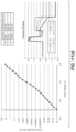
- FIG. 2 shows some typical direct tunneling current densities (gate currents) for various silicon dioxide thicknesses under different bias conditions.
- the desired high current density e.g., 5.0 amps/cm 2
- the desired high current density may be achieved in silicon dioxide for thicknesses less than 1.5 nm, even for voltages below 1.5 volts across the silicon dioxide layer.
- FIGS. 3 ( a ) and 3 ( b ) illustrate, respectively, direct tunneling of electrons into charge-trapping sublayer 112 and out of charge-trapping sublayer 112 during programming and erase operations.
- the applied programming voltage across gate electrode 114 and channel region 110 lowers the conduction bands of tunnel dielectric sublayer 111 , charge-trapping sublayer 112 and blocking dielectric sublayer 113 relative to channel region 110 .
- the lowest energy levels in the conduction band of charge-trapping sublayer 112 is lowered to slightly below that of channel region 110 to allow electrons with energy at the lowest energy levels of the conduction band in channel region 110 to direct-tunnel into charge-trapping sublayer 112 , as illustrated by arrow 301 in FIG. 3 ( a ) .
- the applied erase voltage across gate electrode 114 and channel region 110 raises the lowest energy levels in the conduction bands of tunnel dielectric sublayer 111 , charge-trapping sublayer 112 and blocking dielectric sublayer 113 relative to those of channel region 110 .
- the electric field imparts energy to electrons at the allowed energy levels of the charge-trapping sites in charge-trapping sublayer 112 to direct tunnel into channel region 110 , as illustrated by arrow 302 in FIG. 3 ( b ) .
- FIGS. 3 ( a ) and 3 ( b ) allow fast programming and erase. In contrast, erasing by holes is a slow mechanism.
- a floating-substrate quasi-volatile storage cell e.g., Harari's thin-film storage transistor
- holes in channel region 110 are insufficient to provide an adequate hole current into charge-trapping sublayer 112 ; the likely erase mechanism for such a storage transistor pulls electrons out from charge-trapping sublayer 112 .
- the voltage difference between the threshold voltages of the storage transistor in the erased state and in the programmed state is referred to as the “programming window.”
- the programming window narrows or closes with the number of cycles the storage transistor has been programmed and erased. Such programming window narrowing is due to, for example, degradation at the interface between channel region 110 and tunnel dielectric 111 , as a result of interface states formation. Programming window narrowing may also result from charge-trapping at other material interfaces, e.g., between charge-trapping sublayer 112 and blocking dielectric sublayer 113 .
- the endurance of a storage transistor refers to the number of program-erase cycles before the storage transistor fails to maintain an acceptable programming window. As illustrated in FIG.
- electrons that direct tunnel from channel region 110 to charge-trapping sublayer 112 have low energy entering charge-trapping sublayer 112 , so that they give up only a small amount of energy settling in the lowest allowed energy states in charge-trapping sublayer 112 (i.e., the lowest energy levels in the conduction bands of channel region 110 and charge-trapping sublayer 112 are very close in the presence of the programming voltage). This energy loss does not cause any appreciable damage to charge-trapping sublayer 112 .
- the energy loss by electrons entering channel region 110 during an erase operation is significantly larger.
- hot holes energetic holes
- the greater energy loss generates energetic holes (“hot holes”) in channel region 110 , which would be driven by the electric field of the erase voltage towards gate electrode 114 .
- These hot holes create interface traps at the interface between channel region 110 and tunnel dielectric sublayer 111 .
- These interface traps are detrimental to the endurance of the storage transistor and, in fact, may be primarily responsible for the programming window closing.
- the hot holes phenomenon known as the “anode hot hole injection mechanism,” provides one model for dielectric breakdown.
- FIG. 4 illustrates the evolution of the programming window in a storage transistor over more than 10 9 program and erase cycles, showing program state threshold voltage 401 and erase state threshold voltage 402 .
- a storage transistor has a tunnel dielectric layer and a charge-trapping layer between a channel region and a gate electrode, wherein the charge-tapping layer has a conduction band offset—relative to a n-type silicon conduction band—that is less than the lowering of the tunneling barrier in the tunnel dielectric layer when a programming voltage is applied, such that electrons direct tunnel into the charge-trapping layer.
- the conduction band offset of the charge-trapping layer is selected to have a value between ⁇ 1.0 eV and 2.3 eV.
- the charge-tapping layer may include one or more of: hafnium oxide (HfO 2 ), yttrium oxide (Y 2 O 3 ), silicon nitride (Si 3 N 4 ), zirconium oxide (ZrO 2 ), zirconium silicon oxide (ZrSiO 4 ), lanthanum oxide (La 2 O 3 ) tantalum oxide (Ta 2 O 5 ), cerium oxide (CeO 2 ), titanium oxide (TiO 2 ), strontium titanium oxide (SrTiO 3 ), other semiconductors, and metal nanodots (e.g., silicon, ruthenium, platinum and cobalt nanodots).
- hafnium oxide HfO 2
- Y 2 O 3 silicon nitride
- ZrO 2 zirconium oxide
- ZrSiO 4 zirconium silicon oxide
- lanthanum oxide La 2 O 3
- tantalum oxide Ta 2 O 5
- CeO 2 cerium oxide
- the storage transistor may further include a barrier layer between the tunnel dielectric layer and the charge-trapping layer, the barrier layer having a conduction band offset less than the conduction band offset of the charge-trapping layer.
- the barrier layer may also include a material having a conduction band offset between ⁇ 1.0 eV and 2.3 eV, preferably between ⁇ 1.0 eV to 1.5 eV, such as one or more of: hafnium oxide (HfO 2 ), yttrium oxide (Y 2 O 3 ), silicon nitride (Si 3 N 4 ), zirconium oxide (ZrO 2 ), zirconium silicon oxide (ZrSiO 4 ), tantalum oxide (Ta 2 O 5 ), cerium oxide (CeO 2 ), titanium oxide (TiO 2 ), strontium titanium oxide (SrTiO 3 ), other semiconductors, and metal nanodots (e.g., silicon, ruthenium, platinum and cobalt nanodots
- the tunnel dielectric layer may be as thin as 5-40 ⁇ and may be formed out of silicon oxide (e.g., SiO 2 ) or silicon nitride (SiN).
- a silicon oxide tunnel dielectric layer may be formed using conventional oxidation techniques (e.g., a high-temperature oxidation), chemical synthesis (e.g., atomic layer deposition (ALD)), or any suitable combination of these techniques.
- a reactive O 2 process may include ozone for a precisely controlled thickness and an improved oxide quality (e.g., reduced leakage due to defect sites).
- a silicon nitride tunnel dielectric layer may be formed using conventional nitridation, direct synthesis, chemical synthesis (e.g., by atomic layer deposition), or any suitable combination of these techniques.
- a plasma process may be used for a precisely controlled thickness and an improved dielectric quality (e.g., reduced leakage due to defect sites).
- the tunnel dielectric layer may also include in addition a thin aluminum oxide (Al 2 O 3 ) layer (e.g., 10 ⁇ or less).
- Al 2 O 3 aluminum oxide
- the aluminum oxide layer in the tunnel dielectric layer may be synthesized in the amorphous phase, to reduce leakage due to defect sites.
- FIG. 1 is an energy band diagram of a conventional storage transistor, which includes multiple sublayers of dielectric materials and stores charge between a channel region and a gate electrode.
- FIG. 2 shows some typical direct tunneling current densities (gate currents) for various silicon dioxide thicknesses under different bias conditions.
- FIGS. 3 ( a ) and 3 ( b ) illustrate, respectively, direct tunneling of electrons into charge-trapping sublayer 112 and out of charge-trapping sublayer 112 during programming and erase operations.
- FIG. 4 illustrates an evolution of the programming window in a storage transistor over more than 10 9 program and erase cycles, showing program state threshold voltage 401 and erase state threshold voltage 402 .
- FIG. 5 is an energy band diagram in an exemplary storage transistor having channel region 501 , tunnel dielectric layer 502 and charge-trapping layer 503 .
- FIGS. 6 ( a ), 6 ( b ) and 6 ( c ) show, respectively, (i) the lowest energy levels of the conduction bands at substrate 501 , tunnel dielectric 502 and charge-trapping layer 503 of a storage transistor; (ii) the lowest energy levels in the conduction bands of these layers of the storage transistor without application of a voltage; and (iii) the electron energy offset 515 between substrate 501 and charge-trapping layer 503 , when an erase voltage is applied.
- FIGS. 7 ( a ), 7 ( b ) and 7 ( c ) show, respectively, (i) the relative conduction band offsets at substrate 601 , tunnel dielectric 602 , low conduction band offset (LCBO) barrier layer 603 , and charge-trapping layer 604 of a storage transistor; (ii) an energy band diagram of these layers of the storage transistor without application of a voltage; and (iii) electron energy offset 615 between substrate 601 and charge-trapping layer 604 , when an erase voltage is applied.
- LCBO low conduction band offset
- FIGS. 8 ( a ), 8 ( b ) and ( c ) illustrate the conduction band offset parameters for dielectric layers 602 - 604 illustrated in FIGS. 7 ( a )- 7 ( c ) .
- FIG. 9 ( a ) illustrates direct tunneling and FIGS. 9 ( b ) and 9 ( c ) illustrate MFN tunneling in the storage transistor of FIGS. 7 ( a )- 7 ( c ) .
- FIGS. 11 ( a ), 11 ( b ), 11 ( c ) and 11 ( d ) show various simulation results for storage transistors of the present invention.
- FIG. 12 ( a ) is an energy band diagram for the conduction band of a gate stack of a storage transistor during an erase operation.
- FIG. 12 ( b ) is an energy band diagram for the conduction band of a gate stack of a storage transistor during an erase operation, the storage transistor having additional aluminum oxide layer 607 in blocking dielectric layer 610 , according to one embodiment of the present invention
- the present invention improves endurance in a storage transistor to exceed 10 11 program-erase cycles using a device structure that ensures electrons tunneling out of a charge-trapping layer into the channel region of the storage transistor (e.g., during an erase operation) are within a desirable low energy range (“cool electrons”), such that any resulting hole generations are also low-energy and are thus less damaging to the programming window.
- the device structure provides a substantial direct tunneling programming current density exceeding 1.0 amps/cm 2 (e.g., 5.0 amps/cm 2 ).
- the present invention is particularly advantageous for use in storage layers of thin-film storage transistors that are formed in 3-dimensional memory structures, such as those quasi-volatile storage transistors in the 3-dimensional arrays of NOR memory strings disclosed in Harari discussed above.
- FIG. 5 One embodiment of the present invention is illustrated by the model of FIG. 5 , showing the conduction and valence energy band boundaries 511 and 512 of an exemplary storage transistor having channel region 501 , tunnel dielectric layer 502 and charge-trapping layer 503 .
- arrow 514 represents electrons direct tunnel from charge-trapping layer 503 to channel region 501 .
- the present invention may be achieved by judiciously selecting a combination of materials for a tunnel dielectric material and a charge-trapping dielectric material, to obtain desirable conduction band offsets at these layers relative to the semiconductor substrate (i.e., the channel region) of the storage transistor.
- FIG. 6 ( a ) shows the lowest energy levels of the conduction bands at substrate 501 , tunnel dielectric 502 and charge-trapping layer 503 of the storage transistor.
- FIG. 6 ( b ) shows the lowest energy levels in the conduction bands of these layers of the storage transistor without application of a voltage.
- FIG. 6 ( c ) shows the electron energy offset 515 between substrate 501 and charge-trapping layer 503 , when an erase voltage is applied.
- Electron energy offset 515 depends on conduction band offsets between substrate 501 and each of tunnel dielectric layer 502 and charge-trapping layer 503 , as well as on the voltage applied for the erase operation. As illustrated in FIG. 6 ( c ) , for tunnel dielectric layer 502 , using different charge-trapping materials as charge-trapping layer 503 , with different conduction band offsets relative to the substrate layer 501 , results in greater or lesser energy loss in the tunneling electrons reaching substrate 501 . Likewise, for charge-trapping layer 503 , using different tunnel dielectric materials as tunnel dielectric layer 502 , with different conduction band offsets relative to the substrate layer 501 , also results in greater or lesser energy loss in the tunneling electrons reaching substrate 501 .
- Tunnel dielectric layer 502 may be as thin as 5-40 ⁇ and may be formed out of silicon oxide (e.g., SiO 2 ), silicon nitride (SiN), or silicon oxynitride (SiON).
- a silicon oxide tunnel dielectric layer may be formed using conventional oxidation techniques (e.g., a high-temperature oxidation), chemical synthesis (e.g., atomic layer deposition (ALD)), or any suitable combination of these techniques.
- a reactive O 2 process may include an ozone step (e.g., using pulsed ozone) for a precisely controlled thickness and an improved oxide quality (e.g., reduced leakage due to defect sites).
- the ozone step augments solidification of the oxide in a conformal manner, which is particularly advantageous for three-dimensional transistor structures.
- An annealing step e.g., an H 2 anneal, a NH 3 anneal, or a rapid thermal annealing
- a silicon nitride tunnel dielectric layer may be formed using conventional nitridation, direct synthesis, chemical synthesis (e.g., by ALD), or any suitable combination of these techniques.
- a plasma process may be used for a precisely controlled thickness and an improved dielectric quality (e.g., reduced leakage due to defect sites).
- Tunnel dielectric layer 502 may also include an additional thin aluminum oxide (Al 2 O 3 ) layer (e.g., 10 ⁇ or less). This additional aluminum oxide layer in the tunnel dielectric layer may be synthesized in the amorphous phase, to reduce leakage due to defect sites.
- Al 2 O 3 additional thin aluminum oxide
- tunnel dielectric layer 502 and charge-trapping layer 503 The following materials may be used to provide tunnel dielectric layer 502 and charge-trapping layer 503 :
- Using a lower conduction band offset in the charge-trapping layer provides an effective increase in tunneling barrier in the tunnel dielectric layer, resulting in improved data retention.
- FIGS. 7 ( a )- 7 ( c ) are band diagrams representative of such a structure.
- FIG. 7 ( a ) shows the relative conduction band offsets at substrate 601 , tunnel dielectric 602 , low conduction band offset barrier dielectric 603 and charge-trapping layer 604 of the storage transistor.
- FIG. 7 ( b ) is an energy band diagram of these layers of the storage transistor without application of a voltage.
- FIG. 7 ( c ) shows the electron energy offset 615 between substrate 601 and charge-trapping layer 604 , when an erase voltage is applied.
- Electron energy offset 615 depends on conduction band offsets between substrate 601 and each of tunnel dielectric layer 602 , low conduction band offset barrier layer 603 and charge-trapping layer 604 , as well as on the voltage applied for the erase operation.
- low conduction band offset (LCBO) barrier dielectric 603 preferably has a conduction band offset relative to substrate 601 that is lower than those of both tunnel dielectric layer 602 and charge-trapping layer 604 .
- LCBO barrier dielectric 603 preferably has a conduction band offset relative to substrate 601 that is lower than those of both tunnel dielectric layer 602 and charge-trapping layer 604 .
- cool electron direct tunneling may be achieved for both program and erase operations, resulting in a high endurance in the storage transistor.
- FIGS. 8 ( a )-( c ) illustrate the conduction band offset parameters for dielectric layers 602 - 604 illustrated in FIGS. 7 ( a )- 7 ( c ) .
- parameter B represents the conduction band offset of tunnel dielectric layer 602 relative to substrate 601
- parameter a represents the conduction band offset of LCBO barrier layer 603 relative to the conduction band offset of tunnel dielectric layer 602
- parameter d represents the conduction band offset of LCBO barrier layer 603 relative to substrate 601
- parameter c represents the conduction band offset of charge-trapping layer 604 relative to substrate 601 .
- the conduction band offset of LCBO barrier layer 603 should not be greater than the conduction band offset of charge-trapping layer 604 (i.e., d ⁇ c) to allow a substantial direct tunneling programming current density exceeding 1.0 amps/cm 2 (e.g., 5.0 amps/cm 2 ).
- FIG. 8 ( b ) shows sloping of the energy level at the bottom of the conduction band of tunnel dielectric layer 602 as a result of the programming voltage.
- the sloping lowers the energy level of tunnel dielectric layer 602 by parameter b over the thickness of tunnel dielectric layer 602 .
- the value of parameter b should be greater or equal to the value of parameter c (i.e., b ⁇ c).
- the value of parameter b (in eV units) is the product of the voltage drop across tunnel dielectric layer 602 and the electron charge q (i.e., 1.6 ⁇ 10 ⁇ 19 coulombs).
- the tunneling barrier becomes wider, as at least a part of LCBO barrier layer 603 remains a tunneling barrier.
- direct tunneling may give way to a modified Fowler-Nordheim (MFN) mechanism, which provides a much smaller current than direct tunneling (e.g., less than 0.1 amps/cm 2 ).
- MFN Fowler-Nordheim
- FIG. 9 ( a ) illustrates direct tunneling, under application of a programming voltage
- FIGS. 9 ( b ) and 9 ( c ) illustrate MFN tunneling, under a lower voltage (“intermediate”) and an even lower voltage, respectively, in the storage transistor of FIGS. 7 ( a )- 7 ( c )
- MFN tunneling may occur in a region of low voltage disturbs during operations of the storage transistor.
- this MFN tunneling current can be very low for a range of voltages applied.
- the materials and the thicknesses for charge-trapping layer 604 and barrier layer 603 are selected such that read disturb voltages, programming inhibit voltages or erase inhibit voltages fall within the range of low or intermediate voltages that restrict tunneling to the MFN mechanism.
- the storage transistor of the present invention provides an important advantage: high currents at the programming voltage due to direct tunneling, while having merely a low MFN tunneling current when exposed to a low voltage.
- This characteristic reduces disturbs during read, programming inhibit, or erase inhibit operations and improves data retention and endurance, particularly in quasi-volatile storage transistors of the present invention that use direct tunneling for fast programming and fast erase operations.
- LCBO barrier layer 603 improves endurance by enabling cool electron-erase operations, which reduces device degradation, as the resulting holes generated in the channel region are low-energy.
- LCBO barrier layer 603 By restricting tunneling at low voltages to MFN tunneling, LCBO barrier layer 603 also improve data retention and reduces read disturb, programming-inhibit disturbs and erase-inhibit disturbs, as the read disturbs, programming-inhibit disturbs and erase-inhibit disturbs all occur at low voltages. For example, programming-inhibit disturbs and erase-inhibit disturbs occur at half-select or a lower voltage than that used in the respective programming and erase operations. All these benefits accrue in the storage transistors biased at low voltages, while at the same time maintaining the advantages of the high efficiency of direct tunneling accrue in the storage transistors biased at the higher read, programming or erase voltages.
- FIG. 8 ( c ) shows sloping of the energy level at the bottom of the conduction band of tunnel dielectric layer 602 during an erase operation.
- the sloping raises the energy level of tunnel dielectric layer 602 by parameter b′ over the thickness of tunnel dielectric layer 602 .
- the conduction band offset of charge-trapping layer 604 should be greater than the amount by which the energy level of a charge-trapping site is below the conduction band of charge-trapping layer 604 in order for the electrons at the charge-trapping site to be included in the direct tunneling current.
- substrate 601 may be implemented by a P-doped silicon
- another 4-nm thick SiO 2 layer may be used to provide a blocking dielectric layer.
- Gate electrode 606 may be implemented by a highly-doped P-type polysilicon.
- b 1 eV
- b′ 1 eV
- an electron reaching substrate 601 by direct tunneling loses about 1.4 eV of energy during the erase operation. Scattering in LCBO barrier layer 603 , as indicated by arrow 1002 , may further reduce this energy loss.
- silicon-rich silicon nitride includes silicon as impurity, which reduces silicon nitride's band gap from 4.6 eV to about 3.6 eV for silicon-rich silicon nitride. Also, silicon nitride has a refractive index of 2.0, while silicon-rich silicon nitride has a refractive index in the range of 2.1-2.3.
- substrate 601 may be implemented by a P-doped silicon
- another 5-nm thick SiO 2 layer may be used to provide a blocking dielectric layer.
- Gate electrode 606 may be implemented by a highly-doped P-type polysilicon.
- FIG. 11 ( a )- 11 ( d ) show various simulation results for storage transistors of the present invention.
- FIG. 11 ( a ) shows a simulation of a storage transistor having a 0.8 nm thick silicon oxide tunneling dielectric layer, a 2.0 nm thick zirconium oxide LCBO barrier layer and a 5.0 nm thick silicon-rich silicon nitride trapping layer.
- FIG. 11 ( a ) shows that a direct-tunneling current density exceeding 1.0 amps/cm 2 is achieved with a programming voltage around 3.1 volts.
- FIG. 11 ( b ) shows a simulation of a storage transistor having a 1.0 nm thick silicon oxide tunneling dielectric layer, a 2.0 nm thick cerium oxide LCBO barrier layer and a 4.0 nm thick silicon-rich silicon nitride trapping layer.
- FIG. 11 ( b ) shows that a direct-tunneling current density exceeding 1.0 amps/cm 2 is achieved with a programming voltage around 1.6 volts.
- FIG. 11 ( c ) shows a simulation of a storage transistor having a 1.0 nm thick silicon oxide tunneling dielectric layer, a 2.0 nm thick tantalum oxide LCBO barrier layer and a 4.0 nm thick silicon-rich silicon nitride trapping layer.
- FIG. 11 ( c ) shows that a direct-tunneling current density exceeding 1.0 amps/cm 2 is achieved with a programming voltage around 1.8 volts.
- FIG. 11 ( d ) shows a simulation of a storage transistor having a 1.0 nm thick silicon nitride tunneling dielectric layer, a 2.0 nm thick cerium oxide LCBO barrier layer and a 4.0 nm thick silicon-rich silicon nitride trapping layer.
- FIG. 11 ( d ) shows that a direct-tunneling current density exceeding 1.0 amps/cm 2 is achieved with a programming voltage around 2.1 volts.
- FIG. 12 ( a ) illustrates a “reverse injection electrons” phenomenon that may occur during an erase operation.
- the reverse injection electrons may affect endurance adversely.
- FIG. 12 ( a ) is an energy band diagram for the conduction band of a gate stack in a storage transistor during an erase operation.
- the gate stack includes substrate 601 , tunnel dielectric 602 , LCBO barrier dielectric 603 , charge-trapping layer 604 , blocking dielectric layer 605 and gate electrode 606 .
- Blocking dielectric layer 605 may be, for example, silicon oxide (SiO 2 )).
- the relatively high electric field across blocking dielectric layer 605 may cause high-energy electrons—indicated in FIG. 12 ( a ) by arrow 1201 —to tunnel from the gate electrode into charge-trapping layer 604 , or even into tunnel dielectric layer 602 .
- These reverse injection electrons may damage these layers, adversely affecting the storage transistor's endurance.
- reverse injection electrons may be significantly reduced or substantially eliminating by including a layer of material with a high dielectric constant (“high-k material”), such as aluminum oxide (Al 2 O 3 ) in the blocking dielectric layer (e.g., blocking dielectric layer 605 of FIG. 10 ( a ) ).
- high-k material such as aluminum oxide (Al 2 O 3 )
- Al 2 O 3 aluminum oxide
- a high work function metal e.g., greater than 3.8 eV, preferably not less than 4.0 eV
- a high-k material of t H provides an equivalent oxide thickness t EOT given by:
- t E ⁇ O ⁇ T t H ⁇ ⁇ ox ⁇ H
- ⁇ ox and ⁇ H are the relative dielectric constants of silicon oxide and the high-k material, respectively.
- a high-k material can provide the same desirable transistor characteristics (e.g., gate capacitance) at a thickness of t H , without incurring undesirable leakage of its silicon oxide layer counterpart at the much thinner equivalent thickness t EOT .
- FIG. 12 ( b ) is an energy band diagram for the conduction band of a gate stack in a storage transistor during an erase operation, the storage transistor having additional aluminum oxide layer 607 in blocking dielectric layer 610 , according to one embodiment of the present invention.
- blocking dielectric layer 610 includes aluminum oxide layer 607 and silicon oxide layer 608 .
- blocking dielectric layer 610 has an equivalent oxide thickness that is substantially the same as blocking layer dielectric 605 of FIG. 12 ( a ) .
- aluminum oxide has a relative dielectric constant of 9.0
- silicon oxide's relative dielectric constant is 3.9, the actual combined physical thickness of aluminum oxide 607 and silicon oxide 608 in FIG.
- a high work function metal is preferred for gate electrode 606 .
- the high work function metal creates a high barrier (indicated by barrier height 1202 in FIG. 12 ( b ) ) at the gate electrode-aluminum oxide interface, which significantly reduces reverse electron injection the erase operation.
- Suitable high work function metals include: tungsten (W), tantalum nitride (TaN), tantalum silicon nitride (TaSiN).
Landscapes
- Non-Volatile Memory (AREA)
- Semiconductor Memories (AREA)
- Thin Film Transistor (AREA)
Abstract
Description
| Material | Conduction Band Offset | ||
| Silicon oxide (SiO2) | 3.15 | eV | ||
| Hafnium oxide (HfO2) | 1.5 | eV | ||
| Silicon Nitride (Si3N4) | 2.4 | eV | ||
| Yttrium oxide (Y2O3) | 2.3 | eV | ||
| Zirconium oxide (ZrO2) | 1.4 | eV | ||
| Zirconium silicon oxide (ZrSiO4) | 1; 5 | eV | ||
| Lanthanum oxide (La2O3) | 2.3 | eV | ||
| Silicon oxinitrides (SiN:H) | 1.3-2.4 | eV | ||
| Tantalum oxide (Ta2O5) | 0.3 | eV | ||
| Cerium oxide (CeO2) | 0.6 | eV | ||
| Titanium oxide (TiO2) | 0.0 | eV | ||
| Strontium titanium oxide (SrTiO3) | 0.0 | eV | ||
| Silicon-rich silicon nitride (SiN:Si) | 1.35 | eV | ||
| Silicon nanodots | 0.0 | eV | ||
| Ruthenium nanodots | 0.7 | eV | ||
| Cobalt nanodots | 1.0 | eV | ||
where κox and κH are the relative dielectric constants of silicon oxide and the high-k material, respectively. Thus, a high-k material can provide the same desirable transistor characteristics (e.g., gate capacitance) at a thickness of tH, without incurring undesirable leakage of its silicon oxide layer counterpart at the much thinner equivalent thickness tEOT.
Claims (33)
Priority Applications (1)
| Application Number | Priority Date | Filing Date | Title |
|---|---|---|---|
| US18/046,433 US12183834B2 (en) | 2020-01-22 | 2022-10-13 | Cool electron erasing in thin-film storage transistors |
Applications Claiming Priority (4)
| Application Number | Priority Date | Filing Date | Title |
|---|---|---|---|
| US202062964472P | 2020-01-22 | 2020-01-22 | |
| US202062992754P | 2020-03-20 | 2020-03-20 | |
| US17/155,673 US11515432B2 (en) | 2020-01-22 | 2021-01-22 | Cool electron erasing in thin-film storage transistors |
| US18/046,433 US12183834B2 (en) | 2020-01-22 | 2022-10-13 | Cool electron erasing in thin-film storage transistors |
Related Parent Applications (1)
| Application Number | Title | Priority Date | Filing Date |
|---|---|---|---|
| US17/155,673 Continuation US11515432B2 (en) | 2020-01-22 | 2021-01-22 | Cool electron erasing in thin-film storage transistors |
Publications (2)
| Publication Number | Publication Date |
|---|---|
| US20230065451A1 US20230065451A1 (en) | 2023-03-02 |
| US12183834B2 true US12183834B2 (en) | 2024-12-31 |
Family
ID=76857256
Family Applications (2)
| Application Number | Title | Priority Date | Filing Date |
|---|---|---|---|
| US17/155,673 Active US11515432B2 (en) | 2020-01-22 | 2021-01-22 | Cool electron erasing in thin-film storage transistors |
| US18/046,433 Active 2041-03-14 US12183834B2 (en) | 2020-01-22 | 2022-10-13 | Cool electron erasing in thin-film storage transistors |
Family Applications Before (1)
| Application Number | Title | Priority Date | Filing Date |
|---|---|---|---|
| US17/155,673 Active US11515432B2 (en) | 2020-01-22 | 2021-01-22 | Cool electron erasing in thin-film storage transistors |
Country Status (4)
| Country | Link |
|---|---|
| US (2) | US11515432B2 (en) |
| CN (1) | CN114846551A (en) |
| TW (1) | TWI767512B (en) |
| WO (1) | WO2021150879A1 (en) |
Families Citing this family (2)
| Publication number | Priority date | Publication date | Assignee | Title |
|---|---|---|---|---|
| KR102719982B1 (en) * | 2017-06-20 | 2024-10-22 | 선라이즈 메모리 코포레이션 | 3D NOR memory array architecture and its manufacturing method |
| US11984513B2 (en) * | 2020-10-14 | 2024-05-14 | Korea Advanced Institute Of Science And Technology | Charge trapping non-volatile organic memory device |
Citations (259)
| Publication number | Priority date | Publication date | Assignee | Title |
|---|---|---|---|---|
| US4213139A (en) | 1978-05-18 | 1980-07-15 | Texas Instruments Incorporated | Double level polysilicon series transistor cell |
| US5583808A (en) | 1994-09-16 | 1996-12-10 | National Semiconductor Corporation | EPROM array segmented for high performance and method for controlling same |
| US5646886A (en) | 1995-05-24 | 1997-07-08 | National Semiconductor Corporation | Flash memory having segmented array for improved operation |
| US5656842A (en) | 1995-06-20 | 1997-08-12 | Mitsubishi Denki Kabushiki Kaisha | Vertical mosfet including a back gate electrode |
| US5768192A (en) | 1996-07-23 | 1998-06-16 | Saifun Semiconductors, Ltd. | Non-volatile semiconductor memory cell utilizing asymmetrical charge trapping |
| US5789776A (en) | 1995-09-22 | 1998-08-04 | Nvx Corporation | Single poly memory cell and array |
| US5880993A (en) | 1996-09-30 | 1999-03-09 | Sgs-Thomson Microelectronics, S.R.L. | Method and circuit for checking multilevel programming of floating-gate nonvolatile memory cells particularly flash cells |
| US5915167A (en) | 1997-04-04 | 1999-06-22 | Elm Technology Corporation | Three dimensional structure memory |
| US6040605A (en) | 1998-01-28 | 2000-03-21 | Hitachi, Ltd. | Semiconductor memory device |
| US6107133A (en) | 1998-05-28 | 2000-08-22 | International Business Machines Corporation | Method for making a five square vertical DRAM cell |
| US6118171A (en) | 1998-12-21 | 2000-09-12 | Motorola, Inc. | Semiconductor device having a pedestal structure and method of making |
| US6130838A (en) | 1997-08-12 | 2000-10-10 | Samsung Electronics, Co., Ltd. | Structure nonvolatile semiconductor memory cell array and method for fabricating same |
| US20010030340A1 (en) | 1998-11-04 | 2001-10-18 | Ichiro Fujiwara | Nonvolatile semiconductor memory device and process of production and write method thereof |
| US6313518B1 (en) | 1997-10-14 | 2001-11-06 | Micron Technology, Inc. | Porous silicon oxycarbide integrated circuit insulator |
| US6314046B1 (en) | 1999-03-30 | 2001-11-06 | Sanyo Electric Co., Ltd. | Dual memory control circuit |
| US20010053092A1 (en) | 2000-06-12 | 2001-12-20 | Sony Corporation | Memory system and programming method thereof |
| US20020012271A1 (en) | 2000-02-29 | 2002-01-31 | Leonard Forbes | Static NVRAM with ultra thin tunnel oxides |
| US20020028541A1 (en) | 2000-08-14 | 2002-03-07 | Lee Thomas H. | Dense arrays and charge storage devices, and methods for making same |
| US6362508B1 (en) | 2000-04-03 | 2002-03-26 | Tower Semiconductor Ltd. | Triple layer pre-metal dielectric structure for CMOS memory devices |
| US20020051378A1 (en) | 2000-08-17 | 2002-05-02 | Takashi Ohsawa | Semiconductor memory device and method of manufacturing the same |
| US6434053B1 (en) | 1999-12-06 | 2002-08-13 | Sony Corporation | Nonvolatile semiconductor memory device and method of operation thereof |
| US20020193484A1 (en) | 2001-02-02 | 2002-12-19 | The 54 Group, Ltd. | Polymeric resins impregnated with insect repellants |
| US20030038318A1 (en) | 2001-08-24 | 2003-02-27 | Leonard Forbes | Vertical transistor with horizontal gate layers |
| US6580124B1 (en) | 2000-08-14 | 2003-06-17 | Matrix Semiconductor Inc. | Multigate semiconductor device with vertical channel current and method of fabrication |
| US6627503B2 (en) | 2000-02-11 | 2003-09-30 | Sharp Laboratories Of America, Inc. | Method of forming a multilayer dielectric stack |
| JP2004079606A (en) | 2002-08-12 | 2004-03-11 | Fujitsu Ltd | Semiconductor device having high dielectric constant film and method of manufacturing the same |
| US6754105B1 (en) | 2003-05-06 | 2004-06-22 | Advanced Micro Devices, Inc. | Trench side wall charge trapping dielectric flash memory device |
| US6774458B2 (en) | 2002-07-23 | 2004-08-10 | Hewlett Packard Development Company, L.P. | Vertical interconnection structure and methods |
| US20040214387A1 (en) | 2002-07-08 | 2004-10-28 | Madurawe Raminda Udaya | Methods for fabricating three dimensional integrated circuits |
| US20040246807A1 (en) | 2003-06-03 | 2004-12-09 | Seung-Hoon Lee | Multi-port memory device with stacked banks |
| US20040264247A1 (en) | 2003-06-30 | 2004-12-30 | Kim Ki Seog | Method for reading flash memory cell, NAND-type flash memory apparatus, and NOR-type flash memory apparatus |
| US20040262772A1 (en) | 2003-06-30 | 2004-12-30 | Shriram Ramanathan | Methods for bonding wafers using a metal interlayer |
| US20040262681A1 (en) | 2003-05-28 | 2004-12-30 | Fujio Masuoka | Semiconductor device |
| US6873004B1 (en) | 2002-02-04 | 2005-03-29 | Nexflash Technologies, Inc. | Virtual ground single transistor memory cell, memory array incorporating same, and method of operation thereof |
| US20050128815A1 (en) | 2003-12-09 | 2005-06-16 | Renesas Technology Corp. | Semiconductor data processing device |
| US6946703B2 (en) | 2003-01-09 | 2005-09-20 | Samsung Electronics Co., Ltd. | SONOS memory device having side gate stacks and method of manufacturing the same |
| US20050280061A1 (en) | 2004-06-21 | 2005-12-22 | Sang-Yun Lee | Vertical memory device structures |
| US20060001083A1 (en) | 2001-08-30 | 2006-01-05 | Micron Technology, Inc. | Scalable Flash/NV structures and devices with extended endurance |
| US7005350B2 (en) | 2002-12-31 | 2006-02-28 | Matrix Semiconductor, Inc. | Method for fabricating programmable memory array structures incorporating series-connected transistor strings |
| JP2006099827A (en) | 2004-09-28 | 2006-04-13 | Sharp Corp | Semiconductor memory device and electronic device |
| US20060155921A1 (en) | 2004-12-16 | 2006-07-13 | Gorobets Sergey A | Non-volatile memory and method with multi-stream update tracking |
| US20060189154A1 (en) * | 2005-02-23 | 2006-08-24 | Micron Technology, Inc. | Atomic layer deposition of Hf3N4/HfO2 films as gate dielectrics |
| US20060261404A1 (en) | 2003-12-17 | 2006-11-23 | Micron Technology, Inc. | Vertical NROM NAND flash memory array |
| US20070023817A1 (en) | 2005-07-28 | 2007-02-01 | Dao Thuy B | Structure and manufacturing method of multi-gate dielectric thicknesses for planar double gate device having multi-threshold voltages |
| US20070045711A1 (en) * | 2005-09-01 | 2007-03-01 | Micron Technology, Inc. | High performance multi-level non-volatile memory |
| US7223653B2 (en) | 2004-06-15 | 2007-05-29 | International Business Machines Corporation | Process for forming a buried plate |
| US20070134876A1 (en) | 2005-12-09 | 2007-06-14 | Macronix International Co., Ltd. | Stacked thin film transistor, non-volatile memory devices and methods for fabricating the same |
| US7307308B2 (en) | 2003-04-07 | 2007-12-11 | Silicon Storage Technology, Inc. | Buried bit line non-volatile floating gate memory cell with independent controllable control gate in a trench, and array thereof, and method of formation |
| US20080032465A1 (en) * | 2006-08-03 | 2008-02-07 | Micron Technology, Inc. | Deposition of ZrAION films |
| US20080054346A1 (en) | 2006-09-01 | 2008-03-06 | Kabushiki Kaisha Toshiba | Semiconductor device |
| US20080160765A1 (en) | 2006-12-27 | 2008-07-03 | Hynix Semiconductor Inc. | Method for forming pattern in semiconductor device |
| US20080178794A1 (en) | 2007-01-25 | 2008-07-31 | Au Optronics Corporation | Methods of forming silicon nanocrystals by laser annealing |
| US20080239812A1 (en) | 2007-03-30 | 2008-10-02 | Kabushiki Kaisha Toshiba | Nonvolatile semiconductor memory system |
| US20080266960A1 (en) | 2007-04-30 | 2008-10-30 | Macronix International Co., Ltd. | Non-volatile memory and manufacturing method and operating method thereof and circuit system including the non-volatile memory |
| US20080291723A1 (en) | 2007-05-23 | 2008-11-27 | Wang Daniel C | Source biasing of nor-type flash array with dynamically variable source resistance |
| US20080301359A1 (en) | 2004-12-16 | 2008-12-04 | Peter John Smith | Non-Volatile Memory and Method With Multi-Stream Updating |
| US7465980B2 (en) | 2004-09-10 | 2008-12-16 | Fujitsu Limited | Ferroelectric memory, multivalent data recording method and multivalent data reading method |
| US7489002B2 (en) | 2001-02-09 | 2009-02-10 | Micron Technology, Inc. | Memory having a vertical transistor |
| US20090057722A1 (en) | 2007-05-30 | 2009-03-05 | Unisantis Electronics (Japan) Ltd. | Semiconductor device |
| US7524725B2 (en) | 2005-03-31 | 2009-04-28 | Hynix Semiconductor Inc. | Vertical transistor of semiconductor device and method for forming the same |
| US7542348B1 (en) | 2007-12-19 | 2009-06-02 | Juhan Kim | NOR flash memory including bipolar segment read circuit |
| US20090140318A1 (en) | 2007-12-03 | 2009-06-04 | Zhong Dong | Nonvolatile memories with higher conduction-band edge adjacent to charge-trapping dielectric |
| US20090157946A1 (en) | 2007-12-12 | 2009-06-18 | Siamak Arya | Memory having improved read capability |
| US20090237996A1 (en) | 2008-03-20 | 2009-09-24 | Micron Technology, Inc. | Memory structure having volatile and non-volatile memory portions |
| US20090268519A1 (en) | 2000-01-18 | 2009-10-29 | Tomoyuki Ishii | Semiconductor integrated circuit device and data processor device |
| US7612411B2 (en) | 2005-08-03 | 2009-11-03 | Walker Andrew J | Dual-gate device and method |
| US20090279360A1 (en) | 2008-05-07 | 2009-11-12 | Aplus Flash Technology, Inc. | NAND based NMOS NOR flash memory cell, a NAND based NMOS nor flash memory array, and a method of forming a NAND based NMOS NOR flash memory array |
| US20090290442A1 (en) | 2005-06-24 | 2009-11-26 | Rajan Suresh N | Method and circuit for configuring memory core integrated circuit dies with memory interface integrated circuit dies |
| US20090316487A1 (en) | 2008-06-20 | 2009-12-24 | Aplus Flash Technology, Inc. | Apparatus and method for inhibiting excess leakage current in unselected nonvolatile memory cells in an array |
| CN101615618A (en) | 2008-06-23 | 2009-12-30 | 三星电子株式会社 | Integrated circuit and manufacturing method thereof, solid-state memory module and computer system |
| JP2010074096A (en) * | 2008-09-22 | 2010-04-02 | Toshiba Corp | Memory cell of nonvolatile semiconductor storage device |
| US7709359B2 (en) | 2007-09-05 | 2010-05-04 | Qimonda Ag | Integrated circuit with dielectric layer |
| US20100121994A1 (en) | 2008-11-10 | 2010-05-13 | International Business Machines Corporation | Stacked memory array |
| JP2010108522A (en) | 2010-02-02 | 2010-05-13 | Toshiba Corp | Method of controlling memory system |
| US20100124116A1 (en) | 2008-11-14 | 2010-05-20 | Kabushiki Kaisha Toshiba | Non-volatile semiconductor storage device |
| US20100128509A1 (en) | 2008-11-25 | 2010-05-27 | Sukpil Kim | Three-Dimensional Semiconductor Devices and Methods of Operating the Same |
| US20100148215A1 (en) | 2007-05-14 | 2010-06-17 | Infineon Technologies Ag | IGBT Having One or More Stacked Zones Formed within a Second Layer of the IGBT |
| US20100219392A1 (en) | 2009-02-27 | 2010-09-02 | Nobuyoshi Awaya | Nonvolatile semiconductor memory device and manufacturing method for same |
| US7804145B2 (en) | 2008-03-27 | 2010-09-28 | Kabushiki Kaisha Toshiba | Semiconductor device, capacitor, and field effect transistor |
| US20100254191A1 (en) | 2009-04-01 | 2010-10-07 | Byoungkeun Son | Semiconductor memory device comprising three-dimensional memory cell array |
| JP2010251572A (en) | 2009-04-16 | 2010-11-04 | Toshiba Corp | Nonvolatile semiconductor memory device |
| US20110003418A1 (en) | 2009-07-03 | 2011-01-06 | Semiconductor Energy Laboratory Co., Ltd. | Display device including transistor and manufacturing method thereof |
| JP2011028540A (en) | 2009-07-27 | 2011-02-10 | Renesas Electronics Corp | Information processing system, method for controlling cache memory, program and compiler |
| US20110044113A1 (en) | 2009-08-18 | 2011-02-24 | Samsung Electronics Co., Ltd. | Nonvolatile memory device, method for programming same, and memory system incorporating same |
| US7898009B2 (en) | 2007-02-22 | 2011-03-01 | American Semiconductor, Inc. | Independently-double-gated transistor memory (IDGM) |
| US20110075486A1 (en) | 2009-09-28 | 2011-03-31 | Macronix International Co., Ltd. | Charge trapping memory cell having bandgap engineered tunneling structure with oxynitride isolation layer |
| US20110115011A1 (en) | 2009-11-13 | 2011-05-19 | Fujio Masuoka | Semiconductor element and semiconductor device |
| US20110134705A1 (en) | 2009-12-07 | 2011-06-09 | Stmicroelectronics (R&D) Ltd | Integrated circuit package with multiple dies and a multiplexed communications interface |
| US20110170266A1 (en) | 2010-01-08 | 2011-07-14 | Ibm Corporation | 4d device process and structure |
| US20110208905A1 (en) | 2008-12-09 | 2011-08-25 | Rambus Inc. | Non-Volatile Memory Device For Concurrent And Pipelined Memory Operations |
| US8026521B1 (en) | 2010-10-11 | 2011-09-27 | Monolithic 3D Inc. | Semiconductor device and structure |
| US20110298013A1 (en) | 2010-06-07 | 2011-12-08 | Samsung Electronics Co., Ltd. | Vertical Structure Semiconductor Memory Devices And Methods Of Manufacturing The Same |
| US20110310683A1 (en) | 2001-09-28 | 2011-12-22 | Micron Technology, Inc. | Non-volatile memory control |
| US20120063223A1 (en) | 2010-09-09 | 2012-03-15 | Aplus Flash Technology, Inc. | Most compact flotox-based combo NVM design without sacrificing EEPROM endurance cycles for 1-die data and code storage |
| US8139418B2 (en) | 2009-04-27 | 2012-03-20 | Micron Technology, Inc. | Techniques for controlling a direct injection semiconductor memory device |
| US8178396B2 (en) | 2009-03-11 | 2012-05-15 | Micron Technology, Inc. | Methods for forming three-dimensional memory devices, and related structures |
| US20120146126A1 (en) | 2007-08-27 | 2012-06-14 | Macronix International Co., Ltd. | High-k capped blocking dielectric bandgap engineered sonos and monos |
| US20120182801A1 (en) | 2011-01-19 | 2012-07-19 | Macronix International Co., Ltd. | Memory Architecture of 3D NOR Array |
| KR20120085603A (en) | 2011-01-24 | 2012-08-01 | 김진선 | Non-volatile memory device, method of operating the same, and method of fabricating the same |
| KR20120085591A (en) | 2011-01-24 | 2012-08-01 | 김진선 | Non-volatile memory device, method of operating the same, and method of fabricating the same |
| US8242504B2 (en) | 2008-07-31 | 2012-08-14 | Samsung Electronics Co., Ltd. | Oxide semiconductor and thin film transistor including the same |
| US20120243314A1 (en) | 2011-03-25 | 2012-09-27 | Kabushiki Kaisha Toshiba | Nonvolatile semiconductor memory device |
| US8278183B2 (en) | 2007-07-27 | 2012-10-02 | X-Fab Semiconductor Foundries Ag | Production of isolation trenches with different sidewall dopings |
| US8304823B2 (en) | 2008-04-21 | 2012-11-06 | Namlab Ggmbh | Integrated circuit including a ferroelectric memory cell and method of manufacturing the same |
| US20120307568A1 (en) | 2011-06-06 | 2012-12-06 | Micron Technology, Inc. | Techniques for providing a semiconductor memory device |
| US20120327714A1 (en) | 2011-06-23 | 2012-12-27 | Macronix International Co., Ltd. | Memory Architecture of 3D Array With Diode in Memory String |
| US20130031325A1 (en) | 2011-07-29 | 2013-01-31 | The Boeing Company | System for Updating an Associative Memory |
| US8383482B2 (en) | 2009-09-29 | 2013-02-26 | Samsung Electronics Co., Ltd. | Three-dimensional semiconductor memory device and method of fabricating the same |
| US8395942B2 (en) | 2010-05-17 | 2013-03-12 | Sandisk Technologies Inc. | Junctionless TFT NAND flash memory |
| US20130178031A1 (en) | 2007-05-25 | 2013-07-11 | Cypress Semiconductor Corporation | Integration of non-volatile charge trap memory devices and logic cmos devices |
| US20130256780A1 (en) | 2012-03-30 | 2013-10-03 | Kabushiki Kaisha Toshiba | Semiconductor device and manufacturing method thereof |
| US20140006688A1 (en) * | 2012-07-02 | 2014-01-02 | Super Talent Technology, Corp. | Endurance and Retention Flash Controller with Programmable Binary-Levels-Per-Cell Bits Identifying Pages or Blocks as having Triple, Multi, or Single-Level Flash-Memory Cells |
| US20140015036A1 (en) | 2012-07-13 | 2014-01-16 | United Silicon Carbide, Inc. | Trenched and implanted accumulation mode metal-oxide-semiconductor field-effect transistor |
| US20140040698A1 (en) | 2012-08-06 | 2014-02-06 | Advanced Micro Devices, Inc. | Stacked memory device with metadata mangement |
| US20140070290A1 (en) | 2012-09-10 | 2014-03-13 | Kabushiki Kaisha Toshiba | Ferroelectric memory and manufacturing method of the same |
| US20140075135A1 (en) | 2012-09-11 | 2014-03-13 | Samsung Electronics Co., Ltd. | Semiconductor memory device with operation functions |
| US20140112075A1 (en) | 2012-10-24 | 2014-04-24 | Sandisk Technologies Inc. | Pre-Charge During Programming For 3D Memory Using Gate-Induced Drain Leakage |
| US20140117366A1 (en) | 2012-10-31 | 2014-05-01 | Kabushiki Kaisha Toshiba | Semiconductor device and method for manufacturing same |
| US8743612B2 (en) | 2012-01-31 | 2014-06-03 | SK Hynix Inc. | Three-dimensional non-volatile memory device |
| US20140151774A1 (en) | 2012-12-04 | 2014-06-05 | Mosaid Technologies Incorporated | Nand flash memory with vertical cell stack structure and method for manufacturing same |
| US8767473B2 (en) | 2009-06-19 | 2014-07-01 | Samsung Electronics Co., Ltd. | Programming methods for three-dimensional memory devices having multi-bit programming, and three-dimensional memory devices programmed thereby |
| US8767436B2 (en) | 2011-02-01 | 2014-07-01 | Stmicroelectronics S.R.L. | Memory support provided with memory elements of ferroelectric material and non-destructive reading method thereof |
| US20140213032A1 (en) | 2013-01-31 | 2014-07-31 | Sandisk 3D Llc | Process For Forming Resistive Switching Memory Cells Using Nano-Particles |
| US20140229131A1 (en) | 2012-05-04 | 2014-08-14 | Lsi Corporation | Retention-drift-history-based non-volatile memory read threshold optimization |
| US20140247674A1 (en) | 2013-03-01 | 2014-09-04 | Micron Technology, Inc. | Vertical access device and apparatuses having a body connection line, and related method of operating the same |
| US8848425B2 (en) | 2008-12-19 | 2014-09-30 | Unity Semiconductor Corporation | Conductive metal oxide structures in non volatile re-writable memory devices |
| US8878278B2 (en) | 2012-03-21 | 2014-11-04 | Sandisk Technologies Inc. | Compact three dimensional vertical NAND and method of making thereof |
| US20140328128A1 (en) | 2013-05-01 | 2014-11-06 | Zeno Semiconductor, Inc. | NAND String Utilizing Floating Body Memory Cell |
| US20140340952A1 (en) | 2013-05-17 | 2014-11-20 | Micron Technology, Inc. | Apparatuses having a ferroelectric field-effect transistor memory array and related method |
| US20140355328A1 (en) | 2013-06-04 | 2014-12-04 | Namlab Ggmbh | Ferroelectric memory cell for an integrated circuit |
| US20150054507A1 (en) | 2012-11-23 | 2015-02-26 | Samsung Electronics Co., Ltd. | Method and apparatus for capturing magnetic resonance image |
| US20150098272A1 (en) | 2013-10-03 | 2015-04-09 | Apple Inc. | Programmable peak-current control in non-volatile memory devices |
| US20150113214A1 (en) | 2013-10-21 | 2015-04-23 | Sehat Sutardja | Final level cache system and corresponding methods |
| US20150155876A1 (en) | 2012-08-06 | 2015-06-04 | Advanced Micro Devices, Inc. | Die-stacked memory device with reconfigurable logic |
| US9053801B2 (en) | 2012-11-30 | 2015-06-09 | Micron Technology, Inc. | Memory cells having ferroelectric materials |
| US20150194440A1 (en) | 2014-01-09 | 2015-07-09 | Young-Jin Noh | Nonvolatile Memory Devices And Methods Of Fabricating The Same |
| US20150249143A1 (en) | 2014-02-28 | 2015-09-03 | Sandisk 3D Llc | Method For Forming Oxide Below Control Gate In Vertical Channel Thin Film Transistor |
| US20150263005A1 (en) | 2013-07-10 | 2015-09-17 | Galaxycore Shanghai Limited Corporation | Dynamic Random Access Memory (DRAM) and Production Method, Semiconductor Packaging Component and Packaging Method |
| US9190293B2 (en) | 2013-12-18 | 2015-11-17 | Applied Materials, Inc. | Even tungsten etch for high aspect ratio trenches |
| US9202694B2 (en) | 2013-03-04 | 2015-12-01 | Sandisk 3D Llc | Vertical bit line non-volatile memory systems and methods of fabrication |
| US9219225B2 (en) | 2013-10-31 | 2015-12-22 | Micron Technology, Inc. | Multi-bit ferroelectric memory device and methods of forming the same |
| US20150372099A1 (en) | 2014-06-19 | 2015-12-24 | Taiwan Semiconductor Manufacturing Company, Ltd. | Contact silicide formation using a spike annealing process |
| US9230985B1 (en) | 2014-10-15 | 2016-01-05 | Sandisk 3D Llc | Vertical TFT with tunnel barrier |
| US9231206B2 (en) | 2013-09-13 | 2016-01-05 | Micron Technology, Inc. | Methods of forming a ferroelectric memory cell |
| US20160013156A1 (en) | 2014-07-14 | 2016-01-14 | Apple Inc. | Package-on-package options with multiple layer 3-d stacking |
| US20160019951A1 (en) | 2014-07-18 | 2016-01-21 | Samsung Electronics Co., Ltd. | Resistive memory device, resistive memory system, and method of operating resistive memory device |
| US20160035711A1 (en) | 2014-07-29 | 2016-02-04 | Dyi-chung Hu | Stacked package-on-package memory devices |
| US9263577B2 (en) | 2014-04-24 | 2016-02-16 | Micron Technology, Inc. | Ferroelectric field effect transistors, pluralities of ferroelectric field effect transistors arrayed in row lines and column lines, and methods of forming a plurality of ferroelectric field effect transistors |
| US20160086970A1 (en) | 2014-09-23 | 2016-03-24 | Haibing Peng | Three-dimensional non-volatile nor-type flash memory |
| US20160118404A1 (en) | 2014-10-09 | 2016-04-28 | Haibing Peng | Three-dimensional non-volatile ferroelectric random access memory |
| US9337210B2 (en) | 2013-08-12 | 2016-05-10 | Micron Technology, Inc. | Vertical ferroelectric field effect transistor constructions, constructions comprising a pair of vertical ferroelectric field effect transistors, vertical strings of ferroelectric field effect transistors, and vertical strings of laterally opposing pairs of vertical ferroelectric field effect transistors |
| US20160141294A1 (en) | 2014-11-13 | 2016-05-19 | Sandisk Technologies Inc. | Three-dimensional memory structure with multi-component contact via structure and method of making thereof |
| US9391084B2 (en) | 2014-06-19 | 2016-07-12 | Macronix International Co., Ltd. | Bandgap-engineered memory with multiple charge trapping layers storing charge |
| US9412752B1 (en) | 2015-09-22 | 2016-08-09 | Macronix International Co., Ltd. | Reference line and bit line structure for 3D memory |
| US9443861B1 (en) | 2015-05-28 | 2016-09-13 | Sandisk Technologies Llc | Fluorine-blocking insulating spacer for backside contact structure of three-dimensional memory structures |
| US20160276360A1 (en) | 2015-03-17 | 2016-09-22 | Sandisk Technologies Inc. | Honeycomb cell structure three-dimensional non-volatile memory device |
| US9455268B2 (en) | 2014-02-13 | 2016-09-27 | Samsung Electronics Co., Ltd. | Staircase-shaped connection structures of three-dimensional semiconductor devices |
| US20160300724A1 (en) | 2007-05-25 | 2016-10-13 | Cypress Semiconductor Corporation | Oxide-Nitride-Oxide Stack Having Multiple Oxynitride Layers |
| US9472560B2 (en) | 2014-06-16 | 2016-10-18 | Micron Technology, Inc. | Memory cell and an array of memory cells |
| US20160314042A1 (en) | 2015-04-27 | 2016-10-27 | Invensas Corporation | Preferred state encoding in non-volatile memories |
| US9558804B2 (en) | 2014-07-23 | 2017-01-31 | Namlab Ggmbh | Charge storage ferroelectric memory hybrid and erase scheme |
| US20170053906A1 (en) | 2015-08-23 | 2017-02-23 | Monolithic 3D Inc. | Semiconductor memory device and structure |
| US20170062456A1 (en) | 2015-08-31 | 2017-03-02 | Cypress Semiconductor Corporation | Vertical division of three-dimensional memory device |
| US20170092370A1 (en) | 2015-09-30 | 2017-03-30 | Eli Harari | Multi-gate nor flash thin-film transistor strings arranged in stacked horizontal active strips with vertical control gates |
| US20170092371A1 (en) * | 2015-09-30 | 2017-03-30 | Eli Harari | Capacitive-coupled non-volatile thin-film transistor strings in three dimensional arrays |
| US9620605B2 (en) | 2015-05-15 | 2017-04-11 | Taiwan Semiconductor Manufacturing Company, Ltd. | Semiconductor device structure and method |
| US9633944B2 (en) | 2015-04-28 | 2017-04-25 | SK Hynix Inc. | Semiconductor device and manufacturing method thereof |
| US20170140807A1 (en) | 2014-07-03 | 2017-05-18 | Yale University | Circuitry for Ferroelectric FET-Based Dynamic Random Access Memory and Non-Violatile Memory |
| US20170148517A1 (en) | 2015-11-25 | 2017-05-25 | Eli Harari | Three-dimensional vertical nor flash thin film transistor strings |
| US20170148810A1 (en) | 2015-11-20 | 2017-05-25 | Sandisk Technologies Llc | Three-dimensional nand device containing support pedestal structures for a buried source line and method of making the same |
| US9711529B2 (en) | 2015-05-05 | 2017-07-18 | Semiconductor Manufacturing International (Shanghai) Corporation | 3D NAND device and fabrication method thereof |
| US20170213821A1 (en) | 2014-08-26 | 2017-07-27 | Monolithic 3D Inc. | 3d semiconductor device and structure |
| US9748172B2 (en) | 2015-02-25 | 2017-08-29 | Sandisk Technologies Llc | Floating staircase word lines and process in a 3D non-volatile memory having vertical bit lines |
| US9799761B2 (en) | 2013-03-11 | 2017-10-24 | Monolithic 3D Inc. | 3DIC based system with memory cells and transistors |
| US9818848B2 (en) | 2015-04-29 | 2017-11-14 | Yale University | Three-dimensional ferroelectric FET-based structures |
| US9830969B2 (en) | 2015-12-03 | 2017-11-28 | Namlab Ggmbh | Multilevel ferroelectric memory cell for an integrated circuit |
| US20170358594A1 (en) | 2016-06-13 | 2017-12-14 | Sandisk Technologies Llc | Method of forming a staircase in a semiconductor device using a linear alignmnent control feature |
| US20180006044A1 (en) | 2014-04-28 | 2018-01-04 | Micron Technology, Inc. | Ferroelectric memory and methods of forming the same |
| US9865680B2 (en) | 2016-03-14 | 2018-01-09 | Kabushiki Kaisha Toshiba | Semiconductor device with peripheral void space and method of making the same |
| US9875784B1 (en) | 2017-04-13 | 2018-01-23 | Qualcomm Incorporated | Three-dimensional (3D) ferroelectric dipole metal-oxide semiconductor ferroelectric field-effect transistor (MOSFeFET) system, and related methods and systems |
| US9876018B2 (en) | 2015-12-03 | 2018-01-23 | Micron Technology, Inc. | Ferroelectric capacitor, ferroelectric field effect transistor, and method used in forming an electronic component comprising conductive material and ferroelectric material |
| US20180095127A1 (en) | 2016-09-30 | 2018-04-05 | Intel Corporation | Systems, methods, and apparatuses for implementing testing of fault repairs to a through silicon via (tsv) in two-level memory (2lm) stacked die subsystems |
| US9941299B1 (en) | 2017-05-24 | 2018-04-10 | Sandisk Technologies Llc | Three-dimensional ferroelectric memory device and method of making thereof |
| US10038092B1 (en) | 2017-05-24 | 2018-07-31 | Sandisk Technologies Llc | Three-level ferroelectric memory cell using band alignment engineering |
| US10056393B2 (en) | 2016-03-01 | 2018-08-21 | Namlab Ggmbh | Application of antiferroelectric like materials in non-volatile memory devices |
| US10074667B1 (en) | 2017-03-10 | 2018-09-11 | Toshiba Memory Corporation | Semiconductor memory device |
| US20180261613A1 (en) | 2017-03-10 | 2018-09-13 | Sandisk Technologies Llc | Three-dimensional memory device with short-free source select gate contact via structure and method of making the same |
| US20180269229A1 (en) | 2015-09-21 | 2018-09-20 | Monolithic 3D Inc. | 3D Semiconductor Device and Structure |
| US10090036B2 (en) | 2015-12-21 | 2018-10-02 | Imec Vzw | Non-volatile memory cell having pinch-off ferroelectric field effect transistor |
| US20180331042A1 (en) | 2015-12-23 | 2018-11-15 | Mathew J. Manusharow | Size and efficiency of dies |
| US20180342455A1 (en) | 2017-05-25 | 2018-11-29 | Sandisk Technologies Llc | Interconnect structure containing a metal silicide hydrogen diffusion barrier and method of making thereof |
| US20180342527A1 (en) | 2017-05-26 | 2018-11-29 | Winbond Electronics Corp. | Method for manufacturing semiconductor memory device |
| US10157780B2 (en) | 2016-11-29 | 2018-12-18 | Taiwan Semiconductor Manufacturing Company, Ltd. | Method of forming a device having a doping layer and device formed |
| US20180366489A1 (en) | 2017-06-20 | 2018-12-20 | Sunrise Memory Corporation | 3-Dimensional NOR Memory Array Architecture and Methods for Fabrication Thereof |
| US20180366485A1 (en) | 2017-06-20 | 2018-12-20 | Sunrise Memory Corporation | 3-Dimensional NOR Strings with Segmented Shared Source Regions |
| US20180366471A1 (en) | 2017-06-20 | 2018-12-20 | Sunrise Memory Corporation | 3-Dimensional NOR String Arrays in Segmented Stacks |
| US20180374929A1 (en) | 2017-06-27 | 2018-12-27 | SK Hynix Inc. | Ferroelectric memory devices |
| US20190019564A1 (en) | 2017-07-13 | 2019-01-17 | Qualcomm Incorporated | Multiple (multi-) level cell (mlc) non-volatile (nv) memory (nvm) matrix circuits for performing matrix computations with multi-bit input vectors |
| US10211223B2 (en) | 2014-12-23 | 2019-02-19 | Imec Vzw | Vertical ferroelectric memory device and a method for manufacturing thereof |
| US10211312B2 (en) | 2015-08-07 | 2019-02-19 | Imec Vzw | Ferroelectric memory device and fabrication method thereof |
| US10217667B2 (en) | 2011-06-28 | 2019-02-26 | Monolithic 3D Inc. | 3D semiconductor device, fabrication method and system |
| US20190067327A1 (en) | 2017-08-28 | 2019-02-28 | Sunrise Memory Corporation | Staggered Word Line Architecture for Reduced Disturb in 3-Dimensional NOR Memory Arrays |
| WO2019066948A1 (en) | 2017-09-29 | 2019-04-04 | Intel Corporation | Double-gated ferroelectric field-effect transistor |
| US10254968B1 (en) | 2015-06-10 | 2019-04-09 | Firquest Llc | Hybrid memory device for lookup operations |
| US10283493B1 (en) | 2018-01-17 | 2019-05-07 | Sandisk Technologies Llc | Three-dimensional memory device containing bonded memory die and peripheral logic die and method of making thereof |
| US20190157296A1 (en) | 2017-11-17 | 2019-05-23 | Sunrise Memory Corporation | Reverse memory cell |
| US10319696B1 (en) | 2018-05-10 | 2019-06-11 | Micron Technology, Inc. | Methods for fabricating 3D semiconductor device packages, resulting packages and systems incorporating such packages |
| US20190206890A1 (en) | 2017-12-28 | 2019-07-04 | Sunrise Memory Corporation | 3-Dimensional NOR Memory Array with Very Fine Pitch: Device and Method |
| US20190214077A1 (en) | 2005-09-30 | 2019-07-11 | Conversant Intellectual Property Management Inc. | Memory with output control |
| US20190237470A1 (en) | 2018-01-31 | 2019-08-01 | Sandisk Technologies Llc | Vertical 1t ferroelectric memory cells, memory arrays and methods of forming the same |
| US20190238134A1 (en) | 2017-09-12 | 2019-08-01 | iCometrue Company Ltd. | Logic drive with brain-like elasticity and integrality based on standard commodity fpga ic chips using non-volatile memory cells |
| US10373956B2 (en) | 2011-03-01 | 2019-08-06 | Micron Technology, Inc. | Gated bipolar junction transistors, memory arrays, and methods of forming gated bipolar junction transistors |
| US20190244971A1 (en) | 2018-02-02 | 2019-08-08 | Sunrise Memory Corporation | Three-dimensional vertical NOR Flash Thin-Film Transistor Strings |
| US10381370B2 (en) | 2013-11-08 | 2019-08-13 | Samsung Electronics Co., Ltd. | Semiconductor device |
| US20190259769A1 (en) | 2017-08-31 | 2019-08-22 | Micron Technology, Inc. | Apparatuses Having Memory Cells with Two Transistors and One Capacitor, and Having Body Regions of the Transistors Coupled with Reference Voltages |
| US10403627B2 (en) | 2016-10-11 | 2019-09-03 | Imec Vzw | Memory device for a dynamic random access memory |
| US10418377B2 (en) | 2016-12-27 | 2019-09-17 | Imec Vzw | Three-dimensional non-volatile semiconductor memory device having replacement gate |
| US10424379B2 (en) | 2017-12-01 | 2019-09-24 | Namlab Ggmbh | Polarization-based configurable logic gate |
| US20190303042A1 (en) | 2018-03-30 | 2019-10-03 | Samsung Electronics Co., Ltd. | Memory device sampling data using control signal transmitted through tsv |
| US10438645B2 (en) | 2017-10-27 | 2019-10-08 | Ferroelectric Memory Gmbh | Memory cell and methods thereof |
| US20190319044A1 (en) | 2018-02-02 | 2019-10-17 | Sunrise Memory Corporation | Three-dimensional vertical NOR Flash Thin-Film Transistor Strings |
| US20190325945A1 (en) | 2018-04-20 | 2019-10-24 | Taiwan Semiconductor Manufacturing Company, Ltd. | Memory cell array and method of manufacturing same |
| US10460788B2 (en) | 2017-10-27 | 2019-10-29 | Ferroelectric Memory Gmbh | Memory cell and methods thereof |
| US20190348424A1 (en) | 2018-05-08 | 2019-11-14 | Micron Technology, Inc. | Integrated Assemblies Having Ferroelectric Transistors with Body Regions Coupled to Carrier Reservoirs; and Methods of Forming Integrated Assemblies |
| US20190370117A1 (en) | 2016-06-28 | 2019-12-05 | International Business Machines Corporation | File level access to block level incremental backups of a virtual disk |
| US20200020718A1 (en) | 2018-07-12 | 2020-01-16 | Sunrise Memory Corporation | Fabrication Method for a 3-Dimensional NOR Memory Array |
| US20200051990A1 (en) | 2018-07-12 | 2020-02-13 | Sunrise Memory Corporation | Device Structure for a 3-Dimensional NOR Memory Array and Methods for Improved Erase Operations Applied Thereto |
| US20200065647A1 (en) | 2018-08-24 | 2020-02-27 | Namlab Ggmbh | Artificial neuron based on ferroelectric circuit element |
| US20200075631A1 (en) | 2018-09-04 | 2020-03-05 | Sandisk Technologies Llc | Three dimensional ferroelectric memory |
| US10600808B2 (en) | 2017-09-05 | 2020-03-24 | Namlab Ggmbh | Ferroelectric memory cell for an integrated circuit |
| US20200098738A1 (en) | 2018-09-24 | 2020-03-26 | Sunrise Memory Corporation | Wafer Bonding in Fabrication of 3-Dimensional NOR Memory Circuits |
| US20200098779A1 (en) | 2018-09-20 | 2020-03-26 | Sunrise Memory Corporation | Staircase Structures for Electrically Connecting Multiple Horizontal Conductive Layers of a 3-Dimensional Memory Device |
| US10636471B2 (en) | 2016-04-20 | 2020-04-28 | Micron Technology, Inc. | Memory arrays, ferroelectric transistors, and methods of reading and writing relative to memory cells of memory arrays |
| US10651153B2 (en) | 2018-06-18 | 2020-05-12 | Intel Corporation | Three-dimensional (3D) memory with shared control circuitry using wafer-to-wafer bonding |
| US10650892B2 (en) | 2018-04-23 | 2020-05-12 | Ferroelectric Memory Gmbh | Ternary memory cell and ternary memory cell arrangement |
| US10651182B2 (en) | 2018-09-28 | 2020-05-12 | Intel Corporation | Three-dimensional ferroelectric NOR-type memory |
| US20200176468A1 (en) | 2018-12-04 | 2020-06-04 | Sunrise Memory Corporation | Methods for forming multilayer horizontal nor-type thin-film memory strings |
| US10692837B1 (en) | 2018-07-20 | 2020-06-23 | Xilinx, Inc. | Chip package assembly with modular core dice |
| US10700093B1 (en) | 2018-12-20 | 2020-06-30 | Sandisk Technologies Llc | Ferroelectric memory devices employing conductivity modulation of a thin semiconductor material or a two-dimensional charge carrier gas and methods of operating the same |
| US10720437B2 (en) | 2018-02-22 | 2020-07-21 | SK Hynix Inc. | Ferroelectric memory device having vertical channel between source line and bit line |
| US20200258897A1 (en) | 2019-02-11 | 2020-08-13 | Sunrise Memory Corporation | Device with embedded high-bandwidth, high-capacity memory using wafer bonding |
| US10825834B1 (en) | 2019-05-10 | 2020-11-03 | Yung-Tin Chen | Three-dimensional ferroelectric random-access memory (FeRAM) |
| US20200350324A1 (en) | 2019-05-02 | 2020-11-05 | Namlab Ggmbh | Electrical Storage Device with Negative Capacitance |
| US20200357455A1 (en) | 2019-05-08 | 2020-11-12 | Ferroelectric Memory Gmbh | Memory cell driver, memory cell arrangement, and methods thereof |
| US20200357470A1 (en) | 2019-05-08 | 2020-11-12 | Ferroelectric Memory Gmbh | Voltage supply circuit, memory cell arrangement, and method for operating a memory cell arrangement |
| US20200357453A1 (en) | 2019-05-09 | 2020-11-12 | Namlab Ggmbh | Ferroelectric memory and logic cell and operation method |
| US20200388313A1 (en) | 2019-06-04 | 2020-12-10 | Samsung Electronics Co., Ltd. | Memory device |
| US20200388711A1 (en) | 2019-06-07 | 2020-12-10 | Intel Corporation | Vertical thin film transistor structures with localized gate dielectric |
| US10872905B2 (en) | 2016-12-14 | 2020-12-22 | Namlab Ggmbh | Integrated circuit including a ferroelectric memory cell and manufacturing method thereof |
| US10879269B1 (en) | 2019-06-27 | 2020-12-29 | Sandisk Technologies Llc | Ferroelectric memory device containing a series connected select gate transistor and method of forming the same |
| US20200411533A1 (en) | 2019-06-28 | 2020-12-31 | Sandisk Technologies Llc | Ferroelectric memory device with select gate transistor and method of forming the same |
| US20210005238A1 (en) | 2019-07-05 | 2021-01-07 | Ferroelectric Memory Gmbh | Memory cell arrangement and methods thereof |
| US20210013224A1 (en) | 2019-07-09 | 2021-01-14 | Sunrise Memory Corporation | Process for a 3-dimensional array of horizontal nor-type memory strings |
| US10896711B2 (en) | 2018-12-21 | 2021-01-19 | Samsung Electronics Co., Ltd. | Memory device with memory cell structure including ferroelectric data storage layer, and a first gate and a second gate |
| US10937482B2 (en) | 2017-12-27 | 2021-03-02 | Micron Technology, Inc. | Memory cells and arrays of elevationally-extending strings of memory cells |
| US20210066502A1 (en) | 2019-08-27 | 2021-03-04 | Micron Technology, Inc. | Ferroelectric Transistors and Assemblies Comprising Ferroelectric Transistors |
| US20210074725A1 (en) | 2019-09-09 | 2021-03-11 | Macronix International Co., Ltd. | Vertical-channel ferroelectric flash memory |
| US20210074726A1 (en) | 2019-09-09 | 2021-03-11 | Macronix International Co., Ltd. | 3d and flash memory architecture with fefet |
| US20210111179A1 (en) | 2019-10-11 | 2021-04-15 | Intel Corporation | 3d-ferroelectric random access memory (3d-fram) |
Family Cites Families (9)
| Publication number | Priority date | Publication date | Assignee | Title |
|---|---|---|---|---|
| JP2643833B2 (en) * | 1994-05-30 | 1997-08-20 | 日本電気株式会社 | Semiconductor memory device and method of manufacturing the same |
| US7365403B1 (en) * | 2002-02-13 | 2008-04-29 | Cypress Semiconductor Corp. | Semiconductor topography including a thin oxide-nitride stack and method for making the same |
| US7374964B2 (en) * | 2005-02-10 | 2008-05-20 | Micron Technology, Inc. | Atomic layer deposition of CeO2/Al2O3 films as gate dielectrics |
| US7612403B2 (en) * | 2005-05-17 | 2009-11-03 | Micron Technology, Inc. | Low power non-volatile memory and gate stack |
| US7402850B2 (en) * | 2005-06-21 | 2008-07-22 | Micron Technology, Inc. | Back-side trapped non-volatile memory device |
| US20080012065A1 (en) * | 2006-07-11 | 2008-01-17 | Sandisk Corporation | Bandgap engineered charge storage layer for 3D TFT |
| US9246092B1 (en) * | 2014-11-26 | 2016-01-26 | Intermolecular, Inc. | Tunneling barrier creation in MSM stack as a selector device for non-volatile memory application |
| US9449985B1 (en) * | 2015-05-26 | 2016-09-20 | Sandisk Technologies Llc | Memory cell with high-k charge trapping layer |
| TWI565038B (en) * | 2015-07-24 | 2017-01-01 | 旺宏電子股份有限公司 | Memory device and method for fabricating the same |
-
2021
- 2021-01-14 TW TW110101376A patent/TWI767512B/en active
- 2021-01-22 WO PCT/US2021/014596 patent/WO2021150879A1/en not_active Ceased
- 2021-01-22 CN CN202180007476.6A patent/CN114846551A/en active Pending
- 2021-01-22 US US17/155,673 patent/US11515432B2/en active Active
-
2022
- 2022-10-13 US US18/046,433 patent/US12183834B2/en active Active
Patent Citations (303)
| Publication number | Priority date | Publication date | Assignee | Title |
|---|---|---|---|---|
| US4213139A (en) | 1978-05-18 | 1980-07-15 | Texas Instruments Incorporated | Double level polysilicon series transistor cell |
| US5583808A (en) | 1994-09-16 | 1996-12-10 | National Semiconductor Corporation | EPROM array segmented for high performance and method for controlling same |
| US5646886A (en) | 1995-05-24 | 1997-07-08 | National Semiconductor Corporation | Flash memory having segmented array for improved operation |
| US5656842A (en) | 1995-06-20 | 1997-08-12 | Mitsubishi Denki Kabushiki Kaisha | Vertical mosfet including a back gate electrode |
| US5789776A (en) | 1995-09-22 | 1998-08-04 | Nvx Corporation | Single poly memory cell and array |
| US5768192A (en) | 1996-07-23 | 1998-06-16 | Saifun Semiconductors, Ltd. | Non-volatile semiconductor memory cell utilizing asymmetrical charge trapping |
| US5880993A (en) | 1996-09-30 | 1999-03-09 | Sgs-Thomson Microelectronics, S.R.L. | Method and circuit for checking multilevel programming of floating-gate nonvolatile memory cells particularly flash cells |
| US5915167A (en) | 1997-04-04 | 1999-06-22 | Elm Technology Corporation | Three dimensional structure memory |
| US6130838A (en) | 1997-08-12 | 2000-10-10 | Samsung Electronics, Co., Ltd. | Structure nonvolatile semiconductor memory cell array and method for fabricating same |
| US6313518B1 (en) | 1997-10-14 | 2001-11-06 | Micron Technology, Inc. | Porous silicon oxycarbide integrated circuit insulator |
| US6040605A (en) | 1998-01-28 | 2000-03-21 | Hitachi, Ltd. | Semiconductor memory device |
| US6107133A (en) | 1998-05-28 | 2000-08-22 | International Business Machines Corporation | Method for making a five square vertical DRAM cell |
| US20010030340A1 (en) | 1998-11-04 | 2001-10-18 | Ichiro Fujiwara | Nonvolatile semiconductor memory device and process of production and write method thereof |
| US6118171A (en) | 1998-12-21 | 2000-09-12 | Motorola, Inc. | Semiconductor device having a pedestal structure and method of making |
| US6314046B1 (en) | 1999-03-30 | 2001-11-06 | Sanyo Electric Co., Ltd. | Dual memory control circuit |
| US6434053B1 (en) | 1999-12-06 | 2002-08-13 | Sony Corporation | Nonvolatile semiconductor memory device and method of operation thereof |
| US20090268519A1 (en) | 2000-01-18 | 2009-10-29 | Tomoyuki Ishii | Semiconductor integrated circuit device and data processor device |
| US6627503B2 (en) | 2000-02-11 | 2003-09-30 | Sharp Laboratories Of America, Inc. | Method of forming a multilayer dielectric stack |
| US20020012271A1 (en) | 2000-02-29 | 2002-01-31 | Leonard Forbes | Static NVRAM with ultra thin tunnel oxides |
| US6362508B1 (en) | 2000-04-03 | 2002-03-26 | Tower Semiconductor Ltd. | Triple layer pre-metal dielectric structure for CMOS memory devices |
| US20010053092A1 (en) | 2000-06-12 | 2001-12-20 | Sony Corporation | Memory system and programming method thereof |
| US20020028541A1 (en) | 2000-08-14 | 2002-03-07 | Lee Thomas H. | Dense arrays and charge storage devices, and methods for making same |
| US6580124B1 (en) | 2000-08-14 | 2003-06-17 | Matrix Semiconductor Inc. | Multigate semiconductor device with vertical channel current and method of fabrication |
| US6881994B2 (en) | 2000-08-14 | 2005-04-19 | Matrix Semiconductor, Inc. | Monolithic three dimensional array of charge storage devices containing a planarized surface |
| US20020051378A1 (en) | 2000-08-17 | 2002-05-02 | Takashi Ohsawa | Semiconductor memory device and method of manufacturing the same |
| US20020193484A1 (en) | 2001-02-02 | 2002-12-19 | The 54 Group, Ltd. | Polymeric resins impregnated with insect repellants |
| US7489002B2 (en) | 2001-02-09 | 2009-02-10 | Micron Technology, Inc. | Memory having a vertical transistor |
| US20030038318A1 (en) | 2001-08-24 | 2003-02-27 | Leonard Forbes | Vertical transistor with horizontal gate layers |
| US6744094B2 (en) | 2001-08-24 | 2004-06-01 | Micron Technology Inc. | Floating gate transistor with horizontal gate layers stacked next to vertical body |
| US20060001083A1 (en) | 2001-08-30 | 2006-01-05 | Micron Technology, Inc. | Scalable Flash/NV structures and devices with extended endurance |
| US20110310683A1 (en) | 2001-09-28 | 2011-12-22 | Micron Technology, Inc. | Non-volatile memory control |
| US6873004B1 (en) | 2002-02-04 | 2005-03-29 | Nexflash Technologies, Inc. | Virtual ground single transistor memory cell, memory array incorporating same, and method of operation thereof |
| US20040214387A1 (en) | 2002-07-08 | 2004-10-28 | Madurawe Raminda Udaya | Methods for fabricating three dimensional integrated circuits |
| US6774458B2 (en) | 2002-07-23 | 2004-08-10 | Hewlett Packard Development Company, L.P. | Vertical interconnection structure and methods |
| JP2004079606A (en) | 2002-08-12 | 2004-03-11 | Fujitsu Ltd | Semiconductor device having high dielectric constant film and method of manufacturing the same |
| US7005350B2 (en) | 2002-12-31 | 2006-02-28 | Matrix Semiconductor, Inc. | Method for fabricating programmable memory array structures incorporating series-connected transistor strings |
| US6946703B2 (en) | 2003-01-09 | 2005-09-20 | Samsung Electronics Co., Ltd. | SONOS memory device having side gate stacks and method of manufacturing the same |
| US7307308B2 (en) | 2003-04-07 | 2007-12-11 | Silicon Storage Technology, Inc. | Buried bit line non-volatile floating gate memory cell with independent controllable control gate in a trench, and array thereof, and method of formation |
| US6754105B1 (en) | 2003-05-06 | 2004-06-22 | Advanced Micro Devices, Inc. | Trench side wall charge trapping dielectric flash memory device |
| US20040262681A1 (en) | 2003-05-28 | 2004-12-30 | Fujio Masuoka | Semiconductor device |
| US20040246807A1 (en) | 2003-06-03 | 2004-12-09 | Seung-Hoon Lee | Multi-port memory device with stacked banks |
| US20040264247A1 (en) | 2003-06-30 | 2004-12-30 | Kim Ki Seog | Method for reading flash memory cell, NAND-type flash memory apparatus, and NOR-type flash memory apparatus |
| US20040262772A1 (en) | 2003-06-30 | 2004-12-30 | Shriram Ramanathan | Methods for bonding wafers using a metal interlayer |
| US20050128815A1 (en) | 2003-12-09 | 2005-06-16 | Renesas Technology Corp. | Semiconductor data processing device |
| US20060261404A1 (en) | 2003-12-17 | 2006-11-23 | Micron Technology, Inc. | Vertical NROM NAND flash memory array |
| US7223653B2 (en) | 2004-06-15 | 2007-05-29 | International Business Machines Corporation | Process for forming a buried plate |
| US20050280061A1 (en) | 2004-06-21 | 2005-12-22 | Sang-Yun Lee | Vertical memory device structures |
| US7465980B2 (en) | 2004-09-10 | 2008-12-16 | Fujitsu Limited | Ferroelectric memory, multivalent data recording method and multivalent data reading method |
| JP2006099827A (en) | 2004-09-28 | 2006-04-13 | Sharp Corp | Semiconductor memory device and electronic device |
| US20060155921A1 (en) | 2004-12-16 | 2006-07-13 | Gorobets Sergey A | Non-volatile memory and method with multi-stream update tracking |
| US20080301359A1 (en) | 2004-12-16 | 2008-12-04 | Peter John Smith | Non-Volatile Memory and Method With Multi-Stream Updating |
| US20060189154A1 (en) * | 2005-02-23 | 2006-08-24 | Micron Technology, Inc. | Atomic layer deposition of Hf3N4/HfO2 films as gate dielectrics |
| US7524725B2 (en) | 2005-03-31 | 2009-04-28 | Hynix Semiconductor Inc. | Vertical transistor of semiconductor device and method for forming the same |
| US20090290442A1 (en) | 2005-06-24 | 2009-11-26 | Rajan Suresh N | Method and circuit for configuring memory core integrated circuit dies with memory interface integrated circuit dies |
| US20070023817A1 (en) | 2005-07-28 | 2007-02-01 | Dao Thuy B | Structure and manufacturing method of multi-gate dielectric thicknesses for planar double gate device having multi-threshold voltages |
| US7612411B2 (en) | 2005-08-03 | 2009-11-03 | Walker Andrew J | Dual-gate device and method |
| US20070045711A1 (en) * | 2005-09-01 | 2007-03-01 | Micron Technology, Inc. | High performance multi-level non-volatile memory |
| US20190214077A1 (en) | 2005-09-30 | 2019-07-11 | Conversant Intellectual Property Management Inc. | Memory with output control |
| US20070134876A1 (en) | 2005-12-09 | 2007-06-14 | Macronix International Co., Ltd. | Stacked thin film transistor, non-volatile memory devices and methods for fabricating the same |
| US20080032465A1 (en) * | 2006-08-03 | 2008-02-07 | Micron Technology, Inc. | Deposition of ZrAION films |
| US20080054346A1 (en) | 2006-09-01 | 2008-03-06 | Kabushiki Kaisha Toshiba | Semiconductor device |
| US20080160765A1 (en) | 2006-12-27 | 2008-07-03 | Hynix Semiconductor Inc. | Method for forming pattern in semiconductor device |
| US20080178794A1 (en) | 2007-01-25 | 2008-07-31 | Au Optronics Corporation | Methods of forming silicon nanocrystals by laser annealing |
| US7898009B2 (en) | 2007-02-22 | 2011-03-01 | American Semiconductor, Inc. | Independently-double-gated transistor memory (IDGM) |
| US20080239812A1 (en) | 2007-03-30 | 2008-10-02 | Kabushiki Kaisha Toshiba | Nonvolatile semiconductor memory system |
| US7512012B2 (en) | 2007-04-30 | 2009-03-31 | Macronix International Co., Ltd. | Non-volatile memory and manufacturing method and operating method thereof and circuit system including the non-volatile memory |
| US20080266960A1 (en) | 2007-04-30 | 2008-10-30 | Macronix International Co., Ltd. | Non-volatile memory and manufacturing method and operating method thereof and circuit system including the non-volatile memory |
| US20100148215A1 (en) | 2007-05-14 | 2010-06-17 | Infineon Technologies Ag | IGBT Having One or More Stacked Zones Formed within a Second Layer of the IGBT |
| US20080291723A1 (en) | 2007-05-23 | 2008-11-27 | Wang Daniel C | Source biasing of nor-type flash array with dynamically variable source resistance |
| US20160300724A1 (en) | 2007-05-25 | 2016-10-13 | Cypress Semiconductor Corporation | Oxide-Nitride-Oxide Stack Having Multiple Oxynitride Layers |
| US20130178031A1 (en) | 2007-05-25 | 2013-07-11 | Cypress Semiconductor Corporation | Integration of non-volatile charge trap memory devices and logic cmos devices |
| US20090057722A1 (en) | 2007-05-30 | 2009-03-05 | Unisantis Electronics (Japan) Ltd. | Semiconductor device |
| US8278183B2 (en) | 2007-07-27 | 2012-10-02 | X-Fab Semiconductor Foundries Ag | Production of isolation trenches with different sidewall dopings |
| US20120146126A1 (en) | 2007-08-27 | 2012-06-14 | Macronix International Co., Ltd. | High-k capped blocking dielectric bandgap engineered sonos and monos |
| US7709359B2 (en) | 2007-09-05 | 2010-05-04 | Qimonda Ag | Integrated circuit with dielectric layer |
| US20090140318A1 (en) | 2007-12-03 | 2009-06-04 | Zhong Dong | Nonvolatile memories with higher conduction-band edge adjacent to charge-trapping dielectric |
| US20090157946A1 (en) | 2007-12-12 | 2009-06-18 | Siamak Arya | Memory having improved read capability |
| US7542348B1 (en) | 2007-12-19 | 2009-06-02 | Juhan Kim | NOR flash memory including bipolar segment read circuit |
| US20090237996A1 (en) | 2008-03-20 | 2009-09-24 | Micron Technology, Inc. | Memory structure having volatile and non-volatile memory portions |
| US7804145B2 (en) | 2008-03-27 | 2010-09-28 | Kabushiki Kaisha Toshiba | Semiconductor device, capacitor, and field effect transistor |
| US8304823B2 (en) | 2008-04-21 | 2012-11-06 | Namlab Ggmbh | Integrated circuit including a ferroelectric memory cell and method of manufacturing the same |
| US20090279360A1 (en) | 2008-05-07 | 2009-11-12 | Aplus Flash Technology, Inc. | NAND based NMOS NOR flash memory cell, a NAND based NMOS nor flash memory array, and a method of forming a NAND based NMOS NOR flash memory array |
| US20090316487A1 (en) | 2008-06-20 | 2009-12-24 | Aplus Flash Technology, Inc. | Apparatus and method for inhibiting excess leakage current in unselected nonvolatile memory cells in an array |
| US7872295B2 (en) | 2008-06-23 | 2011-01-18 | Samsung Electronics Co., Ltd. | Method of making flash memory cells and peripheral circuits having STI, and flash memory devices and computer systems having the same |
| CN101615618A (en) | 2008-06-23 | 2009-12-30 | 三星电子株式会社 | Integrated circuit and manufacturing method thereof, solid-state memory module and computer system |
| US8242504B2 (en) | 2008-07-31 | 2012-08-14 | Samsung Electronics Co., Ltd. | Oxide semiconductor and thin film transistor including the same |
| JP2010074096A (en) * | 2008-09-22 | 2010-04-02 | Toshiba Corp | Memory cell of nonvolatile semiconductor storage device |
| US20100121994A1 (en) | 2008-11-10 | 2010-05-13 | International Business Machines Corporation | Stacked memory array |
| US20100124116A1 (en) | 2008-11-14 | 2010-05-20 | Kabushiki Kaisha Toshiba | Non-volatile semiconductor storage device |
| US20100128509A1 (en) | 2008-11-25 | 2010-05-27 | Sukpil Kim | Three-Dimensional Semiconductor Devices and Methods of Operating the Same |
| US20110208905A1 (en) | 2008-12-09 | 2011-08-25 | Rambus Inc. | Non-Volatile Memory Device For Concurrent And Pipelined Memory Operations |
| US8848425B2 (en) | 2008-12-19 | 2014-09-30 | Unity Semiconductor Corporation | Conductive metal oxide structures in non volatile re-writable memory devices |
| US20100219392A1 (en) | 2009-02-27 | 2010-09-02 | Nobuyoshi Awaya | Nonvolatile semiconductor memory device and manufacturing method for same |
| US8178396B2 (en) | 2009-03-11 | 2012-05-15 | Micron Technology, Inc. | Methods for forming three-dimensional memory devices, and related structures |
| US20100254191A1 (en) | 2009-04-01 | 2010-10-07 | Byoungkeun Son | Semiconductor memory device comprising three-dimensional memory cell array |
| JP2010251572A (en) | 2009-04-16 | 2010-11-04 | Toshiba Corp | Nonvolatile semiconductor memory device |
| US8139418B2 (en) | 2009-04-27 | 2012-03-20 | Micron Technology, Inc. | Techniques for controlling a direct injection semiconductor memory device |
| US8767473B2 (en) | 2009-06-19 | 2014-07-01 | Samsung Electronics Co., Ltd. | Programming methods for three-dimensional memory devices having multi-bit programming, and three-dimensional memory devices programmed thereby |
| US20110003418A1 (en) | 2009-07-03 | 2011-01-06 | Semiconductor Energy Laboratory Co., Ltd. | Display device including transistor and manufacturing method thereof |
| JP2011028540A (en) | 2009-07-27 | 2011-02-10 | Renesas Electronics Corp | Information processing system, method for controlling cache memory, program and compiler |
| US20110044113A1 (en) | 2009-08-18 | 2011-02-24 | Samsung Electronics Co., Ltd. | Nonvolatile memory device, method for programming same, and memory system incorporating same |
| US20110075486A1 (en) | 2009-09-28 | 2011-03-31 | Macronix International Co., Ltd. | Charge trapping memory cell having bandgap engineered tunneling structure with oxynitride isolation layer |
| US8383482B2 (en) | 2009-09-29 | 2013-02-26 | Samsung Electronics Co., Ltd. | Three-dimensional semiconductor memory device and method of fabricating the same |
| US20110115011A1 (en) | 2009-11-13 | 2011-05-19 | Fujio Masuoka | Semiconductor element and semiconductor device |
| US20110134705A1 (en) | 2009-12-07 | 2011-06-09 | Stmicroelectronics (R&D) Ltd | Integrated circuit package with multiple dies and a multiplexed communications interface |
| US20110170266A1 (en) | 2010-01-08 | 2011-07-14 | Ibm Corporation | 4d device process and structure |
| JP2010108522A (en) | 2010-02-02 | 2010-05-13 | Toshiba Corp | Method of controlling memory system |
| US8395942B2 (en) | 2010-05-17 | 2013-03-12 | Sandisk Technologies Inc. | Junctionless TFT NAND flash memory |
| US20110298013A1 (en) | 2010-06-07 | 2011-12-08 | Samsung Electronics Co., Ltd. | Vertical Structure Semiconductor Memory Devices And Methods Of Manufacturing The Same |
| US20120063223A1 (en) | 2010-09-09 | 2012-03-15 | Aplus Flash Technology, Inc. | Most compact flotox-based combo NVM design without sacrificing EEPROM endurance cycles for 1-die data and code storage |
| US8026521B1 (en) | 2010-10-11 | 2011-09-27 | Monolithic 3D Inc. | Semiconductor device and structure |
| US8630114B2 (en) | 2011-01-19 | 2014-01-14 | Macronix International Co., Ltd. | Memory architecture of 3D NOR array |
| US20120182801A1 (en) | 2011-01-19 | 2012-07-19 | Macronix International Co., Ltd. | Memory Architecture of 3D NOR Array |
| KR20120085603A (en) | 2011-01-24 | 2012-08-01 | 김진선 | Non-volatile memory device, method of operating the same, and method of fabricating the same |
| KR20120085591A (en) | 2011-01-24 | 2012-08-01 | 김진선 | Non-volatile memory device, method of operating the same, and method of fabricating the same |
| US8767436B2 (en) | 2011-02-01 | 2014-07-01 | Stmicroelectronics S.R.L. | Memory support provided with memory elements of ferroelectric material and non-destructive reading method thereof |
| US10373956B2 (en) | 2011-03-01 | 2019-08-06 | Micron Technology, Inc. | Gated bipolar junction transistors, memory arrays, and methods of forming gated bipolar junction transistors |
| US20120243314A1 (en) | 2011-03-25 | 2012-09-27 | Kabushiki Kaisha Toshiba | Nonvolatile semiconductor memory device |
| US20120307568A1 (en) | 2011-06-06 | 2012-12-06 | Micron Technology, Inc. | Techniques for providing a semiconductor memory device |
| US20120327714A1 (en) | 2011-06-23 | 2012-12-27 | Macronix International Co., Ltd. | Memory Architecture of 3D Array With Diode in Memory String |
| US10217667B2 (en) | 2011-06-28 | 2019-02-26 | Monolithic 3D Inc. | 3D semiconductor device, fabrication method and system |
| US20130031325A1 (en) | 2011-07-29 | 2013-01-31 | The Boeing Company | System for Updating an Associative Memory |
| US8743612B2 (en) | 2012-01-31 | 2014-06-03 | SK Hynix Inc. | Three-dimensional non-volatile memory device |
| US8878278B2 (en) | 2012-03-21 | 2014-11-04 | Sandisk Technologies Inc. | Compact three dimensional vertical NAND and method of making thereof |
| US20130256780A1 (en) | 2012-03-30 | 2013-10-03 | Kabushiki Kaisha Toshiba | Semiconductor device and manufacturing method thereof |
| US20140229131A1 (en) | 2012-05-04 | 2014-08-14 | Lsi Corporation | Retention-drift-history-based non-volatile memory read threshold optimization |
| US20140006688A1 (en) * | 2012-07-02 | 2014-01-02 | Super Talent Technology, Corp. | Endurance and Retention Flash Controller with Programmable Binary-Levels-Per-Cell Bits Identifying Pages or Blocks as having Triple, Multi, or Single-Level Flash-Memory Cells |
| US20140015036A1 (en) | 2012-07-13 | 2014-01-16 | United Silicon Carbide, Inc. | Trenched and implanted accumulation mode metal-oxide-semiconductor field-effect transistor |
| US20140040698A1 (en) | 2012-08-06 | 2014-02-06 | Advanced Micro Devices, Inc. | Stacked memory device with metadata mangement |
| US20150155876A1 (en) | 2012-08-06 | 2015-06-04 | Advanced Micro Devices, Inc. | Die-stacked memory device with reconfigurable logic |
| US9362487B2 (en) | 2012-09-10 | 2016-06-07 | Kabushiki Kaisha Toshiba | Ferroelectric memory and manufacturing method of the same |
| US20140070290A1 (en) | 2012-09-10 | 2014-03-13 | Kabushiki Kaisha Toshiba | Ferroelectric memory and manufacturing method of the same |
| US20140075135A1 (en) | 2012-09-11 | 2014-03-13 | Samsung Electronics Co., Ltd. | Semiconductor memory device with operation functions |
| US20140112075A1 (en) | 2012-10-24 | 2014-04-24 | Sandisk Technologies Inc. | Pre-Charge During Programming For 3D Memory Using Gate-Induced Drain Leakage |
| US20140117366A1 (en) | 2012-10-31 | 2014-05-01 | Kabushiki Kaisha Toshiba | Semiconductor device and method for manufacturing same |
| US20150054507A1 (en) | 2012-11-23 | 2015-02-26 | Samsung Electronics Co., Ltd. | Method and apparatus for capturing magnetic resonance image |
| US9053801B2 (en) | 2012-11-30 | 2015-06-09 | Micron Technology, Inc. | Memory cells having ferroelectric materials |
| US20140151774A1 (en) | 2012-12-04 | 2014-06-05 | Mosaid Technologies Incorporated | Nand flash memory with vertical cell stack structure and method for manufacturing same |
| US20140213032A1 (en) | 2013-01-31 | 2014-07-31 | Sandisk 3D Llc | Process For Forming Resistive Switching Memory Cells Using Nano-Particles |
| US20140247674A1 (en) | 2013-03-01 | 2014-09-04 | Micron Technology, Inc. | Vertical access device and apparatuses having a body connection line, and related method of operating the same |
| US9202694B2 (en) | 2013-03-04 | 2015-12-01 | Sandisk 3D Llc | Vertical bit line non-volatile memory systems and methods of fabrication |
| US9799761B2 (en) | 2013-03-11 | 2017-10-24 | Monolithic 3D Inc. | 3DIC based system with memory cells and transistors |
| US10355121B2 (en) | 2013-03-11 | 2019-07-16 | Monolithic 3D Inc. | 3D semiconductor device with stacked memory |
| US20140328128A1 (en) | 2013-05-01 | 2014-11-06 | Zeno Semiconductor, Inc. | NAND String Utilizing Floating Body Memory Cell |
| US9530794B2 (en) | 2013-05-17 | 2016-12-27 | Micron Technology, Inc. | Apparatuses having a ferroelectric field-effect transistor memory array and related method |
| US9786684B2 (en) | 2013-05-17 | 2017-10-10 | Micron Technology, Inc. | Apparatuses having a ferroelectric field-effect transistor memory array and related method |
| US20140340952A1 (en) | 2013-05-17 | 2014-11-20 | Micron Technology, Inc. | Apparatuses having a ferroelectric field-effect transistor memory array and related method |
| US10510773B2 (en) | 2013-05-17 | 2019-12-17 | Micron Technology, Inc. | Apparatuses having a ferroelectric field-effect transistor memory array and related method |
| US9281044B2 (en) | 2013-05-17 | 2016-03-08 | Micron Technology, Inc. | Apparatuses having a ferroelectric field-effect transistor memory array and related method |
| US20140355328A1 (en) | 2013-06-04 | 2014-12-04 | Namlab Ggmbh | Ferroelectric memory cell for an integrated circuit |
| US9053802B2 (en) | 2013-06-04 | 2015-06-09 | Namlab Ggmbh | Ferroelectric memory cell for an integrated circuit |
| US20150263005A1 (en) | 2013-07-10 | 2015-09-17 | Galaxycore Shanghai Limited Corporation | Dynamic Random Access Memory (DRAM) and Production Method, Semiconductor Packaging Component and Packaging Method |
| US9337210B2 (en) | 2013-08-12 | 2016-05-10 | Micron Technology, Inc. | Vertical ferroelectric field effect transistor constructions, constructions comprising a pair of vertical ferroelectric field effect transistors, vertical strings of ferroelectric field effect transistors, and vertical strings of laterally opposing pairs of vertical ferroelectric field effect transistors |
| US20160225860A1 (en) | 2013-08-12 | 2016-08-04 | Micron Technology, Inc. | Vertical Ferroelectric Field Effect Transistor Constructions, Constructions Comprising A Pair Of Vertical Ferroelectric Field Effect Transistors, Vertical Strings Of Ferroelectric Field Effect Transistors, And Vertical Strings Of Laterally Opposing Pairs Of Vertical Ferroelectric Field Effect Transistors |
| US9231206B2 (en) | 2013-09-13 | 2016-01-05 | Micron Technology, Inc. | Methods of forming a ferroelectric memory cell |
| US20150098272A1 (en) | 2013-10-03 | 2015-04-09 | Apple Inc. | Programmable peak-current control in non-volatile memory devices |
| US20150113214A1 (en) | 2013-10-21 | 2015-04-23 | Sehat Sutardja | Final level cache system and corresponding methods |
| US9219225B2 (en) | 2013-10-31 | 2015-12-22 | Micron Technology, Inc. | Multi-bit ferroelectric memory device and methods of forming the same |
| US10381370B2 (en) | 2013-11-08 | 2019-08-13 | Samsung Electronics Co., Ltd. | Semiconductor device |
| US9190293B2 (en) | 2013-12-18 | 2015-11-17 | Applied Materials, Inc. | Even tungsten etch for high aspect ratio trenches |
| US20150194440A1 (en) | 2014-01-09 | 2015-07-09 | Young-Jin Noh | Nonvolatile Memory Devices And Methods Of Fabricating The Same |
| US9455268B2 (en) | 2014-02-13 | 2016-09-27 | Samsung Electronics Co., Ltd. | Staircase-shaped connection structures of three-dimensional semiconductor devices |
| US20150249143A1 (en) | 2014-02-28 | 2015-09-03 | Sandisk 3D Llc | Method For Forming Oxide Below Control Gate In Vertical Channel Thin Film Transistor |
| US9263577B2 (en) | 2014-04-24 | 2016-02-16 | Micron Technology, Inc. | Ferroelectric field effect transistors, pluralities of ferroelectric field effect transistors arrayed in row lines and column lines, and methods of forming a plurality of ferroelectric field effect transistors |
| US20180006044A1 (en) | 2014-04-28 | 2018-01-04 | Micron Technology, Inc. | Ferroelectric memory and methods of forming the same |
| US9472560B2 (en) | 2014-06-16 | 2016-10-18 | Micron Technology, Inc. | Memory cell and an array of memory cells |
| US9391084B2 (en) | 2014-06-19 | 2016-07-12 | Macronix International Co., Ltd. | Bandgap-engineered memory with multiple charge trapping layers storing charge |
| US20150372099A1 (en) | 2014-06-19 | 2015-12-24 | Taiwan Semiconductor Manufacturing Company, Ltd. | Contact silicide formation using a spike annealing process |
| US20170140807A1 (en) | 2014-07-03 | 2017-05-18 | Yale University | Circuitry for Ferroelectric FET-Based Dynamic Random Access Memory and Non-Violatile Memory |
| US20160013156A1 (en) | 2014-07-14 | 2016-01-14 | Apple Inc. | Package-on-package options with multiple layer 3-d stacking |
| US20160019951A1 (en) | 2014-07-18 | 2016-01-21 | Samsung Electronics Co., Ltd. | Resistive memory device, resistive memory system, and method of operating resistive memory device |
| US9558804B2 (en) | 2014-07-23 | 2017-01-31 | Namlab Ggmbh | Charge storage ferroelectric memory hybrid and erase scheme |
| US9818468B2 (en) | 2014-07-23 | 2017-11-14 | Namlab Ggmbh | Charge storage ferroelectric memory hybrid and erase scheme |
| US20160035711A1 (en) | 2014-07-29 | 2016-02-04 | Dyi-chung Hu | Stacked package-on-package memory devices |
| US20170213821A1 (en) | 2014-08-26 | 2017-07-27 | Monolithic 3D Inc. | 3d semiconductor device and structure |
| US10014317B2 (en) | 2014-09-23 | 2018-07-03 | Haibing Peng | Three-dimensional non-volatile NOR-type flash memory |
| US20160086970A1 (en) | 2014-09-23 | 2016-03-24 | Haibing Peng | Three-dimensional non-volatile nor-type flash memory |
| US20160118404A1 (en) | 2014-10-09 | 2016-04-28 | Haibing Peng | Three-dimensional non-volatile ferroelectric random access memory |
| US9230985B1 (en) | 2014-10-15 | 2016-01-05 | Sandisk 3D Llc | Vertical TFT with tunnel barrier |
| US9698152B2 (en) | 2014-11-13 | 2017-07-04 | Sandisk Technologies Llc | Three-dimensional memory structure with multi-component contact via structure and method of making thereof |
| US20160141294A1 (en) | 2014-11-13 | 2016-05-19 | Sandisk Technologies Inc. | Three-dimensional memory structure with multi-component contact via structure and method of making thereof |
| US10211223B2 (en) | 2014-12-23 | 2019-02-19 | Imec Vzw | Vertical ferroelectric memory device and a method for manufacturing thereof |
| US9748172B2 (en) | 2015-02-25 | 2017-08-29 | Sandisk Technologies Llc | Floating staircase word lines and process in a 3D non-volatile memory having vertical bit lines |
| US20160276360A1 (en) | 2015-03-17 | 2016-09-22 | Sandisk Technologies Inc. | Honeycomb cell structure three-dimensional non-volatile memory device |
| US20160314042A1 (en) | 2015-04-27 | 2016-10-27 | Invensas Corporation | Preferred state encoding in non-volatile memories |
| US9633944B2 (en) | 2015-04-28 | 2017-04-25 | SK Hynix Inc. | Semiconductor device and manufacturing method thereof |
| US9818848B2 (en) | 2015-04-29 | 2017-11-14 | Yale University | Three-dimensional ferroelectric FET-based structures |
| US9711529B2 (en) | 2015-05-05 | 2017-07-18 | Semiconductor Manufacturing International (Shanghai) Corporation | 3D NAND device and fabrication method thereof |
| US9620605B2 (en) | 2015-05-15 | 2017-04-11 | Taiwan Semiconductor Manufacturing Company, Ltd. | Semiconductor device structure and method |
| US9443861B1 (en) | 2015-05-28 | 2016-09-13 | Sandisk Technologies Llc | Fluorine-blocking insulating spacer for backside contact structure of three-dimensional memory structures |
| US10254968B1 (en) | 2015-06-10 | 2019-04-09 | Firquest Llc | Hybrid memory device for lookup operations |
| US10211312B2 (en) | 2015-08-07 | 2019-02-19 | Imec Vzw | Ferroelectric memory device and fabrication method thereof |
| US20170053906A1 (en) | 2015-08-23 | 2017-02-23 | Monolithic 3D Inc. | Semiconductor memory device and structure |
| US20170062456A1 (en) | 2015-08-31 | 2017-03-02 | Cypress Semiconductor Corporation | Vertical division of three-dimensional memory device |
| US20180269229A1 (en) | 2015-09-21 | 2018-09-20 | Monolithic 3D Inc. | 3D Semiconductor Device and Structure |
| US9412752B1 (en) | 2015-09-22 | 2016-08-09 | Macronix International Co., Ltd. | Reference line and bit line structure for 3D memory |
| US10121553B2 (en) | 2015-09-30 | 2018-11-06 | Sunrise Memory Corporation | Capacitive-coupled non-volatile thin-film transistor NOR strings in three-dimensional arrays |
| US20200219572A1 (en) | 2015-09-30 | 2020-07-09 | Sunrise Memory Corporation | 3-dimensional arrays of nor-type memory strings |
| US10249370B2 (en) | 2015-09-30 | 2019-04-02 | Sunrise Memory Corporation | Three-dimensional vertical NOR flash thing-film transistor strings |
| US20180108416A1 (en) | 2015-09-30 | 2018-04-19 | Sunrise Memory Corporation | Three-dimensional vertical nor flash thin-film transistor strings |
| US9911497B1 (en) | 2015-09-30 | 2018-03-06 | Sunrise Memory Corporation | Three-dimensional vertical NOR flash thin-film transistor strings |
| US20170092371A1 (en) * | 2015-09-30 | 2017-03-30 | Eli Harari | Capacitive-coupled non-volatile thin-film transistor strings in three dimensional arrays |
| US10395737B2 (en) | 2015-09-30 | 2019-08-27 | Sunrise Memory Corporation | Three-dimensional vertical NOR flash thin-film transistor strings |
| US20170092370A1 (en) | 2015-09-30 | 2017-03-30 | Eli Harari | Multi-gate nor flash thin-film transistor strings arranged in stacked horizontal active strips with vertical control gates |
| US20190180821A1 (en) | 2015-09-30 | 2019-06-13 | Sunrise Memory Corporation | Three-dimensional Vertical NOR Flash Thin-Film Transistor Strings |
| US20190006015A1 (en) | 2015-09-30 | 2019-01-03 | Sunrise Memory Corporation | Capacitive-Coupled Non-Volatile Thin-Film Transistor Strings in Three Dimensional Arrays |
| US9892800B2 (en) | 2015-09-30 | 2018-02-13 | Sunrise Memory Corporation | Multi-gate NOR flash thin-film transistor strings arranged in stacked horizontal active strips with vertical control gates |
| US20190006009A1 (en) | 2015-09-30 | 2019-01-03 | Sunrise Memory Corporation | Three-dimensional Vertical NOR Flash Thin-Film Transistor Strings |
| US10096364B2 (en) | 2015-09-30 | 2018-10-09 | Sunrise Memory Corporation | Three-dimensional vertical NOR flash thin-film transistor strings |
| US20190325964A1 (en) | 2015-09-30 | 2019-10-24 | Sunrise Memory Corporation | Three-dimensional Vertical NOR Flash Thin-Film Transistor Strings |
| US20170148810A1 (en) | 2015-11-20 | 2017-05-25 | Sandisk Technologies Llc | Three-dimensional nand device containing support pedestal structures for a buried source line and method of making the same |
| US9842651B2 (en) | 2015-11-25 | 2017-12-12 | Sunrise Memory Corporation | Three-dimensional vertical NOR flash thin film transistor strings |
| US20170148517A1 (en) | 2015-11-25 | 2017-05-25 | Eli Harari | Three-dimensional vertical nor flash thin film transistor strings |
| US10043567B2 (en) | 2015-12-03 | 2018-08-07 | Namlab Ggmbh | Multilevel ferroelectric memory cell for an integrated circuit |
| US9876018B2 (en) | 2015-12-03 | 2018-01-23 | Micron Technology, Inc. | Ferroelectric capacitor, ferroelectric field effect transistor, and method used in forming an electronic component comprising conductive material and ferroelectric material |
| US9830969B2 (en) | 2015-12-03 | 2017-11-28 | Namlab Ggmbh | Multilevel ferroelectric memory cell for an integrated circuit |
| US10090036B2 (en) | 2015-12-21 | 2018-10-02 | Imec Vzw | Non-volatile memory cell having pinch-off ferroelectric field effect transistor |
| US20180331042A1 (en) | 2015-12-23 | 2018-11-15 | Mathew J. Manusharow | Size and efficiency of dies |
| US10056393B2 (en) | 2016-03-01 | 2018-08-21 | Namlab Ggmbh | Application of antiferroelectric like materials in non-volatile memory devices |
| US9865680B2 (en) | 2016-03-14 | 2018-01-09 | Kabushiki Kaisha Toshiba | Semiconductor device with peripheral void space and method of making the same |
| US10636471B2 (en) | 2016-04-20 | 2020-04-28 | Micron Technology, Inc. | Memory arrays, ferroelectric transistors, and methods of reading and writing relative to memory cells of memory arrays |
| US20170358594A1 (en) | 2016-06-13 | 2017-12-14 | Sandisk Technologies Llc | Method of forming a staircase in a semiconductor device using a linear alignmnent control feature |
| US20190370117A1 (en) | 2016-06-28 | 2019-12-05 | International Business Machines Corporation | File level access to block level incremental backups of a virtual disk |
| US20180095127A1 (en) | 2016-09-30 | 2018-04-05 | Intel Corporation | Systems, methods, and apparatuses for implementing testing of fault repairs to a through silicon via (tsv) in two-level memory (2lm) stacked die subsystems |
| US10403627B2 (en) | 2016-10-11 | 2019-09-03 | Imec Vzw | Memory device for a dynamic random access memory |
| US10157780B2 (en) | 2016-11-29 | 2018-12-18 | Taiwan Semiconductor Manufacturing Company, Ltd. | Method of forming a device having a doping layer and device formed |
| US10872905B2 (en) | 2016-12-14 | 2020-12-22 | Namlab Ggmbh | Integrated circuit including a ferroelectric memory cell and manufacturing method thereof |
| US10418377B2 (en) | 2016-12-27 | 2019-09-17 | Imec Vzw | Three-dimensional non-volatile semiconductor memory device having replacement gate |
| US20180261613A1 (en) | 2017-03-10 | 2018-09-13 | Sandisk Technologies Llc | Three-dimensional memory device with short-free source select gate contact via structure and method of making the same |
| US10074667B1 (en) | 2017-03-10 | 2018-09-11 | Toshiba Memory Corporation | Semiconductor memory device |
| US9875784B1 (en) | 2017-04-13 | 2018-01-23 | Qualcomm Incorporated | Three-dimensional (3D) ferroelectric dipole metal-oxide semiconductor ferroelectric field-effect transistor (MOSFeFET) system, and related methods and systems |
| US9941299B1 (en) | 2017-05-24 | 2018-04-10 | Sandisk Technologies Llc | Three-dimensional ferroelectric memory device and method of making thereof |
| US10038092B1 (en) | 2017-05-24 | 2018-07-31 | Sandisk Technologies Llc | Three-level ferroelectric memory cell using band alignment engineering |
| US20180342455A1 (en) | 2017-05-25 | 2018-11-29 | Sandisk Technologies Llc | Interconnect structure containing a metal silicide hydrogen diffusion barrier and method of making thereof |
| US20180342527A1 (en) | 2017-05-26 | 2018-11-29 | Winbond Electronics Corp. | Method for manufacturing semiconductor memory device |
| US20180366489A1 (en) | 2017-06-20 | 2018-12-20 | Sunrise Memory Corporation | 3-Dimensional NOR Memory Array Architecture and Methods for Fabrication Thereof |
| US20180366485A1 (en) | 2017-06-20 | 2018-12-20 | Sunrise Memory Corporation | 3-Dimensional NOR Strings with Segmented Shared Source Regions |
| US10950616B2 (en) | 2017-06-20 | 2021-03-16 | Sunrise Memory Corporation | 3-dimensional NOR strings with segmented shared source regions |
| WO2018236937A1 (en) | 2017-06-20 | 2018-12-27 | Sunrise Memory Corporation | 3-dimensional nor memory array architecture and methods for fabrication thereof |
| US10608008B2 (en) | 2017-06-20 | 2020-03-31 | Sunrise Memory Corporation | 3-dimensional nor strings with segmented shared source regions |
| US10608011B2 (en) | 2017-06-20 | 2020-03-31 | Sunrise Memory Corporation | 3-dimensional NOR memory array architecture and methods for fabrication thereof |
| US20200403002A1 (en) | 2017-06-20 | 2020-12-24 | Sunrise Memory Corporation | 3-dimensional nor memory array architecture and methods for fabrication thereof |
| US20180366471A1 (en) | 2017-06-20 | 2018-12-20 | Sunrise Memory Corporation | 3-Dimensional NOR String Arrays in Segmented Stacks |
| US10692874B2 (en) | 2017-06-20 | 2020-06-23 | Sunrise Memory Corporation | 3-dimensional NOR string arrays in segmented stacks |
| US20180374929A1 (en) | 2017-06-27 | 2018-12-27 | SK Hynix Inc. | Ferroelectric memory devices |
| US20190019564A1 (en) | 2017-07-13 | 2019-01-17 | Qualcomm Incorporated | Multiple (multi-) level cell (mlc) non-volatile (nv) memory (nvm) matrix circuits for performing matrix computations with multi-bit input vectors |
| US10431596B2 (en) | 2017-08-28 | 2019-10-01 | Sunrise Memory Corporation | Staggered word line architecture for reduced disturb in 3-dimensional NOR memory arrays |
| US20190067327A1 (en) | 2017-08-28 | 2019-02-28 | Sunrise Memory Corporation | Staggered Word Line Architecture for Reduced Disturb in 3-Dimensional NOR Memory Arrays |
| US20190355747A1 (en) | 2017-08-28 | 2019-11-21 | Sunrise Memory Corporation | Staggered Word Line Architecture for Reduced Disturb in 3-Dimensional NOR Memory Arrays |
| US20190259769A1 (en) | 2017-08-31 | 2019-08-22 | Micron Technology, Inc. | Apparatuses Having Memory Cells with Two Transistors and One Capacitor, and Having Body Regions of the Transistors Coupled with Reference Voltages |
| US10600808B2 (en) | 2017-09-05 | 2020-03-24 | Namlab Ggmbh | Ferroelectric memory cell for an integrated circuit |
| US20190238134A1 (en) | 2017-09-12 | 2019-08-01 | iCometrue Company Ltd. | Logic drive with brain-like elasticity and integrality based on standard commodity fpga ic chips using non-volatile memory cells |
| WO2019066948A1 (en) | 2017-09-29 | 2019-04-04 | Intel Corporation | Double-gated ferroelectric field-effect transistor |
| US10460788B2 (en) | 2017-10-27 | 2019-10-29 | Ferroelectric Memory Gmbh | Memory cell and methods thereof |
| US10438645B2 (en) | 2017-10-27 | 2019-10-08 | Ferroelectric Memory Gmbh | Memory cell and methods thereof |
| US10622051B2 (en) | 2017-10-27 | 2020-04-14 | Ferroelectric Memory Gmbh | Memory cell and methods thereof |
| US20190157296A1 (en) | 2017-11-17 | 2019-05-23 | Sunrise Memory Corporation | Reverse memory cell |
| US10424379B2 (en) | 2017-12-01 | 2019-09-24 | Namlab Ggmbh | Polarization-based configurable logic gate |
| US10937482B2 (en) | 2017-12-27 | 2021-03-02 | Micron Technology, Inc. | Memory cells and arrays of elevationally-extending strings of memory cells |
| US20200203378A1 (en) | 2017-12-28 | 2020-06-25 | Sunrise Memory Corporation | 3-dimensional nor memory array with very fine pitch: device and method |
| US20190206890A1 (en) | 2017-12-28 | 2019-07-04 | Sunrise Memory Corporation | 3-Dimensional NOR Memory Array with Very Fine Pitch: Device and Method |
| US10622377B2 (en) | 2017-12-28 | 2020-04-14 | Sunrise Memory Corporation | 3-dimensional NOR memory array with very fine pitch: device and method |
| US10283493B1 (en) | 2018-01-17 | 2019-05-07 | Sandisk Technologies Llc | Three-dimensional memory device containing bonded memory die and peripheral logic die and method of making thereof |
| US20190237470A1 (en) | 2018-01-31 | 2019-08-01 | Sandisk Technologies Llc | Vertical 1t ferroelectric memory cells, memory arrays and methods of forming the same |
| US10381378B1 (en) | 2018-02-02 | 2019-08-13 | Sunrise Memory Corporation | Three-dimensional vertical NOR flash thin-film transistor strings |
| US20190244971A1 (en) | 2018-02-02 | 2019-08-08 | Sunrise Memory Corporation | Three-dimensional vertical NOR Flash Thin-Film Transistor Strings |
| US10475812B2 (en) | 2018-02-02 | 2019-11-12 | Sunrise Memory Corporation | Three-dimensional vertical NOR flash thin-film transistor strings |
| US20190319044A1 (en) | 2018-02-02 | 2019-10-17 | Sunrise Memory Corporation | Three-dimensional vertical NOR Flash Thin-Film Transistor Strings |
| US10720437B2 (en) | 2018-02-22 | 2020-07-21 | SK Hynix Inc. | Ferroelectric memory device having vertical channel between source line and bit line |
| US20190303042A1 (en) | 2018-03-30 | 2019-10-03 | Samsung Electronics Co., Ltd. | Memory device sampling data using control signal transmitted through tsv |
| US20190325945A1 (en) | 2018-04-20 | 2019-10-24 | Taiwan Semiconductor Manufacturing Company, Ltd. | Memory cell array and method of manufacturing same |
| US10650892B2 (en) | 2018-04-23 | 2020-05-12 | Ferroelectric Memory Gmbh | Ternary memory cell and ternary memory cell arrangement |
| US20190348424A1 (en) | 2018-05-08 | 2019-11-14 | Micron Technology, Inc. | Integrated Assemblies Having Ferroelectric Transistors with Body Regions Coupled to Carrier Reservoirs; and Methods of Forming Integrated Assemblies |
| US10319696B1 (en) | 2018-05-10 | 2019-06-11 | Micron Technology, Inc. | Methods for fabricating 3D semiconductor device packages, resulting packages and systems incorporating such packages |
| US10651153B2 (en) | 2018-06-18 | 2020-05-12 | Intel Corporation | Three-dimensional (3D) memory with shared control circuitry using wafer-to-wafer bonding |
| US20200020718A1 (en) | 2018-07-12 | 2020-01-16 | Sunrise Memory Corporation | Fabrication Method for a 3-Dimensional NOR Memory Array |
| US20200051990A1 (en) | 2018-07-12 | 2020-02-13 | Sunrise Memory Corporation | Device Structure for a 3-Dimensional NOR Memory Array and Methods for Improved Erase Operations Applied Thereto |
| US10692837B1 (en) | 2018-07-20 | 2020-06-23 | Xilinx, Inc. | Chip package assembly with modular core dice |
| US20200065647A1 (en) | 2018-08-24 | 2020-02-27 | Namlab Ggmbh | Artificial neuron based on ferroelectric circuit element |
| US20200075631A1 (en) | 2018-09-04 | 2020-03-05 | Sandisk Technologies Llc | Three dimensional ferroelectric memory |
| US20200098779A1 (en) | 2018-09-20 | 2020-03-26 | Sunrise Memory Corporation | Staircase Structures for Electrically Connecting Multiple Horizontal Conductive Layers of a 3-Dimensional Memory Device |
| US20200098738A1 (en) | 2018-09-24 | 2020-03-26 | Sunrise Memory Corporation | Wafer Bonding in Fabrication of 3-Dimensional NOR Memory Circuits |
| US10651182B2 (en) | 2018-09-28 | 2020-05-12 | Intel Corporation | Three-dimensional ferroelectric NOR-type memory |
| US20200176468A1 (en) | 2018-12-04 | 2020-06-04 | Sunrise Memory Corporation | Methods for forming multilayer horizontal nor-type thin-film memory strings |
| US10700093B1 (en) | 2018-12-20 | 2020-06-30 | Sandisk Technologies Llc | Ferroelectric memory devices employing conductivity modulation of a thin semiconductor material or a two-dimensional charge carrier gas and methods of operating the same |
| US10896711B2 (en) | 2018-12-21 | 2021-01-19 | Samsung Electronics Co., Ltd. | Memory device with memory cell structure including ferroelectric data storage layer, and a first gate and a second gate |
| US20200258897A1 (en) | 2019-02-11 | 2020-08-13 | Sunrise Memory Corporation | Device with embedded high-bandwidth, high-capacity memory using wafer bonding |
| US20200350324A1 (en) | 2019-05-02 | 2020-11-05 | Namlab Ggmbh | Electrical Storage Device with Negative Capacitance |
| US20200357455A1 (en) | 2019-05-08 | 2020-11-12 | Ferroelectric Memory Gmbh | Memory cell driver, memory cell arrangement, and methods thereof |
| US20200357470A1 (en) | 2019-05-08 | 2020-11-12 | Ferroelectric Memory Gmbh | Voltage supply circuit, memory cell arrangement, and method for operating a memory cell arrangement |
| US20200357453A1 (en) | 2019-05-09 | 2020-11-12 | Namlab Ggmbh | Ferroelectric memory and logic cell and operation method |
| US20210020659A1 (en) | 2019-05-10 | 2021-01-21 | Yung-Tin Chen | Three-Dimensional Ferroelectric Random-Access Memory (FeRAM) |
| US10825834B1 (en) | 2019-05-10 | 2020-11-03 | Yung-Tin Chen | Three-dimensional ferroelectric random-access memory (FeRAM) |
| US20200388313A1 (en) | 2019-06-04 | 2020-12-10 | Samsung Electronics Co., Ltd. | Memory device |
| US20200388711A1 (en) | 2019-06-07 | 2020-12-10 | Intel Corporation | Vertical thin film transistor structures with localized gate dielectric |
| US10879269B1 (en) | 2019-06-27 | 2020-12-29 | Sandisk Technologies Llc | Ferroelectric memory device containing a series connected select gate transistor and method of forming the same |
| US20200411533A1 (en) | 2019-06-28 | 2020-12-31 | Sandisk Technologies Llc | Ferroelectric memory device with select gate transistor and method of forming the same |
| US20210005238A1 (en) | 2019-07-05 | 2021-01-07 | Ferroelectric Memory Gmbh | Memory cell arrangement and methods thereof |
| US20210013224A1 (en) | 2019-07-09 | 2021-01-14 | Sunrise Memory Corporation | Process for a 3-dimensional array of horizontal nor-type memory strings |
| US20210066502A1 (en) | 2019-08-27 | 2021-03-04 | Micron Technology, Inc. | Ferroelectric Transistors and Assemblies Comprising Ferroelectric Transistors |
| US20210074725A1 (en) | 2019-09-09 | 2021-03-11 | Macronix International Co., Ltd. | Vertical-channel ferroelectric flash memory |
| US20210074726A1 (en) | 2019-09-09 | 2021-03-11 | Macronix International Co., Ltd. | 3d and flash memory architecture with fefet |
| US20210111179A1 (en) | 2019-10-11 | 2021-04-15 | Intel Corporation | 3d-ferroelectric random access memory (3d-fram) |
Non-Patent Citations (68)
| Title |
|---|
| "EP Extended Search Report EP168690149.3", Oct. 18, 2019. |
| "European Search Report, EP 16852238.1", Mar. 28, 2019. |
| "European Search Report, EP17844550.8", Aug. 12, 2020, 11 pages. |
| "Imec Demonstrates Capacitor-less IGZO-Based DRAM Cell With >400s Retention Time", IMEC, Press release, available at https://www.imec-int.com/en/press/imec-demonstrates-capacitor-less-igzo-based-dram-cell-400s-retention-time, Dec. 15, 2020, 15 pages. |
| "Invitation to Pay Additional Fees (PCT/ISA/206), PCT/US2020/015710", Mar. 20, 2020, 2 pages. |
| "Notification of Reasons for Refusal, Japanese Patent Application 2018-527740", (English translation), Nov. 4, 2020, 8 pages. |
| "Partial European Search Report EP 16869049.3", Jul. 1, 2019, pp. 1-12. |
| "PCT Search Report and Written Opinion, PCT/US2018/038373", Sep. 10, 2018. |
| "PCT Search Report and Written Opinion, PCT/US2018/067338", May 8, 2019. |
| "PCT Search Report and Written Opinion, PCT/US2019/014319", Apr. 15, 2019. |
| "PCT Search Report and Written Opinion, PCT/US2019/041678", Oct. 9, 2019. |
| "PCT Search Report and Written Opinion, PCT/US2019/052164", Feb. 27, 2020. |
| "PCT Search Report and Written Opinion, PCT/US2019/052446", Dec. 11, 2019. |
| "PCT Search Report and Written Opinion, PCT/US2020/015710", Jun. 9, 2020. |
| "PCT Search Report and Written Opinion, PCT/US2020/017494", Jul. 20, 2020, 13 pages. |
| "PCT Search Report and Written Opinion, PCT/US2020/065374", Mar. 15, 2021, 17 pages. |
| "PCT Search Report and Written Opinion, PCT/US2020/065670", Apr. 5, 2021, 12 pages. |
| "PCT Search Report and Written Opinion, PCT/US2021/016964", Jun. 15, 2021, 19 pages. |
| "PCT Search Report and Written Opinion, PCT/US2021/025722", Jun. 15, 2021, 10 pages. |
| "PCT Search Report and Written Opinion, PCT/US2021/064844", Mar. 8, 2022, 15 paged. |
| "PCT Search Report and Written Opinion, PCT/US2021/42620", Oct. 28, 2021, 18 pages. |
| "PCT Search Report and Written Opinion, PCT/US2022/016729", Applicant: SunRise Memory Corporation, May 17, 2022, 20 pages. |
| Ahn, Min-Ju , et al., "Transparent multi-level-cell nonvolatile memory with dual-gate amorphous indiumgallium-zinc oxide thin-film transistors", Appl. Phys. Lett. 109, 252106; doi: 10.1063/1.4972961., 2016, 6 pages. |
| Alessandri, Cristobal , et al., "Monte Carlo Simulation of Switching Dynamics in Polycrystalline Ferroelectric Capacitors", IEEE Transactions on Electron Devices, vol. 66, No. 8, doi: 10.1109/TED.2019.2922268., Aug. 2019, pp. 3527-3534. |
| Ali, T. , et al., "A Multilevel FeFET Memory Device based on Laminated HSO and HZO Ferroelectric Layers for High-Density Storage", IEEE International Electron Devices Meeting (IEDM), 2019, doi: 10.1109/IEDM19573.2019.8993642., Dec. 2019, pp. 28.7.1-28.7.4. |
| Ali, T. , et al., "High Endurance Ferroelectric Hafnium Oxide-Based FeFET Memory Without Retention Penalty,", IEEE Transactions on Electron Devices, vol. 65, No. 9, doi: 10.1109/TED.2018.2856818.—paper cited in Bae (Berkeley) paper, Sep. 2018, pp. 3769-3774. |
| Bae, Jong-Ho , et al., "Highly Scaled, High Endurance, Ω-Gate, Nanowire Ferroelectric FET Memory Transistors", IEEE Electron Device Letters, vol. 41, No. 11, doi: 10.1109/LED.2020.3028339.—Sayeef-Berkeley paper on FeFET memory, Nov. 2020, pp. 1637-1640. |
| Beyer, Sven , et al., "FeFET: A versatile CMOS compatible device with game-changing potential", IEEE International Memory Workshop (IMW), doi: 10.1109/IMW48823.2020.9108150., 2020, pp. 1-4. |
| Böscke, T.S. , et al., "Ferroelectricity in hafnium oxide: CMOS compatible ferroelectric field effect transistors", 2011 International Electron Devices Meeting, Washington, DC, USA, doi: 10.1109/IEDM.2011.6131606., 2011, pp. 24.5.1-24.5.4. |
| Chang, Sou-Chi , et al., "Anti-ferroelectric HfxZr1-xO2 Capacitors for High-density 3-D Embedded-DRAM", IEEE International Electron Devices Meeting (IEDM), doi: 10.1109/IEDM13553.2020.9372011., 2020, pp. 28.1.1-28.1.4. |
| Cho, Min Hoe, et al., "Achieving a Low-Voltage, High-Mobility IGZO Transistor through an ALD-Derived Bilayer Channel and a Hafnia-Based Gate Dielectric Stack", ACS Applied Materials & Interfaces, Apr. 1, 2021, 13 (14), , DOI: 10.1021/acsami.0c22677, 2021, pp. 16628-16640. |
| Cho, Min Hoe, et al., "Comparative Study on Performance of IGZO Transistors With Sputtered and Atomic Layer Deposited Channel Layer", IEEE Transactions on Electron Devices, vol. 66, No. 4, doi: 10.1109/TED.2019.2899586., Apr. 2019, pp. 1783-1788. |
| Choi, Seonjun , et al., "A novel three-dimensional NAND flash structure for improving the erase performance", IEICE Electronics Express, 2019 vol. 16 Issue 3, 2019, 6 pages. |
| De, Sourav , et al., "Ultra-Low Power Robust 3bit/cell Hf0.5Zr0.5O2 Ferroelectric FinFET with High Endurance for Advanced Computing-In-Memory Technology", 2021 Symposium on VLSI Technology, Kyoto, Japan, Jun. 13-19, 2021, Jun. 2021, 2 pages. |
| Dünkel , "A FeFET based super-low-power ultra-fast embedded NVM technology for 22nm FDSOI and beyond", IEEE International Electron Devices Meeting (IEDM), San Francisco, CA, USA, 2017, doi: 10.1109/IEDM.2017.8268425., 2017, pp. 19.7.1-19.7.4. |
| Dutta, Sourav , et al., "Logic Compatible High-Performance Ferroelectric Transistor Memory", available at https://arxiv.org/abs/2105.11078, Department of Electrical Engineering, University of Notre Dame, Notre Dame, IN 46556, USA, May 24, 2021, 28 pages. |
| Florent, K. , "First demonstration of vertically stacked ferroelectric Al doped HfO2 devices for NAND applications", Symposium on VLSI Technology, doi: 10.23919/VLSIT.2017.7998162., 2017, pp. T158-159. |
| Florent, K. , et al., "Vertical Ferroelectric HfO2 FET based on 3-D Nand Architecture: Towards Dense Low-Power Memory", IEEE International Electron Devices Meeting (IEDM), San Francisco, CA, 2018, doi: 10.1109/IEDM.2018.8614710., 2018, pp. 2.5.1-2.5.4. |
| Hendy, Ian , "The Role of Increased Semiconductor Mobility—an IGZO Case Study", Display Daily, available at https://www.displaydaily.com/article/display-daily/the-role-of-increased-semiconductor-mobility-an-igzo-case-study, Apr. 2021, 11 pages. |
| Hou, S. Y., et al., "Wafer-Leval Integration of an Advanced Logic-Memory System Through the Second-Generation CoWoS Technology", IEEE Transactions on Electron Devices, vol. 64, No. 10, Oct. 2017, 4071-4077. |
| Hsain, Hanan Alexandra, et al., "Many routes to ferroelectric HfO2: A review of current deposition methods", J. Vac. Sci. Technol. A 40, 010803 (2022), published Dec. 1, 2021., Dec. 1, 2021, pp. 010803-1-010803-36. |
| Jeewandara, Thamarasee , et al., "High-speed 3-D memory with ferroelectric NAND flash memory", available at https://techxplore.com/news/2021-01-high-speed-d-memoryferroelectric-nand.html, Jan. 26, 2021, 5 pages. |
| Kawai, H. , et al., "Design Principle of Channel Material for Oxide-Semiconductor Field-Effect Transistor with High Thermal Stability and High On-current by Fluorine Doping", IEEE International Electron Devices Meeting (IEDM), doi: 10.1109/IEDM13553.2020.9372121., 2020, pp. 22.2.1-22.2.4. |
| Kim, Min-Kyu , et al., "CMOS-compatible ferroelectric NAND flash memory for high-density, low-power, and high-speed three-dimensional memory", Science Advances, vol. 7, No. 3, eabe 1341, DOI: 10.1126/sciadv.abe1341. (Replacement of polysilicon channel material—use IZO for channel), Jan. 13, 2021, 10. |
| Kim, N. , et al., "Multi-layered Vertical gate NANO Flash Overcoming Stacking Limit for Terabit Density Storage", Symposium on VLSI Tech. Dig. of Technical Papers, 2009, pp. 188-189. |
| Kim, Taeho , et al., "Effects of high pressure nitrogen annealing on ferroelectric Hf0.5Zr0.5O2 films", Appl. Phys. Lett. 112, 092906 https://doi.org/10.1063/1.5003369, Mar. 2, 2018, 5 pages. |
| Kunitake, Hitoshi , et al., "High-temperature Electrical Characteristics of 60nm CAAC-IGZO FET : Comparison with Si FET", International Conference on Solid State Devices and Materials, https://doi.org/10.7567/SSDM.2018.N-3-04, Sep. 2018, pp. 787-788. |
| Lee, Chea-Young , et al., "Etching Characteristics and Changes in Surface Properties of IGZO Thin Films by O2 Addition in CF4/Ar Plasma", Coatings. 2021, 11(8):906. https://doi.org/10.3390/coatings11080906, Jul. 29, 2021. |
| Lee, Sang Yeol, "Comprehensive Review on Amorphous Oxide Semiconductor Thin Film Transistor", Trans. Electr. Electron. Mater. 21, https://doi.org/10.1007/s42341-020-00197-w, Mar. 28, 2020, pp. 235-248. |
| Liao, C.Y. , et al., "Multibit Ferroelectric FET Based on Nonidentical Double HfZrO2 for High-Density Nonvolatile Memory", IEEE Electron Device Letters, vol. 42, No. 4, doi: 10.1109/LED.2021.3060589., Apr. 2021, pp. 617-620. |
| Liao, P.J. , et al., "Characterization of Fatigue and Its Recovery Behavior in Ferroelectric HfZrO", 2021 Symposium on VLSI Technology, Jun. 2021, 2 p. |
| Materano, Monica , et al., "Interplay between oxygen defects and dopants: effect on structure and performance of HfO2-based ferroelectrics", Inorg. Chem. Front. (8), Apr. 9, 2021, pp. 2650-2672. |
| Mo, Fei , et al., "Experimental Demonstration of Ferroelectric HfO2 FET with Ultrathin-body IGZO for High-Density and Low-Power Memory Application", 2019 Symposium on VLSI Technology, 3, doi: 10.23919/VLSIT.2019.8776553., 2019, pp. T42-T4. |
| Mo, Fei , et al., "Low-Voltage Operating Ferroelectric FET with Ultrathin IGZO Channel for High-Density Memory Application", IEEE Journal of the Electron Devices Society, vol. 8, doi: 10.1109/JEDS.2020.3008789., Jul. 13, 2020, pp. 717-723. |
| Mueller, S. , et al., "Development Status of Gate-First FeFET Technology", 2021 Symposium on VLSI Technology, Jun. 2021, 2 pages. |
| Müller, J. , et al., "Ferroelectric hafnium oxide: A CMOS-compatible and highly scalable approach to future ferroelectric memories", 2013 IEEE International Electron Devices Meeting, Washington, DC, USA, doi: 10.1109/IEDM.2013.6724605., 2013, pp. 10.8.1-10.8.4. |
| Nguyen, Manh-Cuong , et al., "Wakeup-Free and Endurance-Robust Ferroelectric Field-Effect Transistor Memory Using High Pressure Annealing", IEEE Electron Device Letters, vol. 42, No. 9, doi: 10.1109/LED.2021.3096248., Sep. 2021, pp. 1295-1298. |
| On, Nuri , et al., "Boosting carrier mobility and stability in indium-zinc-tin oxide thin-film transistors through controlled crystallization", Sci Rep 10, 18868, https://doi.org/10.1038/s41598-020-76046-w, 2020, 16 pages. |
| Park, Min Hyuk, et al., "Review of defect chemistry in fluorite-structure ferroelectrics for future electronic devices", J. Mater. Chem. C, vol. 8, No. 31 10526-10550, Jun. 9, 2020., Aug. 21, 2020, pp. 10526-10550. |
| Rios, Rafael , et al., "A Physically Based Compact Model for IGZO Transistors", IEEE Transactions on Electron Devices, vol. 68, No. 4, doi: 10.1109/TED.2021.3059387., Apr. 2021, pp. 1664-1669. |
| Saitoh, Masumi , et al., "HfO2-based FeFET and FTJ for Ferroelectric-Memory Centric 3D LSI towards Low-Power and High-Density Storage and AI Applications", 2020 IEEE International Electron Devices Meeting (IEDM), doi: 10.1109/IEDM13553.2020.9372106., 2020, pp. 18.1.1-18.1.4. |
| Salahuddin, Sayeef , et al., "FeFETs for Near-Memory and In-Memory Compute", 2021 IEEE International Electron Devices Meeting (IEDM), Department of Electrical Engineering and Computer Sciences, Dec. 2021, 4 pages. |
| Sharma, Abhishek A., et al., "High Speed Memory Operation in Channel-Last, Back-gated Ferroelectric Transistors", IEEE International Electron Devices Meeting (IEDM), doi: 10.1109/IEDM13553.2020.9371940., 2020, pp. 18.5.1-18.5.4. |
| Si, Mengwei , et al., "Why In2O3 Can Make 0.7 nm Atomic Layer Thin Transistors?", available at https://arxiv.org/ftp/arxiv/papers/2012/2012.12433.pdf, School of Electrical and Computer Engineering and Birck Nanotechnology Center, Purdue University, West Lafayette, IN 47907, United States, 2012, pp. 1-26. |
| Sun, Chen , "First Demonstration of BEOL-Compatible Ferroelectric TCAM Featuring a-IGZO Fe-TFTs with Large Memory Window of 2.9 V, Scaled Channel Length of 40 nm, and High Endurance of 10∧Cycles", 2021 Symposium on VLSI Technology Digest of Technical Papers, Kyoto, doi: 978-4-86348-779-6., Jun. 2021, 2 pages. |
| Tan, Ava J., et al., "Experimental Demonstration of a Ferroelectric HfO2-Based Content Addressable Memory Cell", IEEE Electron Device Letters, vol. 41, No. 2, doi: 10.1109/LED.2019.2963300., Feb. 2020, pp. 240-243. |
| Tan, Ava J., et al., "Hot Electrons as the Dominant Source of Degradation for Sub-5nm HZO FeFETs", IEEE Symposium on VLSI Technology, Honolulu, HI, USA, doi: 10.1109/VLSITechnology18217.2020.9265067., 2020, pp. 1-2. |
| Tan, Ava Jiang, et al., "Ferroelectric HfO2 Memory Transistors with High-κ Interfacial Layer and Write Endurance Exceeding 1010 Cycles", arXiv:2103.08806 [physics.app-ph], available at https://arxiv.org/abs/2103.08806., Mar. 16, 2021. |
Also Published As
| Publication number | Publication date |
|---|---|
| US20230065451A1 (en) | 2023-03-02 |
| CN114846551A (en) | 2022-08-02 |
| TWI767512B (en) | 2022-06-11 |
| US20210226071A1 (en) | 2021-07-22 |
| US11515432B2 (en) | 2022-11-29 |
| WO2021150879A1 (en) | 2021-07-29 |
| TW202143446A (en) | 2021-11-16 |
Similar Documents
| Publication | Publication Date | Title |
|---|---|---|
| KR101370741B1 (en) | High-k capped blocking dielectric bandgap engineered sonos and monos | |
| US8343840B2 (en) | Blocking dielectric engineered charge trapping memory cell with high speed erase | |
| US7948799B2 (en) | Structure and method of sub-gate NAND memory with bandgap engineered SONOS devices | |
| US12550382B2 (en) | Thin-film storage transistor with ferroelectric storage layer | |
| US7529137B2 (en) | Methods of operating bandgap engineered memory | |
| US7426140B2 (en) | Bandgap engineered split gate memory | |
| US9761314B2 (en) | Non-volatile memory devices and methods of operating the same | |
| CN100533742C (en) | Non-volatile semiconductor memory device with alternative metal gate material | |
| US8081516B2 (en) | Method and apparatus to suppress fringing field interference of charge trapping NAND memory | |
| US20060202252A1 (en) | Non-volatile memory cells, memory arrays including the same and methods of operating cells and arrays | |
| EP1677311A1 (en) | Non-volatile memory cells, memory arrays including the same and methods of operating cells and arrays | |
| KR20040093606A (en) | Nonvolatile semiconductor memory device having gate stack comprising OHA(Oxide-Hafnium oxide-Aluminium oxide) film and method for manufacturing the same | |
| US12183834B2 (en) | Cool electron erasing in thin-film storage transistors | |
| JP2009135494A (en) | Nonvolatile memory device with improved immunity for erase saturation and method of manufacturing the same | |
| KR101056579B1 (en) | Nonvolatile Memory Array with Contiguous Charge Storage Dielectric Stack Structure | |
| Ramkumar | Charge trapping NVMs with metal oxides in the memory stack | |
| KR100819003B1 (en) | Nonvolatile Memory Device Manufacturing Method | |
| US12256547B2 (en) | Silicon oxide nitride tunnel dielectric for a storage transistor in a 3-dimensional NOR memory string array | |
| KR100822796B1 (en) | Nonvolatile Memory Devices | |
| WO2022178083A1 (en) | Thin-film storage transistor with ferroelectric storage layer | |
| CN101288181A (en) | Non-volatile memory with improved data retention |
Legal Events
| Date | Code | Title | Description |
|---|---|---|---|
| AS | Assignment |
Owner name: SUNRISE MEMORY CORPORATION, CALIFORNIA Free format text: ASSIGNMENT OF ASSIGNORS INTEREST;ASSIGNORS:SALAHUDDIN, SAYEEF;SAMACHISA, GEORGE;HARARI, ELI;AND OTHERS;SIGNING DATES FROM 20200124 TO 20220127;REEL/FRAME:061418/0137 |
|
| FEPP | Fee payment procedure |
Free format text: ENTITY STATUS SET TO UNDISCOUNTED (ORIGINAL EVENT CODE: BIG.); ENTITY STATUS OF PATENT OWNER: SMALL ENTITY |
|
| FEPP | Fee payment procedure |
Free format text: ENTITY STATUS SET TO SMALL (ORIGINAL EVENT CODE: SMAL); ENTITY STATUS OF PATENT OWNER: SMALL ENTITY |
|
| STPP | Information on status: patent application and granting procedure in general |
Free format text: DOCKETED NEW CASE - READY FOR EXAMINATION |
|
| STPP | Information on status: patent application and granting procedure in general |
Free format text: NON FINAL ACTION MAILED |
|
| STPP | Information on status: patent application and granting procedure in general |
Free format text: RESPONSE TO NON-FINAL OFFICE ACTION ENTERED AND FORWARDED TO EXAMINER |
|
| STPP | Information on status: patent application and granting procedure in general |
Free format text: NOTICE OF ALLOWANCE MAILED -- APPLICATION RECEIVED IN OFFICE OF PUBLICATIONS |
|
| STPP | Information on status: patent application and granting procedure in general |
Free format text: PUBLICATIONS -- ISSUE FEE PAYMENT VERIFIED |
|
| STCF | Information on status: patent grant |
Free format text: PATENTED CASE |