US12133440B2 - Electro-optical device and electronic apparatus - Google Patents
Electro-optical device and electronic apparatus Download PDFInfo
- Publication number
- US12133440B2 US12133440B2 US17/317,860 US202117317860A US12133440B2 US 12133440 B2 US12133440 B2 US 12133440B2 US 202117317860 A US202117317860 A US 202117317860A US 12133440 B2 US12133440 B2 US 12133440B2
- Authority
- US
- United States
- Prior art keywords
- light
- emitting element
- filter
- emitting
- wavelength region
- Prior art date
- Legal status (The legal status is an assumption and is not a legal conclusion. Google has not performed a legal analysis and makes no representation as to the accuracy of the status listed.)
- Active, expires
Links
- 230000003287 optical effect Effects 0.000 claims description 35
- 239000010410 layer Substances 0.000 description 103
- 239000003795 chemical substances by application Substances 0.000 description 76
- 239000000758 substrate Substances 0.000 description 28
- 239000010408 film Substances 0.000 description 22
- 230000000007 visual effect Effects 0.000 description 19
- 239000012044 organic layer Substances 0.000 description 18
- 239000000463 material Substances 0.000 description 14
- 230000007423 decrease Effects 0.000 description 13
- 238000010586 diagram Methods 0.000 description 12
- 238000000926 separation method Methods 0.000 description 10
- 239000011241 protective layer Substances 0.000 description 9
- 238000002834 transmittance Methods 0.000 description 9
- 230000006870 function Effects 0.000 description 7
- 230000006866 deterioration Effects 0.000 description 6
- XUIMIQQOPSSXEZ-UHFFFAOYSA-N Silicon Chemical compound [Si] XUIMIQQOPSSXEZ-UHFFFAOYSA-N 0.000 description 5
- 239000003086 colorant Substances 0.000 description 5
- 238000000034 method Methods 0.000 description 5
- 239000011347 resin Substances 0.000 description 5
- 229920005989 resin Polymers 0.000 description 5
- 229910052710 silicon Inorganic materials 0.000 description 5
- 239000010703 silicon Substances 0.000 description 5
- 229910010272 inorganic material Inorganic materials 0.000 description 4
- 229910052751 metal Inorganic materials 0.000 description 4
- 239000002184 metal Substances 0.000 description 4
- 238000001579 optical reflectometry Methods 0.000 description 4
- 238000000411 transmission spectrum Methods 0.000 description 4
- 239000012790 adhesive layer Substances 0.000 description 3
- 239000003990 capacitor Substances 0.000 description 3
- 238000000295 emission spectrum Methods 0.000 description 3
- 230000014759 maintenance of location Effects 0.000 description 3
- 230000002093 peripheral effect Effects 0.000 description 3
- 238000001228 spectrum Methods 0.000 description 3
- 229910045601 alloy Inorganic materials 0.000 description 2
- 239000000956 alloy Substances 0.000 description 2
- 239000003822 epoxy resin Substances 0.000 description 2
- 239000011521 glass Substances 0.000 description 2
- 238000002347 injection Methods 0.000 description 2
- 239000007924 injection Substances 0.000 description 2
- 150000002484 inorganic compounds Chemical class 0.000 description 2
- 239000011147 inorganic material Substances 0.000 description 2
- 150000002739 metals Chemical class 0.000 description 2
- 230000004048 modification Effects 0.000 description 2
- 238000012986 modification Methods 0.000 description 2
- 238000005192 partition Methods 0.000 description 2
- 229920000647 polyepoxide Polymers 0.000 description 2
- VYPSYNLAJGMNEJ-UHFFFAOYSA-N silicon dioxide Inorganic materials O=[Si]=O VYPSYNLAJGMNEJ-UHFFFAOYSA-N 0.000 description 2
- 239000004925 Acrylic resin Substances 0.000 description 1
- 229920000178 Acrylic resin Polymers 0.000 description 1
- 229910052581 Si3N4 Inorganic materials 0.000 description 1
- BQCADISMDOOEFD-UHFFFAOYSA-N Silver Chemical compound [Ag] BQCADISMDOOEFD-UHFFFAOYSA-N 0.000 description 1
- NIXOWILDQLNWCW-UHFFFAOYSA-N acrylic acid group Chemical group C(C=C)(=O)O NIXOWILDQLNWCW-UHFFFAOYSA-N 0.000 description 1
- 230000003213 activating effect Effects 0.000 description 1
- 239000000853 adhesive Substances 0.000 description 1
- 230000001070 adhesive effect Effects 0.000 description 1
- 229910052782 aluminium Inorganic materials 0.000 description 1
- XAGFODPZIPBFFR-UHFFFAOYSA-N aluminium Chemical compound [Al] XAGFODPZIPBFFR-UHFFFAOYSA-N 0.000 description 1
- QVGXLLKOCUKJST-UHFFFAOYSA-N atomic oxygen Chemical compound [O] QVGXLLKOCUKJST-UHFFFAOYSA-N 0.000 description 1
- 230000004888 barrier function Effects 0.000 description 1
- 230000005540 biological transmission Effects 0.000 description 1
- 239000000919 ceramic Substances 0.000 description 1
- 239000004020 conductor Substances 0.000 description 1
- 230000008878 coupling Effects 0.000 description 1
- 238000010168 coupling process Methods 0.000 description 1
- 238000005859 coupling reaction Methods 0.000 description 1
- 230000005669 field effect Effects 0.000 description 1
- 239000007789 gas Substances 0.000 description 1
- 210000003128 head Anatomy 0.000 description 1
- 230000005525 hole transport Effects 0.000 description 1
- 238000005286 illumination Methods 0.000 description 1
- AMGQUBHHOARCQH-UHFFFAOYSA-N indium;oxotin Chemical compound [In].[Sn]=O AMGQUBHHOARCQH-UHFFFAOYSA-N 0.000 description 1
- 229910000765 intermetallic Inorganic materials 0.000 description 1
- 238000004519 manufacturing process Methods 0.000 description 1
- 239000011159 matrix material Substances 0.000 description 1
- 229910044991 metal oxide Inorganic materials 0.000 description 1
- 150000004706 metal oxides Chemical class 0.000 description 1
- 150000002894 organic compounds Chemical class 0.000 description 1
- 239000001301 oxygen Substances 0.000 description 1
- 229910052760 oxygen Inorganic materials 0.000 description 1
- 230000010363 phase shift Effects 0.000 description 1
- 239000000049 pigment Substances 0.000 description 1
- 229910021420 polycrystalline silicon Inorganic materials 0.000 description 1
- 229920005591 polysilicon Polymers 0.000 description 1
- 239000010453 quartz Substances 0.000 description 1
- 238000002310 reflectometry Methods 0.000 description 1
- 239000004065 semiconductor Substances 0.000 description 1
- 229910021332 silicide Inorganic materials 0.000 description 1
- FVBUAEGBCNSCDD-UHFFFAOYSA-N silicide(4-) Chemical compound [Si-4] FVBUAEGBCNSCDD-UHFFFAOYSA-N 0.000 description 1
- HQVNEWCFYHHQES-UHFFFAOYSA-N silicon nitride Chemical compound N12[Si]34N5[Si]62N3[Si]51N64 HQVNEWCFYHHQES-UHFFFAOYSA-N 0.000 description 1
- 229910052814 silicon oxide Inorganic materials 0.000 description 1
- 229910052709 silver Inorganic materials 0.000 description 1
- 239000004332 silver Substances 0.000 description 1
- 238000004528 spin coating Methods 0.000 description 1
- 239000010409 thin film Substances 0.000 description 1
- YVTHLONGBIQYBO-UHFFFAOYSA-N zinc indium(3+) oxygen(2-) Chemical compound [O--].[Zn++].[In+3] YVTHLONGBIQYBO-UHFFFAOYSA-N 0.000 description 1
Images


Classifications
-
- H—ELECTRICITY
- H10—SEMICONDUCTOR DEVICES; ELECTRIC SOLID-STATE DEVICES NOT OTHERWISE PROVIDED FOR
- H10K—ORGANIC ELECTRIC SOLID-STATE DEVICES
- H10K59/00—Integrated devices, or assemblies of multiple devices, comprising at least one organic light-emitting element covered by group H10K50/00
- H10K59/30—Devices specially adapted for multicolour light emission
- H10K59/35—Devices specially adapted for multicolour light emission comprising red-green-blue [RGB] subpixels
- H10K59/352—Devices specially adapted for multicolour light emission comprising red-green-blue [RGB] subpixels the areas of the RGB subpixels being different
-
- H—ELECTRICITY
- H10—SEMICONDUCTOR DEVICES; ELECTRIC SOLID-STATE DEVICES NOT OTHERWISE PROVIDED FOR
- H10K—ORGANIC ELECTRIC SOLID-STATE DEVICES
- H10K59/00—Integrated devices, or assemblies of multiple devices, comprising at least one organic light-emitting element covered by group H10K50/00
- H10K59/10—OLED displays
- H10K59/12—Active-matrix OLED [AMOLED] displays
- H10K59/121—Active-matrix OLED [AMOLED] displays characterised by the geometry or disposition of pixel elements
- H10K59/1213—Active-matrix OLED [AMOLED] displays characterised by the geometry or disposition of pixel elements the pixel elements being TFTs
-
- H—ELECTRICITY
- H10—SEMICONDUCTOR DEVICES; ELECTRIC SOLID-STATE DEVICES NOT OTHERWISE PROVIDED FOR
- H10K—ORGANIC ELECTRIC SOLID-STATE DEVICES
- H10K59/00—Integrated devices, or assemblies of multiple devices, comprising at least one organic light-emitting element covered by group H10K50/00
- H10K59/30—Devices specially adapted for multicolour light emission
- H10K59/35—Devices specially adapted for multicolour light emission comprising red-green-blue [RGB] subpixels
- H10K59/353—Devices specially adapted for multicolour light emission comprising red-green-blue [RGB] subpixels characterised by the geometrical arrangement of the RGB subpixels
-
- H—ELECTRICITY
- H10—SEMICONDUCTOR DEVICES; ELECTRIC SOLID-STATE DEVICES NOT OTHERWISE PROVIDED FOR
- H10K—ORGANIC ELECTRIC SOLID-STATE DEVICES
- H10K59/00—Integrated devices, or assemblies of multiple devices, comprising at least one organic light-emitting element covered by group H10K50/00
- H10K59/30—Devices specially adapted for multicolour light emission
- H10K59/38—Devices specially adapted for multicolour light emission comprising colour filters or colour changing media [CCM]
-
- H—ELECTRICITY
- H10—SEMICONDUCTOR DEVICES; ELECTRIC SOLID-STATE DEVICES NOT OTHERWISE PROVIDED FOR
- H10K—ORGANIC ELECTRIC SOLID-STATE DEVICES
- H10K59/00—Integrated devices, or assemblies of multiple devices, comprising at least one organic light-emitting element covered by group H10K50/00
- H10K59/80—Constructional details
- H10K59/875—Arrangements for extracting light from the devices
- H10K59/876—Arrangements for extracting light from the devices comprising a resonant cavity structure, e.g. Bragg reflector pair
-
- H—ELECTRICITY
- H10—SEMICONDUCTOR DEVICES; ELECTRIC SOLID-STATE DEVICES NOT OTHERWISE PROVIDED FOR
- H10K—ORGANIC ELECTRIC SOLID-STATE DEVICES
- H10K59/00—Integrated devices, or assemblies of multiple devices, comprising at least one organic light-emitting element covered by group H10K50/00
- H10K59/80—Constructional details
- H10K59/875—Arrangements for extracting light from the devices
- H10K59/878—Arrangements for extracting light from the devices comprising reflective means
Definitions
- the present disclosure relates to an electro-optical device and an electronic apparatus.
- Electro-optical devices including a light-emitting element such as an organic electroluminescent (EL) element are known.
- This type of device includes, for example, a color filter configured to transmit, of light from the light-emitting element, light of a predetermined wavelength region, as disclosed in JP-A-2019-117941.
- JP-A-2019-117941 includes a plurality of sub-pixels including a light-emitting element, and a plurality of color filters corresponding to each of the sub-pixels. Specifically, a red color filter is disposed overlapping a light-emitting element capable of emitting red light, a green color filter is disposed overlapping a light-emitting element capable of emitting green light, and a blue color filter is disposed overlapping a light-emitting element capable of emitting blue light.
- a color filter corresponding to light in the wavelength region emitted from the light-emitting element is arranged for each sub-pixel. Therefore, in this device, when a width of the sub-pixels decreases or a density of the sub-pixels increases, there is a possibility that visual field angle characteristics will deteriorate.
- an electro-optical device includes a first light-emitting element configured to emit light in a first wavelength region, a second light-emitting element configured to emit light in a second wavelength region shorter than the first wavelength region, a third light-emitting element configured to emit light in a third wavelength region shorter than the second wavelength region, a first filter configured to transmit light in the first wavelength region and light in the second wavelength region and absorb light in the third wavelength region, and a second filter configured to transmit light in the second wavelength region and light in the third wavelength region and absorb light in the first wavelength region.
- an electronic apparatus includes the above-described electro-optical device and a control unit configured to control operation of the electro-optical device.
- FIG. 1 is a plan view schematically illustrating an electro-optical device according to a first exemplary embodiment.
- FIG. 2 is an equivalent circuit diagram of a sub-pixel illustrated in FIG. 1 .
- FIG. 3 is a diagram illustrating a cross section taken along line A 1 -A 1 illustrated in FIG. 1 .
- FIG. 4 is a diagram illustrating a cross section taken along line A 2 -A 2 illustrated in FIG. 1 .
- FIG. 5 is a schematic plan view illustrating a portion of a light-emitting element layer in the first exemplary embodiment.
- FIG. 6 is a schematic plan view illustrating a portion of a color filter in the first exemplary embodiment.
- FIG. 7 is a schematic plan view illustrating an arrangement of the light-emitting element layer and the color filter in a first exemplary embodiment.
- FIG. 8 is a diagram for explaining characteristics of a yellow filter.
- FIG. 9 is a diagram for explaining characteristics of a cyan filter.
- FIG. 10 is a diagram for explaining characteristics of the color filter.
- FIG. 11 is a schematic view illustrating an electro-optical device including a color filter in the related art.
- FIG. 12 is a schematic view illustrating an example of a case in which the electro-optical device of FIG. 11 is reduced in size.
- FIG. 13 is a schematic view illustrating the electro-optical device of the first exemplary embodiment.
- FIG. 14 is a schematic plan view illustrating a portion of a color filter in a second exemplary embodiment.
- FIG. 15 is a schematic plan view illustrating an arrangement of a light-emitting element layer and the color filter in the second exemplary embodiment.
- FIG. 16 is a schematic plan view illustrating a portion of a color filter in a third exemplary embodiment.
- FIG. 17 is a schematic plan view illustrating an arrangement of the light-emitting element layer and the color filter in the third exemplary embodiment.
- FIG. 18 is a schematic plan view illustrating a portion of a light-emitting element layer of a fourth exemplary embodiment.
- FIG. 19 is a schematic plan view illustrating an arrangement of the light-emitting element layer and the color filter in the fourth exemplary embodiment.
- FIG. 20 is a plan view schematically illustrating a portion of a virtual display device as an example of an electronic apparatus.
- FIG. 21 is a perspective view illustrating a personal computer as an example of the electronic apparatus.
- Electro-Optical Device 100 1. Electro-Optical Device 100
- FIG. 1 is a plan view schematically illustrating an electro-optical device 100 according to a first exemplary embodiment.
- X-axis an X-axis
- Y-axis a direction opposite the X1 direction
- Y2 direction a direction opposite the Y1 direction
- Z1 direction One direction along the Z-axis is referred to as a Z1 direction, and a direction opposite the Z1 direction is referred to as a Z2 direction.
- a plane containing the X-axis and the Y-axis is referred to as an X-Y plane.
- X-Y plane A plane containing the X-axis and the Y-axis.
- plane view a view in the Z1 direction or the Z2 direction.
- the electro-optical device 100 illustrated in FIG. 1 is an example of a device that utilizes an organic electroluminescent (EL) device to display a full color image. Note that the image includes an image displaying character information only.
- the electro-optical device 100 serves as a micro display suitably used in a head-mounted display, for example.
- the electro-optical device 100 includes a display area A 10 in which an image is displayed, and a peripheral area A 20 surrounding a periphery of the display area A 10 in plan view.
- a shape of the display area A 10 in plan view is quadrangular, but the shape is not limited thereto, and may be another shape.
- the display area A 10 includes a plurality of pixels P.
- Each of the pixels P is the smallest unit in the display of an image.
- the plurality of pixels P are disposed in rows and columns in the X1 direction and the Y2 direction.
- Each of the pixels P includes a sub-pixel PR from which light in a red wavelength region is obtained, a sub-pixel PB from which light in a blue wavelength region is obtained, and two sub-pixels PG from which light in a green wavelength region is obtained.
- One pixel P of the color image is constituted by one sub-pixel PB, one sub-pixel PG, and one sub-pixel PR. Note that, in the below, when the sub-pixel PB, the sub-pixel PG, and the sub-pixel PR are not differentiated, they are expressed as a sub-pixel P 0 .
- the sub-pixel P 0 is an element constituting the pixel P.
- the sub-pixel P 0 is the smallest unit independently controlled.
- the sub-pixel P 0 is controlled independently from the other sub-pixels P 0 .
- a plurality of the sub-pixels P 0 are disposed in rows and columns in the X1 direction and the Y2 direction.
- an array of the sub-pixels P 0 is a Bayer array.
- the Bayer array in this exemplary embodiment is an array in which one sub-pixel PR, one sub-pixel PB, and two sub-pixels PG form one pixel P. In the Bayer array, the two sub-pixels PG are disposed diagonally with respect to an array direction of the pixels P.
- the red wavelength region corresponds to a “first wavelength region”
- the green wavelength region corresponds to a “second wavelength region”
- the blue wavelength region corresponds to a “third wavelength region”.
- the “first wavelength region”, the “second wavelength region”, and the “third wavelength region” are wavelength regions that differ from each other.
- the blue wavelength region is a wavelength region shorter than the green wavelength region
- the green wavelength region is a wavelength region shorter than the red wavelength region.
- the electro-optical device 100 includes an element substrate 1 and a light-transmitting substrate 7 having optical transparency.
- the electro-optical device 100 has a so-called top-emission structure, and emits light from the light-transmitting substrate 7 .
- the direction in which the element substrate 1 and the light-transmitting substrate 7 overlap coincides with the Z1 direction or the Z2 direction.
- optical transparency refers to transparency with respect to visible light, and preferably a transmittance of visible light is greater than or equal to 50%.
- the element substrate 1 includes a data line drive circuit 101 , a scanning line drive circuit 102 , a control circuit 103 , and a plurality of external terminals 104 .
- the data line drive circuit 101 , the scanning line drive circuit 102 , the control circuit 103 , and the plurality of external terminals 104 are disposed in the peripheral area A 20 .
- the data line drive circuit 101 and the scanning line drive circuit 102 are peripheral circuits configured to control the driving of each component constituting the plurality of sub-pixels P 0 .
- the control circuit 103 is configured to control display of an image. Image data are supplied to the control circuit 103 from an upper circuit (not illustrated).
- the control circuit 103 is configured to supply various signals based on the image data to the data line drive circuit 101 and the scanning line drive circuit 102 .
- a flexible printed circuit (FPC) board or the like for electrical coupling with the upper circuit is coupled to the external terminals 104 .
- the display element 1 is electrically coupled to a power supply circuit (not illustrated).
- the light-transmitting substrate 7 is a cover configured to protect a light-emitting element 20 and a color filter 5 , described later, of the element substrate 1 .
- the light-transmitting substrate 7 is formed of, for example, a glass substrate or a quartz substrate.
- FIG. 2 is an equivalent circuit diagram of the sub-pixel P 0 illustrated in FIG. 1 .
- the element substrate 1 is provided with a plurality of scanning lines 13 , a plurality of data lines 14 , a plurality of power supplying lines 15 , and a plurality of power supplying lines 16 .
- one sub-pixel P 0 and a corresponding element are representatively illustrated.
- the scanning line 13 extends in the X1 direction and the data line 14 extends in the Y2 direction. Note that, although not illustrated, the plurality of scanning lines 13 and the plurality of data lines 14 are arrayed in a lattice shape. Further, the scanning line 13 is coupled to the scanning line drive circuit 102 illustrated in FIG. 1 , and the data line 14 is coupled to the data line drive circuit 101 illustrated in FIG. 1 .
- the sub-pixel P 0 is provided with the light-emitting element 20 and a pixel circuit 30 configured to control driving of the light-emitting element 20 .
- the light-emitting element 20 is constituted by an organic light-emitting diode (OLED).
- the light-emitting element 20 includes a pixel electrode 23 , a common electrode 25 , and an organic layer 24 .
- the power supplying line 15 is electrically coupled to the pixel electrode 23 via the pixel circuit 30 .
- the power supplying line 16 is electrically coupled to the common electrode 25 .
- a power supply potential Vel on a high potential side is supplied from the power supply circuit (not illustrated) to the power supplying line 15 .
- a power supply potential Vct on a low potential side is supplied from the power supply circuit (not illustrated) to the power supplying line 16 .
- the pixel electrode 23 functions as an anode
- the common electrode 25 functions as a cathode.
- the organic layer 24 produces light. Note that the pixel electrode 23 is provided to each sub-pixel P 0 , and the pixel electrode 23 is controlled independently from the other pixel electrodes 23 .
- the pixel circuit 30 includes a switching transistor 31 , a driving transistor 32 , and a retention capacitor 33 .
- a gate of the switching transistor 31 is electrically coupled to the scanning line 13 .
- one of a source and a drain of the switching transistor 31 is electrically coupled to the data line 14 , and the other is electrically coupled to a gate of the driving transistor 32 .
- one of a source and a drain of the driving transistor 32 is electrically coupled to the power supplying line 15 , and the other is electrically coupled to the pixel electrode 23 .
- one of electrodes of the retention capacitor 33 is coupled to the gate of the driving transistor 32 , and the other electrode is coupled to the power supplying line 15 .
- the switching transistor 31 provided in the selected sub-pixel P 0 is turned on. Then, a data signal is supplied from the data line 14 to the driving transistor 32 corresponding to the selected scanning line 13 .
- the driving transistor 32 supplies a current corresponding to a potential of the supplied data signal, that is, a current corresponding to a potential difference between the gate and the source, to the light-emitting element 20 . Then, the light-emitting element 20 emits light at a luminance corresponding to a magnitude of the current supplied from the driving transistor 32 .
- the scanning line drive circuit 102 releases the selection of the scanning line 13 and the switching transistor 31 is turned off, the potential of the gate of the driving transistor 32 is held by the retention capacitor 33 . Therefore, the light-emitting element 20 can maintain emission of the light of the light-emitting element 20 even after the switching transistor 31 is turned off.
- the configuration of the pixel circuit 30 described above is not limited to the illustrated configuration.
- the pixel circuit 30 may further include a transistor that controls the conduction between the pixel electrode 23 and the driving transistor 32 .
- FIG. 3 is a diagram illustrating a cross section taken along line A 1 -A 1 illustrated in FIG. 1 .
- FIG. 4 is a diagram illustrating a cross section taken along line A 2 -A 2 illustrated in FIG. 1 .
- the Z1 direction is upward and the Z2 direction is downward.
- “B” is added to the end of a reference sign of an element related to the sub-pixel PB
- “G” is added to the end of a reference sign of an element related to the sub-pixel PG
- “R” is added to the end of a reference sign of an element related to the sub-pixel PR. Note that when no distinction is made for each emission color, the “B”, “G”, and “R” at the end of the reference signs are omitted.
- the element substrate 1 includes a substrate 10 , a reflection layer 21 , a light-emitting element layer 2 , a protective layer 4 , and the color filter 5 .
- the light-transmitting substrate 7 described above is bonded to the element substrate 1 by an adhesive layer 70 .
- the substrate 10 is a wiring substrate on which the pixel circuit 30 described above is formed on a silicon substrate, for example.
- a silicon substrate instead of a silicon substrate, a glass substrate, a resin substrate, or a ceramic substrate, for example, may be used.
- each of the aforementioned transistors included in the pixel circuit 30 may be a metal oxide semiconductor (MOS) transistor, a thin film transistor, or a field effect transistor.
- MOS metal oxide semiconductor
- the active layer may be constituted by a silicon substrate.
- examples of a material for each element and each type of wiring included in the pixel circuit 30 include polysilicon, metal, metal silicide, and a metallic compound.
- the reflection layer 21 is disposed on the substrate 10 .
- the reflection layer 21 includes a plurality of reflection sections 210 having light reflectivity. Further, “light reflectivity” refers to reflectivity with respect to visible light, and preferably means that a reflectance of visible light is greater than or equal to 50%.
- Each reflection section 210 reflects light generated in the organic layer 24 .
- the plurality of reflection sections 210 are disposed in rows and columns corresponding to the plurality of sub-pixels P 0 . Examples of a material of the reflection layer 21 include metals such as aluminum (Al) and silver (Ag), or alloys of these metals.
- the reflection layer 21 may function as a wiring electrically coupled to the pixel circuit 30 . Further, the reflection layer 21 may be considered as a portion of the light-emitting element layer 2 .
- the light-emitting element layer 2 is disposed on the reflection layer 21 .
- the light-emitting element layer 2 is a layer in which a plurality of the light-emitting elements 20 are provided.
- the light-emitting element layer 2 includes an insulating layer 22 , an element separation layer 220 , a plurality of the pixel electrodes 23 , the organic layer 24 , and the common electrode 25 .
- the insulating layer 22 , the element separation layer 220 , the organic layer 24 , and the common electrode 25 are common to the plurality of light-emitting elements 20 .
- the insulating layer 22 is a distance adjustment layer that adjusts an optical distance L 0 being an optical distance between the reflection layer 21 and the common electrode 25 described later.
- the insulating layer 22 is constituted by a plurality of films having insulating properties. Specifically, the insulating layer 22 includes a first insulating film 221 , a second insulating film 222 , and a third insulating film 223 .
- the first insulating film 221 covers the reflection layer 21 .
- the first insulating film 221 is commonly formed in pixel electrodes 23 B, 23 G, 23 R.
- the second insulating film 222 is disposed on the first insulating film 221 .
- the second insulating film 222 overlaps the pixel electrodes 23 R, 23 G in plan view, and does not overlap the pixel electrode 23 B in plan view.
- the third insulating film 223 is disposed on the second insulating film 222 .
- the third insulating film 223 overlaps the pixel electrode 23 R in plan view, and does not overlap the pixel electrodes 23 B, 23 G in plan view.
- the element separation layer 220 including a plurality of openings is disposed on the insulating layer 22 .
- the element separation layer 220 covers each outer edge of the plurality of pixel electrodes 23 .
- a plurality of light-emitting regions A are defined by the plurality of openings included in the element separation layer 220 .
- a light-emitting region AR included in a light-emitting element 20 R, a light-emitting region AG included in a light-emitting element 20 G, and a light-emitting region AB included in a light-emitting element 20 B are defined.
- Examples of materials of the insulating layer 22 and the element separation layer 220 include silicon-based inorganic materials such as silicon oxide and silicon nitride. Note that, in the insulating layer 22 illustrated in FIG. 3 , the third insulating film 223 is disposed on the second insulating film 222 , but the second insulating film 222 may be disposed on the third insulating film 223 , for example.
- the plurality of pixel electrodes 23 are disposed on the insulating layer 27 .
- the plurality of pixel electrodes 23 are provided in a one-to-one manner with the plurality of sub-pixels P 0 .
- each pixel electrode 23 overlaps the corresponding reflection section 210 in plan view.
- Each pixel electrode 23 has optical transparency and electrical conductivity.
- examples of the material of the pixel electrode 23 include a transparent conductive material such as indium tin oxide (ITO) or indium zinc oxide (IZO).
- ITO indium tin oxide
- IZO indium zinc oxide
- the plurality of pixel electrodes 23 are electrically isolated from each other by the element separation layer 220 .
- the organic layer 24 is disposed on the plurality of pixel electrodes 23 .
- the organic layer 24 includes a light-emitting layer including an organic light-emitting material.
- the organic light-emitting material is an organic compound having luminosity.
- the organic layer 24 includes, for example, a hole injection layer, a hole transport layer, an electron transport layer, and an electron injection layer.
- the organic layer 24 includes a light-emitting layer from which light emission colors of blue, green, and red are obtained to realize white light emission. Note that the configuration of the organic layer 24 is not particularly limited to the configuration described above, and a known configuration can be applied.
- the common electrode 25 is disposed on the organic layer 24 .
- the common electrode 25 is disposed on the organic layer 24 .
- the common electrode 25 has light reflectivity, optical transparency, and electrical conductivity.
- the common electrode 25 is formed of an alloy including Ag, such as MgAg, for example.
- the light-emitting element 20 R includes the first insulating film 221 , the second insulating film 222 , the third insulating film 223 , the element separation layer 220 , the pixel electrode 23 R, the organic layer 24 , and the common electrode 25 .
- the light-emitting element 20 G includes the first insulating film 221 , the second insulating film 222 , the element separation layer 220 , the pixel electrode 23 G, the organic layer 24 , and the common electrode 25 .
- the light-emitting element 20 B includes the first insulating film 221 , the element separation layer 220 , the pixel electrode 23 B, the organic layer 24 , and the common electrode 25 . Note that each of the light-emitting elements 20 may be considered as including the reflection section 210 .
- the optical distance L 0 between the reflection layer 21 and the common electrode 25 is different for each sub-pixel P 0 .
- the optical distance L 0 in the sub-pixel PR is set in correspondence with the red wavelength region.
- the optical distance L 0 in the sub-pixel PG is set in correspondence with the green wavelength region.
- the optical distance L 0 in the sub-pixel PB is set in correspondence with the blue wavelength region.
- each light-emitting element 20 has an optical resonance structure 29 that resonates light of a predetermined wavelength region between the reflection layer 21 and the common electrode 25 .
- the light-emitting elements 20 R, 20 G, 20 B have optical resonance structures 29 that differ from one another.
- the optical resonance structure 29 reflects the light generated in the light-emitting layer of the organic layer 24 by multiple reflection between the reflection layer 21 and the common electrode 25 , and selectively intensifies light in a predetermined wavelength region.
- the light-emitting element 20 R has an optical resonance structure 29 R that intensifies light in the red wavelength region between the reflection layer 21 and the common electrode 25 .
- the light-emitting element 20 G has an optical resonance structure 29 G that intensifies light in the green wavelength region between the reflection layer 21 and the common electrode 25 .
- the light-emitting element 20 B has an optical resonance structure 29 B that intensifies light in the blue wavelength region between the reflection layer 21 and the common electrode 25 .
- a resonance wavelength at the optical resonance structure 29 is determined by the optical distance L 0 .
- ⁇ 0 as the resonance wavelength
- ⁇ (radian) in the relationship [1] represents the sum of the phase shifts that occur during transmission and reflection between the reflection layer 21 and the common electrode 25 .
- ⁇ (2 ⁇ L 0)/ ⁇ 0+ ⁇ /(2 ⁇ ) m 0 (where m 0 is an integer) [1]
- the optical distance L 0 is set such that a peak wavelength of light in a wavelength region to be extracted is ⁇ 0 .
- the optical distance L 0 is adjusted by varying a thickness of the insulating layer 22 for each of the sub-pixels PB, PG, PR.
- the method for adjusting the optical distance L 0 is not limited to a method of adjusting the thickness of the insulating layer 22 .
- the optical distance L 0 may be adjusted by varying a thickness of the pixel electrode 23 for each of the sub-pixels PB, PG, PR.
- the protective layer 4 is disposed on the plurality of light-emitting elements 20 .
- the protective layer 4 protects the plurality of light-emitting elements 20 .
- the protective layer 4 seals the plurality of light-emitting elements 20 to protect the plurality of light-emitting elements 20 from the outside.
- the protective layer 4 has gas barrier properties, and protects each light-emitting element 20 from external moisture and oxygen, for example. With the protective layer 4 thus provided, deterioration of the light-emitting element 20 can be suppressed compared to a case in which the protective layer 4 is not provided. Therefore, reliability of the quality of the electro-optical device 100 can be increased. Note that, because the electro-optical device 100 is a top-emission type, the protective layer 4 has optical transparency.
- the protective layer 4 includes a first layer 41 , a second layer 42 , and a third layer 43 .
- the first layer 41 , the second layer 42 , and the third layer 43 are layered in this order in a direction away from the light-emitting element layer 2 .
- the first layer 41 , the second layer 42 , and the third layer 43 have insulating properties.
- a material of the first layer 41 and the third layer 43 is, for example, an inorganic compound such as silicon oxynitride (SiON).
- the second layer 42 is a layer for providing a flat surface to the third layer 43 .
- a material of the second layer 42 is, for example, a resin such as an epoxy resin or an inorganic compound.
- the color filter 5 selectively transmits light in a predetermined wavelength region.
- the predetermined wavelength region includes the peak wavelength ⁇ 0 determined by the optical distance L 0 described above. With use of the color filter 5 , a color purity of the light emitted from each sub-pixel P 0 can be increased compared to a case in which the color filter 5 is not used.
- the color filter 5 is formed from a resin material such as an acrylic photosensitive resin material containing a color material, for example.
- the color material is a pigment or a dye.
- the color filter 5 is formed using, for example, a spin coating method, a printing method, or an ink-jet method.
- the light-transmitting substrate 7 is bonded onto the element substrate 1 via the adhesive layer 70 .
- the adhesive layer 70 is a transparent adhesive that uses a resin material such as epoxy resin and an acrylic resin, for example.
- FIG. 5 is a schematic plan view illustrating a portion of the light-emitting element layer 2 of the first exemplary embodiment.
- description will be made appropriately using an a-axis intersecting the X-axis and the Y-axis in the X-Y plane and a axis intersecting the X-axis and the Y-axis in the X-Y plane.
- the X-axis, the Y-axis, and the Z-axis are mutually orthogonal.
- the a-axis is inclined 45° with respect to each of the X-axis and the Y-axis.
- the ⁇ -axis is inclined 45° with respect to each of the X-axis and the Y-axis.
- one direction along the ⁇ -axis is referred to as an ⁇ 1 direction, and a direction opposite the ⁇ 1 direction is referred to as an ⁇ 2 direction.
- One direction along the ⁇ -axis is referred to as a ⁇ 1 direction, and a direction opposite the ⁇ 1 direction is referred to as a ⁇ 2 direction.
- the light-emitting element layer 2 includes one light-emitting element 20 R, one light-emitting element 20 B, and two light-emitting elements 20 G for each pixel P.
- the light-emitting element 20 R corresponds to a “first light-emitting element”
- the light-emitting element 20 B corresponds to a “third light-emitting element”.
- one of the two light-emitting elements 20 G provided in each pixel P corresponds to a “second light-emitting element” and the other corresponds to a “fourth light-emitting element.”
- the light-emitting element 20 R includes the light-emitting region AR that emits light in a wavelength region including a red wavelength region.
- the red wavelength region is greater than 580 nm and less than or equal to 700 nm.
- the light-emitting element 20 G includes the light-emitting region AG that emits light in a wavelength region including a green wavelength region.
- the green wavelength region is greater than or equal to 500 nm and less than or equal to 580 nm.
- the light-emitting element 20 B includes a light-emitting region AB that emits light in a wavelength region including a blue wavelength region.
- the blue wavelength region is specifically greater than or equal to 400 nm and less than 500 nm.
- the light-emitting region AR corresponds to a “first light-emitting region”
- the light-emitting region AB corresponds to a “third light-emitting region”.
- the light-emitting region AG of the light-emitting element 20 G corresponding to the “second light-emitting element” corresponds to “a second light-emitting region”
- the light-emitting region AG of the light-emitting element 20 G corresponding to the “fourth light-emitting element” corresponds to a “fourth light-emitting region”.
- the array of the sub-pixels P 0 is a Bayer array. Therefore, an array of the light-emitting regions A is a Bayer array.
- one light-emitting region AR, one light-emitting region AB, and two light-emitting regions AG constitute one set, and the two light-emitting regions AG are disposed diagonally with respect to the array direction of the pixels P.
- the light-emitting elements 20 are disposed in two rows and two columns in one pixel P.
- the two light-emitting regions AG are disposed side by side in the al direction.
- One light-emitting region AG of the two light-emitting regions AG is disposed in the X1 direction with respect to the light-emitting region AR, and the other light-emitting region AG is disposed in the Y2 direction with respect to the light-emitting region AR.
- the light-emitting region AB is disposed in the ⁇ 2 direction with respect to the light-emitting region AR. Further, for example, when focus is placed on the pixel P located at the center in FIG.
- the light-emitting region AR existing in the pixel P is surrounded by four light-emitting regions AB and four light-emitting regions AG.
- the light-emitting region AB existing in the pixel P is surrounded by four light-emitting regions AR and four light-emitting regions AG.
- a shape of the light-emitting region A in plan view is substantially quadrangular, but is not limited thereto, and may be, for example, hexagonal. Shapes of the light-emitting regions AR, AG, AB in plan view are identical to one another, but may be different from one another. Areas of the light-emitting regions AR, AG, AB in plan view are equal to one another, but may be different from one another.
- FIG. 6 is a schematic plan view illustrating a portion of the color filter 5 of the first exemplary embodiment.
- the color filter 5 includes two types of filters. Specifically, the color filter 5 includes a plurality of yellow filters 50 Y and a plurality of cyan filters 50 C. The plurality of yellow filters 50 Y and the plurality of cyan filters 50 C are mutually located on the same plane.
- the yellow filter 50 Y is a colored layer of yellow.
- the cyan filter 50 C is a colored layer of cyan. Further, the yellow filter 50 Y corresponds to a “first filter”, and the cyan filter 50 C corresponds to a “second filter”.
- the plurality of yellow filters 50 Y are disposed in a staggered manner in plan view.
- the plurality of cyan filters 50 C are disposed in a staggered manner in plan view.
- the plurality of yellow filters 50 Y and the plurality of cyan filters 50 C are alternately arranged in rows and columns in the ⁇ 1 direction and the ⁇ 2 direction.
- a boundary between the yellow filter 50 Y and the cyan filter 50 C adjacent to each other extends in the al direction or the ⁇ 2 direction. Put another way, each side of an outer shape of each filter extends in the ⁇ 1 direction or the ⁇ 2 direction.
- a shape of the yellow filter 50 Y and the cyan filter 50 C in plan view illustrated in FIG. 6 corresponds to the shape of the light-emitting region A in plan view illustrated in FIG. 5 .
- the shape of the plurality of yellow filters 50 Y and the plurality of cyan filters 50 C is substantially quadrangular. Note that the shape of each of the yellow filter 50 Y and the cyan filter 50 C in plan view may be hexagonal, for example. Further, the shapes of the yellow filter 50 Y and the cyan filter 50 C are identical to each other, but may be different from each other.
- an area of each of the yellow filter 50 Y and the cyan filter 50 C in plan view illustrated in FIG. 6 is larger than the area of the light-emitting region A in plan view illustrated in FIG. 5 . Note that the areas of the yellow filter 50 Y and the cyan filter 50 C in plan view are equal to each other, but may be different from each other.
- FIG. 7 is a schematic plan view illustrating an arrangement of the light-emitting element layer 2 and the color filter 5 in the first exemplary embodiment.
- the color filter 5 overlaps the light-emitting element layer 2 in plan view.
- An array direction of the yellow filter 50 Y and the cyan filter 50 C intersects an array direction of the plurality of light-emitting regions A in plan view.
- the yellow filter 50 Y and the cyan filter 50 C are alternately disposed in rows and columns in the ⁇ 1 direction and the ⁇ 2 direction.
- the plurality of light-emitting regions A are arranged in rows and columns in the X1 direction and the Y2 direction.
- the plurality of yellow filters 50 Y are disposed in a one-to-one manner with the plurality of light-emitting regions AR.
- Each yellow filter 50 Y is disposed in the X-Y plane in a state of being rotated by 45° with respect to the corresponding light-emitting region AR.
- each yellow filter 50 Y has a rectangular shape with an outer side disposed diagonally with respect to the X1 direction or the Y2 direction.
- Each light-emitting region AR overlaps the corresponding yellow filter 50 Y in plan view.
- each cyan filter 50 C is disposed in the X-Y plane in a state of being rotated by 45° with respect to the corresponding light-emitting region AB.
- each cyan filter 50 C has a rectangular shape with an outer side disposed diagonally with respect to the X1 direction or the Y2 direction.
- Each light-emitting region AB overlaps the corresponding cyan filter 50 C in plan view.
- the yellow filter 50 Y projects from the light-emitting region AR toward each of the four adjacent light-emitting regions AG. Therefore, in plan view, the yellow filter 50 Y overlaps one light-emitting region AR and a portion of each of the four light-emitting regions AG. Note that the yellow filter 50 Y does not overlap the light-emitting region AB in plan view.
- the cyan filter 50 C projects from the light-emitting region AB toward each of the four adjacent light-emitting regions AG. Therefore, in plan view, the cyan filter 50 C overlaps one light-emitting region AB and a portion of each of the four light-emitting regions AG. Note that the cyan filter 50 C does not overlap the light-emitting region AR in plan view.
- the light-emitting region AG includes a portion overlapping the yellow filter 50 Y and a portion overlapping the cyan filter 50 C.
- a portion of each of the two yellow filters 50 Y and a portion of each of the two cyan filters 50 C are disposed in a well-balanced manner on the light-emitting region AG.
- a contact point 5 P where the two yellow filters 50 Y and the two cyan filters 50 C come into contact with each other is located at the light-emitting region AG.
- FIG. 8 is a diagram for explaining characteristics of the yellow filter 50 Y.
- a light emission spectrum Sp of the light-emitting element layer 2 and a transmission spectrum TY of the yellow filter 50 Y are illustrated.
- the light emission spectrum Sp is a sum of spectra of the light-emitting elements 20 of the three colors.
- the yellow filter 50 Y transmits light in the red wavelength region and light in the green wavelength region and absorbs light in the blue wavelength region. That is, the yellow filter 50 Y has a low transmittance of light in the blue wavelength region with respect to each transmittance of light in the red wavelength region and light in the green wavelength region.
- the transmittance of light in the blue wavelength region of the yellow filter 50 Y with respect to a wavelength of a maximum transmittance of visible light transmitted through the yellow filter 50 Y is preferably not greater than 50% and more preferably not greater than 20%.
- FIG. 9 is a diagram for explaining characteristics of the cyan filter 50 C.
- the light emission spectrum Sp of the light-emitting element layer 2 illustrated in FIG. 3 and a transmission spectrum TC of the cyan filter 50 M are illustrated.
- the cyan filter 50 C transmits light in the green wavelength region and light in the blue wavelength region and absorbs light in the red wavelength region. That is, the cyan filter 50 C has a low transmittance of light in the red wavelength region with respect to each transmittance of light in the green wavelength region and light in the blue wavelength region.
- the transmittance of light in the red wavelength region of the cyan filter 50 C with respect to a wavelength of a maximum transmittance of visible light transmitted through the cyan filter 50 C is preferably not greater than 50% and more preferably not greater than 20%.
- FIG. 10 is a diagram for explaining characteristics of the color filter 5 .
- the transmission spectrum TY of the yellow filter 50 Y and the transmission spectrum TC of the cyan filter 50 C are simplified.
- the color filter 5 can transmit light in the red, green, and blue wavelength regions.
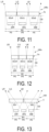
- FIG. 11 is a schematic view illustrating an electro-optical device 100 x including a color filter 5 x in the related art. “x” is added to the reference signs of elements associated with the electro-optical device 100 x in the related art.
- the color filter 5 x included in the electro-optical device 100 x includes a filter corresponding to the light-emitting element 20 x for each sub-pixel P 0 .
- the color filter 5 x includes a filter 50 x R that selectively transmits light in the red wavelength region, a filter 50 x G that selectively transmits light in the green wavelength region, and a filter 50 x B that selectively transmits light in the blue wavelength region.
- a plan view is omitted, the filter 50 x R overlaps the light-emitting element 20 R in plan view, the filter 50 x G overlaps the light-emitting element 20 G in plan view, and the filter 50 x B overlaps the light-emitting element 20 B in plan view.
- the electro-optical device 100 x light LG in the green wavelength region emitted from the light-emitting element 20 G is transmitted through the filter 50 x G.
- the light LG in the green wavelength region is absorbed by the filter 50 x R and the filter 50 x B adjacent to the filter 50 x G.
- light LR in the red wavelength region emitted from the light-emitting element 20 R is transmitted through the filter 50 x R.
- the light LR in the red wavelength region is abosobed by the filter 50 x G and the filter 50 x B adjacent to the filter 50 x R.
- light LB in the blue wavelength region emitted from the light-emitting element 20 B is transmitted through the filter 50 x B.
- the light LB in the blue wavelength region is absorbed by the filter 50 x G and the filter 50 x R adjacent to the filter 50 x B.
- FIG. 12 is a schematic view illustrating an example of a case in which the electro-optical device 100 x of FIG. 11 is reduced in size.
- a width W 1 of the pixel P when a width W 1 of the pixel P is reduced, a width of each sub-pixel P 0 is also reduced. Note that a distance DO between the color filter 5 x and each light-emitting element 20 x is unchanged.
- a width of each of the filters 50 x also decreases.
- a spread angle of light transmitted through the color filter 5 x decreases. Specifically, a spread angle of the light LG transmitted through the filter 50 x G, a spread angle of the light LR transmitted through the filter 50 x R, and a spread angle of the light LB transmitted through the filter 50 x B decrease.
- FIG. 13 is a schematic view illustrating the electro-optical device 100 of the first exemplary embodiment.
- the color filter 5 of this exemplary embodiment includes two types of filters, and the filters are not disposed for each sub-pixel P 0 . Therefore, in the electro-optical device 100 , the number of types of filters included in the color filter 5 is less than the number of types of the light-emitting elements 20 . Then, in the electro-optical device 100 , the yellow filter 50 Y overlaps the light-emitting element 20 R and the light-emitting element 20 G in plan view, and the cyan filter 50 C overlaps the light-emitting element 20 G and the light-emitting element 20 B in plan view.
- the light LG in the green wavelength region emitted from the light-emitting element 20 G is transmitted through the yellow filter 50 Y and the cyan filter 50 C.
- the light LG is transmitted through the color filter 5 without being absorbed by the color filter 5 .
- the number of types of filters included in the color filter 5 is less than the number of types of light-emitting elements 20 . Therefore, the width of each filter can be made larger than that in the related art. Thus, the width of the yellow filter 50 Y can be made large compared to the width of the filter 50 x R in the related art.
- the spread angle of the light LR transmitted through the yellow filter 50 Y can be made greater than the spread angle of the light LR transmitted through the filter 50 x R in the related art.
- the width of the cyan filter 50 C can be made large compared to the width of the filter 50 x B in the related art.
- the spread angle of the light LB transmitted through the cyan filter 50 C can be made greater than the spread angle of the light LB transmitted through the filter 50 x B in the related art.
- the light-emitting element layer 2 includes the light-emitting element 20 R that emits light in the red wavelength region, the light-emitting element 20 G that emits light in the green wavelength region, and the light-emitting element 20 B that emits light in the blue wavelength region.
- the color filter 5 includes the yellow filter 50 Y that transmits light in the red wavelength region and light in the green wavelength region and absorbs light in the blue wavelength region, and the cyan filter 50 C that transmits light in the green wavelength region and light in the blue wavelength region and absorbs light in the red wavelength region.
- a planar area of each of the filters can be made large compared to a case in which three types of filters corresponding to each of the three types of light-emitting elements 20 are provided.
- the spread angle of light is suppressed from becoming smaller than that in the related art. Therefore, even if the width of the sub-pixels P 0 decreases or the density of the sub-pixels P 0 increases, it is possible to suppress the possibility of deterioration in visual field angle characteristics. Further, the absorbing of the light from each of the light-emitting elements 20 by the filter is suppressed, and thus an opening ratio of each of the sub-pixels P 0 can be improved.
- the color filter 5 includes the two types of filters that transmit light in the green wavelength region.
- light in the green wavelength region is less likely to be absorbed by the filter compared to light in the wavelength regions of other colors.
- an intensity of light in the green wavelength region is higher than intensities of light in other wavelength regions in accordance with a desired color balance, a difference in the intensities of light in each wavelength region can be suppressed by using two types of filters that transmit light in the green wavelength region.
- a total area of the light-emitting region AG in each of the pixels P is largest.
- the light-emitting region AR overlaps the yellow filter 50 Y in plan view. Therefore, the light from the light-emitting region AR can be efficiently made incident on the yellow filter 50 Y compared to a case in which the yellow filter 50 Y is disposed offset with respect to the light-emitting region AR in plan view.
- the light-emitting region AB overlaps the cyan filter 50 C in plan view. Therefore, the light from the light-emitting region AB can be efficiently made incident on the cyan filter 50 C compared to a case in which the cyan filter 50 C is disposed offset with respect to the light-emitting region AB in plan view.
- the light-emitting region AG overlaps both the yellow filter 50 Y and the cyan filter 50 C in plan view. Therefore, the light from the light-emitting region AG can be efficiently made incident on the yellow filter 50 Y and the cyan filter 50 C compared to a case in which the yellow filter 50 Y and the cyan filter 50 C are disposed offset with respect to the light-emitting region AG in plan view. Accordingly, the electro-optical device 100 that is bright and has a wide visual field angle can be realized.
- the array of the light-emitting regions A is a Bayer array, and each of the light-emitting regions AG overlaps both the yellow filter 50 Y and the cyan filter 50 C in plan view. Therefore, in one pixel P, the yellow filter 50 Y and the cyan filter 50 C are disposed side by side in the ⁇ 2 direction intersecting the ⁇ 1 direction in which the two light-emitting regions AG are aligned. Put another way, the color filter 5 is disposed with respect to the light-emitting element layer 2 so that the array direction of the plurality of pixels P and the array direction of the plurality of yellow filters 50 Y and the plurality of cyan filters 50 C intersect.
- each of the pixels P two filters are disposed with respect to the four light-emitting regions A arranged in two rows and two columns.
- an increase in the total number of the yellow filters 50 Y and the cyan filters 50 C can be suppressed. Therefore, the yellow filters 50 Y and the cyan filters 50 C can be efficiently disposed.
- the yellow filter 50 Y located at the light-emitting region AR is disposed projecting from the light-emitting region AR to the four adjacent light-emitting regions AG in plan view.
- the cyan filter 50 C located at the light-emitting region AB is disposed projecting from the light-emitting region AB to the four adjacent light-emitting regions AG in plan view.
- a portion of the yellow filter 50 Y and a portion of the cyan filter 50 C overlap the light-emitting region AG in plan view.
- light in the red wavelength region from the light-emitting region AR spreads from the light-emitting region AR onto the four adjacent light-emitting regions AG and is transmitted through the yellow filter 50 Y.
- light in the blue wavelength region from the light-emitting region AB spreads from the light-emitting region AB onto the four adjacent light-emitting regions AG and is transmitted through the cyan filter 50 C.
- light in the green wavelength region from the light-emitting region AG is transmitted through the yellow filter 50 Y and the cyan filter 50 C. Therefore, light in the green wavelength region from the light-emitting region AG is transmitted through the color filter 5 without being absorbed by the filter.
- the electro-optical device 100 Accordingly, according to the electro-optical device 100 , light emitted from the light-emitting region A spreads in the X1, X2, Y1, and Y2 directions from the light-emitting region A and is transmitted through the color filter 5 . Therefore, even if the width of the sub-pixels P 0 decreases or the density of the sub-pixels P 0 increases, it is possible to effectively suppress deterioration in visual field angle characteristics.
- the array of the light-emitting elements 20 being a Bayer array
- the three types of light-emitting elements 20 are disposed in two rows and two columns in each of the pixels P. Therefore, for example, the visual field angle characteristics can be improved compared to a stripe array in which three types of light-emitting elements 20 are aligned in three row and one column, and a rectangle array described later.
- the difference in visual field angle characteristics in the X1, X2, Y1, and Y2 directions can be reduced due to the combination of the sub-pixels P 0 adjacent to one another.
- the light-emitting element layer 2 in which the array of the light-emitting elements 20 is a Bayer array and the color filter 5 it is possible to suppress deterioration in visual field angle characteristics in various directions.
- the light-emitting element 20 R, the light-emitting element 20 G, and the light-emitting element 20 B have mutually different optical resonance structures 29 .
- the light-emitting element 20 R has the optical resonance structure 29 R that intensifies light in the red wavelength region
- the light-emitting element 20 G has the optical resonance structure 29 G that intensifies light in the green wavelength region
- the light-emitting element 20 B has the optical resonance structure 29 B that intensifies light in the blue wavelength region.
- FIG. 14 is a schematic plan view illustrating a portion of a color filter 5 A in the second exemplary embodiment.
- the second exemplary embodiment is the same as the first exemplary embodiment except that the color filter 5 A is different from the color filter 5 of the first exemplary embodiment.
- items of the color filter 5 A different from those of the color filter 5 of the first exemplary embodiment will be described, and description of the same items will be omitted.
- the plurality of yellow filters 50 Y and the plurality of cyan filters 50 C included in the color filter 5 A illustrated in FIG. 14 are arranged alternately in a stripe pattern.
- the color filter 5 A two types of long filters of different colors are arranged alternately.
- the yellow filter 50 Y and the cyan filter 50 C each have a long shape in plan view extending in the Y2 direction.
- FIG. 15 is a schematic plan view illustrating an arrangement of the light-emitting element layer 2 and the color filter 5 A in the second exemplary embodiment.
- the plurality of yellow filters 50 Y and the plurality of cyan filters 50 C are arranged alternately in the X1 direction corresponding to the row direction of the plurality of light-emitting regions A.
- the yellow filters 50 Y are disposed in odd number columns of the light-emitting regions A
- the cyan filters 50 C are disposed in even number columns of the light-emitting regions A. Note that the column of the light-emitting regions A existing farthest in the X2 direction is a first column.
- each of the yellow filters 50 Y overlaps all of the light-emitting regions A existing in the corresponding column in plan view.
- each of the yellow filters 50 Y overlaps three light-emitting regions AR and three light-emitting regions AG alternately arranged in the Y2 direction in plan view.
- each of the cyan filters 50 C overlaps all of the light-emitting regions A existing in the corresponding column in plan view.
- each of the cyan filters 50 C overlaps three light-emitting regions AG and three light-emitting regions AB alternately arranged in the Y2 direction in plan view.
- respective widths of the yellow filter 50 Y and the cyan filter 50 C are slightly larger than a width of the light-emitting region A, but may be equal. Note that the width is a length in the X1 direction.
- each pixel P two types of filters, one yellow filter 50 Y and one cyan filter 50 C, are disposed in each pixel P.
- the light-emitting region AR overlaps the yellow filter 50 Y in plan view.
- the light-emitting region AB overlaps the cyan filter 50 C in plan view.
- the light-emitting region AG positioned in the Y2 direction with respect to the light-emitting region AR overlaps the yellow filter 50 Y in plan view.
- the light-emitting region AG positioned in the X1 direction with respect to the light-emitting region AR overlaps the cyan filter 50 C in plan view.
- the light-emitting region AG positioned in the Y2 direction with respect to the light-emitting region AR corresponds to the “second light-emitting element”
- the light-emitting region AG positioned in the X1 direction with respect to the light-emitting region AR corresponds to the “fourth light-emitting element”.
- deterioration in the visual field angle characteristics and a decrease in the opening ratio can be suppressed even if the width of the sub-pixels P 0 decreases or the density of the sub-pixels P 0 increases.
- the array of the light-emitting regions A is a Bayer array, one of the light-emitting regions AG overlaps the yellow filter 50 Y in plan view, and the other light-emitting region AG overlaps the cyan filter 50 C. Therefore, the yellow filter 50 Y and the cyan filter 50 C are disposed in a stripe pattern. Thus, the total number of the yellow filters 50 Y and the cyan filters 50 C can be further reduced, and the yellow filters 50 Y and the cyan filters 50 C can be more efficiently disposed, than in the first exemplary embodiment.
- each of the yellow filters 50 Y has a long shape extending in the Y2 direction and overlaps the plurality of light-emitting regions AR and the plurality of light-emitting regions AG aligned in the Y2 direction. Therefore, light in the red wavelength region from the light-emitting region AR spreads not only directly above the light-emitting region AR but also in the Y1 direction and the Y2 direction from the light-emitting region AR and is transmitted through the yellow filter 50 Y.
- each of the cyan filters 50 C has a long shape extending in the Y2 direction and overlaps the plurality of light-emitting regions AG and the plurality of light-emitting regions AB aligned in the Y2 direction. Therefore, light in the blue wavelength region from the light-emitting region AB spreads not only directly above the light-emitting region AB but also in the Y1 direction and the Y2 direction from the light-emitting region AB and is transmitted through the cyan filter 50 C. Furthermore, light in the green wavelength region from the light-emitting region AG is transmitted through the color filter 5 A without being absorbed by the filter.
- the electro-optical device 100 of this exemplary embodiment is effective for use in devices that particularly require visual field angle characteristics in the Y1 direction and the Y2 direction. It is desirable to select an optimum form in accordance with intended use.
- the light-emitting element layer 2 and the color filter 5 A of the second exemplary embodiment described above can also, similar to the first exemplary embodiment, improve visual field angle characteristics.
- a third exemplary embodiment will be described. Note that, for elements having the same functions as those of the first exemplary embodiment in each of the following examples, the reference signs used in the description of the first exemplary embodiment will be used and detailed description thereof will be omitted as appropriate.
- FIG. 16 is a schematic plan view illustrating a portion of a color filter 5 B in the third exemplary embodiment.
- the third exemplary embodiment is the same as the first exemplary embodiment except that the color filter 5 B is different from the color filter 5 of the first exemplary embodiment.
- items of the color filter 5 B that differ from those of the color filter 5 of the first exemplary embodiment will be described, and description of the same items will be omitted.
- the plurality of yellow filters 50 Y and the plurality of cyan filters 50 C included in the color filter 5 B illustrated in FIG. 16 are arranged alternately in a stripe pattern.
- the color filter 5 B two types of long filters of different colors are arranged alternately.
- the yellow filter 50 Y and the cyan filter 50 C each have a long shape in plan view extending in the X1 direction. Note that the direction in which the color filter 5 B of this exemplary embodiment is aligned is different from the direction in which the color filter 5 of the second exemplary embodiment is aligned.
- FIG. 17 is a schematic plan view illustrating an arrangement of the light-emitting element layer 2 and the color filter 5 B in the third exemplary embodiment.
- the plurality of yellow filters 50 Y and the plurality of cyan filters 50 C are arranged alternately in the Y2 direction corresponding to the column direction of the plurality of light-emitting regions A.
- the yellow filters 50 Y are disposed in odd number row of the light-emitting regions A
- the cyan filters 50 C are disposed in even number rows of the light-emitting regions A. Note that the row of the light-emitting regions A existing farthest in the Y1 direction is a first row.
- Each of the yellow filters 50 Y overlaps all of the light-emitting regions A existing in the corresponding row in plan view.
- each of the yellow filters 50 Y overlaps three light-emitting regions AR and three light-emitting regions AG alternately arranged in the X1 direction in plan view.
- each of the cyan filters 50 C overlaps all of the light-emitting regions A existing in the corresponding row in plan view.
- each of the cyan filters 50 C overlaps three light-emitting regions AG and three light-emitting regions AB alternately arranged in the X1 direction in plan view. Therefore, the yellow filter 50 Y and the cyan filter 50 C are disposed in a stripe pattern. Note that the width is a length in the Y1 direction.
- each pixel P two types of filters, one yellow filter 50 Y and one cyan filter 50 C, are disposed in each pixel P.
- the light-emitting region AR overlaps the yellow filter 50 Y in plan view.
- the light-emitting region AB overlaps the cyan filter 50 C in plan view.
- the light-emitting region AG positioned in the X1 direction with respect to the light-emitting region AR overlaps the yellow filter 50 Y in plan view.
- the light-emitting region AG positioned in the Y2 direction with respect to the light-emitting region AR overlaps the cyan filter 50 C in plan view.
- the light-emitting region AG positioned in the X1 direction with respect to the light-emitting region AR corresponds to the “second light-emitting element”
- the light-emitting region AG positioned in the Y2 direction with respect to the light-emitting region AR corresponds to the “fourth light-emitting element”.
- deterioration in the visual field angle characteristics and a decrease in the opening ratio can be suppressed even if the width of the sub-pixels P 0 decrease or the density of the sub-pixels P 0 increases.
- the array of the light-emitting regions A is a Bayer array, one of the light-emitting regions AG overlaps the yellow filter 50 Y in plan view, and the other light-emitting region AG overlaps the cyan filter 50 C. Therefore, the yellow filter 50 Y and the cyan filter 50 C are disposed in a stripe pattern. Thus, the total number of the yellow filters 50 Y and the cyan filters 50 C can be further reduced, and the yellow filters 50 Y and the cyan filters 50 C can be more efficiently disposed, than in the first exemplary embodiment.
- each of the yellow filters 50 Y has a long shape extending in the X1 direction and overlaps the plurality of light-emitting regions AR and the plurality of light-emitting regions AG aligned in the X1 direction. Therefore, light in the red wavelength region from the light-emitting region AR spreads not only directly above the light-emitting region AR but also in the X1 direction and the X2 direction from the light-emitting region AR and is transmitted through the yellow filter 50 Y. Further, in plan view, each of the cyan filters 50 C has a long shape extending in the X1 direction and overlaps the plurality of light-emitting regions AG and the plurality of light-emitting regions AB aligned in the X1 direction.
- light in the blue wavelength region from the light-emitting region AB spreads not only directly above the light-emitting region AB but also in the X1 direction and the X2 direction from the light-emitting region AB and is transmitted through the cyan filter 50 C. Furthermore, light in the green wavelength region from the light-emitting region AG is transmitted through the color filter 5 B without being absorbed by the filter.
- the electro-optical device 100 of this exemplary embodiment is effective for use in devices that particularly require visual field angle characteristics in the X1 direction and the X2 direction. It is desirable to select an optimum form in accordance with intended use.
- the light-emitting element layer 2 and the color filter 5 B of the third exemplary embodiment described above can also, similar to the first exemplary embodiment, improve the visual field angle characteristics.
- a fourth exemplary embodiment will be described. Note that, for elements having the same functions as those of the third exemplary embodiment in each of the following examples, the reference signs used in the description of the third exemplary embodiment will be used and detailed description thereof will be omitted as appropriate.
- FIG. 18 is a schematic plan view illustrating a portion of a light-emitting element layer 2 C of a fourth exemplary embodiment.
- the fourth exemplary embodiment is the same as the third exemplary embodiment except that the light-emitting element layer 2 C is different from the light-emitting element layer 2 of the first exemplary embodiment.
- items of the light-emitting element 2 C that differ from those of the light-emitting element 2 of the third exemplary embodiment will be described, and description of the same items will be omitted.
- the array of the sub-pixels P 0 is a rectangle array.
- the rectangle array is an array in which one sub-pixel PR, one sub-pixel PG, and one sub-pixel PB form a single pixel P, and differs from a stripe array.
- the direction in which the three sub-pixels P 0 in the rectangle array are aligned is not one direction.
- the light-emitting element layer 2 C includes one light-emitting element 20 R, one light-emitting element 20 G, and one light-emitting element 20 B for each pixel P.
- the array of the light-emitting regions A is a rectangle array.
- one light-emitting region AR, one light-emitting region AG, and one light-emitting region AB constitute one set.
- the direction in which the light-emitting region AR and the light-emitting region AB are aligned differs from the direction in which the light-emitting region AR and the light-emitting region AG are aligned and the direction in which the light-emitting region AB and the light-emitting region AG are aligned.
- the direction in which the light-emitting region AR and the light-emitting region AG are aligned and the direction in which the light-emitting region AB and the light-emitting region AG are aligned are the same, and in the illustrated example, the direction is the X1 direction.
- the direction in which the light-emitting region AR and the light-emitting region AB are aligned is the Y2 direction.
- the area of the light-emitting region AG of the three light-emitting regions A is largest.
- the light-emitting region AG is rectangular, and each of the light-emitting region AR and the light-emitting region AB is square.
- the light-emitting region AG is wider than the light-emitting regions AR and AB.
- the areas of the light-emitting regions AR and AB in plan view are equal to each other, but may be different from each other.
- the plurality of light-emitting regions AR and the plurality of light-emitting regions AB are aligned in the Y2 direction.
- the plurality of light-emitting regions AG are aligned in the Y2 direction.
- the columns in which the plurality of light-emitting regions AR and the plurality of light-emitting regions AB are aligned and the columns in which the plurality of light-emitting regions AG are aligned are alternately disposed in the X1 direction.
- one light-emitting region AR, one light-emitting region AG, and one light-emitting region AB of each pixel P in this exemplary embodiment are considered to fall within two rows and two columns of the sub-pixel P 0 of the first exemplary embodiment.
- the area of the light-emitting region AG in plan view of this exemplary embodiment is greater than or equal to a total area of the two light-emitting regions AG in plan view of the first exemplary embodiment.
- FIG. 19 is a schematic plan view illustrating an arrangement of the light-emitting element layer 2 C and the color filter 5 B in the fourth exemplary embodiment.
- the light-emitting region AR overlaps the yellow filter 50 Y in plan view.
- the light-emitting region AB overlaps the cyan filter 50 C in plan view.
- the light-emitting region AG includes a portion overlapping the yellow filter 50 Y and a portion overlapping the cyan filter 50 C.
- the light-emitting region AG overlaps both the yellow filter 50 Y and the cyan filter 50 C in plan view.
- light in the red wavelength region from the light-emitting region AR spreads from the light-emitting region AR in the X1 direction and the X2 direction and is transmitted through the yellow filter 50 Y.
- light in the blue wavelength region from the light-emitting region AB spreads from the light-emitting region AB in the X1 direction and the X2 direction and is transmitted through the cyan filter 50 C.
- light in the green wavelength region from the light-emitting region AG is transmitted through the color filter 5 B without being absorbed by the filter.
- the light-emitting element layer 2 C and the color filter 5 B it is possible to suppress the absorbing of light from the light-emitting elements 20 by the filter. This makes it possible to improve the opening ratio for each sub-pixel P 0 and improve the visual field angle characteristics.
- the array of the light-emitting regions AR, AG, AB is a rectangle array, and a planar area of the light-emitting region AG is largest. Then, the plurality of yellow filters 50 Y and the plurality of cyan filters 50 C are arranged in a stripe pattern in the direction in which the light-emitting region AR and the light-emitting region AB are aligned.
- the plurality of yellow filters 50 Y and the plurality of cyan filters 50 C are disposed in a stripe pattern, and thus a filter need not be provided for each of the three types of sub-pixels P 0 .
- each filter and the light-emitting element layer 2 C can be brought into close contact over a wider area compared to a case in which a filter is disposed for each of the three types of sub-pixels P 0 . This facilitates design and manufacture.
- the Bayer array of the first exemplary embodiment four of the light-emitting elements 20 are provided for each of the pixels P.
- the rectangle array three of the light-emitting elements 20 are provided for each of the pixels P.
- the light-emitting element layer 2 C and the color filter 5 B of the fourth exemplary embodiment described above can also, similar to the third exemplary embodiment, improve the visual field angle characteristics.
- the light-emitting element 20 has the optical resonance structure 29 having a different resonance wavelength for each color, the light-emitting element need not have the optical resonance structure 29 .
- the light-emitting element layer 2 may, for example, include a partition wall configured to partition the organic layer 24 for each of the light-emitting elements 20 .
- the light-emitting element 20 may include different light-emitting materials for each of the sub-pixels P 0 .
- the pixel electrode 23 may have light reflectivity. In this case, the reflection layer 21 may be omitted.
- the common electrode 25 is common to the plurality of light-emitting elements 20 , an individual cathode may be provided for each of the light-emitting elements 20 .
- the filters of the color filter 5 are disposed in contact with each other, but a so-called black matrix may be interposed between the filters of the color filter 5 . Further, the filters of the color filter 5 may include portions that overlap each other. Note that the same applies to other exemplary embodiments.
- the array of the light-emitting regions A is not limited to a Bayer array and a rectangle array, and may be, for example, a delta array or a stripe array.
- the “electro-optical device” is not limited to an organic EL device, and may be an inorganic EL device that uses an inorganic material or a p-light-emitting diode (LED) device.
- the row direction and the column direction of the plurality of pixels P may intersect at less than 90° rather than being orthogonal to each other.
- the row direction and the column direction of the plurality of filters in the first exemplary embodiment may intersect at less than 90° rather than being orthogonal to each other.
- the electro-optical device 100 of the exemplary embodiments described above is applicable to various electronic apparatuses.
- FIG. 20 is a plan view schematically illustrating a portion of a virtual display device 700 as an example of an electronic apparatus.
- the virtual display apparatus 700 illustrated in FIG. 20 is a head-mounted display (HMD) mounted on a head of an observer and configured to display an image.
- the virtual display apparatus 700 includes the electro-optical device 100 described above, a collimator 71 , a light guide 72 , a first reflection-type volume hologram 73 , a second reflection-type volume hologram 74 , and a control unit 79 . Note that light emitted from the electro-optical device 100 is emitted as image light LL.
- the control unit 79 includes a processor and a memory, for example, and controls the operation of the electro-optical device 100 .
- the collimator 71 is disposed between the electro-optical device 100 and the light guide 72 .
- the collimator 71 collimates light emitted from the electro-optical device 100 .
- the collimator 71 is constituted by a collimating lens or the like. The light collimated by the collimator 71 is incident on the light guide 72 .
- the light guide 72 has a flat plate shape, and is disposed so as to extend in a direction intersecting a direction of light incident via the collimator 71 .
- the light guide 72 reflects and guides light therein.
- a light incident port on which light is incident and a light emission port from which light is emitted are provided in a surface 721 of the light guide 72 facing the collimator 71 .
- the first reflection-type volume hologram 73 as a diffractive optical element and the second reflection-type volume hologram 74 as a diffractive optical element are disposed on a surface 722 of the light guide 72 opposite to the surface 721 .
- the second reflection-type volume hologram 74 is provided closer to the light emission port side than the first reflection-type volume hologram 73 .
- the first reflection-type volume hologram 73 and the second reflection-type volume hologram 74 have interference fringes corresponding to a predetermined wavelength region, and diffract and reflect light in the predetermined wavelength region.
- the image light LL incident on the light guide 72 from the light incident port travels while being repeatedly reflected, and is guided to an eye EY of an observer from a light emission port, and thus the observer can observe an image constituted by a virtual image formed by the image light LL.
- the virtual display apparatus 700 includes the electro-optical device 100 described above.
- the electro-optical device 100 described above has excellent visual field angle characteristics and good quality. Therefore, a virtual display apparatus 700 having high display quality can be provided by including the electro-optical device 100 .
- FIG. 21 is a perspective view illustrating a personal computer 400 as an example of the electronic apparatus in the present disclosure.
- the personal computer 400 illustrated in FIG. 21 includes the electro-optical device 100 , a main body 403 provided with a power switch 401 and a keyboard 402 , and a control unit 409 .
- the control unit 409 includes a processor and a memory, for example, and controls the operation of the electro-optical device 100 .
- the electro-optical device 100 has superior viewing angle characteristics and has good quality. Therefore, the personal computer 400 having high display quality can be provided by including the electro-optical device 100 .
- examples of the “electronic apparatus” including the electro-optical device 100 include, in addition to the virtual display apparatus 700 illustrated in FIG. 20 and the personal computer 400 illustrated in FIG. 21 , an apparatus disposed close to eyes such as a digital scope, a digital binocular, a digital still camera, and a video camera. Further, the “electronic apparatus” including the electro-optical device 100 is applied as a mobile phone, a smartphone, a personal digital assistant (PDA), a car navigation device, and a vehicle-mounted display unit. Furthermore, the “electronic apparatus” including the electro-optical device 100 is applied as illumination for illuminating light.
- PDA personal digital assistant
- the electro-optical device 100 is applied as illumination for illuminating light.
Landscapes
- Physics & Mathematics (AREA)
- Geometry (AREA)
- Engineering & Computer Science (AREA)
- Microelectronics & Electronic Packaging (AREA)
- Electroluminescent Light Sources (AREA)
- Devices For Indicating Variable Information By Combining Individual Elements (AREA)
- Optical Filters (AREA)
Abstract
Description
{(2×L0)/λ0+Φ}/(2π)=m0 (where m0 is an integer) [1]
Claims (6)
Applications Claiming Priority (2)
| Application Number | Priority Date | Filing Date | Title |
|---|---|---|---|
| JP2020-083828 | 2020-05-12 | ||
| JP2020083828A JP2021179492A (en) | 2020-05-12 | 2020-05-12 | Electro-optics and electronics |
Publications (2)
| Publication Number | Publication Date |
|---|---|
| US20210359016A1 US20210359016A1 (en) | 2021-11-18 |
| US12133440B2 true US12133440B2 (en) | 2024-10-29 |
Family
ID=78489102
Family Applications (1)
| Application Number | Title | Priority Date | Filing Date |
|---|---|---|---|
| US17/317,860 Active 2042-03-21 US12133440B2 (en) | 2020-05-12 | 2021-05-11 | Electro-optical device and electronic apparatus |
Country Status (3)
| Country | Link |
|---|---|
| US (1) | US12133440B2 (en) |
| JP (1) | JP2021179492A (en) |
| CN (1) | CN113658980B (en) |
Families Citing this family (1)
| Publication number | Priority date | Publication date | Assignee | Title |
|---|---|---|---|---|
| JP2021179495A (en) | 2020-05-12 | 2021-11-18 | セイコーエプソン株式会社 | Electro-optics and electronics |
Citations (23)
| Publication number | Priority date | Publication date | Assignee | Title |
|---|---|---|---|---|
| US20070200979A1 (en) | 2004-03-20 | 2007-08-30 | Rudin John C | Colour Display Device And Method Of Manufacture |
| US20100188322A1 (en) | 2009-01-26 | 2010-07-29 | Norimasa Furukawa | Color display unit |
| US20110095276A1 (en) | 2009-10-22 | 2011-04-28 | Sony Corporation | Display unit |
| US20140124802A1 (en) * | 2011-04-29 | 2014-05-08 | Kookmin University Industry Academy Cooperation Foundation | Full-color led display device and manufacturing method thereof |
| US9231034B1 (en) | 2014-01-07 | 2016-01-05 | Apple Inc. | Organic light-emitting diode displays |
| US20160025302A1 (en) * | 2014-07-25 | 2016-01-28 | Seiko Epson Corporation | Light-emitting device and electronic apparatus |
| JP2016136235A (en) | 2015-01-19 | 2016-07-28 | シャープ株式会社 | Display device and driving method thereof |
| JP2018084781A (en) | 2016-11-25 | 2018-05-31 | 大日本印刷株式会社 | Color filter, display device, and method of manufacturing color filter |
| US20180182814A1 (en) | 2016-12-22 | 2018-06-28 | Lg Display Co., Ltd. | Display device including color filters |
| US20180219050A1 (en) | 2017-02-01 | 2018-08-02 | Seiko Epson Corporation | Electrooptical device, electronic apparatus, and head mount display |
| JP2018125168A (en) | 2017-02-01 | 2018-08-09 | セイコーエプソン株式会社 | Electro-optic device and electronic equipment |
| JP2018124540A (en) | 2017-02-01 | 2018-08-09 | セイコーエプソン株式会社 | Electro-optical devices, electronic devices, head-mounted displays |
| US20180277610A1 (en) | 2017-03-24 | 2018-09-27 | Seiko Epson Corporation | Electrooptical device, manufacturing method of electrooptical device, and electronic equipment |
| US20190035862A1 (en) | 2017-07-31 | 2019-01-31 | Seiko Epson Corporation | Electro-optical device and electronic device |
| JP2019117941A (en) | 2019-03-19 | 2019-07-18 | セイコーエプソン株式会社 | Electro-optical device |
| US20190273122A1 (en) | 2018-03-01 | 2019-09-05 | Seiko Epson Corporation | Electro-optical device, manufacturing method of electro-optical device, and electronic apparatus |
| JP2019204763A (en) | 2017-11-30 | 2019-11-28 | 株式会社半導体エネルギー研究所 | Display panel, display device, display module, electronic device, and manufacturing method of display panel |
| US20200279517A1 (en) | 2019-01-30 | 2020-09-03 | Wuhan China Star Optoelectronics Semiconductor Display Technology Co., Ltd. | Organic light emitting diode display pixel array |
| US11020015B2 (en) * | 2015-10-09 | 2021-06-01 | Vasoptic Medical, Inc. | System and method for rapid examination of vasculature and particulate flow using laser speckle contrast imaging |
| US20210359015A1 (en) | 2020-05-12 | 2021-11-18 | Seiko Epson Corporation | Electro-optical device and electronic apparatus |
| US20210359013A1 (en) | 2020-05-12 | 2021-11-18 | Seiko Epson Corporation | Electro-optical device and electronic apparatus |
| US20210359017A1 (en) | 2020-05-12 | 2021-11-18 | Seiko Epson Corporation | Electro-optical device and electronic apparatus |
| US20220392879A1 (en) * | 2017-11-27 | 2022-12-08 | Seoul Viosys Co., Ltd. | Light emitting diode for display and display apparatus having the same |
Family Cites Families (10)
| Publication number | Priority date | Publication date | Assignee | Title |
|---|---|---|---|---|
| KR100190855B1 (en) * | 1995-12-22 | 1999-06-01 | 윤종용 | LCD color filter and manufacturing method thereof |
| US8023017B2 (en) * | 2007-01-08 | 2011-09-20 | United Microelectronics Corp. | Pattern of color filter array |
| JP2013012477A (en) * | 2011-06-28 | 2013-01-17 | Cbrite Inc | Hybrid full-color active matrix organic light emitting display |
| JP5950618B2 (en) * | 2012-02-24 | 2016-07-13 | キヤノン株式会社 | Method for forming light transmitting member and method for manufacturing imaging apparatus |
| JP5885608B2 (en) * | 2012-07-23 | 2016-03-15 | 株式会社東芝 | Solid-state imaging device |
| JP2015115345A (en) * | 2013-12-09 | 2015-06-22 | 株式会社東芝 | Solid-state imaging device |
| JP2015146304A (en) * | 2014-02-04 | 2015-08-13 | ソニー株式会社 | Display device and electronic device |
| JP6318676B2 (en) * | 2014-02-14 | 2018-05-09 | セイコーエプソン株式会社 | Organic light emitting device manufacturing method, organic light emitting device, and electronic apparatus |
| CN106531896B (en) * | 2016-12-13 | 2018-08-10 | 上海天马有机发光显示技术有限公司 | Organic light emitting display device, manufacturing method thereof, and organic light emitting display device |
| JP6930565B2 (en) * | 2017-06-30 | 2021-09-01 | セイコーエプソン株式会社 | Electro-optics |
-
2020
- 2020-05-12 JP JP2020083828A patent/JP2021179492A/en active Pending
-
2021
- 2021-05-10 CN CN202110504368.1A patent/CN113658980B/en active Active
- 2021-05-11 US US17/317,860 patent/US12133440B2/en active Active
Patent Citations (29)
| Publication number | Priority date | Publication date | Assignee | Title |
|---|---|---|---|---|
| US20070200979A1 (en) | 2004-03-20 | 2007-08-30 | Rudin John C | Colour Display Device And Method Of Manufacture |
| US20100188322A1 (en) | 2009-01-26 | 2010-07-29 | Norimasa Furukawa | Color display unit |
| US20110095276A1 (en) | 2009-10-22 | 2011-04-28 | Sony Corporation | Display unit |
| JP2011090894A (en) | 2009-10-22 | 2011-05-06 | Sony Corp | Display device |
| US20140124802A1 (en) * | 2011-04-29 | 2014-05-08 | Kookmin University Industry Academy Cooperation Foundation | Full-color led display device and manufacturing method thereof |
| US9231034B1 (en) | 2014-01-07 | 2016-01-05 | Apple Inc. | Organic light-emitting diode displays |
| US20160025302A1 (en) * | 2014-07-25 | 2016-01-28 | Seiko Epson Corporation | Light-emitting device and electronic apparatus |
| JP2016136235A (en) | 2015-01-19 | 2016-07-28 | シャープ株式会社 | Display device and driving method thereof |
| US11020015B2 (en) * | 2015-10-09 | 2021-06-01 | Vasoptic Medical, Inc. | System and method for rapid examination of vasculature and particulate flow using laser speckle contrast imaging |
| JP2018084781A (en) | 2016-11-25 | 2018-05-31 | 大日本印刷株式会社 | Color filter, display device, and method of manufacturing color filter |
| US20180182814A1 (en) | 2016-12-22 | 2018-06-28 | Lg Display Co., Ltd. | Display device including color filters |
| US20180219050A1 (en) | 2017-02-01 | 2018-08-02 | Seiko Epson Corporation | Electrooptical device, electronic apparatus, and head mount display |
| JP2018125168A (en) | 2017-02-01 | 2018-08-09 | セイコーエプソン株式会社 | Electro-optic device and electronic equipment |
| JP2018124540A (en) | 2017-02-01 | 2018-08-09 | セイコーエプソン株式会社 | Electro-optical devices, electronic devices, head-mounted displays |
| JP2018163734A (en) | 2017-03-24 | 2018-10-18 | セイコーエプソン株式会社 | Electro-optical device, method of manufacturing electro-optical device, and electronic apparatus |
| US20180277610A1 (en) | 2017-03-24 | 2018-09-27 | Seiko Epson Corporation | Electrooptical device, manufacturing method of electrooptical device, and electronic equipment |
| US20190035862A1 (en) | 2017-07-31 | 2019-01-31 | Seiko Epson Corporation | Electro-optical device and electronic device |
| US20220392879A1 (en) * | 2017-11-27 | 2022-12-08 | Seoul Viosys Co., Ltd. | Light emitting diode for display and display apparatus having the same |
| US20230269987A1 (en) | 2017-11-30 | 2023-08-24 | Semiconductor Energy Laboratory Co., Ltd. | Display Panel, Display Device, Display Module, Electronic Device, and Manufacturing Method of Display Panel |
| JP2019204763A (en) | 2017-11-30 | 2019-11-28 | 株式会社半導体エネルギー研究所 | Display panel, display device, display module, electronic device, and manufacturing method of display panel |
| US20200357863A1 (en) | 2017-11-30 | 2020-11-12 | Semiconductor Energy Laboratory Co., Ltd. | Display Panel, Display Device, Display Module, Electronic Device, and Manufacturing Method of Display Panel |
| US20200295091A1 (en) | 2018-03-01 | 2020-09-17 | Seiko Epson Corporation | Electro-optical device, manufacturing method of electro-optical device, and electronic apparatus |
| JP2019153411A (en) | 2018-03-01 | 2019-09-12 | セイコーエプソン株式会社 | Electro-optical device, method of manufacturing the same, and electronic apparatus |
| US20190273122A1 (en) | 2018-03-01 | 2019-09-05 | Seiko Epson Corporation | Electro-optical device, manufacturing method of electro-optical device, and electronic apparatus |
| US20200279517A1 (en) | 2019-01-30 | 2020-09-03 | Wuhan China Star Optoelectronics Semiconductor Display Technology Co., Ltd. | Organic light emitting diode display pixel array |
| JP2019117941A (en) | 2019-03-19 | 2019-07-18 | セイコーエプソン株式会社 | Electro-optical device |
| US20210359015A1 (en) | 2020-05-12 | 2021-11-18 | Seiko Epson Corporation | Electro-optical device and electronic apparatus |
| US20210359013A1 (en) | 2020-05-12 | 2021-11-18 | Seiko Epson Corporation | Electro-optical device and electronic apparatus |
| US20210359017A1 (en) | 2020-05-12 | 2021-11-18 | Seiko Epson Corporation | Electro-optical device and electronic apparatus |
Non-Patent Citations (1)
| Title |
|---|
| Mantidtings, "Concerned about the pixel arrangement on the 8K or the 8KX? Here's some insight from the professionals on the issue," available at: https://community.openmr.com/t/concerned-about-the-pixel-arrangement-on-the-8k-or-the-8kx-heres-some-insight-from-the-professionals-on-the-issue/8690. |
Also Published As
| Publication number | Publication date |
|---|---|
| US20210359016A1 (en) | 2021-11-18 |
| CN113658980A (en) | 2021-11-16 |
| CN113658980B (en) | 2023-07-18 |
| JP2021179492A (en) | 2021-11-18 |
Similar Documents
| Publication | Publication Date | Title |
|---|---|---|
| US12376472B2 (en) | Display device having lens corresponding to pixel, and electronic apparatus | |
| US11552274B2 (en) | Display device having pixel electrode and color filter, and electronic apparatus | |
| US20220158135A1 (en) | Electro-optical device and electronic apparatus | |
| US11539034B2 (en) | Display device and electronic apparatus having lenses disposed correspondingly to respective pixel electrodes | |
| US20170236880A1 (en) | Electro-optical device and electronic apparatus | |
| US12245486B2 (en) | Electro-optical device and electronic apparatus | |
| US20250031517A1 (en) | Display device and electronic apparatus | |
| US20200358033A1 (en) | Organic el display device and electronic apparatus | |
| US20210359015A1 (en) | Electro-optical device and electronic apparatus | |
| CN113671765B (en) | Electro-optic devices and electronics | |
| US20210359013A1 (en) | Electro-optical device and electronic apparatus | |
| US12075679B2 (en) | Electro-optical device and electronic apparatus | |
| US12133440B2 (en) | Electro-optical device and electronic apparatus | |
| CN113658983B (en) | Electro-optic devices and electronics | |
| US11641771B2 (en) | Electro-optical device and electronic apparatus | |
| US12317676B2 (en) | Electro-optical device and electronic apparatus | |
| KR20250033489A (en) | Display Apparatus | |
| JP2024033966A (en) | Display devices and electronic equipment |
Legal Events
| Date | Code | Title | Description |
|---|---|---|---|
| FEPP | Fee payment procedure |
Free format text: ENTITY STATUS SET TO UNDISCOUNTED (ORIGINAL EVENT CODE: BIG.); ENTITY STATUS OF PATENT OWNER: LARGE ENTITY |
|
| AS | Assignment |
Owner name: SEIKO EPSON CORPORATION, JAPAN Free format text: ASSIGNMENT OF ASSIGNORS INTEREST;ASSIGNORS:KOSHIHARA, TAKESHI;IROBE, JUN;SIGNING DATES FROM 20210225 TO 20210303;REEL/FRAME:056254/0265 |
|
| STPP | Information on status: patent application and granting procedure in general |
Free format text: DOCKETED NEW CASE - READY FOR EXAMINATION |
|
| STPP | Information on status: patent application and granting procedure in general |
Free format text: NON FINAL ACTION MAILED |
|
| STPP | Information on status: patent application and granting procedure in general |
Free format text: RESPONSE TO NON-FINAL OFFICE ACTION ENTERED AND FORWARDED TO EXAMINER |
|
| STPP | Information on status: patent application and granting procedure in general |
Free format text: NOTICE OF ALLOWANCE MAILED -- APPLICATION RECEIVED IN OFFICE OF PUBLICATIONS |
|
| ZAAA | Notice of allowance and fees due |
Free format text: ORIGINAL CODE: NOA |
|
| ZAAB | Notice of allowance mailed |
Free format text: ORIGINAL CODE: MN/=. |
|
| STPP | Information on status: patent application and granting procedure in general |
Free format text: PUBLICATIONS -- ISSUE FEE PAYMENT VERIFIED |
|
| STCF | Information on status: patent grant |
Free format text: PATENTED CASE |
|
| STPP | Information on status: patent application and granting procedure in general |
Free format text: WITHDRAW FROM ISSUE AWAITING ACTION |
|
| STPP | Information on status: patent application and granting procedure in general |
Free format text: DOCKETED NEW CASE - READY FOR EXAMINATION |
|
| STPP | Information on status: patent application and granting procedure in general |
Free format text: NOTICE OF ALLOWANCE MAILED -- APPLICATION RECEIVED IN OFFICE OF PUBLICATIONS |
|
| ZAAB | Notice of allowance mailed |
Free format text: ORIGINAL CODE: MN/=. |
|
| STPP | Information on status: patent application and granting procedure in general |
Free format text: PUBLICATIONS -- ISSUE FEE PAYMENT VERIFIED |
|
| STCF | Information on status: patent grant |
Free format text: PATENTED CASE |