US20110095276A1 - Display unit - Google Patents
Display unit Download PDFInfo
- Publication number
- US20110095276A1 US20110095276A1 US12/899,133 US89913310A US2011095276A1 US 20110095276 A1 US20110095276 A1 US 20110095276A1 US 89913310 A US89913310 A US 89913310A US 2011095276 A1 US2011095276 A1 US 2011095276A1
- Authority
- US
- United States
- Prior art keywords
- light emitting
- layer
- emitting device
- organic light
- light
- Prior art date
- Legal status (The legal status is an assumption and is not a legal conclusion. Google has not performed a legal analysis and makes no representation as to the accuracy of the status listed.)
- Granted
Links
- 239000000463 material Substances 0.000 claims description 52
- 238000002347 injection Methods 0.000 claims description 50
- 239000007924 injection Substances 0.000 claims description 50
- IBHBKWKFFTZAHE-UHFFFAOYSA-N n-[4-[4-(n-naphthalen-1-ylanilino)phenyl]phenyl]-n-phenylnaphthalen-1-amine Chemical compound C1=CC=CC=C1N(C=1C2=CC=CC=C2C=CC=1)C1=CC=C(C=2C=CC(=CC=2)N(C=2C=CC=CC=2)C=2C3=CC=CC=C3C=CC=2)C=C1 IBHBKWKFFTZAHE-UHFFFAOYSA-N 0.000 claims description 34
- 230000005525 hole transport Effects 0.000 claims description 24
- 239000000126 substance Substances 0.000 claims description 23
- 239000000758 substrate Substances 0.000 claims description 20
- 238000009826 distribution Methods 0.000 claims description 14
- TVIVIEFSHFOWTE-UHFFFAOYSA-K tri(quinolin-8-yloxy)alumane Chemical compound [Al+3].C1=CN=C2C([O-])=CC=CC2=C1.C1=CN=C2C([O-])=CC=CC2=C1.C1=CN=C2C([O-])=CC=CC2=C1 TVIVIEFSHFOWTE-UHFFFAOYSA-K 0.000 claims description 12
- XSUNFLLNZQIJJG-UHFFFAOYSA-N 2-n-naphthalen-2-yl-1-n,1-n,2-n-triphenylbenzene-1,2-diamine Chemical compound C1=CC=CC=C1N(C=1C(=CC=CC=1)N(C=1C=CC=CC=1)C=1C=C2C=CC=CC2=CC=1)C1=CC=CC=C1 XSUNFLLNZQIJJG-UHFFFAOYSA-N 0.000 claims description 4
- -1 8-quinolinol aluminum Chemical compound 0.000 claims description 4
- 239000007983 Tris buffer Substances 0.000 claims description 4
- HFACYLZERDEVSX-UHFFFAOYSA-N benzidine Chemical compound C1=CC(N)=CC=C1C1=CC=C(N)C=C1 HFACYLZERDEVSX-UHFFFAOYSA-N 0.000 claims description 4
- 238000000926 separation method Methods 0.000 abstract description 13
- 230000002349 favourable effect Effects 0.000 abstract description 2
- 239000010410 layer Substances 0.000 description 333
- 239000012044 organic layer Substances 0.000 description 62
- 239000010408 film Substances 0.000 description 19
- 230000003247 decreasing effect Effects 0.000 description 14
- 239000000203 mixture Substances 0.000 description 13
- 238000001704 evaporation Methods 0.000 description 9
- 239000011241 protective layer Substances 0.000 description 8
- 238000007789 sealing Methods 0.000 description 8
- 230000015572 biosynthetic process Effects 0.000 description 7
- 238000005401 electroluminescence Methods 0.000 description 7
- 239000002585 base Substances 0.000 description 6
- OSQXTXTYKAEHQV-WXUKJITCSA-N 4-methyl-n-[4-[(e)-2-[4-[4-[(e)-2-[4-(4-methyl-n-(4-methylphenyl)anilino)phenyl]ethenyl]phenyl]phenyl]ethenyl]phenyl]-n-(4-methylphenyl)aniline Chemical compound C1=CC(C)=CC=C1N(C=1C=CC(\C=C\C=2C=CC(=CC=2)C=2C=CC(\C=C\C=3C=CC(=CC=3)N(C=3C=CC(C)=CC=3)C=3C=CC(C)=CC=3)=CC=2)=CC=1)C1=CC=C(C)C=C1 OSQXTXTYKAEHQV-WXUKJITCSA-N 0.000 description 5
- VBVAVBCYMYWNOU-UHFFFAOYSA-N coumarin 6 Chemical compound C1=CC=C2SC(C3=CC4=CC=C(C=C4OC3=O)N(CC)CC)=NC2=C1 VBVAVBCYMYWNOU-UHFFFAOYSA-N 0.000 description 5
- 239000011159 matrix material Substances 0.000 description 5
- 238000005215 recombination Methods 0.000 description 5
- 230000006798 recombination Effects 0.000 description 5
- 229910052782 aluminium Inorganic materials 0.000 description 4
- XAGFODPZIPBFFR-UHFFFAOYSA-N aluminium Chemical compound [Al] XAGFODPZIPBFFR-UHFFFAOYSA-N 0.000 description 4
- MWPLVEDNUUSJAV-UHFFFAOYSA-N anthracene Chemical compound C1=CC=CC2=CC3=CC=CC=C3C=C21 MWPLVEDNUUSJAV-UHFFFAOYSA-N 0.000 description 4
- 238000010586 diagram Methods 0.000 description 4
- 238000004770 highest occupied molecular orbital Methods 0.000 description 4
- 238000012986 modification Methods 0.000 description 4
- 230000004048 modification Effects 0.000 description 4
- PXHVJJICTQNCMI-UHFFFAOYSA-N Nickel Chemical compound [Ni] PXHVJJICTQNCMI-UHFFFAOYSA-N 0.000 description 3
- 229910045601 alloy Inorganic materials 0.000 description 3
- 239000000956 alloy Substances 0.000 description 3
- 238000004519 manufacturing process Methods 0.000 description 3
- 238000000034 method Methods 0.000 description 3
- BASFCYQUMIYNBI-UHFFFAOYSA-N platinum Chemical compound [Pt] BASFCYQUMIYNBI-UHFFFAOYSA-N 0.000 description 3
- 238000001228 spectrum Methods 0.000 description 3
- WHXSMMKQMYFTQS-UHFFFAOYSA-N Lithium Chemical compound [Li] WHXSMMKQMYFTQS-UHFFFAOYSA-N 0.000 description 2
- 229910052581 Si3N4 Inorganic materials 0.000 description 2
- BQCADISMDOOEFD-UHFFFAOYSA-N Silver Chemical compound [Ag] BQCADISMDOOEFD-UHFFFAOYSA-N 0.000 description 2
- 239000000872 buffer Substances 0.000 description 2
- 239000011575 calcium Substances 0.000 description 2
- 239000011651 chromium Substances 0.000 description 2
- 239000010949 copper Substances 0.000 description 2
- 230000000694 effects Effects 0.000 description 2
- 230000005684 electric field Effects 0.000 description 2
- 239000011521 glass Substances 0.000 description 2
- 239000010931 gold Substances 0.000 description 2
- 239000011810 insulating material Substances 0.000 description 2
- 238000009413 insulation Methods 0.000 description 2
- 239000004973 liquid crystal related substance Substances 0.000 description 2
- 229910052744 lithium Inorganic materials 0.000 description 2
- 239000011777 magnesium Substances 0.000 description 2
- 229910052751 metal Inorganic materials 0.000 description 2
- 239000002184 metal Substances 0.000 description 2
- 229910001092 metal group alloy Inorganic materials 0.000 description 2
- 239000011368 organic material Substances 0.000 description 2
- HQVNEWCFYHHQES-UHFFFAOYSA-N silicon nitride Chemical compound N12[Si]34N5[Si]62N3[Si]51N64 HQVNEWCFYHHQES-UHFFFAOYSA-N 0.000 description 2
- 239000004332 silver Substances 0.000 description 2
- 239000011734 sodium Substances 0.000 description 2
- 239000010936 titanium Substances 0.000 description 2
- DMEVMYSQZPJFOK-UHFFFAOYSA-N 3,4,5,6,9,10-hexazatetracyclo[12.4.0.02,7.08,13]octadeca-1(18),2(7),3,5,8(13),9,11,14,16-nonaene Chemical group N1=NN=C2C3=CC=CC=C3C3=CC=NN=C3C2=N1 DMEVMYSQZPJFOK-UHFFFAOYSA-N 0.000 description 1
- 229910001316 Ag alloy Inorganic materials 0.000 description 1
- 229910017073 AlLi Inorganic materials 0.000 description 1
- OYPRJOBELJOOCE-UHFFFAOYSA-N Calcium Chemical compound [Ca] OYPRJOBELJOOCE-UHFFFAOYSA-N 0.000 description 1
- VYZAMTAEIAYCRO-UHFFFAOYSA-N Chromium Chemical compound [Cr] VYZAMTAEIAYCRO-UHFFFAOYSA-N 0.000 description 1
- RYGMFSIKBFXOCR-UHFFFAOYSA-N Copper Chemical compound [Cu] RYGMFSIKBFXOCR-UHFFFAOYSA-N 0.000 description 1
- DGAQECJNVWCQMB-PUAWFVPOSA-M Ilexoside XXIX Chemical compound C[C@@H]1CC[C@@]2(CC[C@@]3(C(=CC[C@H]4[C@]3(CC[C@@H]5[C@@]4(CC[C@@H](C5(C)C)OS(=O)(=O)[O-])C)C)[C@@H]2[C@]1(C)O)C)C(=O)O[C@H]6[C@@H]([C@H]([C@@H]([C@H](O6)CO)O)O)O.[Na+] DGAQECJNVWCQMB-PUAWFVPOSA-M 0.000 description 1
- XEEYBQQBJWHFJM-UHFFFAOYSA-N Iron Chemical compound [Fe] XEEYBQQBJWHFJM-UHFFFAOYSA-N 0.000 description 1
- FUJCRWPEOMXPAD-UHFFFAOYSA-N Li2O Inorganic materials [Li+].[Li+].[O-2] FUJCRWPEOMXPAD-UHFFFAOYSA-N 0.000 description 1
- FYYHWMGAXLPEAU-UHFFFAOYSA-N Magnesium Chemical compound [Mg] FYYHWMGAXLPEAU-UHFFFAOYSA-N 0.000 description 1
- 229910000861 Mg alloy Inorganic materials 0.000 description 1
- ZOKXTWBITQBERF-UHFFFAOYSA-N Molybdenum Chemical compound [Mo] ZOKXTWBITQBERF-UHFFFAOYSA-N 0.000 description 1
- 229910052779 Neodymium Inorganic materials 0.000 description 1
- 239000004642 Polyimide Substances 0.000 description 1
- 229910004205 SiNX Inorganic materials 0.000 description 1
- VYPSYNLAJGMNEJ-UHFFFAOYSA-N Silicium dioxide Chemical compound O=[Si]=O VYPSYNLAJGMNEJ-UHFFFAOYSA-N 0.000 description 1
- XUIMIQQOPSSXEZ-UHFFFAOYSA-N Silicon Chemical compound [Si] XUIMIQQOPSSXEZ-UHFFFAOYSA-N 0.000 description 1
- RTAQQCXQSZGOHL-UHFFFAOYSA-N Titanium Chemical compound [Ti] RTAQQCXQSZGOHL-UHFFFAOYSA-N 0.000 description 1
- 239000012790 adhesive layer Substances 0.000 description 1
- 239000003513 alkali Substances 0.000 description 1
- 229910052784 alkaline earth metal Inorganic materials 0.000 description 1
- 230000002238 attenuated effect Effects 0.000 description 1
- 229910052791 calcium Inorganic materials 0.000 description 1
- 239000003990 capacitor Substances 0.000 description 1
- 230000008859 change Effects 0.000 description 1
- 229910052804 chromium Inorganic materials 0.000 description 1
- 239000011248 coating agent Substances 0.000 description 1
- 238000000576 coating method Methods 0.000 description 1
- 229910017052 cobalt Inorganic materials 0.000 description 1
- 239000010941 cobalt Substances 0.000 description 1
- GUTLYIVDDKVIGB-UHFFFAOYSA-N cobalt atom Chemical compound [Co] GUTLYIVDDKVIGB-UHFFFAOYSA-N 0.000 description 1
- 239000003086 colorant Substances 0.000 description 1
- 229910052802 copper Inorganic materials 0.000 description 1
- XUCJHNOBJLKZNU-UHFFFAOYSA-M dilithium;hydroxide Chemical compound [Li+].[Li+].[OH-] XUCJHNOBJLKZNU-UHFFFAOYSA-M 0.000 description 1
- 230000003467 diminishing effect Effects 0.000 description 1
- 238000011156 evaluation Methods 0.000 description 1
- PCHJSUWPFVWCPO-UHFFFAOYSA-N gold Chemical compound [Au] PCHJSUWPFVWCPO-UHFFFAOYSA-N 0.000 description 1
- 229910052737 gold Inorganic materials 0.000 description 1
- 229910052749 magnesium Inorganic materials 0.000 description 1
- 229910052750 molybdenum Inorganic materials 0.000 description 1
- 239000011733 molybdenum Substances 0.000 description 1
- YPJRZWDWVBNDIW-MBALSZOMSA-N n,n-diphenyl-4-[(e)-2-[4-[4-[(e)-2-[4-(n-phenylanilino)phenyl]ethenyl]phenyl]phenyl]ethenyl]aniline Chemical group C=1C=C(N(C=2C=CC=CC=2)C=2C=CC=CC=2)C=CC=1/C=C/C(C=C1)=CC=C1C(C=C1)=CC=C1\C=C\C(C=C1)=CC=C1N(C=1C=CC=CC=1)C1=CC=CC=C1 YPJRZWDWVBNDIW-MBALSZOMSA-N 0.000 description 1
- QEFYFXOXNSNQGX-UHFFFAOYSA-N neodymium atom Chemical compound [Nd] QEFYFXOXNSNQGX-UHFFFAOYSA-N 0.000 description 1
- 229910052759 nickel Inorganic materials 0.000 description 1
- AHLBNYSZXLDEJQ-FWEHEUNISA-N orlistat Chemical compound CCCCCCCCCCC[C@H](OC(=O)[C@H](CC(C)C)NC=O)C[C@@H]1OC(=O)[C@H]1CCCCCC AHLBNYSZXLDEJQ-FWEHEUNISA-N 0.000 description 1
- 238000000059 patterning Methods 0.000 description 1
- 229910052697 platinum Inorganic materials 0.000 description 1
- 229920001721 polyimide Polymers 0.000 description 1
- 230000001681 protective effect Effects 0.000 description 1
- 239000011347 resin Substances 0.000 description 1
- 229920005989 resin Polymers 0.000 description 1
- 230000004044 response Effects 0.000 description 1
- 230000000717 retained effect Effects 0.000 description 1
- 229910052710 silicon Inorganic materials 0.000 description 1
- 239000010703 silicon Substances 0.000 description 1
- 229910052814 silicon oxide Inorganic materials 0.000 description 1
- 229910052709 silver Inorganic materials 0.000 description 1
- 229910052708 sodium Inorganic materials 0.000 description 1
- 238000004544 sputter deposition Methods 0.000 description 1
- 229910052715 tantalum Inorganic materials 0.000 description 1
- GUVRBAGPIYLISA-UHFFFAOYSA-N tantalum atom Chemical compound [Ta] GUVRBAGPIYLISA-UHFFFAOYSA-N 0.000 description 1
- 239000010409 thin film Substances 0.000 description 1
- 229910052719 titanium Inorganic materials 0.000 description 1
- 239000012780 transparent material Substances 0.000 description 1
- WFKWXMTUELFFGS-UHFFFAOYSA-N tungsten Chemical compound [W] WFKWXMTUELFFGS-UHFFFAOYSA-N 0.000 description 1
- 229910052721 tungsten Inorganic materials 0.000 description 1
- 239000010937 tungsten Substances 0.000 description 1
Images


Classifications
-
- H—ELECTRICITY
- H10—SEMICONDUCTOR DEVICES; ELECTRIC SOLID-STATE DEVICES NOT OTHERWISE PROVIDED FOR
- H10K—ORGANIC ELECTRIC SOLID-STATE DEVICES
- H10K59/00—Integrated devices, or assemblies of multiple devices, comprising at least one organic light-emitting element covered by group H10K50/00
- H10K59/30—Devices specially adapted for multicolour light emission
- H10K59/38—Devices specially adapted for multicolour light emission comprising colour filters or colour changing media [CCM]
Definitions
- the present application relates to a display unit that includes a self-light emitting type organic light emitting device.
- an organic EL (Electro Luminescence) display unit using a self-light emitting type organic EL device including an organic layer has been practically used. Since the organic EL display unit is a self-light emitting type display unit, its view angle is wider than that of the liquid crystal display unit or the like. Further, the organic EL display unit has sufficient response to a high-definition and high-speed video signal.
- an organic EL display that has a combination structure of an organic light emitting device that emits white light (hereinafter referred to as a white light emitting device) and a color filter has been known.
- a full color display unit is able to be comparatively easily fabricated without separately forming each organic light emitting device that emits each color, that is, without performing fine separate coating operation using a metal mask in forming a light emitting layer.
- the white light emitting device has a structure in which, for example, two light emitting layers are layered in one light emitting unit sandwiched between an anode and a cathode, the two light emitting layers simultaneously emit light, and therefore white light emission is extracted as a whole.
- the white light emitting device examples include a so-called tandem type light emitting device in which a plurality of light emitting units are layered between a cathode and an anode with a charge generation layer in between (for example, refer to Japanese Unexamined Patent Application Publication No. 2006-324016).
- the tandem type light emitting device the plurality of light emitting units respectively having one or more light emitting layers are included. Whole light emitting color becomes white by overlapping respective light emitting colors from the respective light emitting units each other.
- a display unit including a multilayer structure in which a light emitting device group that respectively has a plurality of cyan organic light emitting devices emitting cyan light and a plurality of magenta organic light emitting devices emitting magenta light and a color filter group that has a plurality of blue filters transmitting blue light and a plurality of yellow filters transmitting yellow light are sequentially layered over a substrate.
- the cyan light and the magenta light are emitted from the light emitting device group, and the cyan light and the magenta light entering the color filter group is both converted to the blue light by the blue filter and is respectively converted to green light and red light by the yellow filter. Therefore, compared to a case that the light emitting device group emits white light, color separation is favorably performed even if the thickness of the color filter group is decreased.
- a display unit including a multilayer structure in which a light emitting device group that respectively has a plurality of cyan organic light emitting devices emitting cyan light and a plurality of magenta organic light emitting devices emitting magenta light and a color filter group that has a plurality of red filters transmitting red light, a plurality of green filters transmitting green light, and a plurality of blue filters transmitting blue light are sequentially layered over a substrate.
- the cyan light and the magenta light is emitted from the light emitting device group, and the cyan light and the magenta light enters the color filter group.
- the cyan light is converted to the blue light by the blue filter, or is converted to the green light by the green filter.
- the magenta light is converted to the blue light by the blue filter, or is converted to the red light by the red filter. Therefore, compared to a case that the light emitting device group emits white light, color separation is favorably performed even if the thickness of the color filter group is decreased.
- a display unit including a multilayer structure in which a light emitting device group that has at least two of a plurality of cyan organic light emitting devices emitting cyan light, a plurality of magenta organic light emitting devices emitting magenta light, and a plurality of yellow organic light emitting devices emitting yellow light and a color filter group that has a plurality of red filters transmitting red light, a plurality of green filters transmitting green light, and a plurality of blue filters transmitting blue light are sequentially layered over a substrate.
- the cyan light is converted to the blue light by the blue filter, or is converted to the green light by the green filter.
- the magenta light is converted to the blue light by the blue filter, or is converted to the red light by the red filter.
- the yellow light is converted to the green light by the green filter, or is converted to the red light by the red filter. Therefore, compared to a case that the light emitting device group emits white light, color separation is favorably performed even if the thickness of the color filter group is decreased.
- the light emitting device group has a plurality of organic light emitting devices that respectively emit the cyan light, the magenta light, or the yellow light.
- the thickness of the color filter group is able to be decreased while the color purity is maintained. In the result, the whole light emitting efficiency is improved, and the thickness of the whole structure is able to be decreased.
- FIG. 1 is a view illustrating a structure of a display unit according to a first embodiment.
- FIG. 2 is a view illustrating an example of the pixel drive circuit illustrated in FIG. 1 .
- FIG. 3 is a cross sectional view illustrating a schematic structure of the display device in the display region illustrated in FIG. 1 .
- FIG. 4 is a characteristics diagram illustrating an intensity distribution of cyan light.
- FIG. 5 is a characteristics diagram illustrating an intensity distribution of magenta light.
- FIG. 6 is an enlarged cross sectional view illustrating a structure of the organic light emitting device illustrated in FIG. 3 .
- FIG. 7 is a characteristics diagram illustrating ideal wavelength intensity distributions of red light, green light, and blue light respectively output from each light emitting layer illustrated in FIG. 6 .
- FIG. 8 is a view illustrating a schematic structure of a display device in a display unit according to a second embodiment.
- FIG. 9 is a view illustrating a schematic structure of a display device in a display unit according to a third embodiment.
- FIG. 10 is a characteristics diagram illustrating an intensity distribution of yellow light.
- FIG. 11 is an enlarged cross sectional view illustrating a structure of the organic light emitting device illustrated in FIG. 9 .
- FIG. 12 is an enlarged cross sectional view illustrating a structure of an organic light emitting device in a display unit according to a fourth embodiment.
- FIG. 1 is a view illustrating a structure of a display unit using an organic light emitting device according to a first embodiment.
- the display unit is used as an ultrathin organic light emitting color display unit or the like.
- a display region 110 is formed on a substrate 111 .
- a signal line drive circuit 120 a scanning line drive circuit 130 , and a power source supply line drive circuit 140 that are drivers for displaying a video are formed.
- a plurality of display devices 10 ( 10 R, 10 G, and 10 B) that are two-dimensionally arranged in a matrix state and a pixel drive circuit 150 for driving the same are formed.
- a plurality of signal lines 120 A ( 120 A 1 , 120 A 2 , . . . , 120 Am, . . . ) are arranged in the column direction, and a plurality of scanning lines 130 A ( 130 A 1 , . . . , 130 An, . . . ) and a plurality of power source supply lines 140 A ( 140 A 1 , . . . , 140 An, . . . ) are arranged in the row direction.
- the signal line drive circuit 120 supplies a signal voltage of a video signal corresponding to luminance information supplied from a signal supply source (not illustrated) to the display devices 10 R, 10 G, and 10 B selected through the signal line 120 A.
- the scanning line drive circuit 130 is composed of a shift resistor or the like that sequentially shifts (transfers) a start pulse in synchronization with an input clock pulse.
- the scanning line drive circuit 130 scans writing of the video signal into the respective display devices 10 R, 10 G, and 10 B in units of row, and sequentially supplies a scanning signal to each scanning line 130 A.
- the power source supply line drive circuit 140 is composed of a shift resistor or the like that sequentially shifts (transfers) the start pulse in synchronization with the input clock pulse.
- the power source supply line drive circuit 140 supplies one of a first electric potential and a second electric potential that are different from each other as appropriate to each power source supply line 140 in synchronization with the scanning in units of row by the scanning line drive circuit 130 . Therefore, conduction state or non conduction state of an after-mentioned drive transistor Tr 1 is selected.
- the pixel drive circuit 150 is provided in a layer between the substrate 111 and the display device 10 (after-mentioned pixel drive circuit formation layer 112 ).
- FIG. 2 is a view illustrating a structural example of the pixel drive circuit 150 .
- the pixel drive circuit 150 is an active type drive circuit having the drive transistor Tr 1 , a writing transistor Tr 2 , a capacitor (retentive capacity) Cs between the drive transistor Tr 1 and the writing transistor Tr 2 , and the display device 10 .
- the display device 10 is serially connected to the drive transistor Tr 1 between the power source supply line 140 A and a common power source supply line (GND).
- the drive transistor Tr 1 and the writing transistor Tr 2 are composed of a general thin film transistor (TFT).
- the structure thereof is not particularly limited, and may be, for example, inversely staggered structure (so-called bottom gate type) or staggered structure (top gate type).
- a drain electrode of the writing transistor Tr 2 is connected to the signal line 120 A.
- the video signal from the signal line drive circuit 120 is supplied to the drain electrode of the writing transistor Tr 2 .
- a gate electrode of the writing transistor Tr 2 is connected to the scanning line 130 A.
- the scanning signal from the scanning line drive circuit 130 is supplied to the gate electrode of the writing transistor Tr 2 .
- a source electrode of the writing transistor Tr 2 is connected to a gate electrode of the drive transistor Tr 1 .
- a drain electrode of the drive transistor Tr 1 is connected to the power source supply line 140 A, and is set to one of the first electric potential and the second electric potential supplied from the power source supply line drive circuit 140 .
- a source electrode of the drive transistor Tr 1 is connected to the display device 10 .
- the retentive capacity Cs is formed between the gate electrode of the drive transistor Tr 1 (source electrode of the writing transistor Tr 2 ) and the source electrode of the drive transistor Tr 1 .
- one display device 10 R, one display device 10 G, and one display device 10 B structure a pixel 1 (described later) as one display unit.
- the plurality of pixels 1 are sequentially arranged in a matrix state as a whole.
- the display device 10 R displays red light R
- the display device 10 G displays green light G
- the display device 10 B displays blue light B.
- FIG. 3 is a cross sectional view illustrating a schematic structure of a given pixel 1 in the display region 110 .
- a light emitting device formation layer 12 including an organic light emitting device group 20 is formed in the display region 110 .
- a protective layer 18 in which a color filter group 25 is buried and a sealing substrate 19 are sequentially provided.
- the substrate 111 is made of glass, a silicon (Si) wafer, a resin or the like.
- the pixel drive circuit 150 is formed in the pixel drive circuit formation layer 112 .
- a plurality of organic light emitting devices 20 C that emit cyan light C and a plurality of organic light emitting devices 20 M that emit magenta light M are respectively arranged on the top face of the base substance 11 .
- a plurality of blue filters 25 B that transmit blue light (for example, light from 400 nm to less than 500 nm) and a plurality of yellow filters 25 Y that transmit, for example, 70% or more of yellow light (for example, light from 500 nm to less than 700 nm) are arranged along the bottom face of the sealing substrate 19 .
- some yellow filters 25 Y are arranged in a position corresponding to the organic light emitting device 20 C to transmit the cyan light C.
- the other yellow filters 25 Y are arranged in a position corresponding to the organic light emitting device 20 M to transmit the magenta light M.
- the plurality of blue filters 25 B are arranged to transmit at least one of the cyan light C from the organic light emitting device 20 C and the magenta light M from the organic light emitting device 20 M.
- the display device 10 R displays the red light R by combination of the organic light emitting device 20 M and the yellow filter 25 Y.
- the display device 10 G displays the green light G by combination of the organic light emitting device 20 C and the yellow filter 25 Y.
- the display device 10 B displays the blue light B by combination of the organic light emitting device 20 C and the blue filter 25 B, or displays the blue light B by combination of the organic light emitting device 20 M and the blue filter 25 B.
- the cyan light C is, for example, light having wavelength dependence of intensity indicated by curved line 4 C of FIG. 4 .
- the vertical axis represents a relative intensity
- the horizontal axis represents a wavelength [nm].
- the cyan light C has first peak P 1 indicating the maximum value in the range from 400 nm to 500 nm both inclusive and second peak P 2 indicating the maximum value in the range from 500 nm to 580 nm both inclusive in the intensity distribution.
- the first peak P 1 or the second peak P 1 indicates the maximum intensity.
- the magenta light M is, for example, light having wavelength dependability of intensity indicated by curved line 5 M of FIG. 5 .
- FIG. 5 In FIG.
- the vertical axis represents a relative intensity
- the horizontal axis represents a wavelength [nm].
- the magenta light M has third peak P 3 indicating the maximum value in the range from 400 nm to 500 nm both inclusive and fourth peak P 4 indicating the maximum value in the range from 600 nm to 700 nm both inclusive in the intensity distribution.
- the third peak P 3 or the fourth peak P 4 indicates the maximum intensity.
- a first electrode layer 13 as an anode, a first organic layer 14 , a connection layer 17 , a second organic layer 15 , and a second electrode layer 16 as a cathode are sequentially layered from the base substance 11 side.
- the first electrode layer 13 is separated for every display device 10 R, 10 G, and 10 B by a device separation layer 24 .
- the first organic layer 14 , the connection layer 17 , the second organic layer 15 , and the second electrode layer 16 are commonly provided for all the display devices 10 R, 10 G, and 10 B.
- a charge control layer 144 (not illustrated in FIG.
- the first organic layer 14 of the organic light emitting device 20 C is made of a material different from that of the charge control layer 144 included in the first organic layer 14 of the organic light emitting device 20 M.
- the second electrode layer 16 is covered with a protective layer 23 .
- the top face of the protective layer 23 is planarized.
- the protective layer 23 is made of an insulating material such as silicon nitride (SiNx).
- SiNx silicon nitride
- the device separation layer 24 is provided to fill in a gap between the respective first electrode layers 13 in adjacent display devices 10 .
- the device separation layer 24 is made of an organic material having electric insulation properties such as polyimide.
- the device separation layer 24 secures electric insulation properties between the respective first electrode layers 13 , and accurately determines a desired shape of the light emitting regions of the organic light emitting devices 20 C and 20 M.
- the protective layer 18 covering the light emitting device formation layer 12 is made of an insulating material such as silicon nitride as the protective layer 23 is. Further, the sealing substrate 19 provided thereon seals the display device 10 together with the protective layer 18 and an adhesive layer (not illustrated).
- the sealing substrate 19 is made of a material such as transparent glass that transmits light generated in the first organic layer 14 and the second organic layer 15 .
- the organic light emitting devices 20 C and 20 M have common structures except that the structure of each charge control layer 144 included in each first organic layer 14 is different from each other. Thus, a description will be hereinafter given of the structures thereof collectively.
- the first electrode layer 13 also functions as a reflecting layer.
- the first electrode layer 13 is desirably made of a material having high reflectance as much as possible in order to improve light emitting efficiency.
- the first electrode layer 13 has a thickness of, for example, from 100 nm to 1000 nm both inclusive, and is composed of a simple substance or an alloy of metal elements such as silver (Ag), aluminum (Al), chromium (Cr), titanium (Ti), iron (Fe), cobalt (Co), nickel (Ni), molybdenum (Mo), copper (Cu), tantalum (Ta), tungsten (W), platinum (Pt), neodymium (Nd), and gold (Au).
- the first electrode layer 13 is formed to cover the base substance 11 , and fill in a connection hole (not illustrated).
- the first electrode layer 13 is in a state of being conducted to the drive transistor Tr 1 through the connection hole.
- the first organic layer 14 has a multilayer structure in which a hole injection layer 141 , a hole transport layer 142 , a red light emitting layer 143 R, the charge control layer 144 ( 144 C and 144 M), a green light emitting layer 143 G, and an electron transport layer 145 are sequentially layered from the first electrode layer 13 side.
- the hole injection layer 141 is intended to improve efficiency to inject hole into the red light emitting layer 143 R and the green light emitting layer 143 G, and function as a buffer layer to prevent current leakage.
- the hole injection layer 141 is preferably, for example, composed of 4,4′,4′′-tris(3-methylphenylphenylamino)triphenyl amine (m-MTDATA) or 4,4′,4′′-tris(2-naphthylphenylamino)triphenyl amine (2-TNATA), and preferably has a thickness of 10 nm.
- the hole transport layer 142 is intended to improve efficiency to transport hole to the red light emitting layer 143 R and the green light emitting layer 143 G.
- the hole transport layer 142 is preferably, for example, composed of bis[(N-naphthyl)-N-phenyl]benzidine ( ⁇ -NPD), and preferably has a thickness of 10 nm.
- the red light emitting layer 143 R and the green light emitting layer 143 G generate light of color corresponding to each component material by electron-hole recombination by impressing an electric field.
- a material that respectively emits the red light R and the green light G having wavelength intensity distribution illustrated in FIG. 7 is desirably selected.
- the red light emitting layer 143 R is composed of, for example, a mixture obtained by mixing 40 volume % of 2,6-bis[4-[N-(4-methoxy phenyl)-N-phenyl aminostyryl]naphthalene-1,5-dicarbonitril (BSN-BCN) as a guest material with 8-quinolinol aluminum complex (Alq3) having hole transport characteristics as a host material. Otherwise, ⁇ -NPD may be used as a host material. In this case, as a guest material, 30 volume % of BSN-BCN is preferably mixed therewith.
- the green light emitting layer 143 G is composed of, for example, a mixture obtained by mixing 5 wt % of coumarin 6 as a guest material with green light emitting characteristics with ADN (anthracene dinaphtyl) as a host material. It is enough that the host material in the green light emitting layer 143 G is a material with higher electron transport characteristics than that of the host material composing the red light emitting layer 143 R.
- the energy level of Highest Occupied Molecular Orbital (hereinafter referred to as HOMO) in the host material of the green light emitting layer 143 G is lower than that of HOMO in the host material of the red light emitting layer 143 R, and in particular, the difference between two HOMOs is 0.2 eV or more.
- the guest material may be fluorescent or phosphorescent. However, a fluorescent material is preferable since thereby light emitting characteristics are easily controlled.
- the red light emitting layer 143 R and the green light emitting layer 143 G preferably have a thickness of, for example, 5 nm and 10 nm, respectively.
- the charge control layer 144 M in the organic light emitting device 20 M is made of a material that promotes injection of electrons into the red light emitting layer 143 R and prevents injection of holes into the green light emitting layer 143 G, and the charge control layer 144 M has a given thickness.
- the charge control layer 144 M in the organic light emitting device 20 M is preferably made of a material shown in Chemical formula 1 or 8-quinolinol aluminum complex (Alq3), and the thickness thereof is preferably 3 nm or more (most preferably 20 nm).
- the charge control layer 144 C in the organic light emitting device 20 C is preferably made of, for example, a material shown in Chemical formula 2, bis[(N-naphthyl)-N-phenyl]benzidine ( ⁇ -NPD), 4,4′,4′′-tris(3-methylphenylphenylamino)triphenyl amine (m-MTDATA) or 4,4′,4′′-tris(2-naphthylphenylamino)triphenyl amine (2-TNATA), and the thickness thereof is preferably 3 nm or more (most preferably 20 nm).
- the electron transport layer 145 is intended to improve efficiency to transport electrons to the red light emitting layer 143 R and the green light emitting layer 143 G.
- the electron transport layer 145 is, for example, made of Alg 3 , and has a thickness of 20 nm.
- connection layer 17 functions as a charge generation layer.
- the connection layer 17 injects electrons into the first organic layer 14 , and injects holes into the second organic layer 15 .
- an electron injection layer 171 , a charge generation layer 172 , and a hole injection layer 173 are layered sequentially from the first electrode layer 13 side.
- the structure of the connection layer 17 is not limited thereto, but the electron injection layer 171 may have a function as the charge generation layer 172 .
- the connection layer 17 may have a structure selected as appropriate according to the structures of the first organic layer 14 and the second organic layer 15 arranged above and below the connection layer 17 .
- the hole injection layer 173 may also have a function as a hole injection layer 151 (described later) of the second organic layer 15 located above the hole injection layer 173 .
- the electron injection layer 171 a mixture layer of an electron transport organic material such as 8-hydroxyquinoline aluminum (Alq3) and a reducing metal such as alkali and an alkali earth metal may be used.
- the charge generation layer 172 is able to be structured by using a material capable of generating electrons and holes such as V 2 O 5 . In particular, a material having work function of 4.5 eV or more is preferable. Further, the hole injection layer 173 is preferably structured by using hexaazatriphenylene.
- the second organic layer 15 has a multilayer structure in which the hole injection layer 151 , a hole transport layer 152 , a blue light emitting layer 153 B, and an electron transport layer 154 are sequentially layered from the connection layer 17 side.
- the light emitting layer provided in the second organic layer 15 that is, the blue light emitting layer 153 B generates electron-hole recombination by being applied with electric field, and thereby emitting the blue light B on shorter wavelength side than that of the red light emitting layer 143 R and the green light emitting layer 143 G provided in the first organic layer 14 .
- the blue light emitting layer 153 B preferably has, for example, a thickness of 30 nm.
- the hole injection layer 151 , the hole transport layer 152 , and the electron transport layer 154 are able to be made of a material similar to that of the hole injection layer 141 , the hole transport layer 142 , and the electron transport layer 145 in the first organic layer 14 .
- the second electrode layer 16 has a thickness of, for example, from 5 nm to 50 nm both inclusive, and is composed of a simple substance or an alloy of metal elements such as aluminum (Al), magnesium (Mg), calcium (Ca), and sodium (Na). Specially, an alloy of magnesium and silver (MgAg alloy) or an alloy of aluminum (Al) and lithium (Li) (AlLi alloy) is preferable.
- the second electrode layer 16 is arranged oppositely to the first electrode layer 13 of the respective display devices 10 R, 10 G, and 10 B.
- a scanning signal is supplied from the scanning line drive circuit 130 to the respective pixels through the gate electrode of the writing transistor Tr 2 , and an image signal from the signal line drive circuit 120 is retained in the retentive capacity Cs through the writing transistor Tr 2 .
- the power source supply line drive circuit 140 supplies the first electric potential higher than the second electric potential to each power source supply line 140 A in synchronization with scanning in units of row by the scanning line drive circuit 130 . Therefore, conduction state of the drive transistor Tr 1 is selected, a drive current Id is injected into the respective organic light emitting devices 20 C and 20 M, and therefore electron-hole recombination is generated to initiate light emission. The light is multiply reflected between the first electrode layer 13 and the second electrode layer 16 , and is transmitted through the second electrode layer 16 , the protective film 18 , and the sealing substrate 19 , and is extracted from the top face.
- the cyan light C and the magenta light M are emitted from the organic light emitting device group 20 , the cyan light C and the magenta light M entering the color filter group 25 are both converted to the blue light B by the blue filter 25 B, and are respectively converted to the green light G and the red light R by the yellow filter 25 Y. Therefore, compared to a case that the organic light emitting device group 20 emits white light, color separation is more facilitated. In other words, the thickness of the blue filter 25 B and the yellow filter 25 Y is able to be decreased without lowering the color purity. Thus, the whole light emitting efficiency is improved, and the thickness of the whole structure is able to be decreased.
- the pixel 2 has a structure similar to that of the pixel 1 in the first embodiment, except that the structure of the color filter group 25 is different.
- the same referential symbols are affixed thereto, and the description thereof will be omitted as appropriate.
- FIG. 8 illustrates a cross sectional structure of the pixel 2 , and corresponds to FIG. 3 .
- the color filter group 25 in which a red filter 25 R, a green filter 25 G, and the blue filter 25 B are arranged along the bottom face of the sealing substrate 19 is included.
- the red filter 25 R transmits red light (for example, light with 580 nm to less than 700 nm).
- the green filter 25 G transmits green light (for example, light with 500 nm to less than 580 nm).
- the display device 10 R displays the red light R by combination of the organic light emitting device 20 M and the red filter 25 R.
- the display device 10 G displays the green light G by combination of the organic light emitting device 20 C and the green filter 25 G.
- the display device 10 B displays the blue light B by combination of the organic light emitting device 20 C and the blue filter 25 B, or displays the blue light B by combination of the organic light emitting device 20 M and the blue filter 25 B as in the pixel 1 .
- the magenta light M extracted from the organic light emitting device 20 M of the display device 10 R is transmitted through the red filter 25 R, and therefore is converted to the red light R.
- the cyan light C extracted from the organic light emitting device 20 C of the display device 10 G is transmitted through the green filter 25 G, and therefore is converted to the green light G.
- the cyan light C (the magenta light M) extracted from the organic light emitting device 20 C ( 20 M) of the display device 10 B is transmitted through the blue filter 25 B, and therefore is converted to the blue light B.
- the red light R, the green light G, and the blue light B are able to be extracted from the respective pixels 2 .
- the cyan light C and the magenta light M are emitted from the organic light emitting device group 20 , the cyan light C and the magenta light M enter the color filter group 25 .
- the cyan light C is converted to the green light G and the blue light B by the green filter 25 G and the blue filter 25 B, respectively, and the magenta light M entering the color filter group 25 is converted to the red light R and the blue light B by the red filter 25 R and the blue filter 25 B, respectively. Therefore, compared to a case that the organic light emitting device group 20 emits white light, color separation is more facilitated.
- the thickness of the red filter 25 R, the green filter 25 G, and the blue filter 25 B is able to be decreased without lowering the color purity.
- the whole light emitting efficiency is improved, and the thickness of the whole structure is able to be decreased.
- the transmissive wavelength region of the red filter 25 R for example, light with 580 nm to less than 700 nm
- the transmissive wavelength region of the green filter 25 G for example, light with 500 nm to less than 580 nm
- the transmissive wavelength region of the yellow filter 25 Y for example, light with 5000 nm to less than 700 nm
- the organic light emitting device 20 M in which the display device 10 R emits the magenta light M is included.
- the organic light emitting device (not illustrated) in which the display device 10 R emits the red light as a first modified example may be included.
- the organic light emitting device has a multilayer structure obtained by removing the charge control layer 144 M from the organic light emitting device 20 M illustrated in FIG. 6 .
- the display device 10 R also displays the red light R in combination with the foregoing red filter 25 R.
- the yellow light Y is light that has wavelength dependence of intensity indicated by curved line 10 Y of FIG. 10 , for example.
- the vertical axis represents a relative intensity
- the horizontal axis represents a wavelength [nm].
- the yellow light Y has fifth peak P 5 indicating the maximum value in the range from 500 nm to 580 nm both inclusive and sixth peak P 6 indicating the maximum value in the range from 580 nm to 700 nm both inclusive in the intensity distribution.
- the fifth peak P 5 indicates the maximum intensity.
- FIG. 11 illustrates a cross sectional structure of the organic light emitting devices 21 C, 21 M, and 21 Y.
- the organic light emitting devices 21 C, 21 M, and 21 Y have a common structure except that each structure of the charge control layer 144 included in the first organic layer 14 is different from each other, and thus a description will be given collectively
- the hole transport layer 142 functions to improve efficiency to transport holes to the red light emitting layer 143 R and the blue light emitting layer 143 B.
- the blue light emitting layer 143 B has a structure similar to that of the blue light emitting layer 153 B illustrated in FIG. 6 , and emits the blue light B by electron-hole recombination. Further, the electron transport layer 145 is intended to improve efficiency to transport electrons into the red light emitting layer 143 R and the blue light emitting layer 143 B.
- the charge control layer 144 M in the organic light emitting device 20 M functions to promote injection of electrons into the red light emitting layer 143 R and prevent injection of holes into the blue light emitting layer 143 B. Due to existence of such a charge control layer 144 M, electrons injected into the blue light emitting layer 143 B are easily moved to the red light emitting layer 143 R, while holes injected into the red light emitting layer 143 R are hardly moved to the blue light emitting layer 143 B. Thus, in the first organic layer 14 of the organic light emitting device 21 M, light emission of the red light emitting layer 143 R is advantageously generated than light emission of the blue light emitting layer 143 B.
- the charge control layer 144 C in the organic light emitting device 20 C functions to promote injection of holes into the blue light emitting layer 143 B and prevent injection of electrons into the red light emitting layer 143 R. Due to existence of such a charge control layer 144 C, holes injected into the red light emitting layer 143 R is easily moved to the blue light emitting layer 143 B, while electrons injected into the blue light emitting layer 143 B is hardly moved to the red light emitting layer 143 R. Thus, in the first organic layer 14 of the organic light emitting device 21 M, light emission of the blue light emitting layer 143 B is advantageously generated than light emission of the red light emitting layer 143 R.
- the second organic layer 15 has a multilayer structure in which the hole injection layer 151 , the hole transport layer 152 , a green light emitting layer 153 G, and the electron transport layer 154 are sequentially layered from the connection layer 17 side.
- the light emitting layer provided in the second organic layer 15 that is, the green light emitting layer 153 G has a structure similar to that of the green light emitting layer 143 G illustrated in FIG. 6 , and emits the green light G having a wavelength in the range between the red light R from the red light emitting layer 143 R and the blue light B from the blue light emitting layer 143 B by electron-hole recombination.
- the yellow light Y (the magenta light M) extracted from the organic light emitting device 21 Y ( 21 M) of the display device 10 R is transmitted through the red filter 25 R, and therefore is converted to the red light R.
- the cyan light C (the yellow light Y) extracted from the organic light emitting device 21 C ( 21 Y) of the display device 10 G is transmitted through the green filter 25 G, and therefore is converted to the green light G.
- the cyan light C (the magenta light M) extracted from the organic light emitting device 21 C ( 21 M) of the display device 10 B is transmitted through the blue filter 25 B, and therefore is converted to the blue light B.
- the red light R, the green light G, and the blue light B are able to be extracted from the respective pixels 3 .
- the display unit of this embodiment at least two of the cyan light C, the magenta light M, and the yellow light Y are emitted from the organic light emitting device group 21 , and the emitted light enters the color filter group 25 .
- the yellow light Y is converted to the red light R and the green light G by the red filter 25 R and the green filter 25 G, respectively
- the cyan light C is converted to the green light G and the blue light R by the green filter 25 G and the blue filter 25 B, respectively
- the magenta light M is converted to the red light R and the blue light B by the red filter 25 R and the blue filter 25 B, respectively.
- the thickness of the red filter 25 R, the green filter 25 G, and the blue filter 25 B is able to be decreased without lowering the color purity.
- the whole light emitting efficiency is improved, and the thickness of the whole structure is able to be decreased.
- the display unit has a structure similar to that of the foregoing second embodiment, except that organic light emitting devices 22 C and 22 M are included instead of the organic light emitting devices 20 C and 20 M.
- organic light emitting devices 22 C and 22 M are included instead of the organic light emitting devices 20 C and 20 M.
- a description will be hereinafter given of the organic light emitting devices 22 C and 22 M, and description of other elements will be omitted.
- the connection layer 17 is not provided, but only one organic layer 26 is provided between the first organic layer 13 and the second electrode layer 16 .
- the organic light emitting devices 22 C and 22 M have a common structure except for the structure of the charge control layer 264 in the organic layer 26 , and thus a description will be given collectively.
- the organic layer 26 has a multilayer structure in which a hole injection layer 261 , a hole transport layer 262 , a red light emitting layer 263 R, a charge control layer 264 , a common light emitting layer 263 GB, and an electron transport layer 265 are sequentially layered from the first electrode layer 13 side.
- the hole injection layer 261 , the hole transport layer 262 , the red light emitting layer 263 R, the charge control layer 264 , and the electron transport layer 265 have structures similar to those of the hole injection layer 141 , the hole transport layer 142 , the red light emitting layer 143 R, the charge control layer 144 , and the electron transport layer 145 in FIG. 6 .
- the charge control layer 144 C having a thickness of 20 nm was formed by evaporating ⁇ -NPD. Meanwhile, in the organic light emitting device 20 M that would structure the display device 10 R, nothing was formed as the charge control layer.
- a mixture obtained by mixing 5 wt % of coumarin 6 with ADN was evaporated to have a thickness of 10 nm so that the charge control layer 144 C or the red light emitting layer 143 R was covered to obtain the green light emitting layer 143 G. Thereafter, the electron transport layer 145 having a thickness of 10 nm was formed by using Alg 3 , and therefore the first organic layer 14 was obtained.
- connection layer 17 composed of a two layer structure of the electron injection layer 171 having a thickness of 5 nm and the charge generation layer 172 having a thickness of 10 nm was formed on the first organic layer 14 .
- the electron injection layer 171 was formed by evaporating a mixture obtained by mixing 10 wt % of lithium (Li) with Alg 3 .
- the charge generation layer 172 was formed by evaporating V 2 O 5 .
- an LiF layer having a film thickness of 0.5 nm was formed to cover the second organic layer 15 .
- an aluminum layer having a film thickness of 50 nm was formed, and therefore the second electrode layer 16 as a cathode was formed.
- the color filter group 25 having the red filter 25 R, the green filter 25 G, and the blue filter 25 B, the protective layer 18 , the sealing substrate 19 and the like were sequentially formed. Therefore, the display unit was completed.
- a display unit was fabricated in the same manner as that of Example 1, except that the charge control layer 144 C in the organic light emitting device 20 C was formed by evaporating a material expressed by Chemical Formula 2 instead of ⁇ -NPD.
- a display unit was fabricated in the same manner as that of Example 1, except that the charge control layer 144 C in the organic light emitting device 20 C was formed by evaporating m-MTDATA instead of ⁇ -NPD.
- a display unit was fabricated in the same manner as that of Example 1, except that the charge control layer 144 C in the organic light emitting device 20 C was formed by evaporating 2-TNATA instead of ⁇ -NPD.
- a display unit was fabricated in the same manner as that of Example 1, except that Alq 3 was evaporated to form a layer having a film thickness of 20 nm as the charge control layer 144 M in the organic light emitting device 20 M.
- a display unit was fabricated in the same manner as that of Example 1, except that a material expressed by Chemical formula 1 was evaporated to form a layer having a film thickness of 20 nm as the charge control layer 144 M in the organic light emitting device 20 M.
- a display unit was fabricated in the same manner as that of Example 1, except that ⁇ -NPD was evaporated to form a layer having a film thickness of 1 nm as the charge control layer 144 M in the organic light emitting device 20 M.
- a display unit was fabricated in the same manner as that of Example 1, except that a material expressed by Chemical formula 2 was evaporated to form a layer having a film thickness of 1 nm as the charge control layer 144 M in the organic light emitting device 20 M.
- the first organic layer 14 After the charge control layer 144 C or the red light emitting layer 143 R was formed in the same manner as that of Example 1, a mixture obtained by mixing 2.5 wt % of DPAVBi with ADN was evaporated to have a thickness of 30 nm so that the charge control layer 144 C or the red light emitting layer 143 R was covered to obtain the blue light emitting layer 143 B. Further, Alq 3 was evaporated to form the electron transport layer 145 having a thickness of 10 nm, and therefore the first organic layer 14 was obtained.
- the second organic layer 15 after the hole injection layer 151 and the hole transport layer 152 were formed in the same manner as those of Example 1, a mixture obtained by mixing 5 wt % of coumarin 6 with ADN was evaporated to have a thickness of 10 nm, and therefore the green light emitting layer 153 G was obtained. Further, as the electron transport layer 154 , Alq 3 was evaporated to have a film thickness of 10 nm, and therefore the second organic layer 15 was obtained.
- a display unit having the organic light emitting device ( FIG. 12 ) described in the foregoing fourth embodiment was fabricated.
- a display unit was fabricated in the same manner as that of Example 1, except that the organic layer 26 was formed as follows instead of the first organic layer 14 , the connection layer 17 , and the second organic layer 15 .
- the organic layer 26 After 2-TNATA was evaporated on the surface of the first electrode layer 13 to form the hole injection layer 261 having a film thickness of 10 nm, ⁇ -NPD was evaporated thereon. Therefore, the hole transport layer 262 having a film thickness of 10 nm was formed. Thereafter, a mixture obtained by mixing 30 wt % of BSN with ⁇ -NPD was evaporated, and therefore the red light emitting layer 263 R having a thickness of 5 nm was formed.
- the charge control layer 144 C having a thickness of 20 nm was formed by evaporating ⁇ -NPD. Meanwhile, in the organic light emitting device 20 M that would structure the display device 10 R, nothing was formed as the charge control layer.
- a mixture obtained by mixing 5 wt % of coumarin 6 and 2.5 wt % of DPAVBi with ADN as a host material was evaporated to have a thickness of 10 nm so that the charge control layer 144 C or the red light emitting layer 143 R was covered to obtain the common light emitting layer 263 G. Further, the electron transport layer 145 having a thickness of 10 nm was formed by using Alg 3 , and therefore the organic layer 26 was obtained.
- a display unit was fabricated in the same manner as that of Example 1, except that the charge control layer 144 C in the organic light emitting device 20 C and the charge control layer 144 M in the organic light emitting device 20 M were formed to have a thickness of 3 nm by using ⁇ -NPD.
- a display unit was fabricated in the same manner as that of Example 1, except that the charge control layer 144 C in the organic light emitting device 20 C and the charge control layer 144 M in the organic light emitting device 20 M were formed to have a thickness of 20 nm by using ⁇ -NPD.
- a display unit was fabricated in the same manner as that of Example 1, except that the charge control layer 144 C in the organic light emitting device 20 C and the charge control layer 144 M in the organic light emitting device 20 M were formed to have a thickness of 20 nm by using Alq 3 .
- a display unit was fabricated in the same manner as that of Example 1, except that the charge control layer 144 C in the organic light emitting device 20 C and the charge control layer 144 M in the organic light emitting device 20 M were not formed.
- a display unit was fabricated in the same manner as that of Example 1, except that the charge control layer 144 M in the organic light emitting device 20 M was formed by evaporating ⁇ -NPD to form a layer having a film thickness of 20 nm, and the charge control layer 144 C in the organic light emitting device 20 C was formed to have a thickness of 30 nm by using ⁇ -NPD.
- a display unit was fabricated in the same manner as that of Example 1, except that the charge control layer 144 M in the organic light emitting device 20 M was formed by evaporating a material expressed by Chemical formula 2 to form a layer having a film thickness of 20 nm, and the charge control layer 144 C in the organic light emitting device 20 C was formed to have a thickness of 30 nm by using ⁇ -NPD.
- a display unit was fabricated in the same manner as that of Example 10, except that the charge control layer 264 in the organic layer 26 was not formed.
- the organic light emitting device 20 M structuring the display device 10 R emits the magenta light M
- the organic light emitting device 20 M structuring the display devices 10 G and 10 B emits the cyan light C
- the organic light emitting devices 20 C and 20 M structuring the display devices 10 R, 10 G, and 10 B emit white light.
- the organic light emitting devices 20 C and 20 M structuring the display devices 10 R, 10 G, and 10 B emit the cyan light C.
- the organic light emitting devices 20 C and 20 M structuring the display devices 10 R, 10 G, and 10 B emit the magenta light M.
- first organic layer 14 first light emitting unit
- connection layer 17 charge generation layer
- second organic layer 15 second light emitting unit
- the arrangement relation between the first organic layer 14 and the second organic layer 15 may be reversed.
- the application is able to be applied to a bottom face light emitting type display device in which light is extracted from the base substance 11 side by using the base substance 11 made of a transparent material.
- emitted light is able to be extracted from both the top face and the bottom face by using a transparent electrode as the first electrode layer 13 and the second electrode layer 16 .
- the application is able to be also applied to a passive matrix type display unit.
- the structure of the pixel drive circuit for driving the active matrix is not limited to the structure described in the foregoing respective embodiments. If necessary, a capacity device or a transistor may be added. In this case, according to the change of the pixel drive circuit, a necessary drive circuit may be added in addition to the foregoing signal line drive circuit 120 and the scanning line drive circuit 130 .
- the arrangement thereof is not limited thereto. The arrangement is able to be selected as appropriate according to the purpose.
Landscapes
- Electroluminescent Light Sources (AREA)
- Devices For Indicating Variable Information By Combining Individual Elements (AREA)
Abstract
Description
- The present application claims priority to Japanese Priority Patent Application JP 2009-243689 filed in the Japan Patent Office on Oct. 22, 2009, the entire content of which is hereby incorporated by reference.
- The present application relates to a display unit that includes a self-light emitting type organic light emitting device.
- In recent years, as a display unit replacing a liquid crystal display, an organic EL (Electro Luminescence) display unit using a self-light emitting type organic EL device including an organic layer has been practically used. Since the organic EL display unit is a self-light emitting type display unit, its view angle is wider than that of the liquid crystal display unit or the like. Further, the organic EL display unit has sufficient response to a high-definition and high-speed video signal.
- As one of such organic EL display units, an organic EL display that has a combination structure of an organic light emitting device that emits white light (hereinafter referred to as a white light emitting device) and a color filter has been known. By adopting such a structure, a full color display unit is able to be comparatively easily fabricated without separately forming each organic light emitting device that emits each color, that is, without performing fine separate coating operation using a metal mask in forming a light emitting layer.
- The white light emitting device has a structure in which, for example, two light emitting layers are layered in one light emitting unit sandwiched between an anode and a cathode, the two light emitting layers simultaneously emit light, and therefore white light emission is extracted as a whole.
- Other examples of the white light emitting device include a so-called tandem type light emitting device in which a plurality of light emitting units are layered between a cathode and an anode with a charge generation layer in between (for example, refer to Japanese Unexamined Patent Application Publication No. 2006-324016). In the tandem type light emitting device, the plurality of light emitting units respectively having one or more light emitting layers are included. Whole light emitting color becomes white by overlapping respective light emitting colors from the respective light emitting units each other.
- In the display unit including the white light emitting device disclosed in the foregoing Japanese Unexamined Patent Application Publication No. 2006-324016, low voltage drive is enabled, and superior performance with favorably controlled light emitting balance is demonstrated. However, in the combination of the white light emitting device and the color filter, sufficient color separation is not performed without increasing the thickness of the color filter to some extent. In recent years, further improving light emitting efficiency and improving compact characteristics have been increasingly demanded. However, it becomes increasingly difficult to sufficiently satisfy such a demand with the use of the display unit of the foregoing Japanese Unexamined Patent Application Publication No. 2006-324016. Thus, a display unit that has a compact structure and that has high light emitting efficiency has been desired.
- In view of the foregoing, in the application, it is desirable to provide a display unit that secures favorable display performance and has a simpler structure.
- According to an embodiment, there is provided a display unit including a multilayer structure in which a light emitting device group that respectively has a plurality of cyan organic light emitting devices emitting cyan light and a plurality of magenta organic light emitting devices emitting magenta light and a color filter group that has a plurality of blue filters transmitting blue light and a plurality of yellow filters transmitting yellow light are sequentially layered over a substrate.
- In the display unit of the embodiment, the cyan light and the magenta light are emitted from the light emitting device group, and the cyan light and the magenta light entering the color filter group is both converted to the blue light by the blue filter and is respectively converted to green light and red light by the yellow filter. Therefore, compared to a case that the light emitting device group emits white light, color separation is favorably performed even if the thickness of the color filter group is decreased.
- According to another embodiment, there is provided a display unit including a multilayer structure in which a light emitting device group that respectively has a plurality of cyan organic light emitting devices emitting cyan light and a plurality of magenta organic light emitting devices emitting magenta light and a color filter group that has a plurality of red filters transmitting red light, a plurality of green filters transmitting green light, and a plurality of blue filters transmitting blue light are sequentially layered over a substrate.
- In the display unit of the embodiment, the cyan light and the magenta light is emitted from the light emitting device group, and the cyan light and the magenta light enters the color filter group. The cyan light is converted to the blue light by the blue filter, or is converted to the green light by the green filter. Meanwhile, the magenta light is converted to the blue light by the blue filter, or is converted to the red light by the red filter. Therefore, compared to a case that the light emitting device group emits white light, color separation is favorably performed even if the thickness of the color filter group is decreased.
- According to still another embodiment, there is provided a display unit including a multilayer structure in which a light emitting device group that has at least two of a plurality of cyan organic light emitting devices emitting cyan light, a plurality of magenta organic light emitting devices emitting magenta light, and a plurality of yellow organic light emitting devices emitting yellow light and a color filter group that has a plurality of red filters transmitting red light, a plurality of green filters transmitting green light, and a plurality of blue filters transmitting blue light are sequentially layered over a substrate.
- In the display unit of the embodiment, at least two of the cyan light, the magenta light, and the yellow light is emitted from the light emitting device group, and the emitted light enters the color filter group. The cyan light is converted to the blue light by the blue filter, or is converted to the green light by the green filter. The magenta light is converted to the blue light by the blue filter, or is converted to the red light by the red filter. The yellow light is converted to the green light by the green filter, or is converted to the red light by the red filter. Therefore, compared to a case that the light emitting device group emits white light, color separation is favorably performed even if the thickness of the color filter group is decreased.
- According to the display unit of the embodiments of the application, the light emitting device group has a plurality of organic light emitting devices that respectively emit the cyan light, the magenta light, or the yellow light. Thus, compared to a case that the light emitting device group emits white light, the thickness of the color filter group is able to be decreased while the color purity is maintained. In the result, the whole light emitting efficiency is improved, and the thickness of the whole structure is able to be decreased.
- Additional features and advantages are described herein, and will be apparent from the following Detailed Description and the figures.
-
FIG. 1 is a view illustrating a structure of a display unit according to a first embodiment. -
FIG. 2 is a view illustrating an example of the pixel drive circuit illustrated inFIG. 1 . -
FIG. 3 is a cross sectional view illustrating a schematic structure of the display device in the display region illustrated inFIG. 1 . -
FIG. 4 is a characteristics diagram illustrating an intensity distribution of cyan light. -
FIG. 5 is a characteristics diagram illustrating an intensity distribution of magenta light. -
FIG. 6 is an enlarged cross sectional view illustrating a structure of the organic light emitting device illustrated inFIG. 3 . -
FIG. 7 is a characteristics diagram illustrating ideal wavelength intensity distributions of red light, green light, and blue light respectively output from each light emitting layer illustrated inFIG. 6 . -
FIG. 8 is a view illustrating a schematic structure of a display device in a display unit according to a second embodiment. -
FIG. 9 is a view illustrating a schematic structure of a display device in a display unit according to a third embodiment. -
FIG. 10 is a characteristics diagram illustrating an intensity distribution of yellow light. -
FIG. 11 is an enlarged cross sectional view illustrating a structure of the organic light emitting device illustrated inFIG. 9 . -
FIG. 12 is an enlarged cross sectional view illustrating a structure of an organic light emitting device in a display unit according to a fourth embodiment. - Embodiments of the present application will be described in detail hereinafter with reference to the drawings.
-
FIG. 1 is a view illustrating a structure of a display unit using an organic light emitting device according to a first embodiment. The display unit is used as an ultrathin organic light emitting color display unit or the like. In the display unit, adisplay region 110 is formed on asubstrate 111. Around thedisplay region 110 on thesubstrate 111, for example, a signalline drive circuit 120, a scanningline drive circuit 130, and a power source supplyline drive circuit 140 that are drivers for displaying a video are formed. - In the
display region 110, a plurality of display devices 10 (10R, 10G, and 10B) that are two-dimensionally arranged in a matrix state and apixel drive circuit 150 for driving the same are formed. In thepixel drive circuit 150, a plurality ofsignal lines 120A (120A1, 120A2, . . . , 120Am, . . . ) are arranged in the column direction, and a plurality ofscanning lines 130A (130A1, . . . , 130An, . . . ) and a plurality of powersource supply lines 140A (140A1, . . . , 140An, . . . ) are arranged in the row direction. One of thedisplay devices signal line 120A and eachscanning line 130A. Eachsignal line 120A is connected to the signalline drive circuit 120, and eachscanning line 130A is connected to the scanningline drive circuit 130, and each powersource supply line 140A is connected to the power source supplyline drive circuit 140. - The signal
line drive circuit 120 supplies a signal voltage of a video signal corresponding to luminance information supplied from a signal supply source (not illustrated) to thedisplay devices signal line 120A. - The scanning
line drive circuit 130 is composed of a shift resistor or the like that sequentially shifts (transfers) a start pulse in synchronization with an input clock pulse. The scanningline drive circuit 130 scans writing of the video signal into therespective display devices scanning line 130A. - The power source supply
line drive circuit 140 is composed of a shift resistor or the like that sequentially shifts (transfers) the start pulse in synchronization with the input clock pulse. The power source supplyline drive circuit 140 supplies one of a first electric potential and a second electric potential that are different from each other as appropriate to each powersource supply line 140 in synchronization with the scanning in units of row by the scanningline drive circuit 130. Therefore, conduction state or non conduction state of an after-mentioned drive transistor Tr1 is selected. - The
pixel drive circuit 150 is provided in a layer between thesubstrate 111 and the display device 10 (after-mentioned pixel drive circuit formation layer 112).FIG. 2 is a view illustrating a structural example of thepixel drive circuit 150. As illustrated inFIG. 2 , thepixel drive circuit 150 is an active type drive circuit having the drive transistor Tr1, a writing transistor Tr2, a capacitor (retentive capacity) Cs between the drive transistor Tr1 and the writing transistor Tr2, and the display device 10. The display device 10 is serially connected to the drive transistor Tr1 between the powersource supply line 140A and a common power source supply line (GND). The drive transistor Tr1 and the writing transistor Tr2 are composed of a general thin film transistor (TFT). The structure thereof is not particularly limited, and may be, for example, inversely staggered structure (so-called bottom gate type) or staggered structure (top gate type). - For example, a drain electrode of the writing transistor Tr2 is connected to the
signal line 120A. The video signal from the signalline drive circuit 120 is supplied to the drain electrode of the writing transistor Tr2. A gate electrode of the writing transistor Tr2 is connected to thescanning line 130A. The scanning signal from the scanningline drive circuit 130 is supplied to the gate electrode of the writing transistor Tr2. Further, a source electrode of the writing transistor Tr2 is connected to a gate electrode of the drive transistor Tr1. - For example, a drain electrode of the drive transistor Tr1 is connected to the power
source supply line 140A, and is set to one of the first electric potential and the second electric potential supplied from the power source supplyline drive circuit 140. A source electrode of the drive transistor Tr1 is connected to the display device 10. - The retentive capacity Cs is formed between the gate electrode of the drive transistor Tr1 (source electrode of the writing transistor Tr2) and the source electrode of the drive transistor Tr1.
- Structure of the Display Region
- In the
display region 110, onedisplay device 10R, onedisplay device 10G, and onedisplay device 10B structure a pixel 1 (described later) as one display unit. In other words, in thedisplay region 110, the plurality ofpixels 1 are sequentially arranged in a matrix state as a whole. Thedisplay device 10R displays red light R, thedisplay device 10G displays green light G, and thedisplay device 10B displays blue light B. -
FIG. 3 is a cross sectional view illustrating a schematic structure of a givenpixel 1 in thedisplay region 110. As illustrated inFIG. 3 , in thedisplay region 110, on abase substance 11 in which the pixel drivecircuit formation layer 112 is provided on thesubstrate 111, a light emittingdevice formation layer 12 including an organic light emittingdevice group 20 is formed. On the light emittingdevice formation layer 12, aprotective layer 18 in which acolor filter group 25 is buried and a sealingsubstrate 19 are sequentially provided. - The
substrate 111 is made of glass, a silicon (Si) wafer, a resin or the like. In the pixel drivecircuit formation layer 112, thepixel drive circuit 150 is formed. - In the organic light emitting
device group 20, a plurality of organiclight emitting devices 20C that emit cyan light C and a plurality of organiclight emitting devices 20M that emit magenta light M are respectively arranged on the top face of thebase substance 11. Further, in thecolor filter group 25, a plurality ofblue filters 25B that transmit blue light (for example, light from 400 nm to less than 500 nm) and a plurality ofyellow filters 25Y that transmit, for example, 70% or more of yellow light (for example, light from 500 nm to less than 700 nm) are arranged along the bottom face of the sealingsubstrate 19. In this case, someyellow filters 25Y are arranged in a position corresponding to the organiclight emitting device 20C to transmit the cyan light C. The otheryellow filters 25Y are arranged in a position corresponding to the organiclight emitting device 20M to transmit the magenta light M. Further, the plurality ofblue filters 25B are arranged to transmit at least one of the cyan light C from the organiclight emitting device 20C and the magenta light M from the organiclight emitting device 20M. - For example, as illustrated in
FIG. 3 , thedisplay device 10R displays the red light R by combination of the organiclight emitting device 20M and theyellow filter 25Y. Similarly, thedisplay device 10G displays the green light G by combination of the organiclight emitting device 20C and theyellow filter 25Y. Thedisplay device 10B displays the blue light B by combination of the organiclight emitting device 20C and theblue filter 25B, or displays the blue light B by combination of the organiclight emitting device 20M and theblue filter 25B. - The cyan light C is, for example, light having wavelength dependence of intensity indicated by
curved line 4C ofFIG. 4 . InFIG. 4 , the vertical axis represents a relative intensity, and the horizontal axis represents a wavelength [nm]. In other words, the cyan light C has first peak P1 indicating the maximum value in the range from 400 nm to 500 nm both inclusive and second peak P2 indicating the maximum value in the range from 500 nm to 580 nm both inclusive in the intensity distribution. The first peak P1 or the second peak P1 indicates the maximum intensity. The magenta light M is, for example, light having wavelength dependability of intensity indicated bycurved line 5M ofFIG. 5 . InFIG. 5 , the vertical axis represents a relative intensity, and the horizontal axis represents a wavelength [nm]. In other words, the magenta light M has third peak P3 indicating the maximum value in the range from 400 nm to 500 nm both inclusive and fourth peak P4 indicating the maximum value in the range from 600 nm to 700 nm both inclusive in the intensity distribution. The third peak P3 or the fourth peak P4 indicates the maximum intensity. - In the organic
light emitting devices first electrode layer 13 as an anode, a firstorganic layer 14, aconnection layer 17, a secondorganic layer 15, and asecond electrode layer 16 as a cathode are sequentially layered from thebase substance 11 side. Thefirst electrode layer 13 is separated for everydisplay device device separation layer 24. Meanwhile, the firstorganic layer 14, theconnection layer 17, the secondorganic layer 15, and thesecond electrode layer 16 are commonly provided for all thedisplay devices FIG. 3 ) included in the firstorganic layer 14 of the organiclight emitting device 20C is made of a material different from that of the charge control layer 144 included in the firstorganic layer 14 of the organiclight emitting device 20M. Further, thesecond electrode layer 16 is covered with aprotective layer 23. The top face of theprotective layer 23 is planarized. Theprotective layer 23 is made of an insulating material such as silicon nitride (SiNx). InFIG. 3 , detailed structure of the drive transistor Tr1, the writing transistor Tr2 and the like in the pixel drivecircuit formation layer 112 are not illustrated. - The
device separation layer 24 is provided to fill in a gap between the respective first electrode layers 13 in adjacent display devices 10. Thedevice separation layer 24 is made of an organic material having electric insulation properties such as polyimide. Thedevice separation layer 24 secures electric insulation properties between the respective first electrode layers 13, and accurately determines a desired shape of the light emitting regions of the organiclight emitting devices - The
protective layer 18 covering the light emittingdevice formation layer 12 is made of an insulating material such as silicon nitride as theprotective layer 23 is. Further, the sealingsubstrate 19 provided thereon seals the display device 10 together with theprotective layer 18 and an adhesive layer (not illustrated). The sealingsubstrate 19 is made of a material such as transparent glass that transmits light generated in the firstorganic layer 14 and the secondorganic layer 15. - Structure of Organic Light Emitting Device
- Next, a description will be given of detailed structures of the organic
light emitting devices FIG. 6 . The organiclight emitting devices organic layer 14 is different from each other. Thus, a description will be hereinafter given of the structures thereof collectively. - The
first electrode layer 13 also functions as a reflecting layer. Thefirst electrode layer 13 is desirably made of a material having high reflectance as much as possible in order to improve light emitting efficiency. Thefirst electrode layer 13 has a thickness of, for example, from 100 nm to 1000 nm both inclusive, and is composed of a simple substance or an alloy of metal elements such as silver (Ag), aluminum (Al), chromium (Cr), titanium (Ti), iron (Fe), cobalt (Co), nickel (Ni), molybdenum (Mo), copper (Cu), tantalum (Ta), tungsten (W), platinum (Pt), neodymium (Nd), and gold (Au). Thefirst electrode layer 13 is formed to cover thebase substance 11, and fill in a connection hole (not illustrated). Thefirst electrode layer 13 is in a state of being conducted to the drive transistor Tr1 through the connection hole. - As illustrated in
FIG. 6 , the firstorganic layer 14 has a multilayer structure in which ahole injection layer 141, ahole transport layer 142, a redlight emitting layer 143R, the charge control layer 144 (144C and 144M), a greenlight emitting layer 143G, and anelectron transport layer 145 are sequentially layered from thefirst electrode layer 13 side. - The
hole injection layer 141 is intended to improve efficiency to inject hole into the redlight emitting layer 143R and the greenlight emitting layer 143G, and function as a buffer layer to prevent current leakage. Thehole injection layer 141 is preferably, for example, composed of 4,4′,4″-tris(3-methylphenylphenylamino)triphenyl amine (m-MTDATA) or 4,4′,4″-tris(2-naphthylphenylamino)triphenyl amine (2-TNATA), and preferably has a thickness of 10 nm. - The
hole transport layer 142 is intended to improve efficiency to transport hole to the redlight emitting layer 143R and the greenlight emitting layer 143G. Thehole transport layer 142 is preferably, for example, composed of bis[(N-naphthyl)-N-phenyl]benzidine (α-NPD), and preferably has a thickness of 10 nm. - The red
light emitting layer 143R and the greenlight emitting layer 143G generate light of color corresponding to each component material by electron-hole recombination by impressing an electric field. To obtain high visibility spectrum, as the component material of the redlight emitting layer 143R and the greenlight emitting layer 143G, a material that respectively emits the red light R and the green light G having wavelength intensity distribution illustrated inFIG. 7 is desirably selected. - The red
light emitting layer 143R is composed of, for example, a mixture obtained by mixing 40 volume % of 2,6-bis[4-[N-(4-methoxy phenyl)-N-phenyl aminostyryl]naphthalene-1,5-dicarbonitril (BSN-BCN) as a guest material with 8-quinolinol aluminum complex (Alq3) having hole transport characteristics as a host material. Otherwise, α-NPD may be used as a host material. In this case, as a guest material, 30 volume % of BSN-BCN is preferably mixed therewith. Meanwhile, the greenlight emitting layer 143G is composed of, for example, a mixture obtained by mixing 5 wt % of coumarin 6 as a guest material with green light emitting characteristics with ADN (anthracene dinaphtyl) as a host material. It is enough that the host material in the greenlight emitting layer 143G is a material with higher electron transport characteristics than that of the host material composing the redlight emitting layer 143R. Specifically, it is desirable that the energy level of Highest Occupied Molecular Orbital (hereinafter referred to as HOMO) in the host material of the greenlight emitting layer 143G is lower than that of HOMO in the host material of the redlight emitting layer 143R, and in particular, the difference between two HOMOs is 0.2 eV or more. Further, the guest material may be fluorescent or phosphorescent. However, a fluorescent material is preferable since thereby light emitting characteristics are easily controlled. The redlight emitting layer 143R and the greenlight emitting layer 143G preferably have a thickness of, for example, 5 nm and 10 nm, respectively. - The
charge control layer 144M in the organiclight emitting device 20M is made of a material that promotes injection of electrons into the redlight emitting layer 143R and prevents injection of holes into the greenlight emitting layer 143G, and thecharge control layer 144M has a given thickness. Specifically, thecharge control layer 144M in the organiclight emitting device 20M is preferably made of a material shown inChemical formula 1 or 8-quinolinol aluminum complex (Alq3), and the thickness thereof is preferably 3 nm or more (most preferably 20 nm). Due to existence of such acharge control layer 144M, electron injected into the greenlight emitting layer 143G is easily moved to the redlight emitting layer 143R, while hole injected into the redlight emitting layer 143R is hardly moved to the greenlight emitting layer 143G. Thus, in the firstorganic layer 14 of the organiclight emitting device 20M, light emission of the redlight emitting layer 143R is advantageously generated than light emission of the greenlight emitting layer 143G. -

- Meanwhile, the
charge control layer 144C in the organiclight emitting device 20C is made of a material that promotes injection of holes into the greenlight emitting layer 143G and prevents injection of electrons into the redlight emitting layer 143R, and thecharge control layer 144C has a given thickness. Specifically, thecharge control layer 144C in the organiclight emitting device 20C is preferably made of, for example, a material shown inChemical formula 2, bis[(N-naphthyl)-N-phenyl]benzidine (α-NPD), 4,4′,4″-tris(3-methylphenylphenylamino)triphenyl amine (m-MTDATA) or 4,4′,4″-tris(2-naphthylphenylamino)triphenyl amine (2-TNATA), and the thickness thereof is preferably 3 nm or more (most preferably 20 nm). Due to existence of such acharge control layer 144C, holes injected into the redlight emitting layer 143R are easily moved to the greenlight emitting layer 143G, while electrons injected into the greenlight emitting layer 143G are hardly moved to the redlight emitting layer 143R. Thus, in the firstorganic layer 14 of the organiclight emitting device 20M, light emission of the greenlight emitting layer 143G is advantageously generated than light emission of the redlight emitting layer 143R. -

- The
electron transport layer 145 is intended to improve efficiency to transport electrons to the redlight emitting layer 143R and the greenlight emitting layer 143G. Theelectron transport layer 145 is, for example, made of Alg3, and has a thickness of 20 nm. - Further, an electron injection layer (not illustrated) composed of LiF, Li2O or the like may be provided between the electron transport layer 143 and the
connection layer 17. In this case, it is desirable that the electron injection layer is a common layer for all the organiclight emitting devices hole injection layer 141, thehole transport layer 142, theelectron transport layer 145, and the electron injection layer may respectively have a multilayer structure composed of a plurality of layers. - The
connection layer 17 functions as a charge generation layer. Theconnection layer 17 injects electrons into the firstorganic layer 14, and injects holes into the secondorganic layer 15. In theconnection layer 17, for example, anelectron injection layer 171, acharge generation layer 172, and ahole injection layer 173 are layered sequentially from thefirst electrode layer 13 side. The structure of theconnection layer 17 is not limited thereto, but theelectron injection layer 171 may have a function as thecharge generation layer 172. Further, theconnection layer 17 may have a structure selected as appropriate according to the structures of the firstorganic layer 14 and the secondorganic layer 15 arranged above and below theconnection layer 17. For example, thehole injection layer 173 may also have a function as a hole injection layer 151 (described later) of the secondorganic layer 15 located above thehole injection layer 173. - As the
electron injection layer 171, a mixture layer of an electron transport organic material such as 8-hydroxyquinoline aluminum (Alq3) and a reducing metal such as alkali and an alkali earth metal may be used. Thecharge generation layer 172 is able to be structured by using a material capable of generating electrons and holes such as V2O5. In particular, a material having work function of 4.5 eV or more is preferable. Further, thehole injection layer 173 is preferably structured by using hexaazatriphenylene. - As illustrated in
FIG. 6 , the secondorganic layer 15 has a multilayer structure in which thehole injection layer 151, ahole transport layer 152, a bluelight emitting layer 153B, and anelectron transport layer 154 are sequentially layered from theconnection layer 17 side. The light emitting layer provided in the secondorganic layer 15, that is, the bluelight emitting layer 153B generates electron-hole recombination by being applied with electric field, and thereby emitting the blue light B on shorter wavelength side than that of the redlight emitting layer 143R and the greenlight emitting layer 143G provided in the firstorganic layer 14. To obtain spectrum with high visibility, a material that emits the blue light B having the wavelength intensity distribution illustrated inFIG. 7 is desirably selected as the component material thereof. Specific examples thereof include a material obtained by using ADN as a host material, and mixing 2.5 wt % of 4,4′-bis[2-{4-(N,N-diphenylamino)phenyl}vinyl]biphenyl (DPAVBi) as a blue light emitting guest material therewith. The bluelight emitting layer 153B preferably has, for example, a thickness of 30 nm. Thehole injection layer 151, thehole transport layer 152, and theelectron transport layer 154 are able to be made of a material similar to that of thehole injection layer 141, thehole transport layer 142, and theelectron transport layer 145 in the firstorganic layer 14. - The
second electrode layer 16 has a thickness of, for example, from 5 nm to 50 nm both inclusive, and is composed of a simple substance or an alloy of metal elements such as aluminum (Al), magnesium (Mg), calcium (Ca), and sodium (Na). Specially, an alloy of magnesium and silver (MgAg alloy) or an alloy of aluminum (Al) and lithium (Li) (AlLi alloy) is preferable. Thesecond electrode layer 16 is arranged oppositely to thefirst electrode layer 13 of therespective display devices - While the
first electrode layer 13 has a function as a reflective layer, thesecond electrode layer 16 has a function as a half-transmissive reflective layer. Thefirst electrode layer 13 and thesecond electrode layer 16 multiply reflect light generated in the firstorganic layer 14 and the secondorganic layer 15. In other words, the organiclight emitting devices light emitting layer 143R, the greenlight emitting layer 143G, and the bluelight emitting layer 153B is resonated with the use of the firstorganic layer 14 and the secondorganic layer 15 as a resonance section between the top face of thefirst electrode layer 13 and the bottom face of thesecond electrode layer 16, and the resonated light is extracted from thesecond electrode layer 16 side. Since such a resonator structure is included, the half bandwidth of the spectrum of the extracted light is decreased, and color purity is able to be improved. Further, outside light entering from the sealingsubstrate 19 side is able to be attenuated by multiple reflections. Further, by combining with a phase difference plate and a polarizing plate (not illustrated), the outside light reflectance in the organiclight emitting devices - Operation of the Display Unit
- In this display unit obtained as above, a scanning signal is supplied from the scanning
line drive circuit 130 to the respective pixels through the gate electrode of the writing transistor Tr2, and an image signal from the signalline drive circuit 120 is retained in the retentive capacity Cs through the writing transistor Tr2. Meanwhile, the power source supplyline drive circuit 140 supplies the first electric potential higher than the second electric potential to each powersource supply line 140A in synchronization with scanning in units of row by the scanningline drive circuit 130. Therefore, conduction state of the drive transistor Tr1 is selected, a drive current Id is injected into the respective organiclight emitting devices first electrode layer 13 and thesecond electrode layer 16, and is transmitted through thesecond electrode layer 16, theprotective film 18, and the sealingsubstrate 19, and is extracted from the top face. - As illustrated in
FIG. 3 , the magenta light M extracted from the organiclight emitting device 20M of thedisplay device 10R is transmitted through theyellow filter 25Y, and therefore is converted to the red light R. The cyan light C extracted from the organiclight emitting device 20C of thedisplay device 10G is transmitted through theyellow filter 25Y, and therefore is converted to the green light G. The cyan light C (the magenta light M) extracted from the organiclight emitting device 20C (20M) of thedisplay device 10B is transmitted through theblue filter 25B, and therefore is converted to the blue light B. In the result, the red light R, the green light G, and the blue light B are able to be extracted from therespective pixels 1. - As described above, in the display unit of this embodiment, the cyan light C and the magenta light M are emitted from the organic light emitting
device group 20, the cyan light C and the magenta light M entering thecolor filter group 25 are both converted to the blue light B by theblue filter 25B, and are respectively converted to the green light G and the red light R by theyellow filter 25Y. Therefore, compared to a case that the organic light emittingdevice group 20 emits white light, color separation is more facilitated. In other words, the thickness of theblue filter 25B and theyellow filter 25Y is able to be decreased without lowering the color purity. Thus, the whole light emitting efficiency is improved, and the thickness of the whole structure is able to be decreased. Further, differently from the case that the organic light emittingdevice group 20 emits white light, it is possible that only two color filters (theblue filter 25B and theyellow filter 25Y) instead of three color filters are used to extract the red light R, the green light G, and the blue light B. Thus, the structures of thecolor filter group 25 are simplified. Further, the organiclight emitting devices organic layer 14. Thus, in the manufacturing stage, at least one of the section other than the charge control layer 144 in the first organic layer 14 (thehole injection layer 141, thehole transport layer 142, the redlight emitting layer 143R, the greenlight emitting layer 143G, and the electron transport layer 145); the connection layer 17 (theelectron injection layer 171, thecharge generation layer 172, and the hole injection layer 173); and the second organic layer 15 (thehole injection layer 151, thehole transport layer 152, the bluelight emitting layer 153B, and the electron transport layer 154) is not necessarily coated separately for every organic light emitting device, and the manufacturing step is able to be simplified. - Next, a description will be given of a display unit including a
pixel 2 as a second embodiment with reference toFIG. 8 . Thepixel 2 has a structure similar to that of thepixel 1 in the first embodiment, except that the structure of thecolor filter group 25 is different. Thus, in the following description, regarding thepixel 2, for the substantively same elements as those of thepixel 1, the same referential symbols are affixed thereto, and the description thereof will be omitted as appropriate. -
FIG. 8 illustrates a cross sectional structure of thepixel 2, and corresponds toFIG. 3 . As illustrated inFIG. 8 , in thepixel 2, thecolor filter group 25 in which ared filter 25R, agreen filter 25G, and theblue filter 25B are arranged along the bottom face of the sealingsubstrate 19 is included. Thered filter 25R transmits red light (for example, light with 580 nm to less than 700 nm). Thegreen filter 25G transmits green light (for example, light with 500 nm to less than 580 nm). - In the
pixel 2, for example, thedisplay device 10R displays the red light R by combination of the organiclight emitting device 20M and thered filter 25R. Thedisplay device 10G displays the green light G by combination of the organiclight emitting device 20C and thegreen filter 25G. Thedisplay device 10B displays the blue light B by combination of the organiclight emitting device 20C and theblue filter 25B, or displays the blue light B by combination of the organiclight emitting device 20M and theblue filter 25B as in thepixel 1. - In other words, in the
pixel 2, the magenta light M extracted from the organiclight emitting device 20M of thedisplay device 10R is transmitted through thered filter 25R, and therefore is converted to the red light R. The cyan light C extracted from the organiclight emitting device 20C of thedisplay device 10G is transmitted through thegreen filter 25G, and therefore is converted to the green light G. The cyan light C (the magenta light M) extracted from the organiclight emitting device 20C (20M) of thedisplay device 10B is transmitted through theblue filter 25B, and therefore is converted to the blue light B. In the result, the red light R, the green light G, and the blue light B are able to be extracted from therespective pixels 2. - As described above, in the display unit of this embodiment, the cyan light C and the magenta light M are emitted from the organic light emitting
device group 20, the cyan light C and the magenta light M enter thecolor filter group 25. The cyan light C is converted to the green light G and the blue light B by thegreen filter 25G and theblue filter 25B, respectively, and the magenta light M entering thecolor filter group 25 is converted to the red light R and the blue light B by thered filter 25R and theblue filter 25B, respectively. Therefore, compared to a case that the organic light emittingdevice group 20 emits white light, color separation is more facilitated. In other words, the thickness of thered filter 25R, thegreen filter 25G, and theblue filter 25B is able to be decreased without lowering the color purity. Thus, the whole light emitting efficiency is improved, and the thickness of the whole structure is able to be decreased. Further, compared to the first embodiment, since the transmissive wavelength region of thered filter 25R (for example, light with 580 nm to less than 700 nm) and the transmissive wavelength region of thegreen filter 25G (for example, light with 500 nm to less than 580 nm) are narrower than the transmissive wavelength region of theyellow filter 25Y (for example, light with 5000 nm to less than 700 nm), outside light reflection is easily inhibited. Thus, contrast is able to be improved. Further while theyellow filter 25Y transmits both the red light and the green light, thered filter 25R is able to block the green light and thegreen filter 25G is able to block the red light. Thus, according to this embodiment using thered filter 25R or thegreen filter 25G, compared to the first embodiment using theyellow filter 25Y, leakage light from an adjacent pixel is able to be more inhibited, and view angle dependence of chromaticity is able to be decreased. - In the foregoing second embodiment, the organic
light emitting device 20M in which thedisplay device 10R emits the magenta light M is included. However, the following structure may be adopted. In other words, the organic light emitting device (not illustrated) in which thedisplay device 10R emits the red light as a first modified example may be included. In this case, the organic light emitting device has a multilayer structure obtained by removing thecharge control layer 144M from the organiclight emitting device 20M illustrated inFIG. 6 . In the case where the foregoing organic light emitting device as the first modified example is included, thedisplay device 10R also displays the red light R in combination with the foregoingred filter 25R. - Next, a description will be given of a display unit including a
pixel 3 as a third embodiment with reference toFIG. 9 toFIG. 11 . Thepixel 3 has a structure similar to that of thepixel 2 in the foregoing second embodiment, except that an organic light emittingdevice group 21 is included instead of the organic light emittingdevice group 20. Thus, in the following description, regarding thepixel 3, for the substantively same elements as those of thepixels -
FIG. 9 illustrates a cross sectional structure of thepixel 3, and corresponds toFIG. 8 . As illustrated inFIG. 9 , in thepixel 3, for example, thedisplay device 10R has an organiclight emitting device 21Y emitting yellow light Y and thered filter 25R; thedisplay device 10G has an organiclight emitting device 21C and thegreen filter 25G; and thedisplay device 10B has the organiclight emitting device 21C and theblue filter 25B. Otherwise, thedisplay device 10R may have an organiclight emitting device 21M and thered filter 25R; thedisplay device 10G may have the organiclight emitting device 21Y and thegreen filter 25G; and thedisplay device 10B may have the organiclight emitting device 21M and theblue filter 25B. Structural combinations of thedisplay device 10R, thedisplay device 10G, and thedisplay device 10B are not limited to the foregoing combinations, but may be voluntarily selected. - The yellow light Y is light that has wavelength dependence of intensity indicated by curved line 10Y of
FIG. 10 , for example. InFIG. 10 , the vertical axis represents a relative intensity, and the horizontal axis represents a wavelength [nm]. In other words, the yellow light Y has fifth peak P5 indicating the maximum value in the range from 500 nm to 580 nm both inclusive and sixth peak P6 indicating the maximum value in the range from 580 nm to 700 nm both inclusive in the intensity distribution. The fifth peak P5 indicates the maximum intensity. - Next, a description will be given in detail of the organic
light emitting devices display devices pixel 3.FIG. 11 illustrates a cross sectional structure of the organiclight emitting devices light emitting devices organic layer 14 is different from each other, and thus a description will be given collectively - As illustrated in
FIG. 11 , the firstorganic layer 14 has a multilayer structure in which thehole injection layer 141, thehole transport layer 142, the redlight emitting layer 143R, the charge control layer 144 (144C and 144M), a bluelight emitting layer 143B, and theelectron transport layer 145 are sequentially layered from thefirst electrode layer 13 side. However, the organic light emitting device 20Y does not have the charge control layer 144. Thehole injection layer 141 is intended to improve efficiency to inject holes into the redlight emitting layer 143R and the bluelight emitting layer 143B, and function as a buffer layer to prevent current leakage. Thehole transport layer 142 functions to improve efficiency to transport holes to the redlight emitting layer 143R and the bluelight emitting layer 143B. The bluelight emitting layer 143B has a structure similar to that of the bluelight emitting layer 153B illustrated inFIG. 6 , and emits the blue light B by electron-hole recombination. Further, theelectron transport layer 145 is intended to improve efficiency to transport electrons into the redlight emitting layer 143R and the bluelight emitting layer 143B. - The
charge control layer 144M in the organiclight emitting device 20M functions to promote injection of electrons into the redlight emitting layer 143R and prevent injection of holes into the bluelight emitting layer 143B. Due to existence of such acharge control layer 144M, electrons injected into the bluelight emitting layer 143B are easily moved to the redlight emitting layer 143R, while holes injected into the redlight emitting layer 143R are hardly moved to the bluelight emitting layer 143B. Thus, in the firstorganic layer 14 of the organiclight emitting device 21M, light emission of the redlight emitting layer 143R is advantageously generated than light emission of the bluelight emitting layer 143B. - Meanwhile, the
charge control layer 144C in the organiclight emitting device 20C functions to promote injection of holes into the bluelight emitting layer 143B and prevent injection of electrons into the redlight emitting layer 143R. Due to existence of such acharge control layer 144C, holes injected into the redlight emitting layer 143R is easily moved to the bluelight emitting layer 143B, while electrons injected into the bluelight emitting layer 143B is hardly moved to the redlight emitting layer 143R. Thus, in the firstorganic layer 14 of the organiclight emitting device 21M, light emission of the bluelight emitting layer 143B is advantageously generated than light emission of the redlight emitting layer 143R. - As illustrated in
FIG. 11 , the secondorganic layer 15 has a multilayer structure in which thehole injection layer 151, thehole transport layer 152, a greenlight emitting layer 153G, and theelectron transport layer 154 are sequentially layered from theconnection layer 17 side. The light emitting layer provided in the secondorganic layer 15, that is, the greenlight emitting layer 153G has a structure similar to that of the greenlight emitting layer 143G illustrated inFIG. 6 , and emits the green light G having a wavelength in the range between the red light R from the redlight emitting layer 143R and the blue light B from the bluelight emitting layer 143B by electron-hole recombination. - As illustrated in
FIG. 9 , in thepixel 3 having the foregoing structure, the yellow light Y (the magenta light M) extracted from the organiclight emitting device 21Y (21M) of thedisplay device 10R is transmitted through thered filter 25R, and therefore is converted to the red light R. The cyan light C (the yellow light Y) extracted from the organiclight emitting device 21C (21Y) of thedisplay device 10G is transmitted through thegreen filter 25G, and therefore is converted to the green light G. The cyan light C (the magenta light M) extracted from the organiclight emitting device 21C (21M) of thedisplay device 10B is transmitted through theblue filter 25B, and therefore is converted to the blue light B. In the result, the red light R, the green light G, and the blue light B are able to be extracted from therespective pixels 3. - As described above, in the display unit of this embodiment, at least two of the cyan light C, the magenta light M, and the yellow light Y are emitted from the organic light emitting
device group 21, and the emitted light enters thecolor filter group 25. Thereafter, the yellow light Y is converted to the red light R and the green light G by thered filter 25R and thegreen filter 25G, respectively, the cyan light C is converted to the green light G and the blue light R by thegreen filter 25G and theblue filter 25B, respectively, and the magenta light M is converted to the red light R and the blue light B by thered filter 25R and theblue filter 25B, respectively. Therefore, compared to a case that the organic light emittingdevice group 21 emits white light, color separation is more facilitated. In other words, the thickness of thered filter 25R, thegreen filter 25G, and theblue filter 25B is able to be decreased without lowering the color purity. Thus, the whole light emitting efficiency is improved, and the thickness of the whole structure is able to be decreased. - Next, a description will be given of a display unit as a fourth embodiment with reference to
FIG. 12 . The display unit has a structure similar to that of the foregoing second embodiment, except that organiclight emitting devices light emitting devices light emitting devices - As illustrated in
FIG. 12 , in the organiclight emitting devices connection layer 17 is not provided, but only oneorganic layer 26 is provided between the firstorganic layer 13 and thesecond electrode layer 16. The organiclight emitting devices charge control layer 264 in theorganic layer 26, and thus a description will be given collectively. - The
organic layer 26 has a multilayer structure in which ahole injection layer 261, ahole transport layer 262, a redlight emitting layer 263R, acharge control layer 264, a common light emitting layer 263GB, and anelectron transport layer 265 are sequentially layered from thefirst electrode layer 13 side. Thehole injection layer 261, thehole transport layer 262, the redlight emitting layer 263R, thecharge control layer 264, and theelectron transport layer 265 have structures similar to those of thehole injection layer 141, thehole transport layer 142, the redlight emitting layer 143R, the charge control layer 144, and theelectron transport layer 145 inFIG. 6 . - The common light emitting layer 263GB is composed of a mixture obtained by mixing a guest material having green light emitting characteristics and a guest material having blue light emitting characteristics with a host material having electron transport characteristics. Specific examples include a mixture obtained by mixing 5 wt % of coumarin 6 as a guest material having green light emitting characteristics with ADN (anthracene dinaphtyl) as a host material, and further mixing 2.5 wt % of DPAVBi as a guest material having blue light emitting characteristics therewith.
- In the display unit including the organic
light emitting devices - A description will be given of examples of the application.
- In this example, a display unit having the organic light emitting device described in the foregoing second embodiment was fabricated. The structure thereof is illustrated in Table 1. Further, the specific fabrication procedure is as follows. First, after an ITO film having a thickness of 150 nm was formed on the
base substance 11, patterning was made in a given shape. Therefore, thefirst electrode layer 13 as an anode was formed. Next, thedevice separation layer 24 composed of silicon oxide having a thickness of 2 μm was formed by sputtering method to fill in the surrounding area of thefirst electrode layer 13. - Next, after 2-TNATA was evaporated on the surface of the
first electrode layer 13 to form thehole injection layer 141 having a film thickness of 10 nm, α-NPD was evaporated. Therefore, thehole transport layer 142 having a film thickness of 10 nm was formed. Thereafter, a mixture obtained by mixing 30 wt % of BSN with α-NPD was evaporated, and therefore the redlight emitting layer 143R having a thickness of 5 nm was formed. - Thereafter, in the organic
light emitting device 20C that would structure thedisplay devices charge control layer 144C having a thickness of 20 nm was formed by evaporating α-NPD. Meanwhile, in the organiclight emitting device 20M that would structure thedisplay device 10R, nothing was formed as the charge control layer. - Further, a mixture obtained by mixing 5 wt % of coumarin 6 with ADN was evaporated to have a thickness of 10 nm so that the
charge control layer 144C or the redlight emitting layer 143R was covered to obtain the greenlight emitting layer 143G. Thereafter, theelectron transport layer 145 having a thickness of 10 nm was formed by using Alg3, and therefore the firstorganic layer 14 was obtained. - Subsequently, the
connection layer 17 composed of a two layer structure of theelectron injection layer 171 having a thickness of 5 nm and thecharge generation layer 172 having a thickness of 10 nm was formed on the firstorganic layer 14. Theelectron injection layer 171 was formed by evaporating a mixture obtained by mixing 10 wt % of lithium (Li) with Alg3. Thecharge generation layer 172 was formed by evaporating V2O5. - Subsequently, the second
organic layer 15 was formed on theconnection layer 17 as follows. First, as thehole injection layer 151, 2-TNATA was evaporated to have a film thickness of 10 nm on theconnection layer 17. Next, as thehole transport layer 152, α-NPD was evaporated to have a film thickness of 10 nm. Thereafter, a mixture obtained by mixing 2.5 wt % of DPAVBi with ADN was evaporated to have a film thickness of 30 nm, and therefore the bluelight emitting layer 153B was formed. Further, as theelectron transport layer 154, Alg3 was evaporated to have a film thickness of 10 nm. Therefore, the secondorganic layer 15 including the bluelight emitting layer 153B was obtained. - Subsequently, an LiF layer having a film thickness of 0.5 nm was formed to cover the second
organic layer 15. Further, an aluminum layer having a film thickness of 50 nm was formed, and therefore thesecond electrode layer 16 as a cathode was formed. Finally, thecolor filter group 25 having thered filter 25R, thegreen filter 25G, and theblue filter 25B, theprotective layer 18, the sealingsubstrate 19 and the like were sequentially formed. Therefore, the display unit was completed. - A display unit was fabricated in the same manner as that of Example 1, except that the
charge control layer 144C in the organiclight emitting device 20C was formed by evaporating a material expressed byChemical Formula 2 instead of α-NPD. - A display unit was fabricated in the same manner as that of Example 1, except that the
charge control layer 144C in the organiclight emitting device 20C was formed by evaporating m-MTDATA instead of α-NPD. - A display unit was fabricated in the same manner as that of Example 1, except that the
charge control layer 144C in the organiclight emitting device 20C was formed by evaporating 2-TNATA instead of α-NPD. - A display unit was fabricated in the same manner as that of Example 1, except that Alq3 was evaporated to form a layer having a film thickness of 20 nm as the
charge control layer 144M in the organiclight emitting device 20M. - A display unit was fabricated in the same manner as that of Example 1, except that a material expressed by
Chemical formula 1 was evaporated to form a layer having a film thickness of 20 nm as thecharge control layer 144M in the organiclight emitting device 20M. - A display unit was fabricated in the same manner as that of Example 1, except that α-NPD was evaporated to form a layer having a film thickness of 1 nm as the
charge control layer 144M in the organiclight emitting device 20M. - A display unit was fabricated in the same manner as that of Example 1, except that a material expressed by
Chemical formula 2 was evaporated to form a layer having a film thickness of 1 nm as thecharge control layer 144M in the organiclight emitting device 20M. - In this example, a display unit having the organic light emitting device (
FIG. 11 ) described in the foregoing third embodiment was fabricated. In other words, a display unit was fabricated in the same manner as that of Example 1, except that the firstorganic layer 14 and the secondorganic layer 15 were formed as follows. - For the first
organic layer 14, after thecharge control layer 144C or the redlight emitting layer 143R was formed in the same manner as that of Example 1, a mixture obtained by mixing 2.5 wt % of DPAVBi with ADN was evaporated to have a thickness of 30 nm so that thecharge control layer 144C or the redlight emitting layer 143R was covered to obtain the bluelight emitting layer 143B. Further, Alq3 was evaporated to form theelectron transport layer 145 having a thickness of 10 nm, and therefore the firstorganic layer 14 was obtained. - For the second
organic layer 15, after thehole injection layer 151 and thehole transport layer 152 were formed in the same manner as those of Example 1, a mixture obtained by mixing 5 wt % of coumarin 6 with ADN was evaporated to have a thickness of 10 nm, and therefore the greenlight emitting layer 153G was obtained. Further, as theelectron transport layer 154, Alq3 was evaporated to have a film thickness of 10 nm, and therefore the secondorganic layer 15 was obtained. - In this example, a display unit having the organic light emitting device (
FIG. 12 ) described in the foregoing fourth embodiment was fabricated. In other words, a display unit was fabricated in the same manner as that of Example 1, except that theorganic layer 26 was formed as follows instead of the firstorganic layer 14, theconnection layer 17, and the secondorganic layer 15. - For the
organic layer 26, after 2-TNATA was evaporated on the surface of thefirst electrode layer 13 to form thehole injection layer 261 having a film thickness of 10 nm, α-NPD was evaporated thereon. Therefore, thehole transport layer 262 having a film thickness of 10 nm was formed. Thereafter, a mixture obtained by mixing 30 wt % of BSN with α-NPD was evaporated, and therefore the redlight emitting layer 263R having a thickness of 5 nm was formed. - Thereafter, in the organic
light emitting device 20C that would structure thedisplay devices charge control layer 144C having a thickness of 20 nm was formed by evaporating α-NPD. Meanwhile, in the organiclight emitting device 20M that would structure thedisplay device 10R, nothing was formed as the charge control layer. - Further, a mixture obtained by mixing 5 wt % of coumarin 6 and 2.5 wt % of DPAVBi with ADN as a host material was evaporated to have a thickness of 10 nm so that the
charge control layer 144C or the redlight emitting layer 143R was covered to obtain the common light emitting layer 263G. Further, theelectron transport layer 145 having a thickness of 10 nm was formed by using Alg3, and therefore theorganic layer 26 was obtained. - A display unit was fabricated in the same manner as that of Example 1, except that the
charge control layer 144C in the organiclight emitting device 20C and thecharge control layer 144M in the organiclight emitting device 20M were formed to have a thickness of 3 nm by using α-NPD. - A display unit was fabricated in the same manner as that of Example 1, except that the
charge control layer 144C in the organiclight emitting device 20C and thecharge control layer 144M in the organiclight emitting device 20M were formed to have a thickness of 20 nm by using α-NPD. - A display unit was fabricated in the same manner as that of Example 1, except that the
charge control layer 144C in the organiclight emitting device 20C and thecharge control layer 144M in the organiclight emitting device 20M were formed to have a thickness of 20 nm by using Alq3. - A display unit was fabricated in the same manner as that of Example 1, except that the
charge control layer 144C in the organiclight emitting device 20C and thecharge control layer 144M in the organiclight emitting device 20M were not formed. - A display unit was fabricated in the same manner as that of Example 1, except that the
charge control layer 144M in the organiclight emitting device 20M was formed by evaporating α-NPD to form a layer having a film thickness of 20 nm, and thecharge control layer 144C in the organiclight emitting device 20C was formed to have a thickness of 30 nm by using α-NPD. - A display unit was fabricated in the same manner as that of Example 1, except that the
charge control layer 144M in the organiclight emitting device 20M was formed by evaporating a material expressed byChemical formula 2 to form a layer having a film thickness of 20 nm, and thecharge control layer 144C in the organiclight emitting device 20C was formed to have a thickness of 30 nm by using α-NPD. - A display unit was fabricated in the same manner as that of Example 10, except that the
charge control layer 264 in theorganic layer 26 was not formed. -
TABLE 1 Structure of organic light Structure of charge control layer emitting 10R 10G and 10B device Example 1 Absent α-NPD (20 nm) FIG. 6 Example 2 Absent Chemical FIG. 6 formula 2 (20 nm) Example 3 Absent mMTDATA (20 nm) FIG. 6 Example 4 Absent 2-TNATA (20 nm) FIG. 6 Example 5 Alq3 (20 nm) α-NPD (20 nm) FIG. 6 Example 6 Chemical α-NPD (20 nm) FIG. 6 formula 1 (20 nm) Example 7 α-NPD (1 nm) α-NPD (20 nm) FIG. 6 Example 8 Chemical α-NPD (20 nm) FIG. 6 formula 2 (1 nm) Example 9 Absent α-NPD (20 nm) FIG. 11 Example 10 Absent α-NPD (20 nm) FIG. 12 Example 11 α-NPD (3 nm) FIG. 6 Example 12 α-NPD (20 nm) FIG. 6 Example 13 Alq3 (20 nm) FIG. 6 Example 14 Absent FIG. 6 Example 15 α-NPD (20 nm) α-NPD (30 nm) FIG. 6 Example 16 Chemical α-NPD (30 nm) FIG. 6 formula 2 (20 nm) Example 17 Absent Absent FIG. 12 - In Examples 1 to 10, based on the foregoing structure, the organic
light emitting device 20M structuring thedisplay device 10R emits the magenta light M, and the organiclight emitting device 20M structuring thedisplay devices light emitting devices display devices light emitting devices display devices light emitting devices display devices -
TABLE 2 Chromaticity (CIEx and CIEy) Light emitting efficiency (cd/A) R G B R G B Example 1 0.665, 0.350 0.260, 0.722 0.144, 0.090 2.8 6.3 1.0 Example 2 0.654, 0.350 0.260, 0.723 0.144, 0.092 2.8 6.4 1.1 Example 3 0.656, 0.350 0.262, 0.724 0.143, 0.090 2.8 5.9 1.1 Example 4 0.655, 0.350 0.260, 0.725 0.144, 0.090 2.8 5.8 1.0 Example 5 0.655, 0.351 0.261, 0.726 0.145, 0.091 2.6 6.3 1.0 Example 6 0.655, 0.350 0.260, 0.727 0.144, 0.092 2.7 6.3 1.0 Example 7 0.655, 0.350 0.260, 0.728 0.144, 0.093 2.5 6.3 1.0 Example 8 0.655, 0.350 0.260, 0.729 0.144, 0.090 2.5 6.3 1.0 Example 9 0.657, 0.344 0.255, 0.740 0.147, 0.099 2.6 8.4 0.6 Example 10 0.655, 0.350 0.260, 0.722 0.144, 0.090 2.8 3.3 0.5 Example 11 0.658, 0.347 0.263, 0.725 0.146, 0.091 2.0 4.2 1.1 Example 12 0.625, 0.409 0.260, 0.728 0.144, 0.089 0.7 6.4 1.2 Example 13 0.655, 0.350 0.260, 0.701 0.144, 0.090 2.6 1.2 1.2 Example 14 0.655, 0.351 0.260, 0.703 0.144, 0.091 2.8 1.1 1.1 Example 15 0.625, 0.409 0.260, 0.731 0.144, 0.092 0.7 5.4 1.2 Example 16 0.625, 0.409 0.260, 0.732 0.144, 0.093 0.6 5.4 1.0 Example 17 0.655, 0.350 — — 2.8 <0.1 <0.1 - As is able to be seen from Table 2, it is found that according to Examples 1 to 10 corresponding to the display unit of the application, the red light R, the green light G, and the blue light B were able to be more effectively emitted. Such a result may be generated for the following reason. That is, at least two of the cyan light, the magenta light, and the yellow light were emitted from the organic light emitting device group.
- While the application has been described with reference to several embodiments and several examples, the application is not limited to the foregoing embodiments and the like, and various modifications may be made. For example, the material, the thickness, the film-forming method, the film-forming conditions and the like of each layer are not limited to those described in the foregoing embodiments and the like, but other material, other thickness, other film-forming method, and other film-forming conditions may be adopted.
- Further, in the foregoing first embodiment and the like, the description has been given of the case in which the first organic layer 14 (first light emitting unit), the connection layer 17 (charge generation layer), and the second organic layer 15 (second light emitting unit) are layered in this order over the first electrode layer 13 (first electrode layer). However, it may be possible that the arrangement relation between the first
organic layer 14 and the secondorganic layer 15 may be reversed. In other words, it may be possible to adopt a structure in which the secondorganic layer 15, theconnection layer 17, and the firstorganic layer 14 are layered in this order over thefirst electrode layer 13. - Further, in the foregoing embodiment and the like, the description has been given of the example of the top face light emitting type display device in which light is extracted from the
second electrode layer 16 side as the upper electrode. However, the application is able to be applied to a bottom face light emitting type display device in which light is extracted from thebase substance 11 side by using thebase substance 11 made of a transparent material. Further, emitted light is able to be extracted from both the top face and the bottom face by using a transparent electrode as thefirst electrode layer 13 and thesecond electrode layer 16. - Further, in the foregoing embodiment, the description has been specifically given of the structure of the organic light emitting device. However, it is not always necessary to provide all layers, and other layer may be further provided.
- Further, in the foregoing respective embodiments, the description has been given of the case of the active matrix type display unit. However, the application is able to be also applied to a passive matrix type display unit. Furthermore, the structure of the pixel drive circuit for driving the active matrix is not limited to the structure described in the foregoing respective embodiments. If necessary, a capacity device or a transistor may be added. In this case, according to the change of the pixel drive circuit, a necessary drive circuit may be added in addition to the foregoing signal
line drive circuit 120 and the scanningline drive circuit 130. - Further, in the foregoing respective embodiments, the description has been given of the case in which the
display devices - It should be understood that various changes and modifications to the presently preferred embodiments described herein will be apparent to those skilled in the art. Such changes and modifications can be made without departing from the spirit and scope and without diminishing its intended advantages. It is therefore intended that such changes and modifications be covered by the appended claims.
Claims (18)
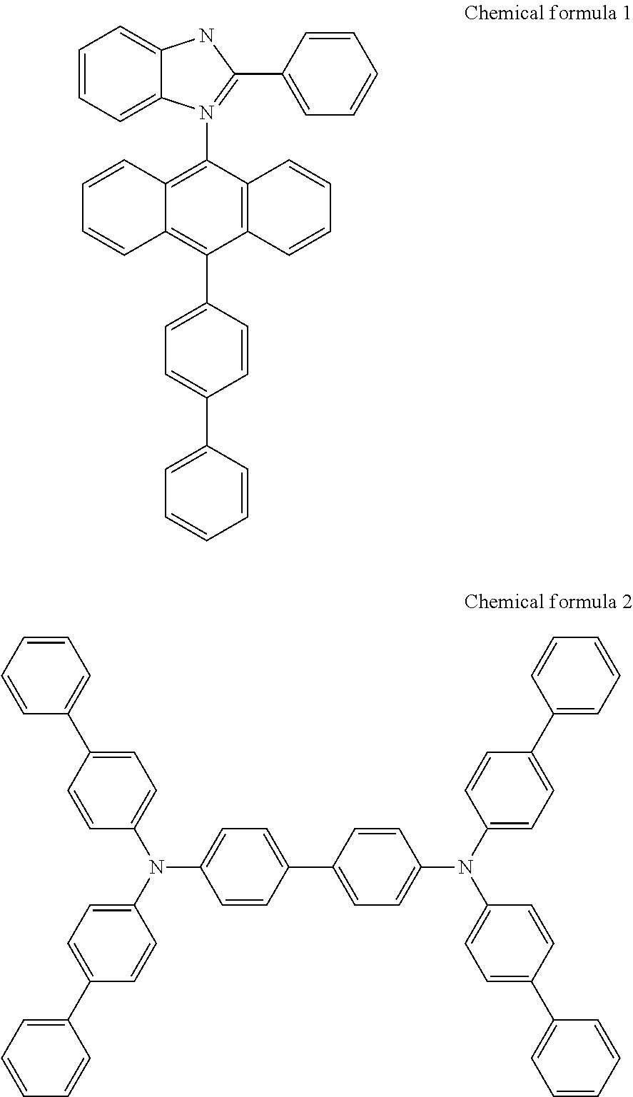

Priority Applications (2)
| Application Number | Priority Date | Filing Date | Title |
|---|---|---|---|
| US13/422,845 US20120175601A1 (en) | 2009-10-22 | 2012-03-16 | Display unit |
| US13/622,113 US20130015476A1 (en) | 2009-10-22 | 2012-09-18 | Display unit |
Applications Claiming Priority (2)
| Application Number | Priority Date | Filing Date | Title |
|---|---|---|---|
| JPP2009-243689 | 2009-10-22 | ||
| JP2009243689A JP5609058B2 (en) | 2009-10-22 | 2009-10-22 | Display device |
Related Child Applications (2)
| Application Number | Title | Priority Date | Filing Date |
|---|---|---|---|
| US13/422,845 Division US20120175601A1 (en) | 2009-10-22 | 2012-03-16 | Display unit |
| US13/622,113 Continuation US20130015476A1 (en) | 2009-10-22 | 2012-09-18 | Display unit |
Publications (2)
| Publication Number | Publication Date |
|---|---|
| US20110095276A1 true US20110095276A1 (en) | 2011-04-28 |
| US8294143B2 US8294143B2 (en) | 2012-10-23 |
Family
ID=43897627
Family Applications (3)
| Application Number | Title | Priority Date | Filing Date |
|---|---|---|---|
| US12/899,133 Active 2030-12-08 US8294143B2 (en) | 2009-10-22 | 2010-10-06 | Display unit including a multlayer structure |
| US13/422,845 Abandoned US20120175601A1 (en) | 2009-10-22 | 2012-03-16 | Display unit |
| US13/622,113 Abandoned US20130015476A1 (en) | 2009-10-22 | 2012-09-18 | Display unit |
Family Applications After (2)
| Application Number | Title | Priority Date | Filing Date |
|---|---|---|---|
| US13/422,845 Abandoned US20120175601A1 (en) | 2009-10-22 | 2012-03-16 | Display unit |
| US13/622,113 Abandoned US20130015476A1 (en) | 2009-10-22 | 2012-09-18 | Display unit |
Country Status (3)
| Country | Link |
|---|---|
| US (3) | US8294143B2 (en) |
| JP (1) | JP5609058B2 (en) |
| CN (1) | CN102097449B (en) |
Cited By (29)
| Publication number | Priority date | Publication date | Assignee | Title |
|---|---|---|---|---|
| US20120025225A1 (en) * | 2010-07-27 | 2012-02-02 | Seiko Epson Corporation | Light-emitting element, display device, and electronic apparatus |
| US20120267651A1 (en) * | 2011-04-25 | 2012-10-25 | Samsung Mobile Display Co., Ltd | Display device and method of manufacturing the same |
| US8410518B2 (en) * | 2011-06-10 | 2013-04-02 | Samsung Display Co., Ltd. | Organic light emitting diode display and method for manufacturing the same |
| CN103094308A (en) * | 2011-10-27 | 2013-05-08 | 乐金显示有限公司 | Organic electroluminescent display device |
| US20140077185A1 (en) * | 2012-09-19 | 2014-03-20 | Samsung Display Co., Ltd | Organic light emitting display |
| US20140124765A1 (en) * | 2011-01-25 | 2014-05-08 | Sony Corporation | Organic el display device and electronic apparatus |
| US20140209888A1 (en) * | 2013-01-18 | 2014-07-31 | Universal Display Corporation | High resolution low power consumption oled display with extended lifetime |
| GB2510690A (en) * | 2012-12-18 | 2014-08-13 | Lg Display Co Ltd | White organic light emitting device |
| US20150048328A1 (en) * | 2013-05-29 | 2015-02-19 | Sony Corporation | Display unit, method of manufacturing display unit, and electronic apparatus |
| US20160027849A1 (en) * | 2011-03-04 | 2016-01-28 | Semiconductor Energy Laboratory Co., Ltd. | Display Device |
| US20160163771A1 (en) * | 2014-12-08 | 2016-06-09 | Lg Display Co., Ltd. | Organic light emitting display device |
| US9385168B2 (en) | 2013-01-18 | 2016-07-05 | Universal Display Corporation | High resolution low power consumption OLED display with extended lifetime |
| US9424772B2 (en) | 2013-01-18 | 2016-08-23 | Universal Display Corporation | High resolution low power consumption OLED display with extended lifetime |
| US20170207281A1 (en) | 2013-01-18 | 2017-07-20 | Universal Display Corporation | High resolution low power consumption oled display with extended lifetime |
| US9818804B2 (en) | 2015-09-18 | 2017-11-14 | Universal Display Corporation | Hybrid display |
| US20170345875A1 (en) * | 2016-05-25 | 2017-11-30 | Samsung Display Co., Ltd. | Organic light emitting display |
| WO2018233353A1 (en) * | 2017-06-20 | 2018-12-27 | 京东方科技集团股份有限公司 | Organic light-emitting diode display panel and manufacturing method therefor, and display apparatus |
| US10229956B2 (en) | 2013-01-18 | 2019-03-12 | Universal Display Corporation | High resolution low power consumption OLED display with extended lifetime |
| US10243023B2 (en) | 2013-01-18 | 2019-03-26 | Universal Display Corporation | Top emission AMOLED displays using two emissive layers |
| US10263050B2 (en) | 2015-09-18 | 2019-04-16 | Universal Display Corporation | Hybrid display |
| US10539849B2 (en) | 2014-03-26 | 2020-01-21 | Joled Inc. | Color change member, light emitting device, display device and electronic apparatus |
| US10580832B2 (en) | 2013-01-18 | 2020-03-03 | Universal Display Corporation | High resolution low power consumption OLED display with extended lifetime |
| US10686159B2 (en) | 2015-06-26 | 2020-06-16 | Universal Display Corporation | OLED devices having improved efficiency |
| US10700134B2 (en) | 2014-05-27 | 2020-06-30 | Universal Display Corporation | Low power consumption OLED display |
| US10756141B2 (en) | 2016-07-28 | 2020-08-25 | Universal Display Corporation | Very high resolution stacked OLED display |
| US10797112B2 (en) | 2018-07-25 | 2020-10-06 | Universal Display Corporation | Energy efficient OLED TV |
| US20210273023A1 (en) * | 2018-06-29 | 2021-09-02 | Semiconductor Energy Laboratory Co., Ltd. | Display Panel, Display Device, Input/output Device, Data Processing Device |
| DE102013022617B3 (en) | 2012-12-18 | 2021-11-18 | Lg Display Co., Ltd. | White organic light emitting device and organic light emitting device |
| US20220158113A1 (en) * | 2020-11-18 | 2022-05-19 | Samsung Display Co., Ltd. | Display apparatus |
Families Citing this family (19)
| Publication number | Priority date | Publication date | Assignee | Title |
|---|---|---|---|---|
| JP5803648B2 (en) * | 2011-12-16 | 2015-11-04 | セイコーエプソン株式会社 | LIGHT EMITTING ELEMENT, LIGHT EMITTING DEVICE, DISPLAY DEVICE, AND ELECTRONIC DEVICE |
| US9793444B2 (en) * | 2012-04-06 | 2017-10-17 | Semiconductor Energy Laboratory Co., Ltd. | Display device and electronic device |
| US9711110B2 (en) * | 2012-04-06 | 2017-07-18 | Semiconductor Energy Laboratory Co., Ltd. | Display device comprising grayscale conversion portion and display portion |
| TW201403905A (en) * | 2012-06-01 | 2014-01-16 | Sony Corp | Organic electroluminescence device, manufacturing method thereof, and electronic equipment |
| KR101941453B1 (en) * | 2012-09-28 | 2019-01-23 | 엘지디스플레이 주식회사 | Organic light emitting display device |
| JP2014170091A (en) | 2013-03-04 | 2014-09-18 | Sony Corp | Display device, display driving method, method for manufacturing display device, and electronic apparatus |
| JP2015138746A (en) * | 2014-01-24 | 2015-07-30 | ソニー株式会社 | Organic el element, display device, and lighting device |
| CN103996696A (en) * | 2014-05-09 | 2014-08-20 | 京东方科技集团股份有限公司 | OLED display panel, manufacturing method of OLED display panel and display device |
| JP6528370B2 (en) * | 2014-07-25 | 2019-06-12 | セイコーエプソン株式会社 | Light emitting device and electronic device |
| CN104133320A (en) * | 2014-08-20 | 2014-11-05 | 深圳市华星光电技术有限公司 | Color liquid crystal display module structure and backlight module thereof |
| JP2016072250A (en) * | 2014-09-30 | 2016-05-09 | 株式会社半導体エネルギー研究所 | Light-emitting device, electronic equipment, and lighting device |
| JP2016085969A (en) | 2014-10-24 | 2016-05-19 | 株式会社半導体エネルギー研究所 | Light emitting element, light emitting device, electronic apparatus and lighting device |
| JP6517597B2 (en) * | 2015-06-10 | 2019-05-22 | 株式会社ジャパンディスプレイ | Display device |
| WO2020060283A1 (en) * | 2018-09-20 | 2020-03-26 | 주식회사 엘지화학 | Organic light emitting diode |
| JP6673997B2 (en) * | 2018-09-28 | 2020-04-01 | 株式会社Joled | Light emitting device, display device and electronic equipment |
| CN111100072A (en) * | 2019-11-28 | 2020-05-05 | 吉林奥来德光电材料股份有限公司 | Organic photoelectric compound, synthetic method thereof and organic electroluminescent device |
| JP2021179491A (en) * | 2020-05-12 | 2021-11-18 | セイコーエプソン株式会社 | Electrooptical device and electronic apparatus |
| JP7494555B2 (en) | 2020-05-14 | 2024-06-04 | セイコーエプソン株式会社 | Electro-optical devices and electronic equipment |
| CN117796146A (en) * | 2021-07-09 | 2024-03-29 | 索尼半导体解决方案公司 | Light emitting device and electronic apparatus |
Citations (1)
| Publication number | Priority date | Publication date | Assignee | Title |
|---|---|---|---|---|
| US20060082295A1 (en) * | 2004-10-18 | 2006-04-20 | Byung-Doo Chin | Full-color organic light emitting display having red, green, blue, cyan, magenta, and yellow color modulation layers |
Family Cites Families (7)
| Publication number | Priority date | Publication date | Assignee | Title |
|---|---|---|---|---|
| JP4094919B2 (en) * | 2002-07-18 | 2008-06-04 | 東北パイオニア株式会社 | Organic light emitting display |
| JP4635551B2 (en) * | 2004-10-06 | 2011-02-23 | ソニー株式会社 | Color liquid crystal display device |
| US7560862B2 (en) * | 2004-10-22 | 2009-07-14 | Eastman Kodak Company | White OLEDs with a color-compensated electroluminescent unit |
| JP4797438B2 (en) * | 2005-05-17 | 2011-10-19 | ソニー株式会社 | Organic electroluminescence device and display device |
| US7602119B2 (en) * | 2005-04-25 | 2009-10-13 | Eastman Kodak Company | OLED with magenta and green emissive layers |
| US7564182B2 (en) * | 2005-06-29 | 2009-07-21 | Eastman Kodak Company | Broadband light tandem OLED display |
| JP2009048829A (en) * | 2007-08-17 | 2009-03-05 | Seiko Epson Corp | Organic el white light-emitting panel, and electronic equipment |
-
2009
- 2009-10-22 JP JP2009243689A patent/JP5609058B2/en active Active
-
2010
- 2010-10-06 US US12/899,133 patent/US8294143B2/en active Active
- 2010-10-15 CN CN201010517397.3A patent/CN102097449B/en active Active
-
2012
- 2012-03-16 US US13/422,845 patent/US20120175601A1/en not_active Abandoned
- 2012-09-18 US US13/622,113 patent/US20130015476A1/en not_active Abandoned
Patent Citations (1)
| Publication number | Priority date | Publication date | Assignee | Title |
|---|---|---|---|---|
| US20060082295A1 (en) * | 2004-10-18 | 2006-04-20 | Byung-Doo Chin | Full-color organic light emitting display having red, green, blue, cyan, magenta, and yellow color modulation layers |
Cited By (67)
| Publication number | Priority date | Publication date | Assignee | Title |
|---|---|---|---|---|
| US8436374B2 (en) * | 2010-07-27 | 2013-05-07 | Seiko Epson Corporation | Light-emitting element, display device, and electronic apparatus |
| US20120025225A1 (en) * | 2010-07-27 | 2012-02-02 | Seiko Epson Corporation | Light-emitting element, display device, and electronic apparatus |
| US8987760B2 (en) * | 2011-01-25 | 2015-03-24 | Sony Corporation | Organic EL display device and electronic apparatus |
| US20140124765A1 (en) * | 2011-01-25 | 2014-05-08 | Sony Corporation | Organic el display device and electronic apparatus |
| US9673264B2 (en) * | 2011-03-04 | 2017-06-06 | Semiconductor Energy Laboratory Co., Ltd. | Display device |
| US20160027849A1 (en) * | 2011-03-04 | 2016-01-28 | Semiconductor Energy Laboratory Co., Ltd. | Display Device |
| US10153332B2 (en) | 2011-03-04 | 2018-12-11 | Semiconductor Energy Laboratory Co., Ltd. | Display device |
| US20120267651A1 (en) * | 2011-04-25 | 2012-10-25 | Samsung Mobile Display Co., Ltd | Display device and method of manufacturing the same |
| US9123670B2 (en) * | 2011-04-25 | 2015-09-01 | Samsung Display Co., Ltd. | Display device and method of manufacturing the same |
| US8410518B2 (en) * | 2011-06-10 | 2013-04-02 | Samsung Display Co., Ltd. | Organic light emitting diode display and method for manufacturing the same |
| CN103094308A (en) * | 2011-10-27 | 2013-05-08 | 乐金显示有限公司 | Organic electroluminescent display device |
| US9040979B2 (en) | 2011-10-27 | 2015-05-26 | Lg Display Co., Ltd. | Organic electroluminescent display device |
| US9048204B2 (en) | 2011-10-27 | 2015-06-02 | Lg Display Co., Ltd. | Organic electroluminescent display device |
| CN103681747A (en) * | 2012-09-19 | 2014-03-26 | 三星显示有限公司 | Organic light emitting display |
| US20140077185A1 (en) * | 2012-09-19 | 2014-03-20 | Samsung Display Co., Ltd | Organic light emitting display |
| US9337448B2 (en) * | 2012-09-19 | 2016-05-10 | Samsung Display Co., Ltd. | Organic light emitting display |
| US10741781B2 (en) | 2012-12-18 | 2020-08-11 | Lg Display Co., Ltd. | White organic light emitting device |
| US10418577B2 (en) | 2012-12-18 | 2019-09-17 | Lg Display Co., Ltd. | White organic light emitting device |
| US9224967B2 (en) | 2012-12-18 | 2015-12-29 | Lg Display Co., Ltd. | White organic light emitting device |
| DE102013022617B3 (en) | 2012-12-18 | 2021-11-18 | Lg Display Co., Ltd. | White organic light emitting device and organic light emitting device |
| GB2510690A (en) * | 2012-12-18 | 2014-08-13 | Lg Display Co Ltd | White organic light emitting device |
| DE102013112602B4 (en) * | 2012-12-18 | 2020-11-12 | Lg Display Co., Ltd. | White organic light emitting device |
| US10026915B2 (en) | 2012-12-18 | 2018-07-17 | Lg Display Co., Ltd. | White organic light emitting device |
| US20170092699A1 (en) * | 2013-01-18 | 2017-03-30 | Universal Display Corporation | High resolution low power consumption oled display with extended lifetime |
| US11302749B2 (en) | 2013-01-18 | 2022-04-12 | Universal Display Corporation | High resolution low power consumption OLED display with extended lifetime |
| US20170207281A1 (en) | 2013-01-18 | 2017-07-20 | Universal Display Corporation | High resolution low power consumption oled display with extended lifetime |
| US20140209888A1 (en) * | 2013-01-18 | 2014-07-31 | Universal Display Corporation | High resolution low power consumption oled display with extended lifetime |
| US11621300B2 (en) | 2013-01-18 | 2023-04-04 | Universal Display Corporation | High resolution low power consumption OLED display with extended lifetime |
| US11049907B2 (en) | 2013-01-18 | 2021-06-29 | Universal Display Corporation | High resolution low power consumption OLED display with extended lifetime |
| US10580832B2 (en) | 2013-01-18 | 2020-03-03 | Universal Display Corporation | High resolution low power consumption OLED display with extended lifetime |
| US9590017B2 (en) * | 2013-01-18 | 2017-03-07 | Universal Display Corporation | High resolution low power consumption OLED display with extended lifetime |
| US9424772B2 (en) | 2013-01-18 | 2016-08-23 | Universal Display Corporation | High resolution low power consumption OLED display with extended lifetime |
| US9385168B2 (en) | 2013-01-18 | 2016-07-05 | Universal Display Corporation | High resolution low power consumption OLED display with extended lifetime |
| US11450713B2 (en) | 2013-01-18 | 2022-09-20 | Universal Display Corporation | High resolution low power consumption OLED display with extended lifetime |
| US10229956B2 (en) | 2013-01-18 | 2019-03-12 | Universal Display Corporation | High resolution low power consumption OLED display with extended lifetime |
| US10243023B2 (en) | 2013-01-18 | 2019-03-26 | Universal Display Corporation | Top emission AMOLED displays using two emissive layers |
| US10374017B2 (en) * | 2013-01-18 | 2019-08-06 | Universal Display Corporation | High resolution low power consumption OLED display with extended lifetime |
| US10304906B2 (en) | 2013-01-18 | 2019-05-28 | Universal Display Corporation | High resolution low power consumption OLED display with extended lifetime |
| US9236581B2 (en) * | 2013-05-29 | 2016-01-12 | Sony Corporation | Display unit, method of manufacturing display unit, and electronic apparatus |
| CN110323256A (en) * | 2013-05-29 | 2019-10-11 | 索尼公司 | Display unit, the method and electronic equipment for manufacturing display unit |
| TWI629779B (en) * | 2013-05-29 | 2018-07-11 | 日商新力股份有限公司 | Display unit, method of manufacturing display unit, and electronic apparatus |
| US20150048328A1 (en) * | 2013-05-29 | 2015-02-19 | Sony Corporation | Display unit, method of manufacturing display unit, and electronic apparatus |
| US10539849B2 (en) | 2014-03-26 | 2020-01-21 | Joled Inc. | Color change member, light emitting device, display device and electronic apparatus |
| US10700134B2 (en) | 2014-05-27 | 2020-06-30 | Universal Display Corporation | Low power consumption OLED display |
| US11502134B2 (en) | 2014-05-27 | 2022-11-15 | Universal Display Corporation | Low power consumption OLED display |
| US20160163771A1 (en) * | 2014-12-08 | 2016-06-09 | Lg Display Co., Ltd. | Organic light emitting display device |
| US10950665B2 (en) | 2014-12-08 | 2021-03-16 | Lg Display Co., Ltd. | Organic light emitting display device |
| US11770955B2 (en) | 2014-12-08 | 2023-09-26 | Lg Display Co., Ltd. | Organic light emitting display device |
| US10686159B2 (en) | 2015-06-26 | 2020-06-16 | Universal Display Corporation | OLED devices having improved efficiency |
| US11121346B2 (en) | 2015-06-26 | 2021-09-14 | Universal Display Corporation | OLED devices having improved efficiency |
| US10128319B2 (en) | 2015-09-18 | 2018-11-13 | Universal Display Corporation | Hybrid display |
| US10263050B2 (en) | 2015-09-18 | 2019-04-16 | Universal Display Corporation | Hybrid display |
| US9818804B2 (en) | 2015-09-18 | 2017-11-14 | Universal Display Corporation | Hybrid display |
| US20170345875A1 (en) * | 2016-05-25 | 2017-11-30 | Samsung Display Co., Ltd. | Organic light emitting display |
| US10340315B2 (en) * | 2016-05-25 | 2019-07-02 | Samsung Display Co., Ltd. | Organic light emitting display with color filter layers |
| CN107437588A (en) * | 2016-05-25 | 2017-12-05 | 三星显示有限公司 | Oganic light-emitting display device and its manufacture method |
| US10756141B2 (en) | 2016-07-28 | 2020-08-25 | Universal Display Corporation | Very high resolution stacked OLED display |
| US11183541B2 (en) | 2016-07-28 | 2021-11-23 | Universal Display Corporation | Very high resolution stacked OLED display |
| US11189811B2 (en) | 2017-06-20 | 2021-11-30 | Boe Technology Group Co., Ltd. | Organic light emitting diode display panel having wide color gamut and low power consumption, manufacturing method thereof, and display device |
| WO2018233353A1 (en) * | 2017-06-20 | 2018-12-27 | 京东方科技集团股份有限公司 | Organic light-emitting diode display panel and manufacturing method therefor, and display apparatus |
| US11985881B2 (en) * | 2018-06-29 | 2024-05-14 | Semiconductor Energy Laboratory Co., Ltd. | Display panel, display device, input/output device, data processing device |
| US20210273023A1 (en) * | 2018-06-29 | 2021-09-02 | Semiconductor Energy Laboratory Co., Ltd. | Display Panel, Display Device, Input/output Device, Data Processing Device |
| US11700756B2 (en) | 2018-07-25 | 2023-07-11 | Universal Display Corporation | Energy efficient OLED TV |
| US10964757B2 (en) | 2018-07-25 | 2021-03-30 | Universal Display Corporation | Energy efficient OLED TV |
| US11839124B2 (en) | 2018-07-25 | 2023-12-05 | Universal Display Corporation | Energy efficient OLED TV |
| US10797112B2 (en) | 2018-07-25 | 2020-10-06 | Universal Display Corporation | Energy efficient OLED TV |
| US20220158113A1 (en) * | 2020-11-18 | 2022-05-19 | Samsung Display Co., Ltd. | Display apparatus |
Also Published As
| Publication number | Publication date |
|---|---|
| US8294143B2 (en) | 2012-10-23 |
| JP5609058B2 (en) | 2014-10-22 |
| JP2011090894A (en) | 2011-05-06 |
| CN102097449A (en) | 2011-06-15 |
| US20120175601A1 (en) | 2012-07-12 |
| US20130015476A1 (en) | 2013-01-17 |
| CN102097449B (en) | 2014-10-22 |
Similar Documents
| Publication | Publication Date | Title |
|---|---|---|
| US8294143B2 (en) | Display unit including a multlayer structure | |
| CN109076674B (en) | Display device and method for manufacturing the same | |
| US8471275B2 (en) | Organic light emitting device display and method of manufacturing the same | |
| US8878206B2 (en) | Organic light emitting display apparatus including an auxiliary layer and method for manufacturing the same | |
| US7541734B2 (en) | Light emitting device having a layer with a metal oxide and a benzoxazole derivative | |
| US9252379B2 (en) | Organic light emitting device | |
| JP6538271B2 (en) | Display device and method of manufacturing the same | |
| KR102604311B1 (en) | Organic Light Emitting Device, Organic Light Emitting Display Device and Vehicle Mounted Display Using the Same | |
| JP5094477B2 (en) | Organic light-emitting display device and method for manufacturing the same | |
| CN109791994B (en) | Display device and method for manufacturing the same | |
| US10115924B2 (en) | Organic light emitting display apparatus | |
| US8716931B2 (en) | Organic light emitting diode (OLED) display | |
| JP2007299729A (en) | Organic el display device | |
| JPWO2018070348A1 (en) | Display device and manufacturing method thereof | |
| US10483328B2 (en) | Organic light-emitting element and organic light-emitting display device | |
| US10205113B2 (en) | Organic electroluminescence device including an emissive layer including an assistant dopant layer and light-emitting dopant layer | |
| KR101279121B1 (en) | Organic Light Emitting Display Device | |
| JP2006302879A (en) | Light emitting element, light emitting device equipped with light emitting element, and its manufacturing method | |
| JP5256831B2 (en) | Display element, display device, and method of manufacturing display element | |
| KR20200013901A (en) | Display device | |
| KR102113609B1 (en) | Organic light emitting display and manufactucring method of the same | |
| KR102367821B1 (en) | White Organic Light Emitting Device and Organic Light Emitting Display Device | |
| KR20110053568A (en) | Organic light emitting display device | |
| KR20170061441A (en) | Organic light emitting display apparatus |
Legal Events
| Date | Code | Title | Description |
|---|---|---|---|
| AS | Assignment |
Owner name: SONY CORPORATION, JAPAN Free format text: ASSIGNMENT OF ASSIGNORS INTEREST;ASSIGNORS:IMAI, TOSHIAKI;MATSUNAMI, SHIGEYUKI;KIJIMA, YASUNORI;SIGNING DATES FROM 20100906 TO 20100916;REEL/FRAME:025113/0649 |
|
| STCF | Information on status: patent grant |
Free format text: PATENTED CASE |
|
| FEPP | Fee payment procedure |
Free format text: PAYOR NUMBER ASSIGNED (ORIGINAL EVENT CODE: ASPN); ENTITY STATUS OF PATENT OWNER: LARGE ENTITY |
|
| AS | Assignment |
Owner name: JOLED INC., JAPAN Free format text: ASSIGNMENT OF ASSIGNORS INTEREST;ASSIGNOR:SONY CORPORATION;REEL/FRAME:036106/0355 Effective date: 20150618 |
|
| FPAY | Fee payment |
Year of fee payment: 4 |
|
| MAFP | Maintenance fee payment |
Free format text: PAYMENT OF MAINTENANCE FEE, 8TH YEAR, LARGE ENTITY (ORIGINAL EVENT CODE: M1552); ENTITY STATUS OF PATENT OWNER: LARGE ENTITY Year of fee payment: 8 |
|
| AS | Assignment |
Owner name: INCJ, LTD., JAPAN Free format text: SECURITY INTEREST;ASSIGNOR:JOLED, INC.;REEL/FRAME:063396/0671 Effective date: 20230112 |
|
| AS | Assignment |
Owner name: JOLED, INC., JAPAN Free format text: CORRECTION BY AFFIDAVIT FILED AGAINST REEL/FRAME 063396/0671;ASSIGNOR:JOLED, INC.;REEL/FRAME:064067/0723 Effective date: 20230425 |
|
| AS | Assignment |
Owner name: JDI DESIGN AND DEVELOPMENT G.K., JAPAN Free format text: ASSIGNMENT OF ASSIGNORS INTEREST;ASSIGNOR:JOLED, INC.;REEL/FRAME:066382/0619 Effective date: 20230714 |
|
| MAFP | Maintenance fee payment |
Free format text: PAYMENT OF MAINTENANCE FEE, 12TH YEAR, LARGE ENTITY (ORIGINAL EVENT CODE: M1553); ENTITY STATUS OF PATENT OWNER: LARGE ENTITY Year of fee payment: 12 |