JP2019117941A - Electro-optical device - Google Patents
Electro-optical device Download PDFInfo
- Publication number
- JP2019117941A JP2019117941A JP2019050965A JP2019050965A JP2019117941A JP 2019117941 A JP2019117941 A JP 2019117941A JP 2019050965 A JP2019050965 A JP 2019050965A JP 2019050965 A JP2019050965 A JP 2019050965A JP 2019117941 A JP2019117941 A JP 2019117941A
- Authority
- JP
- Japan
- Prior art keywords
- pixel
- sub
- light emitting
- distance
- certain
- Prior art date
- Legal status (The legal status is an assumption and is not a legal conclusion. Google has not performed a legal analysis and makes no representation as to the accuracy of the status listed.)
- Pending
Links
- 230000008859 change Effects 0.000 abstract description 58
- 101100494448 Caenorhabditis elegans cab-1 gene Proteins 0.000 abstract description 4
- 230000001965 increasing effect Effects 0.000 abstract description 4
- 239000010410 layer Substances 0.000 description 123
- 230000004048 modification Effects 0.000 description 60
- 238000012986 modification Methods 0.000 description 60
- 239000000758 substrate Substances 0.000 description 28
- 238000007789 sealing Methods 0.000 description 13
- 239000002346 layers by function Substances 0.000 description 11
- 230000004888 barrier function Effects 0.000 description 10
- 229910052751 metal Inorganic materials 0.000 description 10
- 239000002184 metal Substances 0.000 description 10
- 230000001681 protective effect Effects 0.000 description 10
- 239000010408 film Substances 0.000 description 9
- 239000003990 capacitor Substances 0.000 description 8
- 238000000926 separation method Methods 0.000 description 8
- 230000003287 optical effect Effects 0.000 description 7
- VYPSYNLAJGMNEJ-UHFFFAOYSA-N silicon dioxide Inorganic materials O=[Si]=O VYPSYNLAJGMNEJ-UHFFFAOYSA-N 0.000 description 7
- 239000011241 protective layer Substances 0.000 description 6
- 239000000203 mixture Substances 0.000 description 5
- 229910052814 silicon oxide Inorganic materials 0.000 description 5
- 239000012790 adhesive layer Substances 0.000 description 4
- 239000003086 colorant Substances 0.000 description 4
- 238000010586 diagram Methods 0.000 description 4
- 230000002708 enhancing effect Effects 0.000 description 4
- 239000011810 insulating material Substances 0.000 description 4
- 239000011229 interlayer Substances 0.000 description 4
- 239000010936 titanium Substances 0.000 description 4
- 230000009467 reduction Effects 0.000 description 3
- 229920005989 resin Polymers 0.000 description 3
- 239000011347 resin Substances 0.000 description 3
- 101100379376 Caenorhabditis elegans apx-1 gene Proteins 0.000 description 2
- 229910052581 Si3N4 Inorganic materials 0.000 description 2
- XUIMIQQOPSSXEZ-UHFFFAOYSA-N Silicon Chemical compound [Si] XUIMIQQOPSSXEZ-UHFFFAOYSA-N 0.000 description 2
- RTAQQCXQSZGOHL-UHFFFAOYSA-N Titanium Chemical compound [Ti] RTAQQCXQSZGOHL-UHFFFAOYSA-N 0.000 description 2
- 239000000956 alloy Substances 0.000 description 2
- 229910045601 alloy Inorganic materials 0.000 description 2
- 239000010949 copper Substances 0.000 description 2
- 230000000694 effects Effects 0.000 description 2
- 239000003822 epoxy resin Substances 0.000 description 2
- 230000005669 field effect Effects 0.000 description 2
- 229920000647 polyepoxide Polymers 0.000 description 2
- 239000010453 quartz Substances 0.000 description 2
- 229910052710 silicon Inorganic materials 0.000 description 2
- 239000010703 silicon Substances 0.000 description 2
- HQVNEWCFYHHQES-UHFFFAOYSA-N silicon nitride Chemical compound N12[Si]34N5[Si]62N3[Si]51N64 HQVNEWCFYHHQES-UHFFFAOYSA-N 0.000 description 2
- 229910052719 titanium Inorganic materials 0.000 description 2
- -1 81: color filter Substances 0.000 description 1
- 229910016570 AlCu Inorganic materials 0.000 description 1
- 101100109216 Caenorhabditis elegans apy-1 gene Proteins 0.000 description 1
- RYGMFSIKBFXOCR-UHFFFAOYSA-N Copper Chemical compound [Cu] RYGMFSIKBFXOCR-UHFFFAOYSA-N 0.000 description 1
- 229910004298 SiO 2 Inorganic materials 0.000 description 1
- NRTOMJZYCJJWKI-UHFFFAOYSA-N Titanium nitride Chemical compound [Ti]#N NRTOMJZYCJJWKI-UHFFFAOYSA-N 0.000 description 1
- 230000009471 action Effects 0.000 description 1
- 229910052782 aluminium Inorganic materials 0.000 description 1
- XAGFODPZIPBFFR-UHFFFAOYSA-N aluminium Chemical compound [Al] XAGFODPZIPBFFR-UHFFFAOYSA-N 0.000 description 1
- QVGXLLKOCUKJST-UHFFFAOYSA-N atomic oxygen Chemical compound [O] QVGXLLKOCUKJST-UHFFFAOYSA-N 0.000 description 1
- 239000004020 conductor Substances 0.000 description 1
- 230000008094 contradictory effect Effects 0.000 description 1
- 229910052802 copper Inorganic materials 0.000 description 1
- 230000006866 deterioration Effects 0.000 description 1
- 239000011521 glass Substances 0.000 description 1
- 230000005525 hole transport Effects 0.000 description 1
- AMGQUBHHOARCQH-UHFFFAOYSA-N indium;oxotin Chemical compound [In].[Sn]=O AMGQUBHHOARCQH-UHFFFAOYSA-N 0.000 description 1
- 238000002347 injection Methods 0.000 description 1
- 239000007924 injection Substances 0.000 description 1
- 229910010272 inorganic material Inorganic materials 0.000 description 1
- 239000011147 inorganic material Substances 0.000 description 1
- 239000000463 material Substances 0.000 description 1
- 238000001579 optical reflectometry Methods 0.000 description 1
- 229910052760 oxygen Inorganic materials 0.000 description 1
- 239000001301 oxygen Substances 0.000 description 1
- 238000005192 partition Methods 0.000 description 1
- 230000035515 penetration Effects 0.000 description 1
- 230000002093 peripheral effect Effects 0.000 description 1
- 239000000049 pigment Substances 0.000 description 1
- 239000004065 semiconductor Substances 0.000 description 1
- 229910052709 silver Inorganic materials 0.000 description 1
- 239000010409 thin film Substances 0.000 description 1
- 230000009466 transformation Effects 0.000 description 1
- 239000012780 transparent material Substances 0.000 description 1
- WFKWXMTUELFFGS-UHFFFAOYSA-N tungsten Chemical compound [W] WFKWXMTUELFFGS-UHFFFAOYSA-N 0.000 description 1
- 229910052721 tungsten Inorganic materials 0.000 description 1
- 239000010937 tungsten Substances 0.000 description 1
Images


Abstract
Description
本発明は、電気光学装置に関する。 The present invention relates to an electro-optical device.
有機EL(electro luminescent)素子等の発光素子を含む電気光学装置において、カラー表示を実現するために、発光素子を覆う封止層の上に、所望の波長領域の光を透過するカラーフィルターが設けられた構成が知られている。また、このような電気光学装置では、一般的には、複数のサブ画素から構成される画素により1つの表示単位が形成される。また、電気光学装置に設けられるサブ画素は、発光領域を有する発光素子と、発光素子に供給する電力を出力する供給回路と、供給回路と発光素子とを電気的に接続するコンタクト領域と、を備える。例えば、特許文献1には、赤色、緑色、青色の3原色のサブ画素によって、1つの画素を形成した電気光学装置が開示されている。この電気光学装置には、コンタクト領域を介して発光素子と供給回路とが電気的に接続することが開示されている。
In an electro-optical device including a light emitting element such as an organic EL (electro luminescent) element, in order to realize color display, a color filter for transmitting light in a desired wavelength region is provided on a sealing layer covering the light emitting element. Configurations are known. In addition, in such an electro-optical device, generally, one display unit is formed by pixels configured by a plurality of sub-pixels. In addition, a sub-pixel provided in the electro-optical device includes a light-emitting element having a light-emitting area, a supply circuit that outputs power supplied to the light-emitting element, and a contact area that electrically connects the supply circuit and the light-emitting element. Prepare. For example,
ところで、サブ画素の配置は、発光素子を大きくして開口率が高くなるように設計されている。従って、発光素子は、可能な限り大きくして配置されることになる。しかしながら、可能な限り大きくして配置された発光素子の間にコンタクト領域が設けられることによって、上述した従来の電気光学装置では、コンタクト領域を介してサブ画素の発光素子同士が隣り合う箇所と、コンタクト領域を介さずにサブ画素の発光素子同士が隣り合う箇所とが発生する。従って、各発光素子上に各カラーフィルターが配置される場合、あるサブ画素の発光素子と、あるサブ画素に対して隣り合うカラーフィルターとの距離が、サブ画素間でそれぞれ異なることになる。
前述した距離がサブ画素間でそれぞれ異なると、ある視野角について、あるサブ画素の発光素子から射出された光が、前述のあるサブ画素に隣り合うカラーフィルターを透過して色変化が発生した際に、別のサブ画素の発光素子から射出された光は、前述の別のサブ画素に隣り合うカラーフィルターを透過せずに色変化が発生しない状況が起こり得る。このように、あるサブ画素の発光素子と、あるサブ画素に対して隣り合うカラーフィルターとの距離が、サブ画素間でそれぞれ異なると、視野角による色変化のばらつきが発生するという問題がある。
By the way, the arrangement of the sub-pixels is designed to increase the aperture ratio by enlarging the light emitting element. Therefore, the light emitting elements are arranged as large as possible. However, by providing the contact region between the light emitting elements arranged as large as possible, in the above-described conventional electro-optical device, the light emitting elements of the sub-pixels are adjacent to each other via the contact region; The light emitting elements of the sub-pixels are adjacent to each other without passing through the contact region. Therefore, when each color filter is disposed on each light emitting element, the distance between the light emitting element of a certain sub pixel and the color filter adjacent to a certain sub pixel is different between the sub pixels.
When the distances described above are different between sub-pixels, when a light emitted from a light-emitting element of a certain sub-pixel transmits a color filter adjacent to a certain sub-pixel at a certain viewing angle, a color change occurs In addition, light emitted from the light emitting element of another sub-pixel may not pass through the color filter adjacent to the other sub-pixel and a color change may not occur. As described above, when the distance between the light emitting element of a certain sub-pixel and the color filter adjacent to a certain sub-pixel is different between the sub-pixels, there is a problem that variation in color change due to the viewing angle occurs.
本発明は、開口率を高くする場合であっても視野角による色変化のばらつきを抑えることを解決課題の一つとする。 The present invention addresses one of the problems to be solved by suppressing the variation in color change due to the viewing angle even when the aperture ratio is increased.
本発明の一態様に係る電気光学装置は、第1の方向と前記第1の方向に交差する第2の方向に沿って配列された複数の画素を備え、前記複数の画素の各々は、前記第1の方向に沿って配置された第1のサブ画素および第2のサブ画素と、前記第1の方向に沿って配置された第4のサブ画素および第3のサブ画素とを備え、前記第4のサブ画素および前記第1のサブ画素は、前記第2の方向に沿って配置され、前記第3のサブ画素および前記第2のサブ画素は、前記第2の方向に沿って配置され、前記第1のサブ画素、前記第2のサブ画素、前記第3のサブ画素、および前記第4のサブ画素の各々に対応するカラーフィルターを備え、前記第1のサブ画素、前記第2のサブ画素、前記第3のサブ画素、および前記第4のサブ画素の各々は、発光領域を有する発光素子と、前記発光素子に供給する電流を出力する供給回路と、前記発光素子と前記供給回路とを電気的に接続するコンタクトが配置されるコンタクト領域を備え、前記コンタクト領域は、前記第1のサブ画素、前記第2のサブ画素、前記第3のサブ画素、および前記第4のサブ画素の各々に設けられた前記発光領域を区分けする境界線の交点と重なる、ことを特徴とする。 An electro-optical device according to an aspect of the present invention includes a plurality of pixels arranged along a second direction crossing a first direction and the first direction, each of the plurality of pixels being A first sub-pixel and a second sub-pixel arranged along a first direction, and a fourth sub-pixel and a third sub-pixel arranged along the first direction, The fourth sub-pixel and the first sub-pixel are arranged along the second direction, and the third sub-pixel and the second sub-pixel are arranged along the second direction. A color filter corresponding to each of the first sub-pixel, the second sub-pixel, the third sub-pixel, and the fourth sub-pixel, the first sub-pixel, the second sub-pixel, Each of the sub-pixel, the third sub-pixel, and the fourth sub-pixel emits light A light emitting element having a light emitting area, a supply circuit for outputting a current supplied to the light emitting element, and a contact area in which a contact electrically connecting the light emitting element and the supply circuit is disposed, the contact area being The light emitting region is overlapped with an intersection point of the light emitting region provided in each of the first sub-pixel, the second sub-pixel, the third sub-pixel, and the fourth sub-pixel. I assume.
本発明の一態様によれば、各発光領域を区分けする境界線の交点は、各発光領域の中心から離れた位置にあるため、コンタクト領域を設けることによって発光領域が小さくなることを抑制することができる。さらに、コンタクト領域を交点と重なるように配置することにより、隣接する他のサブ画素の一部のエリアを使ってコンタクト領域を配置することができる。そして、あるサブ画素の一部のエリアおよび隣接する他のサブ画素の一部のエリアを使ってあるサブ画素のコンタクト領域を配置することは、境界線を跨ってコンタクト領域を配置することになる。以上により、コンタクト領域をサブ画素間で均等な間隔で配置することが可能になり、発光領域の間隔も一定となる。発光領域の間隔が一定となることにより、視野角による色変化のばらつきを抑えることが可能になる。このように、発光領域が小さくなることを抑制しつつ、視野角による色変化のばらつきを抑えることが可能になる。 According to one aspect of the present invention, since the intersections of the boundaries dividing the light emitting areas are at positions away from the centers of the light emitting areas, the provision of the contact areas suppresses the reduction of the light emitting areas. Can. Furthermore, by arranging the contact area so as to overlap the intersection, the contact area can be arranged using an area of a part of another adjacent sub-pixel. Then, arranging a contact region of a certain sub-pixel using a partial area of a certain sub-pixel and a partial area of another adjacent sub-pixel results in arranging a contact region across the border. . As described above, the contact regions can be arranged at equal intervals between the sub-pixels, and the intervals between the light emitting regions are also constant. When the distance between the light emitting regions is constant, it is possible to suppress the variation of the color change due to the viewing angle. As described above, it is possible to suppress the variation of the color change due to the viewing angle while suppressing the reduction of the light emitting region.
また、本発明の一態様に係る電気光学装置は、第1の方向と前記第1の方向に交差する第2の方向に沿って配列された複数の画素を備え、前記複数の画素の各々は、前記第1の方向に沿って配置された第1のサブ画素および第2のサブ画素と、前記第1の方向に沿って配置された第4のサブ画素および第3のサブ画素とを備え、前記第4のサブ画素および前記第1のサブ画素は、前記第2の方向に沿って配置され、前記第3のサブ画素および前記第2のサブ画素は、前記第2の方向に沿って配置され、前記第1のサブ画素、前記第2のサブ画素、前記第3のサブ画素、および前記第4のサブ画素の各々に対応するカラーフィルターを備え、前記第1のサブ画素、前記第2のサブ画素、前記第3のサブ画素、および前記第4のサブ画素の各々は、発光領域を有する発光素子と、前記発光素子に供給する電流を出力する供給回路と備え、前記発光領域の内側に、前記供給回路と前記発光素子とを電気的に接続するコンタクトが配置されるコンタクト領域を備える、ことを特徴としてもよい。 Further, an electro-optical device according to an aspect of the present invention includes a plurality of pixels arranged along a second direction crossing the first direction and the first direction, each of the plurality of pixels being A first sub-pixel and a second sub-pixel arranged along the first direction, and a fourth sub-pixel and a third sub-pixel arranged along the first direction The fourth sub-pixel and the first sub-pixel are disposed along the second direction, and the third sub-pixel and the second sub-pixel are disposed along the second direction. A color filter corresponding to each of the first sub-pixel, the second sub-pixel, the third sub-pixel, and the fourth sub-pixel; Each of the two sub-pixels, the third sub-pixel, and the fourth sub-pixel is A contact comprising: a light emitting element having a light emitting region; and a supply circuit for outputting a current supplied to the light emitting element, wherein a contact electrically connecting the supply circuit to the light emitting element is disposed inside the light emitting region. A region may be provided.
本発明の一態様によれば、発光領域の内側にコンタクト領域が配置されることにより、コンタクト領域が発光領域の外側には存在しないため、コンタクト領域の存在によって発光領域同士の間隔がばらつくことを発生しないようにすることが可能になる。従って、発光領域同士の間隔を均等にすることができるため、視野角による色変化のばらつきを抑えることが可能になる。 According to one aspect of the present invention, since the contact region is not present outside the light emitting region by arranging the contact region inside the light emitting region, the distance between the light emitting regions varies due to the presence of the contact region. It becomes possible not to occur. Therefore, since the intervals between the light emitting regions can be made uniform, it is possible to suppress the variation of the color change due to the viewing angle.
また、上述した態様によれば、ある画素における第1のサブ画素の発光領域と第2のサブ画素の発光領域との間の距離は、前記ある画素の第2のサブ画素の発光領域と当該ある画素に対して前記第1の方向に並ぶ画素における第1のサブ画素の発光領域との間の距離と略等しく、前記ある画素における第4のサブ画素の発光領域と第3のサブ画素の発光領域との間の距離は、前記ある画素の第3のサブ画素の発光領域と当該ある画素に対して前記第1の方向に並ぶ画素における第4のサブ画素の発光領域との間の距離と略等しい、ことが好ましい。 Further, according to the aspect described above, the distance between the light emitting area of the first sub-pixel and the light emitting area of the second sub-pixel in a certain pixel is the light emitting area of the second sub-pixel of the certain pixel The distance between the light emitting area of the fourth sub pixel in the pixel and the light emitting area of the third sub pixel is approximately equal to the distance between the light emitting area of the first sub pixel in the pixels aligned in the first direction The distance between the light emitting area and the light emitting area is the distance between the light emitting area of the third sub pixel of the certain pixel and the light emitting area of the fourth sub pixel in the pixel aligned in the first direction with respect to the certain pixel. Preferably, it is approximately equal to
この態様によれば、ある画素における第1のサブ画素の発光領域と第2のサブ画素の発光領域との間の距離が、前述の第2のサブ画素の発光領域と前述のある画素に対して第1の方向に並ぶ画素における第1のサブ画素の発光領域との間の距離と略等しいことにより、第1のサブ画素の発光領域と第1のサブ画素に対して第1の方向の隣に位置するカラーフィルター端部との距離と、第2のサブ画素の発光領域と第2のサブ画素に対して第1の方向の隣に位置するカラーフィルター端部の距離とが略等しいことになる。この2つの距離が略等しいことにより、第1の方向における色変化が、略同一の視野角で発生することになるため、第1の方向に沿って配置された発光領域間の距離のばらつきによって発生する、第1の方向の視野角による色変化のばらつきを抑えることが可能になる。 According to this aspect, the distance between the light emitting region of the first sub-pixel and the light emitting region of the second sub-pixel in a certain pixel is the distance between the light emitting region of the second sub-pixel and the certain pixel. The distance between the light emitting area of the first sub-pixel and the first sub-pixel in the first direction is approximately equal to the distance between the light emitting area of the first sub-pixel in the pixels aligned in the first direction. The distance between the color filter end located next to it and the distance between the light emitting area of the second sub-pixel and the color filter end located next to the second sub-pixel in the first direction are substantially equal become. Since the two distances are substantially equal, a color change in the first direction will occur at substantially the same viewing angle, and the variation in the distance between the light emitting regions arranged along the first direction It is possible to suppress the variation in color change due to the viewing angle in the first direction that occurs.
また、上述した態様によれば、ある画素における第1のサブ画素の発光領域と第4のサブ画素の発光領域との間の距離は、前記ある画素の第4のサブ画素の発光領域と当該ある画素に対して前記第2の方向に並ぶ画素における第1のサブ画素の発光領域との間の距離と略等しく、前記ある画素における第2のサブ画素の発光領域と第3のサブ画素の発光領域との間の距離は、前記ある画素の第3のサブ画素の発光領域と当該ある画素に対して前記第2の方向に並ぶ画素における第2のサブ画素の発光領域との間の距離と略等しい、ことが好ましい。 Further, according to the aspect described above, the distance between the light emitting area of the first sub-pixel and the light emitting area of the fourth sub-pixel in a certain pixel is the light emitting area of the fourth sub-pixel of the certain pixel The distance between the light emitting area of the second sub pixel in the pixel and the third sub pixel is approximately equal to the distance between the light emitting area of the first sub pixel in the pixels aligned in the second direction with respect to the certain pixel and the light emitting area The distance between the light emitting area and the light emitting area is the distance between the light emitting area of the third sub pixel of the certain pixel and the light emitting area of the second sub pixel in the pixel aligned in the second direction with respect to the certain pixel. Preferably, it is approximately equal to
この態様によれば、第1の方向と同様に、第2の方向に沿って配置された発光領域間の距離のばらつきによって発生する、第2の方向の視野角による色変化のばらつきを抑えることが可能になる。 According to this aspect, similarly to the first direction, it is possible to suppress the variation in the color change due to the viewing angle in the second direction, which is caused by the variation in the distance between the light emitting regions arranged along the second direction. Becomes possible.
また、上述した態様によれば、前記第1のサブ画素、前記第2のサブ画素、前記第3のサブ画素、および前記第4のサブ画素のうちあるサブ画素の色と、当該あるサブ画素に対して前記第1の方向に沿って配置されたサブ画素の色との関係は、前記あるサブ画素の色に応じて一意に定まる、ことが好ましい。 Further, according to the aspect described above, the color of a certain sub-pixel among the first sub-pixel, the second sub-pixel, the third sub-pixel, and the fourth sub-pixel, and the certain sub-pixel Preferably, the relationship with the color of the sub-pixel arranged along the first direction is uniquely determined according to the color of the certain sub-pixel.
一般に、同一の色のサブ画素同士に対して、ある方向に位置するカラーフィルターの色がばらついていると、ある方向における視野角によって色変化が発生した際に、同一の色のサブ画素から射出される光は、それぞれ異なる色変化を起こすことになり、視野角による色変化がばらつくことになる。一方、前述の態様によれば、あるサブ画素の色と、あるサブ画素に対して第1の方向に沿って配置されたサブ画素の色との関係が、あるサブ画素の色に応じて一意に定まることにより、同一の色のサブ画素に対して第1の方向に位置するカラーフィルターの色は、一意に定まる。従って、第1の方向において、ある視野角によって色変化が発生した際に、同一の色のサブ画素では、一意に定まった色変化が発生するため、第1の方向に位置するカラーフィルターの色のばらつきによって発生する、第1の方向の視野角による色変化のばらつきを抑えることができる。 Generally, when the color of the color filter located in a certain direction is different among the sub-pixels of the same color, when color change occurs due to the viewing angle in a certain direction, the light is emitted from the sub-pixel of the same color Each of the lights causes different color change, and the color change depending on the viewing angle is dispersed. On the other hand, according to the above aspect, the relationship between the color of a certain sub-pixel and the color of a sub-pixel arranged along the first direction with respect to a certain sub-pixel is unique according to the color of a certain sub-pixel Thus, the color of the color filter positioned in the first direction with respect to the sub-pixels of the same color is uniquely determined. Therefore, when a color change occurs due to a certain viewing angle in the first direction, a uniquely determined color change occurs in the sub-pixels of the same color, so the color of the color filter positioned in the first direction The variation in color change due to the viewing angle in the first direction, which is caused by the variation in.
また、上述した態様によれば、前記第1のサブ画素、前記第2のサブ画素、前記第3のサブ画素、および前記第4のサブ画素のうちあるサブ画素の色と、当該あるサブ画素に対して前記第2の方向に沿って配置されたサブ画素の色との関係は、前記あるサブ画素の色に応じて一意に定まる、ことが好ましい。 Further, according to the aspect described above, the color of a certain sub-pixel among the first sub-pixel, the second sub-pixel, the third sub-pixel, and the fourth sub-pixel, and the certain sub-pixel Preferably, the relationship with the color of the sub-pixel arranged along the second direction is uniquely determined in accordance with the color of the certain sub-pixel.
この態様によれば、第1の方向と同様に、第2の方向に位置するカラーフィルターの色のばらつきによって発生する、第2の方向の視野角による色変化のばらつきを抑えることができる。 According to this aspect, similarly to the first direction, it is possible to suppress the variation in color change due to the viewing angle in the second direction, which is caused by the variation in color of the color filter positioned in the second direction.
また、上述した態様によれば、前記第1の方向に対して第1の角度で傾き、かつ前記第2の方向に対して第2の角度で傾いた方向を第3の方向としたとき、前記コンタクト領域は、前記第3の方向に沿って並んでおり、前記第1のサブ画素、前記第2のサブ画素、前記第3のサブ画素、および前記第4のサブ画素の各々は、前記供給回路と電気的に接続された反射電極と、中間電極と、画素電極と、を備え、前記コンタクト領域には、前記反射電極と前記中間電極とを電気的に接続する第1のコンタクトと、前記中間電極と前記画素電極とを電気的に接続する第2のコンタクトとが配置される、ことが好ましい。 Further, according to the aspect described above, when a direction inclined at a first angle with respect to the first direction and inclined at a second angle with respect to the second direction is a third direction, The contact regions are arranged along the third direction, and each of the first sub-pixel, the second sub-pixel, the third sub-pixel, and the fourth sub-pixel is A reflective electrode electrically connected to the supply circuit, an intermediate electrode, and a pixel electrode, and the contact region includes a first contact electrically connecting the reflective electrode and the intermediate electrode; It is preferable that a second contact that electrically connects the intermediate electrode and the pixel electrode is disposed.
この態様によれば、1つのコンタクト領域に、2つのコンタクトを配置することになり、2つのコンタクトを1箇所に集中させることになるため、2つのコンタクト間の距離が短くなり、容易に配線を行うことが可能になる。また、2つのコンタクトを1箇所に集中させることにより、コンタクト領域を狭くして、発光領域をより広く確保することが可能になる。 According to this aspect, two contacts will be arranged in one contact area, and two contacts will be concentrated at one place, so the distance between the two contacts becomes short and wiring can be easily performed. It will be possible to do. Further, by concentrating the two contacts in one place, it is possible to narrow the contact area and secure a wider light emitting area.
また、上述した態様によれば、前記第1の方向に対して第1の角度で傾き、かつ前記第2の方向に対して第2の角度で傾いた方向を第3の方向としたとき、前記第1のサブ画素、前記第2のサブ画素、前記第3のサブ画素、および前記第4のサブ画素のうちあるサブ画素の発光領域と、当該あるサブ画素に対して前記第3の方向に沿って配置されたサブ画素の発光領域との間の距離が一定である、ことが好ましい。 Further, according to the aspect described above, when a direction inclined at a first angle with respect to the first direction and inclined at a second angle with respect to the second direction is a third direction, Among the first sub-pixel, the second sub-pixel, the third sub-pixel, and the fourth sub-pixel, a light emitting region of a certain sub-pixel and the third direction with respect to the certain sub-pixel Preferably, the distance between the light emitting area of the sub-pixels disposed along the line is constant.
この態様によれば、第1の方向および第2の方向と同様に、第3の方向に沿って配置された発光領域間の距離のばらつきによって発生する、第3の方向の視野角による色変化のばらつきを抑えることが可能になる。 According to this aspect, as in the first direction and the second direction, the color change due to the viewing angle in the third direction that is caused by the variation in the distance between the light emitting regions arranged along the third direction. Can be reduced.
以下、本発明を実施するための形態について図面を参照して説明する。ただし、各図において、各部の寸法および縮尺は、実際のものと適宜に異ならせてある。また、以下に述べる実施の形態は、本発明の好適な具体例であるから、技術的に好ましい種々の限定が付されているが、本発明の範囲は、以下の説明において特に本発明を限定する旨の記載がない限り、これらの形態に限られるものではない。 Hereinafter, embodiments of the present invention will be described with reference to the drawings. However, in each drawing, the dimensions and the scale of each part are appropriately changed from the actual ones. Further, the embodiment described below is a preferable specific example of the present invention, and therefore, various technically preferable limitations are added, but the scope of the present invention particularly limits the present invention in the following description. As long as there is no statement of purport, it is not limited to these forms.
A.実施形態
以下、本実施形態に係る電気光学装置1を説明する。
A. Embodiments Hereinafter, the electro-
A.1.電気光学装置の概要
図1は、本実施形態に係る電気光学装置1の構成の一例を示すブロック図である。
図1に例示するように、電気光学装置1は、複数のサブ画素Pxを有する表示パネル10と、表示パネル10の動作を制御する制御回路20とを備える。
A. 1. Outline of Electro-Optical Device FIG. 1 is a block diagram showing an example of the configuration of an electro-
As illustrated in FIG. 1, the electro-
制御回路20には、図示省略された上位装置より、デジタルの画像データVideoが同期信号に同期して供給される。ここで、画像データVideoとは、表示パネル10の各サブ画素Pxが表示すべき階調レベルを規定するデジタルデータである。また、同期信号とは、垂直同期信号、水平同期信号、およびドットクロック信号等を含む信号である。
制御回路20は、同期信号に基づいて、表示パネル10の動作を制御するための制御信号Ctrを生成し、生成した制御信号Ctrを表示パネル10に対して供給する。また、制御回路20は、画像データVideoに基づいて、アナログの画像信号Vidを生成し、生成した画像信号Vidを表示パネル10に対して供給する。ここで、画像信号Vidとは、各サブ画素Pxが画像データVideoの指定する階調を表示するように、当該サブ画素Pxが備える発光素子の輝度を規定する信号である。
Digital image data Video is supplied to the
The
図1に例示するように、表示パネル10は、+X方向に延在するM本の走査線13と、+Y方向に延在する3N本のデータ線14と、M本の走査線13と3N本のデータ線14との交差に対応して配列された「M×3N個」の画素回路100を有する表示部12と、表示部12を駆動する駆動回路11と、を備える(Mは1以上の自然数。Nは1以上の自然数)。
以下では、複数のサブ画素Px、複数の走査線13、および複数のデータ線14を互いに区別するために、+Y方向から−Y方向(以下、+Y方向およびY方向を「Y軸方向」と総称する)に向けて順番に、第1行、第2行、…、第M行と称し、−X方向から+X方向(以下、+X方向およびX方向を「X軸方向」と総称する)に向けて順番に、第1列、第2列、…、第3N列と称する。また、以下では、X軸方向およびY軸方向に交差する+Z方向(上方向)およびZ方向(下方向)を「Z軸方向」と総称する。また、図1に示すように、+X方向かつ+Y方向を、「A方向」と称し、−X方向かつ+Y方向を、「B方向」と称し、−X方向かつ−Y方向を、「C方向」と称し、+X方向かつ−Y方向を、「D方向」と称する。
As illustrated in FIG. 1, the display panel 10 includes
Hereinafter, in order to distinguish the plurality of sub-pixels Px, the plurality of
表示部12に設けられる複数の画素回路100には、赤色(R)を表示可能な画素回路100と、緑色(G)を表示可能な画素回路100と、青色(B)を表示可能な画素回路100と、が含まれる。そして、本実施形態では、nを「1≦n≦Nを満たす自然数」として、第1列〜第3N列のうち、第(3n−2)列にはRを表示可能な画素回路100が配置され、第(3n−1)列にはGを表示可能な画素回路100が配置され、第3n列にはBを表示可能な画素回路100が配置される場合を、一例として想定する。
図1に例示するように、駆動回路11は、走査線駆動回路111と、データ線駆動回路112と、を備える。
The plurality of
As illustrated in FIG. 1, the drive circuit 11 includes a scanning line drive circuit 111 and a data
走査線駆動回路111は、第1行〜第M行の走査線13を順番に走査(選択)する。具体的には、走査線駆動回路111は、1フレームの期間において、第1行〜第M行の走査線13のそれぞれに対して出力する走査信号Gw[1]〜Gw[M]を、水平走査期間ごとに順番に所定の選択電位に設定することにより、走査線13を行単位に水平走査期間ごとに順番に選択する。換言すれば、走査線駆動回路111は、1フレームの期間のうち、m番目の水平走査期間において、第m行の走査線13に出力する走査信号Gw[m]を、所定の選択電位に設定することにより、第m行の走査線13を選択する。なお、1フレームの期間とは、電気光学装置1が1個の画像を表示する期間である。
The scanning line drive circuit 111 scans (selects) the
データ線駆動回路112は、制御回路20より供給される画像信号Vidおよび制御信号Ctrに基づいて、各画素回路100が表示すべき階調を規定するアナログのデータ信号Vd[1]〜Vd[3N]を生成し、生成したデータ信号Vd[1]〜Vd[3N]を、水平走査期間ごとに、3N本のデータ線14に対して出力する。換言すれば、データ線駆動回路112は、各水平走査期間において、第k列のデータ線14に対して、データ信号Vd[k]を出力する。
なお、本実施形態では、制御回路20が出力する画像信号Vidはアナログの信号であるが、制御回路20が出力する画像信号Vidはデジタルの信号であってもよい。この場合、データ線駆動回路112は、画像信号VidをD/A変換し、アナログのデータ信号Vd[1]〜Vd[3N]を生成する。
The data
In the present embodiment, the image signal Vid output by the
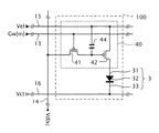
図2は、画素回路100の構成の一例を示す等価回路図である。図2では、第m行第k列の画素回路100を例示して説明する。
FIG. 2 is an equivalent circuit diagram showing an example of the configuration of the
画素回路100は、発光素子3と、発光素子3に供給する電流を出力する供給回路40と、を備える。
The
発光素子3は、画素電極31と、発光機能層32と、対向電極33とを備える。画素電極31は、発光機能層32に正孔を供給する陽極として機能する。対向電極33は、画素回路100の低電位側の電源電位である電位Vctに設定された給電線16に電気的に接続され、発光機能層32に電子を供給する陰極として機能する。そして、画素電極31から供給される正孔と、対向電極33から供給される電子とが発光機能層32で結合し、発光機能層32が白色に発光する。
なお、詳細は後述するが、Rを発光可能な画素回路100が有する発光素子3(以下、発光素子3Rと称する)には、赤色のカラーフィルター81Rが重ねて配置される。Bを発光可能な画素回路が有する発光素子3(以下、発光素子3Bと称する)には、青色のカラーフィルター81Bが重ねて配置される。そして、Gを発光可能な画素回路100が有する発光素子3(以下、発光素子3Gと称する)には、緑色のカラーフィルター81Gが重ねて配置される。このため、発光素子3R、3G、および、3Bにより、フルカラーの表示が可能となる。
The
Although details will be described later, a
供給回路40は、Pチャネル型のトランジスター41および42と、保持容量44と、を備える。なお、トランジスター41および42の一方または両方は、Nチャネル型のトランジスターであってもよい。また、本実施形態では、トランジスター41および42が、薄膜トランジスターの場合を例示して説明するが、トランジスター41および42は、MOSFET(metal-oxide-semiconductor field-effect transistor)等の電界効果トランジスターであってもよい。
The
トランジスター41は、ゲートが、第m行の走査線13に電気的に接続され、ソースまたはドレインの一方が、第k列のデータ線14に電気的に接続され、ソースまたはドレインの他方が、トランジスター42のゲートと、保持容量44が有する2つの電極のうち一方の電極と、に電気的に接続されている。
トランジスター42は、ゲートが、トランジスター41のソースまたはドレインの他方と、保持容量44の一方の電極と、に電気的に接続され、ソースまたはドレインの一方が、画素電極31に電気的に接続され、ソースまたはドレインの他方が、画素回路100の高電位側の電源電位である電位Velに設定された給電線15に電気的に接続されている。
保持容量44は、保持容量44が有する2つの電極のうち一方の電極が、トランジスター41のソースまたはドレインの他方と、トランジスター42のゲートと、に電気的に接続され、保持容量44が有する2つの電極のうち他方の電極が、給電線15に電気的に接続されている。保持容量44は、トランジスター42のゲートの電位を保持する保持容量として機能する。
The gate of the
The
In the
走査線駆動回路111が、走査信号Gw[m]を所定の選択電位に設定し、第m行の走査線13を選択すると、第m行第k列のサブ画素Px[m][k]に設けられたトランジスター41がオンする。そして、トランジスター41がオンすると、第k列のデータ線14から、トランジスター42のゲートに対して、データ信号Vd[k]が供給される。この場合、トランジスター42は、発光素子3に対して、ゲートに供給されたデータ信号Vd[k]の電位(正確には、ゲートおよびソース間の電位差)に応じた電流を供給する。つまり、トランジスター42は発光素子3へ電流を供給する駆動トランジスターである。発光素子3は、トランジスター42から供給される電流の大きさに応じた輝度、すなわち、データ信号Vd[k]の電位に応じた輝度で発光する。
その後、走査線駆動回路111が、第m行の走査線13の選択を解除して、トランジスター41がオフした場合、トランジスター42のゲートの電位は、保持容量44により保持される。このため、発光素子3は、トランジスター41がオフした後も、データ信号Vd[k]に応じた輝度で発光することができる。
When the scanning line drive circuit 111 sets the scanning signal Gw [m] to a predetermined selection potential and selects the
Thereafter, when the scanning line driving circuit 111 cancels the selection of the
なお、図2では図示省略するが、発光素子3が有する画素電極31と供給回路40とを電気的に接続する構成要素を、コンタクト7(図3参照)と称する。各サブ画素Pxは、発光素子3と、供給回路40と、コンタクト7が配置されるコンタクト領域Caを備える。コンタクト領域Caは、コンタクト7が配置可能な領域である。コンタクト7は、発光素子3が有する画素電極31と、供給回路40とを電気的に接続する。以下では、サブ画素PxRに設けられたコンタクト7を、コンタクト7Rと称し、サブ画素PxGに設けられたコンタクト7を、コンタクト7Gと称し、サブ画素PxBに設けられたコンタクト7を、コンタクト7Bと称する場合がある。また、コンタクト7Rを配置するコンタクト領域Caを、コンタクト領域CaRと称し、コンタクト7Gを配置するコンタクト領域Caを、コンタクト領域CaGと称し、コンタクト7Bを配置するコンタクト領域Caを、コンタクト領域CaBと称する場合がある。
Although not shown in FIG. 2, a component that electrically connects the
A.2.表示部の構成
以下、図3〜図6を参照しつつ、本実施形態に係る表示部12の構成の一例を説明する。
A. 2. Configuration of Display Unit Hereinafter, an example of the configuration of the
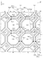
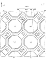
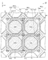
図3は、本実施形態に係る表示部12の一部を、電気光学装置1が光を射出する方向である+Z方向から平面視した場合の、表示部12の概略的な構成の一例を示す平面図である。ただし、図3に示す平面図は、図を見易くするために、カラーフィルター81を除いて表示してある。また、コンタクト領域CaR、およびCaGには、それぞれ2つのコンタクト7が配置されるが、図3に示す平面図は、図を見易くするために、2つのコンタクト7をまとめて、単に1つのコンタクト7として表示する。
FIG. 3 illustrates an example of a schematic configuration of the
具体的には、図3は、表示部12のうち、ある画素MPx1を形成するサブ画素PxR、サブ画素PxG、サブ画素PxB1、および、サブ画素PxB2を含む。サブ画素PxRは、Rを表示可能な画素回路100内の発光素子3Rを含む。サブ画素PxGは、Gを表示可能な画素回路100内の発光素子3Gを含む。サブ画素PxB1は、Bを表示可能な画素回路100内の発光素子3B1を含む。また、サブ画素PxB2は、Bを表示可能な画素回路100内の発光素子3B2を含む。そして、サブ画素PxB1およびサブ画素PxB2は、同一の画素回路100に含まれる供給回路40から電流が供給される。
Specifically, FIG. 3 includes a sub-pixel PxR, a sub-pixel PxG, a sub-pixel PxB1, and a sub-pixel PxB2 which form a certain pixel MPx1 in the
図3に示すように、+X方向に沿って、サブ画素PxB1、および、サブ画素PxGが配置される。同様に、+X方向に沿って、サブ画素PxR、および、サブ画素PxB2が配置される。また、+Y方向に沿って、サブ画素PxB1、および、サブ画素PxRが配置される。同様に、+Y方向に沿って、サブ画素PxG、および、サブ画素PxB2が配置される。サブ画素PxB1は、サブ画素PxB1から見てA方向に位置するサブ画素PxB2と、反射層52(図7参照)において接続する。本実施形態では、画素MPxが有する発光素子3R、3G、3B1、3B2のそれぞれにより、+Z方向に向けて光を射出する発光領域HaR、HaG、HaB1、HaB2が形成される場合を想定する。発光領域Haは、画素電極31(図7参照)の領域のうち画素分離層34(図7参照)によって開口されている領域である。
As shown in FIG. 3, the sub-pixel PxB1 and the sub-pixel PxG are arranged along the + X direction. Similarly, the sub-pixel PxR and the sub-pixel PxB2 are arranged along the + X direction. Further, the sub-pixel PxB1 and the sub-pixel PxR are disposed along the + Y direction. Similarly, the sub-pixel PxG and the sub-pixel PxB2 are arranged along the + Y direction. The sub-pixel PxB1 is connected to the sub-pixel PxB2 located in the A direction as viewed from the sub-pixel PxB1 in the reflective layer 52 (see FIG. 7). In the present embodiment, it is assumed that light emitting areas HaR, HaG, HaB1 and HaB2 for emitting light in the + Z direction are formed by the
+Z方向から平面視した場合の発光領域HaR、HaG、HaB1、およびHaB2の形状は、8角形である。発光領域Haの各辺のうち、発光領域Haの中心から見てC方向に位置する第1の辺と、発光領域Haの中心から見てA方向に位置する第5の辺とが平行である。また、発光領域Haの各辺のうち、発光領域Haの中心から見て−Y方向に位置する第2の辺と、発光領域Haの中心から見て+Y方向に位置する第6の辺とが平行である。また、発光領域Haの各辺のうち、発光領域Haの中心から見てD方向に位置する第3の辺と、発光領域Haの中心から見てB方向に位置する第7の辺とが平行である。また、発光領域Haの各辺のうち、発光領域Haの中心から見て+X方向に位置する第4の辺と、発光領域Haの中心から見て−X方向に位置する第8の辺とが平行である。 The shape of the light emitting regions HaR, HaG, HaB1, and HaB2 when viewed in plan from the + Z direction is octagonal. Among the sides of the light emitting area Ha, the first side located in the C direction as viewed from the center of the light emitting area Ha and the fifth side located in the A direction as viewed from the center of the light emitting area Ha are parallel . Further, among the sides of the light emitting area Ha, the second side located in the -Y direction as viewed from the center of the light emitting area Ha and the sixth side located in the + Y direction as viewed from the center of the light emitting area Ha It is parallel. Further, among the sides of the light emitting area Ha, the third side located in the D direction as viewed from the center of the light emitting area Ha and the seventh side located in the B direction as viewed from the center of the light emitting area Ha are parallel It is. Further, among the sides of the light emitting area Ha, the fourth side located in the + X direction as viewed from the center of the light emitting area Ha and the eighth side located in the −X direction as viewed from the center of the light emitting area Ha It is parallel.
また、サブ画素Pxが備えるコンタクト領域Caは、サブ画素Pxが備える発光領域Haから見て、A方向に位置する。具体的には、サブ画素PxRが備えるコンタクト領域CaRは、サブ画素PxRが備える発光領域HaRのA方向に位置する。同様に、サブ画素PxGが備えるコンタクト領域CaGは、サブ画素PxGが備える発光領域HaGのA方向に位置する。同様に、サブ画素PxB1が備えるコンタクト領域CaB1は、サブ画素PxB1が備える発光領域HaB1のA方向に位置する。同様に、サブ画素PxB2が備えるコンタクト領域CaB2は、サブ画素PxB2が備える発光領域HaB2のA方向に位置する。 Further, the contact region Ca included in the sub pixel Px is located in the A direction as viewed from the light emitting region Ha included in the sub pixel Px. Specifically, the contact region CaR included in the sub pixel PxR is located in the A direction of the light emitting region HaR included in the sub pixel PxR. Similarly, the contact region CaG included in the sub pixel PxG is located in the A direction of the light emitting region HaG included in the sub pixel PxG. Similarly, the contact region CaB1 included in the sub-pixel PxB1 is located in the direction A of the light-emitting region HaB1 included in the sub-pixel PxB1. Similarly, the contact region CaB2 included in the sub-pixel PxB2 is located in the A direction of the light-emitting region HaB2 included in the sub-pixel PxB2.
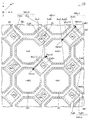
図4は、本実施形態に係る表示部12の一部を、+Z方向から平面視した場合の、表示部12の概略的な構成の一例を示す平面図である。ただし、図4に示す平面図は、図を見易くするために、カラーフィルター81を除いて表示してある。図4における斜め方向は、+X方向に対して45度で傾き、かつ+Y方向に対して−45度で傾いたA方向であるとする。
FIG. 4 is a plan view showing an example of a schematic configuration of the
コンタクト領域Caは、A方向に沿って並んでいる。コンタクト領域CaB1内には、コンタクト7B1が配置され、コンタクト領域CaB2内には、コンタクト7B2が配置される。コンタクト7B1、およびコンタクト7B2は、コンタクト電極71(図7参照)を介して、画素電極31と反射層52(図7参照)とを電気的に接続する。
一方、コンタクト領域CaRには、反射層52とコンタクト電極71とを電気的に接続する反射層−バリアメタルコンタクト7aRと、コンタクト電極71と画素電極31とを電気的に接続するバリアメタル−陽極コンタクト7bRとが配置される。同様に、コンタクト領域CaGには、反射層−バリアメタルコンタクト7aGと、バリアメタル−陽極コンタクト7bGとが配置される。ここで、コンタクト領域CaR、およびコンタクト領域CaGに、2つのコンタクト7がある理由について説明する。サブ画素PxRには、第1の距離調整層57(図15参照)および第2の距離調整層58(図15参照)が積層されており、また、サブ画素PxGには、第2の距離調整層58が積層されている。このように、距離調整層が存在するために、コンタクト領域CaR、およびコンタクト領域CaG内には、反射層−バリアメタルコンタクト7aを避けた別の場所に、バリアメタル−陽極コンタクト7bが形成される。
The contact regions Ca are aligned along the A direction. The contact 7B1 is disposed in the contact region CaB1, and the contact 7B2 is disposed in the contact region CaB2. The contacts 7B1 and 7B2 electrically connect the
On the other hand, in the contact region CaR, a reflective layer-barrier metal contact 7aR electrically connecting the
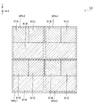
図5は、本実施形態に係る表示部12の一部を、+Z方向から平面視した場合の、表示部12の概略的な構成の一例を示す平面図である。図5に示す平面図は、図3および図4に示した平面図に、カラーフィルター81を加えた図である。さらに、図5に示す平面図は、図を見易くするために、コンタクト領域Caを除いて表示してある。
FIG. 5 is a plan view showing an example of a schematic configuration of the
カラーフィルター81Rは、発光素子3Rの+Z側において、+Z方向からの平面視においてサブ画素PxRと重なるように形成されている。同様に、カラーフィルター81Gは、発光素子3Gの+Z側において、+Z方向からの平面視においてサブ画素PxGと重なるように形成されている。カラーフィルター81B1は、発光素子3B1の+Z側において、+Z方向からの平面視においてサブ画素PxB1と重なるように形成されている。カラーフィルター81B2は、発光素子3B2の+Z側において、+Z方向からの平面視においてサブ画素PxB2と重なるように形成されている。図5に示すように、本実施形態において、+Z方向から平面視した場合のカラーフィルター81は、矩形形状である。また、図5に示すように、本実施形態では、カラーフィルター81同士は重ならないが、カラーフィルター81同士の一部が重なってもよい。また、X軸方向とY軸方向とのいずれかの方向について、カラーフィルター81の端部から、該当のカラーフィルター81に前述のいずれかの方向で隣り合う発光領域Haまでの距離は、同一となる。
The
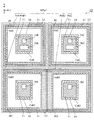
図6に、本実施形態に係る表示部12の一部を、+Z方向から平面視した場合の、表示部12の概略的な構成の一例を示す平面図を示す。図6に示す平面図は、画素MPx1〜MPx4のカラーフィルター81だけを表示してある。
FIG. 6 is a plan view showing an example of a schematic configuration of the
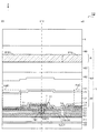
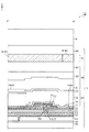
図7は、表示部12を、図5におけるE0−E’0−e0線で破断した部分断面図の一例であり、コンタクト7B1の断面を含む。
FIG. 7 is an example of a partial cross-sectional view in which the
図7に示すように、表示部12は、素子基板5と、保護基板9と、素子基板5および保護基板9の間に設けられた接着層90と、を備える。なお、本実施形態では、電気光学装置1が保護基板9側(+Z側)から光を射出するトップエミッション方式である場合を想定する。
As shown in FIG. 7, the
接着層90は、素子基板5および保護基板9を接着するための透明な樹脂層である。接着層90は、例えば、エポキシ樹脂といった透明な樹脂材料を用いて形成される。
保護基板9は、接着層90の+Z側に配置される透明な基板である。保護基板9は、カラーフィルター81といった、保護基板9より−Z側に配置される部材を保護する。保護基板9は、例えば、石英基板を用いて形成される。
The
The
素子基板5は、基板50と、基板50に形成された回路層49と、回路層49上に積層された層間絶縁層51と、反射層52と、増反射層53と、第1の絶縁層54と、第2の絶縁層55と、コンタクト電極71と、保護層72と、発光層30と、封止層60と、カラーフィルター層8と、を備える。詳細は後述するが、発光層30は、上述した発光素子3(3R、3G、3B)を含む。発光素子3は、+Z方向および−Z方向に対して光を射出する。また、カラーフィルター層8は、上述したカラーフィルター81R、カラーフィルター81G、およびカラーフィルター81Bを含む。
The
基板50には、基板50は、各種配線および各種回路を実装可能な基板であればよい。基板50は、例えば、シリコン基板、石英基板、または、ガラス基板等を採用することができる。基板50の+Z側には、回路層49が形成される。
回路層49は、走査線13やデータ線14等の各種配線と、駆動回路11および画素回路100等の各種回路とが形成されている。回路層49の+Z側には、層間絶縁層51が積層される。
The
In the
層間絶縁層51は、例えば酸化シリコン(SiO2)などの絶縁材料が用いられている。層間絶縁層51の+Z側には、反射層52が積層される。
反射層52は、発光層30の発光素子3から射出された光を+Z方向側に反射するための構成要素である。反射層52として、例えば、チタン(Ti)膜の上に、アルミニウム(Al)と銅(Cu)との合金(AlCu)膜が形成される。反射層52は、サブ画素Pxごとに個別に島状に形成された、反射性を有する導電層である。
The interlayer insulating
The
増反射層53は、反射層52による反射特性を高めるためのものであり、例えば光透過性を有する絶縁材料から形成される。増反射層53は、反射層52の面上を覆うように配置されている。増反射層53として、例えば、酸化シリコン膜が形成される。
The
第1の絶縁層54は、増反射層53の面上に設けられる。ここで、第1の絶縁層54は、反射層52に設けられた間隙52CTに沿って形成される。従って、第1の絶縁層54は、間隙52CTに対応した凹部54aを有している。埋め込み絶縁膜56は、凹部54aを埋めるように形成されている。第2の絶縁層55は、第1の絶縁層54の面上に設けられる。第1の絶縁層54および第2の絶縁層55として、例えば、窒化シリコン(SiN)膜が形成される。
The first insulating
コンタクト電極71は、反射層52および保護層72上に積層されており、間隙53CTに沿って形成されている。図7に示すように、コンタクト電極71が間隙53CTに沿うことにより、コンタクト7B1が形成される。コンタクト電極71には、例えば、タングステン(W)やチタン(Ti)、窒化チタン(TiN)などの導電材料を用いることができる。保護層72は、第2の絶縁層55上に積層される。保護層72には、酸化シリコンなどの絶縁材料が用いられている。
The
第1の距離調整層57および第2の距離調整層58は、サブ画素PxR、PxG、PxBごとに、発光層30の発光素子3と反射層52との間の光学的距離を調整するための、絶縁性の透明層である。本実施形態では、第1の距離調整層57および第2の距離調整層58として、酸化シリコン膜が形成される。サブ画素PxBについては、第1の距離調整層57および第2の距離調整層58が積層されない。また、サブ画素PxGには、第2の距離調整層58だけが積層され、第1の距離調整層57は積層されない。従って、第1の距離調整層57は、図7では不図示である。
The first
発光層30は、画素電極31と、画素分離層34と、画素電極31および画素分離層34を覆うように積層された発光機能層32と、発光機能層32上に積層された対向電極33と、を有する。
The
画素電極31は、サブ画素Pxごとに個別に島状に形成された、導電性を有する透明層である。画素電極31は、第2の絶縁層55、第1の距離調整層57および第2の距離調整層58上に積層される。画素電極31は、導電性の透明材料、例えば、ITO(Indium Tin Oxide)を用いて形成される。
対向電極33は、複数のサブ画素Pxに跨るように配置された、光透過性と光反射性とを有する導電性の構成要素である。対向電極33は、例えば、MgとAgとの合金等を用いて形成される。
画素分離層34は、各画素電極31の周縁部を覆うように配置された、絶縁性の構成要素である。画素分離層34は、第2の距離調整層58、第2の絶縁層55および画素電極31上に積層される。画素分離層34は、絶縁性の材料、例えば、酸化シリコン等を用いて形成される。
発光機能層32は、正孔注入層、正孔輸送層、有機発光層、および電子輸送層を備え、複数のサブ画素Pxに跨るように配置されている。
The
The
The
The light emitting
上述のとおり、発光機能層32は、画素電極31のうち画素分離層34により覆われていない部分から正孔が供給され、白色に発光する。
また、平面視した場合に、画素分離層34は、表示部12の有する複数の画素Pxを互いに区画するように配置される。なお、発光素子3から射出される白色の光とは、赤色の光、緑色の光、および青色の光を含む光である。
なお、本実施形態では、+Z方向からの平面視において、発光領域Haと、コンタクト領域Caとを含む領域に含まれる構造物を、サブ画素Pxと看做すこととする。
As described above, the light emitting
Further, when viewed in a plan view, the
In the present embodiment, the structure included in the area including the light emitting area Ha and the contact area Ca is regarded as a sub-pixel Px in a plan view from the + Z direction.
本実施形態では、反射層52と対向電極33とにより、光共振構造が形成されるように、第1の距離調整層57および第2の距離調整層58の膜厚が調整される。そして、発光機能層32から射出された光は、反射層52と対向電極33との間で繰り返し反射され、反射層52と対向電極33との間の光学的距離に対応する波長の光の強度が強められ、当該強められた光が、対向電極33〜保護基板9を介して+Z側に射出される。
本実施形態では、一例として、サブ画素PxRにおいては、610nmの波長の光の強度が強められ、サブ画素PxGにおいては、540nmの波長の光の強度が強められ、サブ画素PxBにおいては、470nmの波長の光の強度が強められるように、サブ画素Pxごとに第1の距離調整層57および第2の距離調整層58の膜厚が設定される。このため、本実施形態において、サブ画素PxRからは、610nmの波長の光の輝度が最大となる赤色光が射出され、サブ画素PxGからは、540nmの波長の光の輝度が最大となる緑色光が射出され、サブ画素PxBからは、470nmの波長の光の輝度が最大となる青色光が射出されることになる。
In the present embodiment, the film thicknesses of the first
In the present embodiment, as an example, in the sub-pixel PxR, the intensity of light of a wavelength of 610 nm is enhanced, in the sub-pixel PxG, the intensity of light of a wavelength of 540 nm is enhanced, and in the sub-pixel PxB, 470 nm The film thicknesses of the first
封止層60は、対向電極33上に積層された下側封止層61と、下側封止層61上に積層された平坦化層62と、平坦化層62上に積層された上側封止層63と、を備える。
下側封止層61および上側封止層63は、複数のサブ画素Pxに跨るように配置された、絶縁性を有する透明層である。下側封止層61および上側封止層63は、水分や酸素等の発光層30への侵入を抑止するための構成要素である。下側封止層61および上側封止層63として、例えば、酸化窒化シリコン(SiON)膜が形成される。
平坦化層62は、複数のサブ画素Pxに跨るように配置された透明層であり、平坦な上面(+Z側の面)を提供するための構成要素である。平坦化層62は、例えば、エポキシ樹脂といった無機材料を用いて形成される。
The
The
The
カラーフィルター層8は、カラーフィルター81R、81G、81B1、および81B2を含む。カラーフィルター81R、81G、81B1、および81B2は、上側封止層63上に形成される。
カラーフィルター81R、81G、81B1、および81B2は、例えば赤、緑、青の異なる色の光を透過させるような顔料を含む感光性樹脂を塗布してパターン加工を行うことにより形成する。
The
The
図8は、表示部12を、図5におけるE1−e1線で破断した部分断面図の一例であり、コンタクト7B1の断面を含む。図8では、図7で説明した箇所については説明を省略する。
FIG. 8 is an example of a partial cross-sectional view in which the
図7では、は間隙52CTが現れていたが、サブ画素PxB1、およびPxB2が反射層52において接続するため、図5におけるE1−e1線で破断した部分においては間隙52CTが現れない。従って、間隙52CTは、図8では不図示である。また、サブ画素PxBについては、第1の距離調整層57および第2の距離調整層58が積層されないため、図8では不図示である。
In FIG. 7, the gap 52CT appears, but since the sub-pixels PxB1 and PxB2 are connected in the
A.3.本実施形態の効果
図3に示すように、+Z方向からの平面視において、コンタクト領域Caは、発光領域Haを区分けする境界線の交点と重なる。境界線は、発光領域Haを均等に区分けする線である。図3には、X軸方向の境界線HL1、およびHL2、ならびに、Y軸方向の境界線VL1、およびVL2を示す。図3に示すように、画素MPx1に含まれるコンタクト領域CaB1は、境界線VL1、およびHL1の交点P11と重なる。同様に、画素MPx1に含まれるコンタクト領域CaGは、境界線VL2、およびHL1の交点P21と重なる。同様に、画素MPx1に含まれるコンタクト領域CaRは、境界線VL1、およびHL2の交点P12と重なる。同様に、画素MPx1に含まれるコンタクト領域CaB2は、境界線VL2、およびHL2の交点P22と重なる。例えば、交点P11は、発光領域HaR、HaG、HaB1、HaB2の中心から離れた位置にあるため、発光領域HaR、HaG、HaB1、HaB2が小さくなることを抑制することができる。さらに、コンタクト領域Caを、発光領域Haを区分けする境界線の交点と重なるように配置することにより、隣接する他のサブ画素Pxの一部のエリアを使ってコンタクト領域Caを配置することができる。そして、あるサブ画素Pxの一部のエリアおよび隣接する他のサブ画素Pxの一部のエリアを使ってあるサブ画素Pxのコンタクト領域Caを配置することは、境界線を跨ってコンタクト領域Caを配置することになる。以上により、コンタクト領域Caをサブ画素間で均等な間隔で配置することが可能になり、発光領域の間隔も一定となる。本実施形態では、図3に示すように、発光領域Haは、四角形の各頂点を削った8角形の形状となる。そして、図3に示すように、削った部分にコンタクト領域Caが配置されている。図3に示すように、コンタクト領域Caをサブ画素Px間で均等な間隔で配置することが可能になり、発光領域Haの間隔も一定となる。発光領域Haの間隔が一定となることにより、視野角による色変化のばらつきを抑えることが可能になる。このように、発光領域Haが小さくなることを抑制しつつ、視野角による色変化のばらつきを抑えることが可能になる。視野角による色変化のばらつきを抑えることにより、表示画像の品質の低下を抑制することが可能になる。
A. 3. Effects of the Present Embodiment As shown in FIG. 3, in a plan view from the + Z direction, the contact region Ca overlaps the intersection of the boundaries dividing the light emitting region Ha. The boundary line is a line which equally divides the light emitting area Ha. FIG. 3 shows the boundaries HL1 and HL2 in the X-axis direction and the boundaries VL1 and VL2 in the Y-axis direction. As shown in FIG. 3, the contact region CaB1 included in the pixel MPx1 overlaps the intersection point P11 of the boundary lines VL1 and HL1. Similarly, the contact region CaG included in the pixel MPx1 overlaps the intersection point P21 of the boundary lines VL2 and HL1. Similarly, the contact region CaR included in the pixel MPx1 overlaps the intersection point P12 of the boundary lines VL1 and HL2. Similarly, the contact region CaB2 included in the pixel MPx1 overlaps the intersection point P22 of the boundary lines VL2 and HL2. For example, since the intersection point P11 is located at a position distant from the center of the light emitting regions HaR, HaG, HaB1, and HaB2, the light emitting regions HaR, HaG, HaB1, and HaB2 can be suppressed from being reduced. Furthermore, by arranging the contact region Ca so as to overlap the intersection of the boundaries dividing the light emitting region Ha, it is possible to arrange the contact region Ca using a part of the area of another adjacent sub-pixel Px. . Then, arranging the contact region Ca of a certain sub-pixel Px using a partial area of a certain sub-pixel Px and a partial area of another adjacent sub-pixel Px makes the contact region Ca straddle the border line. It will be arranged. As described above, it is possible to arrange the contact regions Ca at equal intervals between the sub-pixels, and the intervals of the light emitting regions also become constant. In the present embodiment, as shown in FIG. 3, the light emitting area Ha has an octagonal shape in which each vertex of the quadrangle is cut. And as shown in FIG. 3, contact area | region Ca is arrange | positioned in the shaved part. As shown in FIG. 3, the contact regions Ca can be arranged at equal intervals between the sub-pixels Px, and the distance between the light emitting regions Ha also becomes constant. When the distance between the light emitting regions Ha is constant, it is possible to suppress the variation in color change due to the viewing angle. As described above, it is possible to suppress the variation of the color change due to the viewing angle while suppressing the reduction of the light emitting region Ha. By suppressing the variation of the color change due to the viewing angle, it is possible to suppress the deterioration of the quality of the display image.
ここで、視野角とは、サブ画素Pxが備える発光領域Haから射出された光であって、前述したサブ画素Pxが備えるカラーフィルター81および保護基板9を透過する光の進行方向と、Z軸方向とのなす角度の最大値である。以下、+Z方向からの平面視において前述した光の方向を、前述の方向の視野角と称する場合がある。例えば、前述した光がXZ平面内に含まれる場合、+Z方向からの平面視では、前述した光の方向は、X軸方向となるため、「X軸方向の視野角」と称する場合がある。同様に、前述した光がYZ平面内に含まれる場合、+Z方向からの平面視では、前述した光の方向は、Y軸方向となるため、「Y軸方向の視野角」と称する場合がある。
Here, the viewing angle is the light emitted from the light emitting area Ha of the sub pixel Px, and the traveling direction of the light transmitted through the color filter 81 and the
X軸方向の視野角について、図3に示したように、画素MPx1における発光領域HaB1と発光領域HaGとの間の距離dx12は、画素MPx1の発光領域HaGと画素MPx1に対して+X方向に並ぶ画素MPx2における発光領域HaB1との間の距離dx34と略等しい。ここで、距離dx12が距離dx34と略等しいについて、例えば、距離dx12と距離dx34との差分が所定の閾値以下となれば、距離dx12が距離dx34と略等しいとする。所定の閾値は、例えば、発光領域Haの幅の10%である。距離dx12は、図3に示すように、画素MPx1における発光領域HaB1の+X方向にある頂点Apx1と、画素MPx1における発光領域HaGの−X方向にある頂点Apx2との最短距離である。同様に、距離dx34は、画素MPx1における発光領域HaGの+X方向にある頂点Apx3と、画素MPx2における発光領域HaB1の−X方向にある頂点Apx4との最短距離である。なお、発光領域Ha同士の距離は、発光領域Haの頂点からの最短距離に限らず、発光領域Haの中心同士の最短距離でもよい。
同様に、画素MPx1における発光領域HaRと発光領域HaB2との間の距離dx56は、画素MPx1の発光領域HaB2と画素MPx2における発光領域HaRとの間の距離dx78と略等しい。換言すれば、X軸方向に沿った発光領域Ha同士の距離が一定である。
距離dx12が距離dx34と略等しいことにより、画素MPx1における発光素子3Gのカラーフィルター81Gの−X方向の端部および頂点Apx1を結ぶ直線とX軸方向とのなす角度が、画素MPx2における発光素子3B1のカラーフィルター81Bの−X方向の端部および頂点Apx3を結ぶ直線とX軸方向とのなす角度と略等しくなる。距離dx56と距離dx78についても、距離dx12と距離dx34と同様の関係が成り立つ。従って、視野角が前述した2つの角度に略等しい場合、画素MPx1における発光領域HaB1から射出される光の色変化と、画素MPx1における発光領域HaGから射出される光の色変化とが共に発生することになる。このように、X軸方向において隣り合う発光領域Haの色変化が発生する角度が略等しくなるため、X軸方向に沿って配置された発光領域Ha間の距離のばらつきによって発生する、X軸方向の視野角による色変化のばらつきを抑えることが可能になる。
For the viewing angle in the X-axis direction, as shown in FIG. 3, the distance dx12 between the light emitting area HaB1 and the light emitting area HaG in the pixel MPx1 is aligned in the + X direction with respect to the light emitting area HaG of the pixel MPx1 and the pixel MPx1 It is approximately equal to the distance dx34 between the pixel MPx2 and the light emitting area HaB1. Here, when the distance dx12 is substantially equal to the distance dx34, for example, it is assumed that the distance dx12 is substantially equal to the distance dx34 if the difference between the distance dx12 and the distance dx34 is less than or equal to a predetermined threshold. The predetermined threshold is, for example, 10% of the width of the light emitting area Ha. The distance dx12 is the shortest distance between the vertex Apx1 in the + X direction of the light emitting area HaB1 in the pixel MPx1 and the vertex Apx2 in the −X direction of the light emitting area HaG in the pixel MPx1, as shown in FIG. Similarly, the distance dx34 is the shortest distance between the vertex Apx3 in the + X direction of the light emitting region HaG in the pixel MPx1 and the vertex Apx4 in the −X direction of the light emitting region HaB1 in the pixel MPx2. The distance between the light emitting regions Ha is not limited to the shortest distance from the vertex of the light emitting region Ha, but may be the shortest distance between the centers of the light emitting regions Ha.
Similarly, the distance dx56 between the light emitting area HaR and the light emitting area HaB2 in the pixel MPx1 is substantially equal to the distance dx78 between the light emitting area HaB2 in the pixel MPx1 and the light emitting area HaR in the pixel MPx2. In other words, the distance between the light emitting regions Ha along the X-axis direction is constant.
Since the distance dx12 is substantially equal to the distance dx34, the light emitting element 3B1 in the pixel MPx2 is formed by the straight line connecting the end of the
Y軸方向の視野角について、図3に示したように、画素MPx1における発光領域HaB1と発光領域HaRとの間の距離dy12は、画素MPx1の発光領域HaRと画素MPx1に対して+Y方向に並ぶ画素MPx3における発光領域HaB1との間の距離dy34と略等しい。ここで、距離dy12が距離dy34と略等しいについて、例えば、距離dy12と距離dy34との差分が所定の閾値以下となれば、距離dy12が距離dy34と略等しいとする。所定の閾値は、例えば、は発光領域Haの高さの10%である。距離dy12は、図3に示すように、画素MPx1における発光領域HaB1の+Y方向にある頂点Apy1と、画素MPx1における発光領域HaRの−Y方向にある頂点Apy2との最短距離である。同様に、距離dy34は、画素MPx1における発光領域HaRの+Y方向にある頂点Apy3と、画素MPx3における発光領域HaB1の−Y方向にある頂点Apy4との最短距離である。
同様に、画素MPx1における発光領域HaGと発光領域HaB2との間の距離dy56は、画素MPx1の発光領域HaB2と画素MPx3における発光領域HaGとの間の距離dy78と略等しい。換言すれば、Y軸方向に沿った発光領域Ha同士の距離が一定である。
距離dy12が距離dy34と略等しいこと、および、距離dy56が距離dy78と略等しいことにより、X軸方向と同様に、Y軸方向に沿って配置された発光領域Ha間の距離のばらつきによって発生する、Y軸方向の視野角による色変化のばらつきを抑えることが可能になる。
Regarding the viewing angle in the Y-axis direction, as shown in FIG. 3, the distance dy12 between the light emitting area HaB1 and the light emitting area HaR in the pixel MPx1 is aligned in the + Y direction with respect to the light emitting area HaR of the pixel MPx1 and the pixel MPx1. It is approximately equal to the distance dy34 between the pixel MPx3 and the light emitting area HaB1. Here, when the distance dy12 is substantially equal to the distance dy34, for example, it is assumed that the distance dy12 is substantially equal to the distance dy34 if the difference between the distance dy12 and the distance dy34 is less than or equal to a predetermined threshold. The predetermined threshold is, for example, 10% of the height of the light emitting area Ha. The distance dy12 is the shortest distance between the vertex Apy1 in the + Y direction of the light emitting area HaB1 in the pixel MPx1 and the vertex Apy2 in the −Y direction of the light emitting area HaR in the pixel MPx1, as shown in FIG. Similarly, the distance dy34 is the shortest distance between the vertex Apy3 in the + Y direction of the light emitting region HaR in the pixel MPx1 and the vertex Apy4 in the −Y direction of the light emitting region HaB1 in the pixel MPx3.
Similarly, the distance dy56 between the light emitting area HaG and the light emitting area HaB2 in the pixel MPx1 is substantially equal to the distance dy78 between the light emitting area HaB2 in the pixel MPx1 and the light emitting area HaG in the pixel MPx3. In other words, the distance between the light emitting regions Ha along the Y-axis direction is constant.
Similar to the X-axis direction, the distance dy12 is approximately equal to the distance dy34, and the distance dy56 is approximately equal to the distance dy78. This is caused by the variation in the distance between the light emitting areas Ha arranged along the Y-axis direction. It is possible to suppress the variation in color change due to the viewing angle in the Y-axis direction.
また、X軸方向の視野角について、図6に示すように、あるサブ画素Pxの色と、前述のあるサブ画素に対して+X方向に沿って配置されたサブ画素の色との関係は、前述のあるサブ画素の色に応じて一意に定まる。具体的には、画素MPx1〜MPx4のそれぞれのサブ画素PxRと+X方向において隣り合うカラーフィルター81は、カラーフィルター81Bとなる。同様に、画素MPx1〜MPx4のそれぞれのサブ画素PxGと+X方向において隣り合うカラーフィルター81は、カラーフィルター81Bとなる。画素MPx1〜MPx4のそれぞれのサブ画素PxBと+X方向において隣り合うカラーフィルター81は、カラーフィルター81R、または81Gとなる。そして、カラーフィルター81Rが隣り合う割合と、カラーフィルター81Gが隣り合う割合とは同一である。従って、+X方向において、ある視野角によって色変化が発生した際に、同一の色のサブ画素Pxでは、一意に定まった色変化が発生するため、+X方向に位置するカラーフィルター81の色のばらつきによって発生する、視野角による色変化のばらつきを抑えることができる。−X方向についても+X方向と同様である。
Further, regarding the viewing angle in the X-axis direction, as shown in FIG. 6, the relationship between the color of a certain sub-pixel Px and the color of the sub-pixel arranged along the + X direction with respect to the certain sub-pixel is Uniquely determined according to the color of a certain sub-pixel described above. Specifically, the color filter 81 adjacent to each sub-pixel PxR of the pixels MPx1 to MPx4 in the + X direction is a
また、Y軸方向の視野角に応じた色変化に関して、図6に示すように、あるサブ画素Pxの色と、前述のあるサブ画素に対して+Y方向に沿って配置されたサブ画素の色との関係は、前述のあるサブ画素の色に応じて一意に定まる。具体的には、画素MPx1〜MPx4のそれぞれのサブ画素PxRと+Y方向において隣り合うカラーフィルター81は、カラーフィルター81Bとなる。同様に、画素MPx1〜MPx4のそれぞれのサブ画素PxGと+Y方向において隣り合うカラーフィルター81は、カラーフィルター81Bとなる。画素MPx1〜MPx4のそれぞれのサブ画素PxBと+Y方向において隣り合うカラーフィルター81は、カラーフィルター81R、または81Gとなる。そして、カラーフィルター81Rが隣り合う割合と、カラーフィルター81Gが隣り合う割合とは同一である。従って、+Y方向において、ある視野角によって色変化が発生した際に、同一の色のサブ画素Pxでは、一意に定まった色変化が発生するため、+Y方向に位置するカラーフィルター81の色のばらつきによって発生する、視野角による色変化のばらつきを抑えることができる。−Y方向についても+Y方向と同様である。
In addition, regarding color change according to the viewing angle in the Y-axis direction, as shown in FIG. 6, the color of a certain sub-pixel Px and the color of a sub-pixel arranged along the + Y direction with respect to the certain sub-pixel The relationship with is uniquely determined in accordance with the color of a certain sub-pixel described above. Specifically, the color filter 81 adjacent in the + Y direction to the sub-pixels PxR of the pixels MPx1 to MPx4 is the
さらに、X軸方向の視野角による色変化およびY軸方向の視野角による色変化の関係に関して、サブ画素PxR、およびPxGのX軸方向、およびY軸方向において隣り合うカラーフィルター81が、カラーフィルター81Bとなる。また、サブ画素PxBのX軸方向、およびY軸方向において隣り合うカラーフィルター81が、カラーフィルター81R、または81Gとなる。このように、本実施形態では、X軸方向において隣り合う色の配置と、Y軸方向において隣り合う色の配置とが同一となるため、X軸方向の視野角による色変化と、Y軸方向の視野角による色変化とを同一にすることが可能になる。
Furthermore, with regard to the relationship between the color change due to the viewing angle in the X-axis direction and the color change due to the viewing angle in the Y-axis direction, the color filters 81 adjacent to each other in the X-axis direction of the sub-pixels PxR and PxG and in the Y-axis direction It will be 81B. Further, the color filters 81 adjacent in the X-axis direction and the Y-axis direction of the sub-pixel PxB become the
同様に、A方向、B方向、C方向、およびD方向による色変化に関しても、あるサブ画素Pxの色と、前述のあるサブ画素に対して+Y方向に沿って配置されたサブ画素の色との関係は、前述のあるサブ画素の色に応じて一意に定まる。従って、発光領域Haに、A方向、B方向、C方向、およびD方向のいずれにおいて隣り合うカラーフィルター81に関係する色変化のばらつきを抑えることができる。 Similarly, with regard to color change due to A direction, B direction, C direction, and D direction, the color of a certain sub-pixel Px and the color of a sub-pixel arranged along the + Y direction with respect to the certain sub-pixel The relationship is uniquely determined in accordance with the color of a certain sub-pixel described above. Therefore, it is possible to suppress the variation in color change related to the color filter 81 adjacent in any of the A direction, the B direction, the C direction, and the D direction in the light emitting region Ha.
また、図4に示すように、コンタクト領域Caは、+X方向に対して45度で傾き、+Y方向に対して−45度で傾くA方向に沿って並べられる。さらに、コンタクト領域CaR、およびCaGには、2つのコンタクト7を配置することにより、2つのコンタクト7を1箇所に集中させることになるため、2つのコンタクト7間の距離が短くなり、容易に配線を行うことが可能になる。また、2つのコンタクト7を1箇所に集中させることにより、コンタクト領域Caを狭くして、発光領域Haをより広く確保することが可能になる。
Further, as shown in FIG. 4, the contact regions Ca are arranged along the A direction which is inclined at 45 degrees with respect to the + X direction and inclined at -45 degrees with respect to the + Y direction. Furthermore, since the two
また、A方向の視野角について、図4に示すように、サブ画素Pxの発光領域Haと、前述のサブ画素Pxに対してA方向に沿って配置されたサブ画素Pxの発光領域Haとの間の距離が一定である。例えば、画素MPx1におけるサブ画素PxB1に対して、A方向に沿って画素MPx1におけるサブ画素PxB2が配置されている。また、画素MPx1におけるサブ画素PxB2に対して、A方向に沿って画素MPx4におけるサブ画素PxB1が配置されている。画素MPx4は、画素MPx1に対してA方向に並んで配置された画素である。
そして、距離が一定について、画素MPx1における発光領域HaB1と画素MPx1における発光領域HaB2との間の距離dxy12は、画素MPx1における発光領域HaB2と画素MPx4における発光領域HaB1との間の距離dxy34と略等しい。距離dx12は、図4に示すように、画素MPx1における発光領域HaB1のA方向にある頂点Apxy1と、画素MPx1における発光領域HaB2のC方向にある頂点Apxy2との最短距離である。同様に、距離dx34は、図4に示すように、画素MPx1における発光領域HaB2のA方向にある頂点Apxy3と、画素MPx4における発光領域HaB1のC方向にある頂点Apxy4との最短距離である。
距離dxy12が距離dxy34と略等しいことにより、X軸方向およびY軸方向と同様に、A方向、およびC方向に沿って配置された発光領域Ha間の距離のばらつきによって発生する、視野角による色変化のばらつきを抑えることが可能になる。
In addition, for the viewing angle in the A direction, as shown in FIG. 4, the light emitting area Ha of the sub pixel Px and the light emitting area Ha of the sub pixel Px disposed along the A direction with respect to the sub pixel Px described above. The distance between them is constant. For example, the sub-pixel PxB2 in the pixel MPx1 is disposed along the A direction with respect to the sub-pixel PxB1 in the pixel MPx1. Further, the sub-pixel PxB1 in the pixel MPx4 is disposed along the A direction with respect to the sub-pixel PxB2 in the pixel MPx1. The pixel MPx4 is a pixel arranged in the A direction with respect to the pixel MPx1.
Then, for a fixed distance, the distance dxy12 between the light emitting area HaB1 in the pixel MPx1 and the light emitting area HaB2 in the pixel MPx1 is approximately equal to the distance dxy34 between the light emitting area HaB2 in the pixel MPx1 and the light emitting area HaB1 in the pixel MPx4. . The distance dx12 is the shortest distance between the vertex Apxy1 in the A direction of the light emitting area HaB1 in the pixel MPx1 and the vertex Apxy2 in the C direction of the light emitting area HaB2 in the pixel MPx1, as shown in FIG. Similarly, as shown in FIG. 4, the distance dx34 is the shortest distance between the vertex Apxy3 in the A direction of the light emitting region HaB2 in the pixel MPx1 and the vertex Apxy4 in the C direction of the light emitting region HaB1 in the pixel MPx4.
Since the distance dxy12 is substantially equal to the distance dxy34, the color according to the viewing angle is generated due to the variation in the distance between the light emitting areas Ha disposed along the A direction and the C direction as in the X axis direction and the Y axis direction. It becomes possible to suppress the variation of change.
なお、本実施形態において、+X方向は「第1の方向」の一例であり、+Y方向は「第2の方向」の一例である。また、サブ画素PxB1は、「第1のサブ画素」の一例であり、サブ画素PxGは、「第2のサブ画素」の一例である。また、サブ画素PxRは、「第4のサブ画素」の一例であり、サブ画素PxB2は、「第3のサブ画素」の一例である。 In the present embodiment, the + X direction is an example of the “first direction”, and the + Y direction is an example of the “second direction”. Further, the sub-pixel PxB1 is an example of the “first sub-pixel”, and the sub-pixel PxG is an example of the “second sub-pixel”. The sub-pixel PxR is an example of the “fourth sub-pixel”, and the sub-pixel PxB2 is an example of the “third sub-pixel”.
なお、本実施形態において、45度は、「第1の角度」の例であり、−45度は、「第2の角度」の例である。また、A方向は、「第3の方向」の例である。また、コンタクト電極は、「中間電極」の例である。また、反射層52は、「反射電極」の例である。また、反射層−バリアメタルコンタクト7aは、「第1のコンタクト」の例である。また、バリアメタル−陽極コンタクト7bは、「第2のコンタクト」の例である。
In the present embodiment, 45 degrees is an example of the “first angle”, and −45 degrees is an example of the “second angle”. Also, the A direction is an example of the “third direction”. The contact electrode is an example of the “intermediate electrode”. The
B.変形例
以上の各形態は多様に変形され得る。具体的な変形の態様を以下に例示する。以下の例示から任意に選択された2以上の態様は、相互に矛盾しない範囲内で適宜に併合され得る。なお、以下に例示する変形例において作用や機能が実施形態と同等である要素については、以上の説明で参照した符号を流用して各々の詳細な説明を適宜に省略する。
B. Modified Embodiments The above embodiments can be variously modified. The aspect of a specific deformation | transformation is illustrated below. Two or more aspects arbitrarily selected from the following exemplifications may be combined as appropriate within the range not mutually contradictory. In addition, about the element in which an effect | action or a function is equivalent to embodiment in the modification illustrated below, the code | symbol referred by the above description is diverted and detailed description of each is abbreviate | omitted suitably.
B.1.第1の変形例
図9に、第1の変形例における表示部12の一部を、+Z方向から平面視した場合の、表示部12の概略的な構成の一例を示す平面図を示す。ただし、図9に示す平面図は、図を見易くするために、カラーフィルター81、およびコンタクト領域Caを除いて表示してある。なお、第1の変形例では、+Z方向からの平面視において、発光領域Haと、コンタクト領域Caとを含む領域に含まれる構造物を、サブ画素Pxと看做すこととする。
B. 1. First Modified Example FIG. 9 is a plan view showing an example of a schematic configuration of the
本実施形態では、サブ画素PxB1およびPxB2は、反射層52において接続している。一方、第1の変形例では、サブ画素PxB1およびPxB2が、接続しておらず、分離している。第1の変形例におけるサブ画素PxR、PxG、PxB1、およびPxB2を、3画素回路を用いて駆動させるには、分離した一方のサブ画素PxBを、回路層49内において、他方のサブ画素PxBの画素回路100に接続する必要がある。
In the present embodiment, the sub-pixels PxB1 and PxB2 are connected by the
図10に、第1の変形例における表示部12の一部を、+Z方向から平面視した場合の、表示部12の概略的な構成の一例を示す平面図を示す。図10に示す平面図は、図9に示した平面図に、カラーフィルター81を加えた図である。ただし、図10に示す平面図は、図を見易くするために、コンタクト領域Caを除いて表示してある。
FIG. 10 is a plan view showing an example of a schematic configuration of the
図10に示すように、第1の変形例におけるカラーフィルター81の配置位置は、本実施形態におけるカラーフィルター81の配置位置と同一である。従って、X軸方向の視野角による色変化の特性、および、Y軸方向の視野角による色変化の特性は、本実施形態の特性と同一となる。 As shown in FIG. 10, the arrangement position of the color filter 81 in the first modification is the same as the arrangement position of the color filter 81 in the present embodiment. Therefore, the characteristics of the color change due to the viewing angle in the X axis direction and the characteristics of the color change due to the viewing angle in the Y axis direction are the same as the characteristics of the present embodiment.
B.2.第2の変形例
図11に、第2の変形例における表示部12の一部を、+Z方向から平面視した場合の、表示部12の概略的な構成の一例を示す平面図を示す。ただし、図11に示す平面図は、図を見易くするために、カラーフィルター81、およびコンタクト領域Caを除いて表示してある。なお、第2の変形例では、+Z方向からの平面視において、発光領域Haと、コンタクト領域Caとを含む領域に含まれる構造物を、サブ画素Pxと看做すこととする。
B. 2. Second Modified Example FIG. 11 is a plan view showing an example of a schematic configuration of the
第2の変形例では、+X方向に沿って、サブ画素PxB1、および、サブ画素PxB2が配置される。同様に、+X方向に沿って、サブ画素PxR、および、サブ画素PxGが配置される。また、+Y方向に沿って、サブ画素PxB1、および、サブ画素PxRが配置される。同様に、+Y方向に沿って、サブ画素PxB2、および、サブ画素PxGが配置される。サブ画素PxB1は、サブ画素PxB1から見て+X方向に位置するサブ画素PxB2と、反射層52において接続する。このように、第2の変形例におけるサブ画素Pxの配置は、本実施形態におけるサブ画素Pxの配置から、サブ画素PxB2とサブ画素PxGを入れ替えた位置となる。
In the second modified example, the sub-pixel PxB1 and the sub-pixel PxB2 are disposed along the + X direction. Similarly, the sub-pixel PxR and the sub-pixel PxG are arranged along the + X direction. Further, the sub-pixel PxB1 and the sub-pixel PxR are disposed along the + Y direction. Similarly, the sub-pixel PxB2 and the sub-pixel PxG are arranged along the + Y direction. The sub-pixel PxB1 is connected to the sub-pixel PxB2 positioned in the + X direction as viewed from the sub-pixel PxB1 in the
なお、第2の変形例において、サブ画素PxB1は、「第1のサブ画素」の一例であり、サブ画素PxB2は、「第2のサブ画素」の一例である。また、サブ画素PxRは、「第4のサブ画素」の一例であり、サブ画素PxGは、「第3のサブ画素」の一例である。 In the second modification, the sub-pixel PxB1 is an example of the “first sub-pixel”, and the sub-pixel PxB2 is an example of the “second sub-pixel”. The sub-pixel PxR is an example of the “fourth sub-pixel”, and the sub-pixel PxG is an example of the “third sub-pixel”.
図12に、第2の変形例における表示部12の一部を、+Z方向から平面視した場合の、表示部12の概略的な構成の一例を示す平面図を示す。図12に示す平面図は、図11に示した平面図に、カラーフィルター81を加えた図である。ただし、図12に示す平面図は、図を見易くするために、コンタクト領域Caを除いて表示してある。
FIG. 12 is a plan view showing an example of a schematic configuration of the
カラーフィルター81Rは、発光領域HaRの+Z側において、+Z方向からの平面視においてサブ画素PxRと重なるように形成されている。同様に、カラーフィルター81Gは、発光領域HaGの+Z側において、+Z方向からの平面視においてサブ画素PxGと重なるように形成されている。カラーフィルター81Bは、発光領域HaB1、およびHaB2の+Z側において、+Z方向からの平面視においてサブ画素PxB1、およびPxB2と重なるように形成されている。カラーフィルター81Bは、X軸方向に沿って配置された各サブ画素PxBで共通のカラーフィルターとなる。
The
図13に、第2の変形例に係る表示部12の一部を、+Z方向から平面視した場合の、表示部12の概略的な構成の一例を示す平面図を示す。図13に示す平面図は、第2の変形例に係る画素MPx1〜MPx4のカラーフィルター81だけを表示してある。
FIG. 13 is a plan view showing an example of a schematic configuration of the
X軸方向の視野角に応じた色変化に関して、第2の変形例においても、あるサブ画素Pxの色と、前述のあるサブ画素に対してX軸方向に沿って配置されたサブ画素の色との関係は、前述のあるサブ画素の色に応じて一意に定まる。具体的には、画素MPx1〜MPx4のそれぞれのサブ画素PxRと+X方向において隣り合うカラーフィルター81は、カラーフィルター81Gとなる。同様に、画素MPx1〜MPx4のそれぞれのサブ画素PxGと+X方向において隣り合うカラーフィルター81は、カラーフィルター81Rとなる。画素MPx1〜MPx4のそれぞれのサブ画素PxBと+X方向において隣り合うカラーフィルター81は、カラーフィルター81Bとなる。従って、+X方向の視野角による色変化が同一となる。−X方向についても+X方向と同様である。
Regarding the color change according to the viewing angle in the X-axis direction, also in the second modification, the color of a certain sub-pixel Px and the color of the sub-pixel arranged along the X-axis direction with respect to the certain sub-pixel The relationship with is uniquely determined in accordance with the color of a certain sub-pixel described above. Specifically, the color filter 81 adjacent to each sub-pixel PxR of the pixels MPx1 to MPx4 in the + X direction is a
Y軸方向の視野角に応じた色変化に関して、第2の変形例においても、あるサブ画素Pxの色と、前述のあるサブ画素に対してX軸方向に沿って配置されたサブ画素の色との関係は、前述のあるサブ画素の色に応じて一意に定まる。具体的には、画素MPx1〜MPx4のそれぞれのサブ画素PxRと+Y方向において隣り合うカラーフィルター81は、カラーフィルター81Bとなる。同様に、画素MPx1〜MPx4のそれぞれのサブ画素PxGと+Y方向において隣り合うカラーフィルター81は、カラーフィルター81Bとなる。画素MPx1〜MPx4のそれぞれのサブ画素PxBと+Y方向において隣り合うカラーフィルター81は、カラーフィルター81R、または81Gとなる。従って、+Y方向の視野角による色変化が同一となる。−Y方向についても+Y方向と同様である。
Regarding the color change according to the viewing angle in the Y-axis direction, also in the second modification, the color of a certain sub-pixel Px and the color of the sub-pixel arranged along the X-axis direction with respect to the certain sub-pixel The relationship with is uniquely determined in accordance with the color of a certain sub-pixel described above. Specifically, the color filter 81 adjacent in the + Y direction to the sub-pixels PxR of the pixels MPx1 to MPx4 is the
X軸方向の視野角に応じた色変化およびY軸方向の視野角に応じた色変化の関係に関しては、サブ画素PxRと隣り合うカラーフィルター81が、X軸方向では、カラーフィルター81Gであるのに対し、Y軸方向では、カラーフィルター81Bとなる。このように、第2の変形例では、X軸方向の視野角による色変化と、Y軸方向の視野角による色変化とは異なる。
Regarding the relationship between the color change according to the viewing angle in the X axis direction and the color change according to the viewing angle in the Y axis direction, the color filter 81 adjacent to the sub pixel PxR is the
図14は、第2の変形例における表示部12を、図12におけるE2−e2線で破断した部分断面図の一例であり、発光素子3B1の断面と、コンタクト7B1の断面と、発光素子3Gの断面とを含む。図14では、図7および図8で説明した箇所しかないため、説明を省略する。
FIG. 14 is an example of a partial cross-sectional view in which the
図15は、第2の変形例における表示部12を、図12におけるE3−e3線で破断した部分断面図の一例であり、発光素子3Rの断面と、バリアメタル−陽極コンタクト7bRの断面と、反射層−バリアメタルコンタクト7aRの断面と、発光素子3B2とを含む。図15では、図7および図8で説明した箇所については説明を省略する。
FIG. 15 is an example of a partial cross-sectional view in which the
コンタクト電極71は、反射層52および保護層72上に積層されており、間隙53CTに沿って形成されている。図15に示すように、コンタクト電極71が間隙53CTに沿うことにより、反射層−バリアメタルコンタクト7aRが形成されている。また、画素電極31は、コンタクト電極71および第2の距離調整層58上に積層されており、間隙58CTに沿って形成されている。図15に示すように、画素電極31が間隙58CTに沿うことにより、バリアメタル−陽極コンタクト7bRが形成されている。
The
図16は、第2の変形例における表示部12を、図12におけるE4−e4線で破断した部分断面図の一例であり、発光素子3Gの断面と、バリアメタル−陽極コンタクト7bGの断面と、反射層−バリアメタルコンタクト7aGの断面と、発光素子3B1の断面とを含む。図16では、図7、図8、図14、および図15で説明した箇所については説明を省略する。
FIG. 16 is an example of a partial cross-sectional view in which the
コンタクト電極71は、反射層52および保護層72上に積層されており、間隙53CTに沿って形成されている。図16に示すように、コンタクト電極71が間隙53CTに沿うことにより、反射層−バリアメタルコンタクト7aGが形成されている。また、画素電極31は、コンタクト電極71および第2の距離調整層58上に積層されており、間隙58CTに沿って形成されている。図16に示すように、画素電極31が間隙58CTに沿うことにより、バリアメタル−陽極コンタクト7bGが形成されている。
The
B.3.第3の変形例
図17に、第3の変形例における表示部12の一部を、+Z方向から平面視した場合の、表示部12の概略的な構成の一例を示す平面図を示す。ただし、図17に示す平面図は、図を見易くするために、カラーフィルター81を除いて表示してある。図17では、ある画素MPx1を形成するサブ画素PxR、サブ画素PxG、サブ画素PxB1、および、サブ画素PxB2を示す。なお、第3の変形例では、+Z方向からの平面視において、発光領域Haに含まれる構造物を、サブ画素Pxと看做すこととする。
B. 3. Third Modified Example FIG. 17 is a plan view showing an example of a schematic configuration of the
第3の変形例におけるそれぞれのサブ画素Pxの配置関係は、本実施形態と同一である。また、第3の変形例におけるそれぞれのサブ画素Pxは、矩形形状である。また、第3の変形例における発光領域Haの内側に、第3の変形例におけるコンタクト領域Caが配置される。このように、発光領域Haの内側にコンタクト領域Caが配置されることにより、コンタクト領域Caを発光領域Haの外側には配置しないため、コンタクト領域Caの存在によって発光領域Ha同士の間隔がばらつくことを発生しないようにすることが可能になる。従って、視野角による色変化のばらつきを抑えることが可能になる。 The arrangement relationship of the sub-pixels Px in the third modification is the same as that of the present embodiment. In addition, each sub-pixel Px in the third modification has a rectangular shape. In addition, the contact region Ca in the third modification is disposed inside the light emitting region Ha in the third modification. Thus, since the contact region Ca is not arranged outside the light emitting region Ha by arranging the contact region Ca inside the light emitting region Ha, the distance between the light emitting regions Ha varies due to the presence of the contact region Ca. It will be possible to prevent Therefore, it is possible to suppress the variation in color change due to the viewing angle.
第3の変形例におけるX軸方向の視野角について、画素MPx1における発光領域HaB1と発光領域HaGとの間の距離は、画素MPx1の発光領域HaGと画素MPx1に対して+X方向に並ぶ画素MPxにおける発光領域HaB1との間の距離と略等しい。従って、第3の変形例においても本実施形態と同様に、X軸方向の視野角における、発光領域Ha間の距離のばらつきによって発生する視野角による色変化のばらつきを抑えることが可能になる。同様に、画素MPx1における発光領域HaB1と発光領域HaRとの間の距離は、画素MPx1の発光領域HaGと画素MPx1に対して+Y方向に並ぶ画素MPxにおける発光領域HaB1との間の距離と略等しい。従って、第3の変形例においても本実施形態と同様に、Y軸方向の視野角における、発光領域Ha間の距離のばらつきによって発生する色変化のばらつきを抑えることが可能になる。 Regarding the viewing angle in the X axis direction in the third modification, the distance between the light emitting area HaB1 and the light emitting area HaG in the pixel MPx1 is the light emitting area HaG of the pixel MPx1 and the pixel MPx aligned in the + X direction with respect to the pixel MPx1. It is substantially equal to the distance between the light emitting area HaB1. Therefore, also in the third modified example, as in the present embodiment, it is possible to suppress the variation of the color change due to the viewing angle generated due to the variation of the distance between the light emitting regions Ha at the viewing angle in the X axis direction. Similarly, the distance between the light emitting area HaB1 and the light emitting area HaR in the pixel MPx1 is substantially equal to the distance between the light emitting area HaG of the pixel MPx1 and the light emitting area HaB1 in the pixel MPx aligned with the pixel MPx1 in the + Y direction. . Therefore, also in the third modification, as in the present embodiment, it is possible to suppress the variation in color change that occurs due to the variation in the distance between the light emitting regions Ha at the viewing angle in the Y axis direction.
また、第3の変形例におけるそれぞれのサブ画素Pxの配置関係は、本実施形態と同一である。従って、X軸方向において隣り合うカラーフィルター81の色のばらつきによって発生する、X軸方向の視野角による色変化のばらつき、および、Y軸方向において隣り合うカラーフィルター81の色のばらつきによって発生する、Y軸方向の視野角による色変化のばらつきを抑えることが可能になる。 Further, the arrangement relationship of the sub-pixels Px in the third modification is the same as that of the present embodiment. Therefore, it occurs due to the variation in color change due to the viewing angle in the X-axis direction caused by the variation in color of the color filter 81 adjacent in the X-axis direction, and the variation in color of the color filter 81 adjacent in the Y-axis direction It is possible to suppress the variation in color change due to the viewing angle in the Y-axis direction.
また、図17に示すように、第3の変形例におけるコンタクト領域Caは、+Y方向に沿って並べられる。すなわち、コンタクト領域Caが並べられる方向は、+X方向に対して90度で傾き、+Y方向に対して0度で傾く方向である。さらに、1つのコンタクト領域Caに、2つのコンタクト7を配置することにより、本実施形態と同様に、2つのコンタクト7を1箇所に集中させることになるため、2つのコンタクト間の距離が短くなり、容易に配線を行うことが可能になる。
Further, as shown in FIG. 17, the contact regions Ca in the third modification are arranged along the + Y direction. That is, the direction in which the contact regions Ca are arranged is inclined at 90 degrees with respect to the + X direction and is inclined at 0 degree with respect to the + Y direction. Furthermore, by arranging the two
また、第3の変形例は、本実施形態と同様に、A方向の視野角について、サブ画素Pxの発光領域Haと、前述のサブ画素Pxに対してA方向に沿って配置されたサブ画素Pxの発光領域Haとの間の距離が一定である。よって、A方向、およびC方向の視野角における、発光領域Ha間の距離に関係する色変化のばらつきを抑えることが可能になる。 In the third modification, as in the present embodiment, for the viewing angle in the A direction, the light emitting area Ha of the sub pixel Px and the sub pixels arranged along the A direction with respect to the sub pixel Px described above The distance between Px and the light emitting area Ha is constant. Therefore, it is possible to suppress the variation in color change related to the distance between the light emitting areas Ha at the viewing angles in the A direction and the C direction.
なお、第3の変形例において、90度は、「第1の角度」の例であり、0度は、「第2の角度」の例である。また、+Y方向は、「第3の方向」の例である。 In the third modification, 90 degrees is an example of “first angle”, and 0 degree is an example of “second angle”. Also, the + Y direction is an example of the “third direction”.
図18は、第3の変形例における表示部12を、図17におけるE5−E6−E7線で破断した部分断面図の一例であり、発光素子3B2の断面と、発光素子3Rの断面と、反射層−バリアメタルコンタクト7aRの断面と、バリアメタル−陽極コンタクト7bRの断面と、発光素子3B1の断面とを含む。図17に示すように、発光領域Haは、画素電極31の領域のうち画素分離層34によって開口されている領域となる。図18では、図7、図8、図14、および図15で説明した箇所しかないため、説明を省略する。
FIG. 18 is an example of a partial cross-sectional view in which the
なお、第3の変形例におけるカラーフィルター81の配置位置は、本実施形態におけるカラーフィルター81の配置位置と同一であるため、図示を省略する。 The arrangement position of the color filter 81 in the third modification is the same as the arrangement position of the color filter 81 in the present embodiment, and thus the illustration thereof is omitted.
B.4.第4の変形例
図19に、第4の変形例における表示部12の一部を、+Z方向から平面視した場合の、表示部12の概略的な構成の一例を示す平面図を示す。ただし、図19に示す平面図は、図を見易くするために、カラーフィルター81を除いて表示してある。図19では、ある画素MPx1を形成するサブ画素PxR、サブ画素PxG、サブ画素PxB1、および、サブ画素PxB2を示す。なお、第4の変形例では、第3の変形例と同様に、+Z方向からの平面視において、発光領域Haに含まれる構造物を、サブ画素Pxと看做すこととする。
B. 4. Fourth Modified Example FIG. 19 is a plan view showing an example of a schematic configuration of the
第4の変形例におけるそれぞれのサブ画素Pxの配置関係は、第2の変形例と同一である。そして、サブ画素PxB1、およびPxB2は、反射層52および画素電極31において接続する。また、第4の変形例におけるそれぞれのサブ画素Pxは、第3の変形例と同様に、矩形形状である。また、第3の変形例と同様に、第4の変形例における発光領域Haの内側に、第4の変形例におけるコンタクト領域Caが配置される。
The arrangement relationship of the sub-pixels Px in the fourth modification is the same as that in the second modification. Then, the sub-pixels PxB1 and PxB2 are connected in the
なお、第4の変形例におけるカラーフィルター81の配置位置は、第2の変形例におけるカラーフィルター81の配置位置と同一であるため、図示を省略する。 The arrangement position of the color filter 81 in the fourth modification is the same as the arrangement position of the color filter 81 in the second modification, and thus the illustration thereof is omitted.
B.5.第5の変形例
図20に、第5の変形例における表示部12の一部を、+Z方向から平面視した場合の、表示部12の概略的な構成の一例を示す平面図を示す。ただし、図20に示す平面図は、図を見易くするために、コンタクト領域Caを除いて表示してある。
B. 5. Fifth Modified Example FIG. 20 is a plan view showing an example of a schematic configuration of the
本実施形態では、カラーフィルター81同士は重ならない。一方、第5の変形例では、カラーフィルター81の一部が重なる。図20では、カラーフィルター81以外は、本実施形態と同一の態様となる。カラーフィルター81の一部が重なる場合であっても、X軸方向とY軸方向とのうちいずれかの方向について、カラーフィルター81の端部から、該当のカラーフィルター81に前述のいずれかの方向で隣り合う発光領域Haまでの距離は、同一となる。また、カラーフィルター81の一部が重なる態様は、本実施形態に限らず、第1の変形例、第2の変形例、第3の変形例、および第4の変形例のいずれにも適用することが可能である。 In the present embodiment, the color filters 81 do not overlap. On the other hand, in the fifth modification, parts of the color filter 81 overlap. In FIG. 20, except for the color filter 81, the aspect is the same as that of the present embodiment. Even when a part of the color filter 81 overlaps, any direction from the end of the color filter 81 to the corresponding color filter 81 in any of the X axis direction and the Y axis direction. The distance to the adjacent light emitting area Ha is the same. In addition, the aspect in which a part of the color filter 81 overlaps is not limited to this embodiment, and is applied to any of the first modification, the second modification, the third modification, and the fourth modification. It is possible.
B.6.その他の変形例
上述した実施形態においては、第1の方向の例とした+X方向と、第2の方向の例とした+Y方向とは直交していたが、第1の方向と第2の方向とは、単に交差していてもよい。例えば、サブ画素Pxの配列が、いわゆるデルタ配列であっても適用することが可能である。また、+Z方向からの平面視において、本実施形態、第1の変形例、および、第2の変形例における発光領域Haの形状は、8角形であったが、8角形に限らず、円形でもよい。また、発光領域Haの幅と高さとの値は同一でもよいし、異なってもよい。
また、本実施形態、第1の変形例、および、第3の変形例では、A方向に沿ってサブ画素PxBを配置したが、D方向に沿ってサブ画素PxBを配置してもよい。また、第2の変形例、および、第4の変形例では、X軸方向に沿ってサブ画素PxBを配置したが、Y軸方向に沿ってサブ画素PxBを配置してもよい。
B. 6. Other Modifications In the embodiment described above, the + X direction as an example of the first direction and the + Y direction as an example of the second direction are orthogonal to each other, but the first direction and the second direction And may simply intersect. For example, it is possible to apply even if the arrangement of the sub-pixels Px is a so-called delta arrangement. Further, in plan view from the + Z direction, the shape of the light emitting area Ha in the present embodiment, the first modified example, and the second modified example is octagonal, but not limited to octagonal, it may be circular. Good. Further, the values of the width and the height of the light emitting region Ha may be the same or different.
Further, in the present embodiment, the first modified example, and the third modified example, the sub pixel PxB is disposed along the A direction, but the sub pixel Px B may be disposed along the D direction. Further, in the second and fourth modifications, the sub-pixel PxB is disposed along the X-axis direction, but the sub-pixel PxB may be disposed along the Y-axis direction.
C.応用例
上述した実施形態および変形例に係る電気光学装置1は、各種の電子機器に適用することができる。以下、本発明に係る電子機器について説明する。
C. Application Example The electro-
図21に、本発明の電気光学装置1を採用した電子機器としてのヘッドマウントディスプレイ300の外観を示す斜視図を示す。図21に示されるように、ヘッドマウントディスプレイ300は、テンプル310、ブリッジ320、投射光学系301L、および投射光学系301Rを備える。そして、図21において、投射光学系301Lの奥には左眼用の電気光学装置1(図示省略)が設けられ、投射光学系301Rの奥には右眼用の電気光学装置1(図示省略)が設けられる。
図22に、電気光学装置1を採用した可搬型のパーソナルコンピューター400の斜視図を示す。パーソナルコンピューター400は、各種の画像を表示する電気光学装置1と、電源スイッチ401およびキーボード402が設けられた本体部403と、を備える。
なお、本発明に係る電気光学装置1が適用される電子機器としては、図21および図22に例示した機器の他、携帯電話機、スマートフォン、携帯情報端末(PDA:Personal Digital Assistants)、デジタルスチルカメラ、テレビ、ビデオカメラ、カーナビゲーション装置、車載用の表示器(インパネ)、電子手帳、電子ペーパー、電卓、ワードプロセッサー、ワークステーション、テレビ電話、POS端末等が挙げられる。さらに、本発明に係る電気光学装置1は、プリンター、スキャナー、複写機、およびビデオプレーヤー等の電子機器に設けられる表示部として適用することができる。
FIG. 21 is a perspective view showing the appearance of a head mounted
FIG. 22 shows a perspective view of a portable
As the electronic apparatus to which the electro-
1…電気光学装置、3…発光素子、5…素子基板、7…コンタクト、7a…反射層−バリアメタルコンタクト、7b…バリアメタル−陽極コンタクト、8…カラーフィルター層、9…保護基板、12…表示部、30…発光層、31…画素電極、32…発光機能層、33…対向電極、40…供給回路、41…トランジスター、42…トランジスター、44…保持容量、50…基板、52…反射層、81…カラーフィルター、Ca…コンタクト領域、Ha…発光領域、MPx…画素、Px…サブ画素。
DESCRIPTION OF
Claims (8)
前記複数の画素の各々は、
前記第1の方向に沿って配置された第1のサブ画素および第2のサブ画素と、
前記第1の方向に沿って配置された第4のサブ画素および第3のサブ画素と、を備え、
前記第4のサブ画素および前記第1のサブ画素は、前記第2の方向に沿って配置され、
前記第3のサブ画素および前記第2のサブ画素は、前記第2の方向に沿って配置され、
前記第1のサブ画素、前記第2のサブ画素、前記第3のサブ画素、および前記第4のサブ画素の各々に対応するカラーフィルターを備え、
前記第1のサブ画素、前記第2のサブ画素、前記第3のサブ画素、および前記第4のサブ画素の各々は、発光領域を有する発光素子と、前記発光素子に供給する電流を出力する供給回路と、前記発光素子と前記供給回路とを電気的に接続するコンタクトが配置されるコンタクト領域を備え、
前記コンタクト領域は、前記第1のサブ画素、前記第2のサブ画素、前記第3のサブ画素、および前記第4のサブ画素の各々に設けられた前記発光領域を区分けする境界線の交点と重なる、
ことを特徴とする電気光学装置。 A plurality of pixels arranged along a second direction crossing the first direction and the first direction,
Each of the plurality of pixels is
A first sub-pixel and a second sub-pixel arranged along the first direction;
A fourth sub-pixel and a third sub-pixel arranged along the first direction,
The fourth sub-pixel and the first sub-pixel are disposed along the second direction,
The third sub-pixel and the second sub-pixel are disposed along the second direction,
A color filter corresponding to each of the first sub-pixel, the second sub-pixel, the third sub-pixel, and the fourth sub-pixel;
Each of the first sub-pixel, the second sub-pixel, the third sub-pixel, and the fourth sub-pixel outputs a light emitting element having a light emitting region and a current supplied to the light emitting element A supply circuit; and a contact region in which a contact electrically connecting the light emitting element and the supply circuit is disposed;
The contact region is an intersection of boundary lines dividing the light emitting region provided in each of the first sub-pixel, the second sub-pixel, the third sub-pixel, and the fourth sub-pixel. Overlap,
An electro-optical device characterized by
前記複数の画素の各々は、
前記第1の方向に沿って配置された第1のサブ画素および第2のサブ画素と、
前記第1の方向に沿って配置された第4のサブ画素および第3のサブ画素とを備え、
前記第4のサブ画素および前記第1のサブ画素は、前記第2の方向に沿って配置され、
前記第3のサブ画素および前記第2のサブ画素は、前記第2の方向に沿って配置され、
前記第1のサブ画素、前記第2のサブ画素、前記第3のサブ画素、および前記第4のサブ画素の各々に対応するカラーフィルターを備え、
前記第1のサブ画素、前記第2のサブ画素、前記第3のサブ画素、および前記第4のサブ画素の各々は、発光領域を有する発光素子と、前記発光素子に供給する電流を出力する供給回路と備え、
前記発光領域の内側に、前記供給回路と前記発光素子とを電気的に接続するコンタクトが配置されるコンタクト領域を備える、
ことを特徴とする電気光学装置。 A plurality of pixels arranged along a second direction crossing the first direction and the first direction,
Each of the plurality of pixels is
A first sub-pixel and a second sub-pixel arranged along the first direction;
And a fourth sub-pixel and a third sub-pixel arranged along the first direction,
The fourth sub-pixel and the first sub-pixel are disposed along the second direction,
The third sub-pixel and the second sub-pixel are disposed along the second direction,
A color filter corresponding to each of the first sub-pixel, the second sub-pixel, the third sub-pixel, and the fourth sub-pixel;
Each of the first sub-pixel, the second sub-pixel, the third sub-pixel, and the fourth sub-pixel outputs a light emitting element having a light emitting region and a current supplied to the light emitting element With supply circuit,
A contact region is provided inside the light emitting region, in which a contact electrically connecting the supply circuit and the light emitting element is disposed.
An electro-optical device characterized by
前記ある画素における第4のサブ画素の発光領域と第3のサブ画素の発光領域との間の距離は、前記ある画素の第3のサブ画素の発光領域と当該ある画素に対して前記第1の方向に並ぶ画素における第4のサブ画素の発光領域との間の距離と略等しい、
ことを特徴とする請求項1または2に記載の電気光学装置。 The distance between the light emitting area of the first sub-pixel and the light emitting area of the second sub-pixel in a certain pixel is the distance between the light emitting area of the second sub-pixel of the certain pixel and the certain pixel. Approximately equal to the distance between the light emitting area of the first sub-pixel in the pixels aligned in the direction,
The distance between the light emitting area of the fourth sub pixel in the certain pixel and the light emitting area of the third sub pixel is the distance between the light emitting area of the third sub pixel of the certain pixel and the certain pixel. Substantially the same as the distance between the light emitting area of the fourth sub-pixel in the pixels aligned in the
An electro-optical device according to claim 1 or 2, characterized in that:
前記ある画素における第2のサブ画素の発光領域と第3のサブ画素の発光領域との間の距離は、前記ある画素の第3のサブ画素の発光領域と当該ある画素に対して前記第2の方向に並ぶ画素における第2のサブ画素の発光領域との間の距離と略等しい、
ことを特徴とする請求項1乃至3のうちいずれか1項に記載の電気光学装置。 The distance between the light emitting area of the first sub-pixel in a certain pixel and the light emitting area of the fourth sub-pixel is the distance between the light emitting area of the fourth sub-pixel of the certain pixel and the certain pixel. Approximately equal to the distance between the light emitting area of the first sub-pixel in the pixels aligned in the direction,
The distance between the light emitting area of the second sub-pixel in the certain pixel and the light emitting area of the third sub-pixel is the distance between the light emitting area of the third sub-pixel of the certain pixel and the certain pixel Substantially equal to the distance between the light emitting area of the second sub-pixel in the pixels aligned in the
The electro-optical device according to any one of claims 1 to 3, characterized in that:
ことを特徴とする請求項1乃至4のうちいずれか1項に記載の電気光学装置。 The color of a certain sub-pixel among the first sub-pixel, the second sub-pixel, the third sub-pixel, and the fourth sub-pixel, and the first direction with respect to the certain sub-pixel The relationship with the color of the sub-pixel arranged along is uniquely determined according to the color of the certain sub-pixel,
The electro-optical device according to any one of claims 1 to 4, characterized in that:
ことを特徴とする請求項1乃至5のうちいずれか1項に記載の電気光学装置。 The color of a certain sub-pixel among the first sub-pixel, the second sub-pixel, the third sub-pixel, and the fourth sub-pixel, and the second direction with respect to the certain sub-pixel The relationship with the color of the sub-pixel arranged along is uniquely determined according to the color of the certain sub-pixel,
The electro-optical device according to any one of claims 1 to 5, characterized in that:
前記コンタクト領域は、前記第3の方向に沿って並んでおり、
前記第1のサブ画素、前記第2のサブ画素、前記第3のサブ画素、および前記第4のサブ画素の各々は、前記供給回路と電気的に接続された反射電極と、中間電極と、画素電極と、を備え、
前記コンタクト領域には、
前記反射電極と前記中間電極とを電気的に接続する第1のコンタクトと、
前記中間電極と前記画素電極とを電気的に接続する第2のコンタクトとが配置される、
ことを特徴とする請求項1乃至6のうちいずれか1項に記載の電気光学装置。 When a direction inclined at a first angle with respect to the first direction and inclined at a second angle with respect to the second direction is a third direction:
The contact regions are aligned along the third direction,
Each of the first sub-pixel, the second sub-pixel, the third sub-pixel, and the fourth sub-pixel is a reflective electrode electrically connected to the supply circuit, and an intermediate electrode; And a pixel electrode,
In the contact area,
A first contact electrically connecting the reflective electrode and the intermediate electrode;
A second contact electrically connecting the intermediate electrode and the pixel electrode;
The electro-optical device according to any one of claims 1 to 6, which is characterized in that:
前記第1のサブ画素、前記第2のサブ画素、前記第3のサブ画素、および前記第4のサブ画素のうちあるサブ画素の発光領域と、当該あるサブ画素に対して前記第3の方向に沿って配置されたサブ画素の発光領域との間の距離が一定である、
ことを特徴とする請求項1乃至7のうちいずれか1項に記載の電気光学装置。 When a direction inclined at a first angle with respect to the first direction and inclined at a second angle with respect to the second direction is a third direction:
Among the first sub-pixel, the second sub-pixel, the third sub-pixel, and the fourth sub-pixel, a light emitting region of a certain sub-pixel and the third direction with respect to the certain sub-pixel The distance between the light emitting area of the sub-pixels arranged along the
The electro-optical device according to any one of claims 1 to 7, characterized in that:
Priority Applications (1)
| Application Number | Priority Date | Filing Date | Title |
|---|---|---|---|
| JP2019050965A JP2019117941A (en) | 2019-03-19 | 2019-03-19 | Electro-optical device |
Applications Claiming Priority (1)
| Application Number | Priority Date | Filing Date | Title |
|---|---|---|---|
| JP2019050965A JP2019117941A (en) | 2019-03-19 | 2019-03-19 | Electro-optical device |
Related Parent Applications (1)
| Application Number | Title | Priority Date | Filing Date |
|---|---|---|---|
| JP2017147405A Division JP6500945B2 (en) | 2017-07-31 | 2017-07-31 | Electro-optical device |
Publications (2)
| Publication Number | Publication Date |
|---|---|
| JP2019117941A true JP2019117941A (en) | 2019-07-18 |
| JP2019117941A5 JP2019117941A5 (en) | 2020-09-10 |
Family
ID=67304643
Family Applications (1)
| Application Number | Title | Priority Date | Filing Date |
|---|---|---|---|
| JP2019050965A Pending JP2019117941A (en) | 2019-03-19 | 2019-03-19 | Electro-optical device |
Country Status (1)
| Country | Link |
|---|---|
| JP (1) | JP2019117941A (en) |
Cited By (1)
| Publication number | Priority date | Publication date | Assignee | Title |
|---|---|---|---|---|
| US11641771B2 (en) | 2020-01-29 | 2023-05-02 | Seiko Epson Corporation | Electro-optical device and electronic apparatus |
Citations (6)
| Publication number | Priority date | Publication date | Assignee | Title |
|---|---|---|---|---|
| JP2006210845A (en) * | 2005-01-31 | 2006-08-10 | Sanyo Electric Co Ltd | Organic electroluminescent element and organic electroluminescent display |
| JP2006309182A (en) * | 2005-03-31 | 2006-11-09 | Semiconductor Energy Lab Co Ltd | Display and electronic equipment using the same |
| JP2014096568A (en) * | 2012-10-10 | 2014-05-22 | Rohm Co Ltd | Organic el device |
| JP2016057488A (en) * | 2014-09-10 | 2016-04-21 | 株式会社ジャパンディスプレイ | Self-light emitting type display device |
| JP2016212979A (en) * | 2015-04-30 | 2016-12-15 | 株式会社ジャパンディスプレイ | Display device |
| JP2017009884A (en) * | 2015-06-25 | 2017-01-12 | 株式会社ジャパンディスプレイ | Display device |
-
2019
- 2019-03-19 JP JP2019050965A patent/JP2019117941A/en active Pending
Patent Citations (6)
| Publication number | Priority date | Publication date | Assignee | Title |
|---|---|---|---|---|
| JP2006210845A (en) * | 2005-01-31 | 2006-08-10 | Sanyo Electric Co Ltd | Organic electroluminescent element and organic electroluminescent display |
| JP2006309182A (en) * | 2005-03-31 | 2006-11-09 | Semiconductor Energy Lab Co Ltd | Display and electronic equipment using the same |
| JP2014096568A (en) * | 2012-10-10 | 2014-05-22 | Rohm Co Ltd | Organic el device |
| JP2016057488A (en) * | 2014-09-10 | 2016-04-21 | 株式会社ジャパンディスプレイ | Self-light emitting type display device |
| JP2016212979A (en) * | 2015-04-30 | 2016-12-15 | 株式会社ジャパンディスプレイ | Display device |
| JP2017009884A (en) * | 2015-06-25 | 2017-01-12 | 株式会社ジャパンディスプレイ | Display device |
Cited By (1)
| Publication number | Priority date | Publication date | Assignee | Title |
|---|---|---|---|---|
| US11641771B2 (en) | 2020-01-29 | 2023-05-02 | Seiko Epson Corporation | Electro-optical device and electronic apparatus |
Similar Documents
| Publication | Publication Date | Title |
|---|---|---|
| JP6500945B2 (en) | Electro-optical device | |
| JP6746937B2 (en) | Electro-optical device and electronic device | |
| JP6504206B2 (en) | Electro-optical device and electronic device | |
| JP6701781B2 (en) | Electro-optical device and electronic device | |
| US10367035B2 (en) | Electrooptical device, electronic apparatus, and head mount display | |
| CN109994513B (en) | Display device and method of manufacturing the same | |
| JP2016122614A (en) | Electrooptic device and electronic equipment | |
| KR20180117770A (en) | Head mounted display device | |
| JP6930565B2 (en) | Electro-optics | |
| US10810924B2 (en) | Electro-optical device and electronic apparatus | |
| JP6844283B2 (en) | Electro-optics and electronic devices | |
| US10236473B2 (en) | Electro-optical device, electro-optical device manufacturing method, and electronic apparatus | |
| JP6620601B2 (en) | Electro-optical device and electronic apparatus | |
| JP2019117941A (en) | Electro-optical device | |
| JP2020031003A (en) | Light-emitting device and electronic apparatus | |
| KR20200009008A (en) | Display device and electronic device | |
| US20220238844A1 (en) | Electro-optical device and electronic apparatus | |
| US20200027937A1 (en) | Light-emitting device and electronic apparatus | |
| JP2007042443A (en) | Indicating device | |
| JP2016122613A (en) | Electrooptic device and electronic equipment | |
| KR102613285B1 (en) | Display panel and display device comprising the same | |
| KR20220015827A (en) | Pixel and display device including the same | |
| KR20220015829A (en) | Pixel and display device including the same |
Legal Events
| Date | Code | Title | Description |
|---|---|---|---|
| A521 | Request for written amendment filed |
Free format text: JAPANESE INTERMEDIATE CODE: A523 Effective date: 20200729 |
|
| A621 | Written request for application examination |
Free format text: JAPANESE INTERMEDIATE CODE: A621 Effective date: 20200729 |
|
| A977 | Report on retrieval |
Free format text: JAPANESE INTERMEDIATE CODE: A971007 Effective date: 20210427 |
|
| A131 | Notification of reasons for refusal |
Free format text: JAPANESE INTERMEDIATE CODE: A131 Effective date: 20210511 |
|
| A521 | Request for written amendment filed |
Free format text: JAPANESE INTERMEDIATE CODE: A523 Effective date: 20210628 |
|
| A02 | Decision of refusal |
Free format text: JAPANESE INTERMEDIATE CODE: A02 Effective date: 20210831 |